�������
SLAS364D − APRIL 2002 − REVISED FEBRUARY 2005
����
� ��
����� �� ����� ���
� � ��� ����� ����� ��
�������
��� �
�� ������
�� �
� �������� �
������
FEATURES
D 580-kHz Sample Rate
D 18-Bit NMC Ensured Over Temperature
D Zero Latency
D Low Power: 115 mW at 580 kHz
APPLICATIONS
D Medical Instruments
D Optical Networking
D Transducer Interface
D High Accuracy Data Acquisition Systems
D Magnetometers
D Unipolar Input Range
DESCRIPTION
D Onboard Reference Buffer and Conversion
The ADS8381 is an 18-bit, 580 kHz A/D converter. The
device includes a 18-bit capacitor-based SAR A/D
converter with inherent sample and hold. The ADS8381
offers a full 18-bit interface, a 16-bit option where data is
read using two read cycles, or an 8-bit bus option using
three read cycles.
Clock
D Wide Buffer Supply, 2.7 V to 5.25 V
D Flexible 8-/16-/18-Bit Parallel Interface
D Pin Compatible With ADS8383
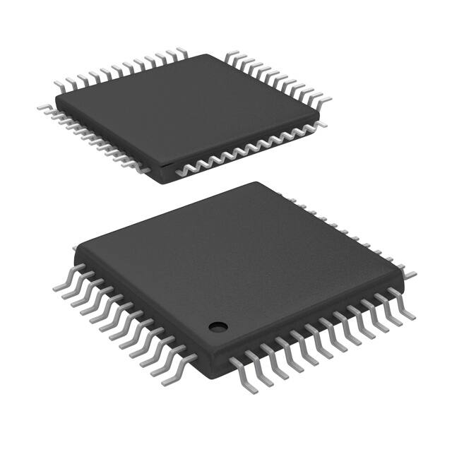
The ADS8381 is available in a 48-lead TQFP package and
is characterized over the industrial −40°C to 85°C
temperature range.
D 48-Pin TQFP Package
BUS 18/16
SAR
+IN
−IN
+
_
Output
Latches
and
3-State
Drivers
CDAC
BYTE
18-/16-/8-Bit
Parallel DATA
Output Bus
Comparator
REFIN
Clock
Conversion
and
Control Logic
CONVST
BUSY
CS
RD
Please be aware that an important notice concerning availability, standard warranty, and use in critical applications of Texas Instruments
semiconductor products and disclaimers thereto appears at the end of this data sheet.
������
�� ��
� ��!"#$%&�"� �' ()##*�& %' "! +),-�(%&�"� .%&*/ �#".)(&'
("�!"#$ &" '+*(�!�(%&�"�' +*# &0* &*#$' "!
*1%' �'&#)$*�&' '&%�.%#. 2%##%�&3/
�#".)(&�"� +#"(*''��4 ."*' �"& �*(*''%#�-3 ��(-).* &*'&��4 "! %-- +%#%$*&*#'/
Copyright 2002−2005, Texas Instruments Incorporated
��������
www.ti.com
SLAS364D − APRIL 2002 − REVISED FEBRUARY 2005
These devices have limited built-in ESD protection. The leads should be shorted together or the device placed in conductive foam during
storage or handling to prevent electrostatic damage to the MOS gates.
ORDERING INFORMATION
MODEL
MAXIMUM
INTEGRAL
LINEARITY
(LSB)
ADS8381I
ADS8381IB
MAXIMUM
DIFFERENTIAL
LINEARITY
(LSB)
±6
±5
−2/3
−1/2
NO
MISSING
CODES
RESOLUTION (BIT)
PACKAGE
TYPE
17
48 Pin
TQFP
18
48 Pin
TQFP
PACKAGE
DESIGNATOR
TEMPERATURE
RANGE
PFB
−40 C to
−40°C
85°C
PFB
−40 C to
−40°C
85°C
ORDERING
INFORMATION
TRANSPORT
MEDIA
QUANTITY
ADS8381IPFBT
Tape and
reel 250
ADS8381IPFBR
Tape and
reel 1000
ADS8381IBPFBT
Tape and
reel 250
ADS8381IBPFBR
Tape and
reel 1000
NOTE: For the most current package and ordering information, see the Package Option Addendum at the end of this document, or see the TI website
at www.ti.com.
ABSOLUTE MAXIMUM RATINGS
over operating free-air temperature range unless otherwise noted(1)
UNIT
Voltage
Voltage range
+IN to AGND
−0.4 V to +VA + 0.1 V
−IN to AGND
−0.4 V to 0.5 V
+VA to AGND
−0.3 V to 7 V
+VBD to BDGND
+VA to +VBD
−0.3 V to 7 V
−0.3 V to 2.55 V
Digital input voltage to BDGND
−0.3 V to +VBD + 0.3 V
Digital output voltage to BDGND
−0.3 V to +VBD + 0.3 V
Operating free-air temperature range, TA
−40°C to 85°C
Storage temperature range, Tstg
−65°C to 150°C
Junction temperature (TJ max)
Power dissipation
TQFP package
θJA thermal impedance
Vapor phase (60 sec)
Lead temperature, soldering
Infrared (15 sec)
150°C
(TJMax − TA)/θJA
86°C/W
215°C
220°C
(1) Stresses beyond those listed under “absolute maximum ratings” may cause permanent damage to the device. These are stress ratings only, and
functional operation of the device at these or any other conditions beyond those indicated under “recommended operating conditions” is not
implied. Exposure to absolute-maximum-rated conditions for extended periods may affect device reliability.
2
��������
www.ti.com
SLAS364D − APRIL 2002 − REVISED FEBRUARY 2005
SPECIFICATIONS
TA = −40°C to 85°C, +VA = 5 V, +VBD = 3 V or 5 V, Vref = 4.096 V, fSAMPLE = 580 kHz (unless otherwise noted)
ADS8381IB
ADS8381I
TEST
PARAMETER
CONDITIONS
MIN
TYP
MAX
MIN
TYP
MAX
UNIT
Analog Input
Full-scale input voltage (see Note 1)
Absolute input voltage
+IN − −IN
0
+IN
−0.2
Vref
Vref + 0.2
−IN
−0.2
0.2
Input capacitance
Input leakage current
0
−0.2
Vref
Vref + 0.2
−0.2
0.2
V
V
45
45
pF
1
1
nA
18
Bits
System Performance
Resolution
18
No missing codes
Integral linearity (see Notes 2 and 3)
18
Bits
< 0.125 FS
−4
−2.2/1
4
−5
5
> 0.125 FS
−5
−3/2
5
−6
6
−1
−0.6/1.25
2
−2
3
−0.75
±0.25
Differential linearity
Offset error
Gain error (see Note 4)
−0.075
Noise
Power supply rejection ratio
17
At 3FFFFh
output code
0.75
−1
0.075
−0.1
±0.5
1
0.1
LSB
(18 bit)
LSB
(18 bit)
mV
%FS
60
60
µV RMS
75
75
dB
Sampling Dynamics
Conversion time
Acquisition time
1.4
0.3
µs
580
kHz
µs
0.3
Throughput rate
Aperture delay
1.4
580
4
4
ns
Aperture jitter
15
15
ps
Step response
150
150
ns
150
150
ns
Over voltage recovery
(1) Ideal input span, does not include gain or offset error.
(2) LSB means least significant bit
(3) This is endpoint INL, not best fit.
(4) Measured relative to an ideal full-scale input (+IN − −IN) of 4.096 V
3
��������
www.ti.com
SLAS364D − APRIL 2002 − REVISED FEBRUARY 2005
SPECIFICATIONS (CONTINUED)
TA = −40°C to 85°C, +VA = +5 V, +VBD = 3 V or 5 V, Vref = 4.096 V, fSAMPLE = 580 kHz (unless otherwise noted)
ADS8381IB
ADS8381I
TEST
PARAMETER
CONDITIONS
MIN
TYP
MAX
MIN
TYP
UNIT
MAX
UNIT
Dynamic Characteristics
Total harmonic distortion (THD) (see Note 1)
Signal to noise ratio (SNR) (see Note 1)
Signal to noise + distortion
(SINAD) (see Note 1)
Spurious free dynamic range (SFDR) (see
Note 1)
1 kHz
−112
−110
10 kHz
−106
−100
50 kHz
−98
−95
100 kHz
−95
−90
1 kHz
88
87
10 kHz
88
87
50 kHz
88
87
100 kHz
88
87
1 kHz
88
87
10 kHz
88
87
50 kHz
87
86
100 kHz
87
86
1 kHz
113
112
10 kHz
108
98
50 kHz
99
96
100 kHz
97
90
3
3
−3dB Small signal bandwidth
dB
dB
dB
dB
MHz
Voltage Reference Input
Reference voltage at REFIN, Vref
Reference resistance (see Note 2)
Reference current drain
fs = 580 kHz
(1) Calculated on the first nine harmonics of the input frequency
(2) Can vary ±20%
4
2.5
4.096
4.2
500
2.5
4.096
4.2
500
1
V
kΩ
1
mA
��������
www.ti.com
SLAS364D − APRIL 2002 − REVISED FEBRUARY 2005
SPECIFICATIONS (CONTINUED)
TA = −40°C to 85°C, +VA = +5 V, +VBD = 3 V or 5 V, Vref = 4.096 V, fSAMPLE = 580 kHz (unless otherwise noted)
PARAMETER
TEST CONDITIONS
MIN
TYP
MAX
UNIT
Digital Input/Output
Logic family
Logic level
CMOS
VIH
VIL
IIH = 5 µA
IIL = 5 µA
VOH
VOL
IOH = 2 TTL loads
IOL = 2 TTL loads
+VBD−1
+VBD + 0.3
0.8
−0.3
V
+VBD − 0.6
0.4
Straight
Binary
Data format
Power Supply Requirements
Power supply voltage
+VBD Buffer supply
2.7
+VA Analog supply
4.75
Supply current, 580-kHz sample rate (see Note 1)
Power dissipation, 580-kHz sample rate (see Note 1)
3.3
5.25
V
5
5.25
23
26
mA
V
115
130
mW
85
°C
Temperature Range
Operating free-air
−40
(1) This includes only +VA current. +VBD current is typical 1 mA with 5 pF load capacitance on all output pins.
5
��������
www.ti.com
SLAS364D − APRIL 2002 − REVISED FEBRUARY 2005
TIMING CHARACTERISTICS
All specifications typical at −40°C to 85°C, +VA = +VBD = 5 V (see Notes 1, 2, and 3)
PARAMETER
MIN
TYP
MAX
µs
tCONV
tACQ
Conversion time
tHOLD
tpd1
Sampling capacitor hold time
25
ns
CONVST low to conversion started (BUSY high)
45
ns
tpd2
tpd3
Propagation delay time, End of conversion to BUSY low
20
ns
Propagation delay time, from start of conversion (internal state) to rising edge of BUSY
20
ns
tw1
tsu1
Pulse duration, CONVST low
40
600
ns
Setup time, CS low to CONVST low
20
tw2
Pulse duration, CONVST high
20
Acquisition time
1.4
UNIT
CONVST falling edge jitter
tw3
tw4
th1
Pulse duration, BUSY signal low
ns
ns
10
40
ps
µs
Min(tACQ)
Pulse duration, BUSY signal high
Hold time, First data bus data transition (CS low for read cycle, or RD or BYTE or
BUS18/16 input changes) after CONVST low
µs
0.3
1.4
µs
600
ns
td1
tsu2
Delay time, CS low to RD low
tw5
ten
Pulse duration, RD low time
td2
td3
Delay time, data hold from RD high
Delay time, BUS18/16 or BYTE rising edge or falling edge to data valid
10
tw6
tw7
Pulse duration, RD high
20
ns
Pulse duration, CS high time
Setup time, RD high to CS high
0
ns
0
ns
50
Enable time, RD low (or CS low for read cycle) to data valid
ns
20
5
ns
ns
20
ns
20
ns
th2
Hold time, last CS rising edge or changes of RD, BYTE, or BUS18/16 to CONVST
falling edge
125
ns
tpd4
Propagation delay time, BUSY falling edge to next RD (or CS for read cycle) falling
edge
Max(td5)
ns
0
ns
td4
tsu3
Delay time, BYTE edge to BUS18/16 edge skew
Setup time, BYTE or BUS18/16 transition to RD falling edge
10
ns
th3
Hold time, BYTE or BUS18/16 transition to RD falling edge
10
ns
tdis
Disable time, RD High (CS high for read cycle) to 3-stated data bus
20
ns
td5
Delay time, BUSY low to MSB data valid
30
ns
tsu5
Setup time, BYTE transition to next BYTE transition, or BUS18/16 transition to next
BUS18/16 transition
50
tsu(AB)
Setup time, from the falling edge of CONVST (used to start the valid conversion) to the
next falling edge of CONVST (when CS = 0 and CONVST used to abort) or to the next
falling edge of CS (when CS is used to abort).
65
1000
ns
tf(CONVST)
Falling time, (CONVST falling edge)
10
30
ns
ns
tsu6
Setup time, CS falling edge to CONVST falling edge when RD = 0
125
ns
(1) All input signals are specified with tr = tf = 5 ns (10% to 90% of +VBD) and timed from a voltage level of (VIL + VIH)/2 except for CONVST.
(2) See timing diagrams.
(3) All timing are measured with 20 pF equivalent loads on all data bits and BUSY pins.
6
��������
www.ti.com
SLAS364D − APRIL 2002 − REVISED FEBRUARY 2005
TIMING CHARACTERISTICS
All specifications typical at −40°C to 85°C, +VA = 5 V, +VBD = 3 V (see Notes 1, 2, and 3)
PARAMETER
MIN
TYP
MAX
µs
tCONV
tACQ
Conversion time
tHOLD
tpd1
Sampling capacitor hold time
25
ns
CONVST low to conversion started (BUSY high)
50
ns
tpd2
tpd3
Propagation delay time, end of conversion to BUSY low
25
ns
Propagation delay time, from start of conversion (internal state) to rising edge of BUSY
25
ns
tw1
tsu1
Pulse duration, CONVST low
40
600
ns
Setup time, CS low to CONVST low
20
tw2
Pulse duration, CONVST high
20
Acquisition time
1.4
UNIT
µs
0.3
CONVST falling edge jitter
ns
ns
10
ps
µs
tw3
tw4
Pulse duration, BUSY signal low
Min(tACQ)
th1
Hold time, first data bus transition (CS low for read cycle, or RD or BYTE or BUS 18/16
input changes) after CONVST low
td1
tsu2
Delay time, CS low to RD low
tw5
ten
Pulse duration, RD low
td2
td3
Delay time, data hold from RD high
10
Delay time, BUS18/16 or BYTE rising edge or falling edge to data valid
10
tw6
tw7
Pulse duration, RD high time
20
ns
20
ns
th2
Hold time, last CS rising edge or changes of RD, BYTE, or BUS18/16 to CONVST
falling edge
125
ns
tpd4
Propagation delay time, BUSY falling edge to next RD (or CS for read cycle) falling
edge
Max(td5)
ns
td4
tsu3
Delay time, BYTE edge to BUS18/16 edge skew
0
ns
Setup time, BYTE or BUS18/16 transition to RD falling edge
10
ns
th3
Hold time, BYTE or BUS18/16 transition to RD falling edge
10
ns
tdis
Disable time, RD High (CS high for read cycle) to 3-stated data bus
30
ns
td5
Delay time, BUSY low to MSB data valid delay time
40
ns
tsu5
Setup time, BYTE transition to next BYTE transition, or BUS18/16 transition to next
BUS18/16 transition
50
tsu(AB)
Setup time, from the falling edge of CONVST (used to start the valid conversion) to the
next falling edge of CONVST (when CS = 0 and CONVST used to abort) or to the next
falling edge of CS (when CS is used to abort).
70
1000
ns
tf(CONVST)
Falling time, (CONVST falling edge)
10
30
ns
Pulse duration, BUSY signal high
Setup time, RD high to CS high
40
µs
ns
0
ns
0
ns
50
Enable time, RD low (or CS low for read cycle) to data valid
Pulse duration, CS high time
1.4
600
ns
30
ns
ns
30
ns
ns
tsu6
Setup time, CS falling edge to CONVST falling edge when RD = 0
125
ns
(1) All input signals are specified with tr = tf = 5 ns (10% to 90% of +VBD) and timed from a voltage level of (VIL + VIH)/2 except for CONVST.
(2) See timing diagrams.
(3) All timing are measured with 10 pF equivalent loads on all data bits and BUSY pins.
7
��������
www.ti.com
SLAS364D − APRIL 2002 − REVISED FEBRUARY 2005
PIN ASSIGNMENTS
BUSY
DB0
DB1
DB2
DB3
DB4
DB5
DB6
DB7
DB8
DB9
BDGND
PFB PACKAGE
(TOP VIEW)
36 35 34 33 32 31 30 29 28 27 26 25
37
24
38
23
39
22
40
21
41
20
42
19
43
18
44
17
45
16
46
15
47
14
48
3
4 5
6 7 8
13
9 10 11 12
REFIN
NC
NC
+VA
AGND
+IN
−IN
AGND
+VA
+VA
1 2
NC − No connection.
8
AGND
AGND
+VBD
BUS18/16
BYTE
CONVST
RD
CS
+VA
AGND
AGND
+VA
REFM
REFM
+VBD
DB10
DB11
DB12
DB13
DB14
DB15
DB16
DB17
AGND
AGND
+VA
��������
www.ti.com
SLAS364D − APRIL 2002 − REVISED FEBRUARY 2005
TERMINAL FUNCTIONS
NAME
AGND
NO.
I/O
5, 8, 11,
12, 14, 15,
44, 45
−
Analog ground
DESCRIPTION
BDGND
25
−
Digital ground for buffer supply
BUSY
36
O
Status output. High when a conversion is in progress.
BUS18/16
38
I
Bus size select input. Used for selecting 18-bit or 16-bit wide bus transfer.
0: Data bits output on the 18-bit data bus pins DB[17:0].
1: Last two data bits D[1:0] from 18-bit wide bus output on:
a) the low byte pins DB[9:2] if BYTE = 0
b) the high byte pins DB[17:10] if BYTE = 1
BYTE
39
I
Byte select input. Used for 8-bit bus reading.
0: No fold back
1: Low byte D[9:2] of the 16 most significant bits is folded back to high byte of the 16 most significant pins
DB[17:10].
CONVST
40
I
Convert start. The falling edge of this input ends the acquisition period and starts the hold period.
CS
42
I
Chip select. The falling edge of this input starts the acquisition period.
8-Bit Bus
BYTE = 0
Data Bus
16-Bit Bus
BYTE = 1
BUS18/16 = 0
BUS18/16 = 0
BYTE = 1
BUS18/16 = 1
BYTE = 0
BUS18/16 = 0
18-Bit Bus
BYTE = 0
BUS18/16 = 1
BYTE = 0
BUS18/16 = 0
DB17
16
O
D17 (MSB)
D9
All ones
D17 (MSB)
All ones
D17 (MSB)
DB16
17
O
D16
D8
All ones
D16
All ones
D16
DB15
18
O
D15
D7
All ones
D15
All ones
D15
DB14
19
O
D14
D6
All ones
D14
All ones
D14
DB13
20
O
D13
D5
All ones
D13
All ones
D13
DB12
21
O
D12
D4
All ones
D12
All ones
D12
DB11
22
O
D11
D3
D1
D11
All ones
D11
DB10
23
O
D10
D2
D0(LSB)
D10
All ones
D10
DB9
26
O
D9
All ones
All ones
D9
All ones
D9
DB8
27
O
D8
All ones
All ones
D8
All ones
D8
DB7
28
O
D7
All ones
All ones
D7
All ones
D7
DB6
29
O
D6
All ones
All ones
D6
All ones
D6
DB5
30
O
D5
All ones
All ones
D5
All ones
D5
DB4
31
O
D4
All ones
All ones
D4
All ones
D4
DB3
32
O
D3
All ones
All ones
D3
D1
D3
DB2
33
O
D2
All ones
All ones
D2
D0 (LSB)
D2
DB1
34
O
D1
All ones
All ones
D1
All ones
D1
DB0
35
O
D0 (LSB)
All ones
All ones
D0 (LSB)
All ones
D0 (LSB)
−IN
7
I
Inverting input channel
+IN
6
I
Noninverting input channel
NC
2, 3
−
No connection
REFIN
1
I
Reference input.
REFM
47, 48
I
Reference ground.
RD
41
I
Synchronization pulse for the parallel output. When CS is low, this serves as the output enable and puts the
previous conversion result on the bus.
+VA
4, 9, 10,
13, 43, 46
−
Analog power supplies, 5-V dc
24, 37
−
Digital power supply for buffer
+VBD
9
��������
www.ti.com
SLAS364D − APRIL 2002 − REVISED FEBRUARY 2005
TIMING DIAGRAMS
tw2
tw1
CONVST
tpd1
tpd2
tw4
tw3
BUSY
tsu1
tw7
CS
tpd3
CONVERT†
tHOLD
tCONV
tCONV
SAMPLING†
(When CS Toggle)
tACQ
BYTE
tsu(AB)
tsu(AB)
tsu5
BUS 18/16
th1
tsu5
tsu5
tsu5
tsu2
tpd4
th2
td1
RD
tdis
ten
DB[17:12]
Hi−Z
MSB
Hi−Z
D[17:12] D[9:4]
DB[11:10]
Hi−Z
Hi−Z
D[11:10] D[3:2] D[1:0]
DB[9:0]
Hi−Z
Hi−Z
D[9:0]
†Signal internal to device
Figure 1. Timing for Conversion and Acquisition Cycles With CS and RD Toggling
10
��������
www.ti.com
SLAS364D − APRIL 2002 − REVISED FEBRUARY 2005
tw1
tw2
CONVST
tpd1
tw4
tpd2
tw3
BUSY
tw7
tsu6
tsu6
CS
tpd3
CONVERT†
tCONV
tCONV
tHOLD
SAMPLING†
(When CS Toggle)
tACQ
tsu(AB)
tsu(AB)
tsu5
BYTE
tsu5
th1
tsu5
tsu5
BUS 18/16
tsu2
tpd4
ten
DB[17:12]
th2
ten
RD = 0
ten
tdis
Previous
Hi−Z
D [17:12]
tdis
Hi−Z
MSB
Hi−Z
Previous
D [17:12]
Hi−Z
Previous
D [11:10]
Hi−Z
Previous
D [9:0]
D[17:12] D[9:4]
DB[11:10]
Hi−Z
Previous
D [11:10]
Hi−Z
D[11:10] D[3:2] D[1:0]
DB[9:0]
Hi−Z
Previous
D [9:0]
Hi−Z
D[9:0]
†Signal internal to device
Figure 2. Timing for Conversion and Acquisition Cycles With CS Toggling, RD Tied to BDGND
11
��������
www.ti.com
SLAS364D − APRIL 2002 − REVISED FEBRUARY 2005
tw1
tw2
CONVST
tpd1
tpd2
tw4
tw3
BUSY
CS = 0
tpd3
CONVERT†
tCONV
tCONV
tHOLD
t(ACQ)
SAMPLING†
(When CS = 0)
tsu(AB)
tsu(AB)
tsu5
BYTE
tsu5
th1
tpd4
th2
tsu5
BUS18/16
tsu5
RD
tdis
ten
DB[17:12]
Hi−Z
MSB
Hi−Z
D[17:12] D[9:4]
DB[11:10]
Hi−Z
Hi−Z
D[11:10] D[3:2] D[1:0]
DB[9:0]
Hi−Z
Hi−Z
D[9:0]
†Signal internal to device
Figure 3. Timing for Conversion and Acquisition Cycles With CS Tied to BDGND, RD Toggling
12
��������
www.ti.com
SLAS364D − APRIL 2002 − REVISED FEBRUARY 2005
tw2
tw1
CONVST
tpd1
tw4
tpd2
tw3
BUSY
CS = 0
CONVERT†
tCONV
tCONV
tpd3
tpd3
tHOLD
tHOLD
t(ACQ)
SAMPLING†
(When CS = 0)
tsu(AB)
tsu(AB)
BYTE
tsu5
tsu5
th1
th1
tdis
BUS 18/16
tsu5
tsu5
RD = 0
td5
DB[17:12]
Next D[17:12]
D[17:12] D[9:4]
DB[11:10]
Previous D[1:0]
D[1:0]
D[11:10] D[3:2]
Next D[11:10]
DB[9:0]
D[9:0]
Next D[9:0]
†Signal internal to device
Figure 4. Timing for Conversion and Acquisition Cycles With CS and RD Tied to BDGND—Auto Read
13
��������
www.ti.com
SLAS364D − APRIL 2002 − REVISED FEBRUARY 2005
CS
RD
BYTE
BUS 18/16
ten
ten
DB[17:0]
Hi−Z
tdis
Valid
Hi−Z
td3
tdis
td3
Valid
Valid
Figure 5. Detailed Timing for Read Cycles
14
Hi−Z
��������
www.ti.com
SLAS364D − APRIL 2002 − REVISED FEBRUARY 2005
TYPICAL CHARACTERISTICS(1)
HISTOGRAM (DC CODE SPREAD)
HALF SCALE 65536 CONVERSIONS
9000
+VA = 5 V,
+VBD = 3 V,
TA = 255C,
fs = 580 kHz,
Vref = 4.096 V,
Input = 0.5 FSR
8000
7000
Count
6000
5000
4000
3000
2000
1000
131030
131031
131032
131033
131034
131035
131036
131037
131038
131039
131040
131041
131042
131043
131044
131045
131046
131047
131048
131049
131050
131051
131052
131053
131054
131055
131056
131057
131058
0
code
Figure 6
GAIN ERROR
vs
FREE-AIR TEMPERATURE
GAIN ERROR
vs
FREE-AIR TEMPERATURE
0.08
E G − Gain Error − %FS
0.06
0.1
+VA = 5 V,
+VBD = 5 V,
fs = 580 kHz,
Vref = 4.096 V
0.08
0.06
E G − Gain Error − %FS
0.1
0.04
0.02
0
−0.02
0.04
0.02
0
−0.02
−0.04
−0.04
−0.06
−0.06
−0.08
−0.08
−0.1
−40
+VA = 5 V,
+VBD = 5 V,
fS = 580 kHz,
Vref = 2.5 V
−15
10
35
60
TA − Free-Air Temperature − °C
Figure 7
85
−0.1
−40
−15
10
35
60
TA − Free-Air Temperature − °C
85
Figure 8
15
��������
www.ti.com
SLAS364D − APRIL 2002 − REVISED FEBRUARY 2005
OFFSET ERROR
vs
FREE-AIR TEMPERATURE
OFFSET ERROR
vs
FREE-AIR TEMPERATURE
0.5
0.5
0.1
−0.1
0.1
−0.1
−0.3
−0.3
−0.5
−40
+VA = 5 V,
+VBD = 5 V,
fS = 580 kHz,
Vref = 2.5 V
0.3
EO − Offset Error − mV
EO − Offset Error − mV
0.3
+VA = 5 V,
+VBD = 5 V,
fS = 580 kHz,
Vref = 4.096 V
−0.5
−15
10
35
60
TA − Free-Air Temperature − °C
−40
85
−15
10
35
60
TA − Free-Air Temperature − °C
Figure 9
Figure 10
DIFFERENTIAL NONLINEARITY (MAX)
vs
FREE-AIR TEMPERATURE
DNL − Differential Nonlinearity (MAX) −LSBs
DNL − Differential Nonlinearity (MIN) − LSBs
DIFFERENTIAL NONLINEARITY (MIN)
vs
FREE-AIR TEMPERATURE
0
+VA = 5 V,
+VBD = 5 V,
fS = 580 kHz,
Vref = 4 V
−0.2
−0.4
−0.6
−0.8
−1
−40
−15
10
35
60
TA − Free-Air Temperature − °C
Figure 11
16
85
85
2
1.8
1.6
+VA = 5 V,
+VBD = 5 V,
fS = 580 kHz,
Vref = 4 V
1.4
1.2
1
0.8
0.6
0.4
0.2
0
−40
−15
10
35
60
TA − Free-Air Temperature − °C
Figure 12
85
��������
www.ti.com
SLAS364D − APRIL 2002 − REVISED FEBRUARY 2005
INTEGRAL NONLINEARITY (MAX)
vs
FREE-AIR TEMPERATURE
INTEGRAL NONLINEARITY (MIN)
vs
FREE-AIR TEMPERATURE
4
INL − Integral Nonlinearity (MAX) − LSBs
INL − Integral Nonlinearity (MIN) − LSBs
−1
+VA = 5 V,
+VBD = 5 V,
fS = 580 kHz,
Vref = 4 V
−1.5
−2
−2.5
−3
−3.5
−4
−4.5
−15
10
35
60
TA − Free-Air Temperature − °C
3
2.5
2
1.5
1
−40
−5
−40
3.5
85
+VA = 5 V,
+VBD = 5 V,
fS = 580 kHz,
Vref = 4 V
−15
10
35
60
TA − Free-Air Temperature − °C
Figure 13
Figure 14
INTEGRAL NONLINEARITY (MAX)
vs
SAMPLE RATE
INL − Integral Nonlinearity (MIN) − LSBs
−1.5
INL − Integral Nonlinearity (MAX) − LSBs
INTEGRAL NONLINEARITY (MIN)
vs
SAMPLE RATE
−1
+VA = 5 V,
+VBD = 5 V,
TA = 255C,
fS = 580 kHz,
Vref = 4.096 V
−2
−2.5
−3
−3.5
−4
125
250
375
500
Sample Rate − KSPS
Figure 15
85
2.5
2.3
+VA = 5 V,
+VBD = 5 V,
TA = 255C,
fS = 580 kHz,
Vref = 4.096 V
2.1
1.9
1.7
1.5
125
250
375
Sample Rate − KSPS
500
Figure 16
17
��������
www.ti.com
SLAS364D − APRIL 2002 − REVISED FEBRUARY 2005
DIFFERENTIAL NONLINEARITY (MAX)
vs
SAMPLE RATE
−0.5
DNL − Differential Nonlinearity (MAX) − LSBs
DNL − Differential Nonlinearity (MIN) − LSBs
DIFFERENTIAL NONLINEARITY (MIN)
vs
SAMPLE RATE
+VA = 5 V,
+VBD = 5 V,
TA = 255C,
fS = 580 kHz,
Vref = 4.096 V
−0.6
−0.7
−0.8
−0.9
−1
125
250
375
Sample Rate − KSPS
500
1.5
1.3
+VA = 5 V,
+VBD = 5 V,
TA = 255C,
fS = 580 kHz,
Vref = 4.096 V
1.1
0.9
0.7
0.5
125
250
375
Sample Rate − KSPS
Figure 17
Figure 18
OFFSET ERROR
vs
SUPPLY VOLTAGE
GAIN ERROR
vs
SUPPLY VOLTAGE
0
TA = 255C,
fS = 580 kHz,
Vref = 4.096 V
0.01
−0.01
5
VDD − Supply Voltage − V
Figure 19
18
−0.2
−0.3
−0.4
−0.03
−0.05
4.75
TA = 255C,
fS = 580 kHz,
Vref = 4.096 V
−0.1
EO − Offset Error − mV
E G − Gain Error − %FS
0.05
0.03
500
5.25
−0.5
4.75
5
VDD − Supply Voltage − V
Figure 20
5.25
��������
www.ti.com
SLAS364D − APRIL 2002 − REVISED FEBRUARY 2005
DIFFERENTIAL NONLINEARITY (MIN)
vs
SUPPLY VOLTAGE
DNL − Differential Nonlinearity (MIN) − LSBs
+VA ANALOG SUPPLY CURRENT
vs
SUPPLY VOLTAGE
23
+VA − Supply Current − mA
22.5
TA = 255C,
fS = 580 kHz,
Vref = 4.096 V
22
21.5
21
20.5
20
4.75
5
+VA − Supply Voltage − V
5.25
−0.5
TA = 255C,
fS = 580 kHz,
Vref = 4.096 V
−0.6
−0.7
−0.8
−0.9
−1
4.75
5
VDD − Supply Voltage − V
Figure 21
Figure 22
INTEGRAL NONLINEARITY (MIN)
vs
SUPPLY VOLTAGE
−2
INL − Integral Nonlinearity (MIN) − LSBs
DNL − Differential Nonlinearity (MAX) − LSBs
DIFFERENTIAL NONLINEARITY (MAX)
vs
SUPPLY VOLTAGE
1.5
TA = 255C,
fS = 580 kHz,
Vref = 4.096 V
1.3
1.1
0.9
0.7
0.5
4.75
5.25
5
VDD − Supply Voltage − V
Figure 23
5.25
−2.2
TA = 255C,
fS = 580 kHz,
Vref = 4.096 V
−2.4
−2.6
−2.8
−3
4.75
5
VDD − Supply Voltage − V
5.25
Figure 24
19
��������
www.ti.com
SLAS364D − APRIL 2002 − REVISED FEBRUARY 2005
DIFFERENTIAL NONLINEARITY (MIN)
vs
REFERENCE VOLTAGE
DNL − Differential Nonlinearity (MIN) − LSBs
INTEGRAL NONLINEARITY (MAX)
vs
SUPPLY VOLTAGE
INL − Integral Nonlinearity (MAX) − LSBs
2.5
TA = 255C,
fS = 580 kHz,
Vref = 4.096 V
2.3
2.1
1.9
1.7
1.5
4.75
5
5.25
−0.5
−0.6
+VBD = 5 V,
+VA = 5 V,
TA = 255C,
fS = 580 kHz
−0.7
−0.8
−0.9
−1
2.5
2.7
2.9
Figure 25
3.9
4.1
−1
INL − Integral Nonlinearity (MIN) − LSBs
DNL − Differential Nonlinearity (MAX) − LSBs
3.7
Figure 26
+VBD = 5 V,
+VA = 5 V,
TA = 255C,
fS = 580 kHz
1.6
1.4
1.2
+VBD = 5 V,
+VA = 5 V,
TA = 255C,
fS = 580 kHz
−1.5
−2
−2.5
−3
−3.5
−4
1
2.5
2.7
2.9
3.1
3.3
3.5
3.7
Vref − Reference Voltage − V
Figure 27
20
3.5
INTEGRAL NONLINEARITY (MIN)
vs
REFERENCE VOLTAGE
DIFFERENTIAL NONLINEARITY (MAX)
vs
REFERENCE VOLTAGE
1.8
3.3
Vref − Reference Voltage − V
VDD − Supply Voltage − V
2
3.1
3.9
4.1
2.5
2.7
2.9 3.1 3.3 3.5
3.7 3.9
Vref − Reference Voltage − V
Figure 28
4.1
��������
www.ti.com
SLAS364D − APRIL 2002 − REVISED FEBRUARY 2005
OFFSET ERROR
vs
REFERENCE VOLTAGE
INTEGRAL NONLINEARITY (MAX)
vs
REFERENCE VOLTAGE
−0.1
3.5
+VBD = 5 V,
+VA = 5 V,
TA = 255C,
fS = 580 kHz
+VBD = 5 V,
+VA = 5 V,
TA = 255C,
fS = 580 kHz
−0.12
−0.14
EO − Offset Error − mV
INL − Integral Nonlinearity (MAX) − LSBs
4
3
2.5
2
−0.16
−0.18
−0.20
−0.22
−0.24
−0.26
1.5
−0.28
1
2.5
−0.3
2.7
2.9
3.1
3.3
3.5
3.7
3.9
2.5
4.1
Vref − Reference Voltage − V
2.7
2.9 3.1 3.3 3.5 3.7 3.9
Vref − Reference Voltage − V
Figure 29
Figure 30
TOTAL HARMONIC DISTORTION
vs
FREE-AIR TEMPERATURE
SIGNAL-TO-NOISE RATIO
vs
FREE-AIR TEMPERATURE
−85
90
89
88.5
+VBD = 3 V,
+VA = 5 V,
TA = 255C,
fi = 100 kHz,
fS = 580 kHz,
Vref = 4 V
−87
THD − Total Harmonic Distortion − dB
SNR − Signal-to-Noise Ratio − dB
89.5
88
87.5
87
86.5
86
−89
−91
−93
+VBD = 3 V,
+VA = 5 V,
TA = 255C,
fi = 100 kHz,
fS = 580 kHz,
Vref = 4 V,
Input = FSR
−95
−97
−99
−101
−103
85.5
85
−40
4.1
−15
10
35
60
TA − Free-Air Temperature − °C
Figure 31
85
−105
−40
−15
10
35
60
85
TA − Free-Air Temperature − °C
Figure 32
21
��������
www.ti.com
SLAS364D − APRIL 2002 − REVISED FEBRUARY 2005
SIGNAL-TO-NOISE AND DISTORTION
vs
FREE-AIR TEMPERATURE
SPURIOUS FREE DYNAMIC RANGE
vs
FREE-AIR TEMPERATURE
90
120
110
+VBD = 3 V,
+VA = 5 V,
TA = 255C,
fi = 100 kHz,
fS = 580 kHz,
Vref = 4 V,
Input = FSR
SINAD − Signal-to-Nois and Distortion − dB
SFDR − Spurious Free Dynamic Range − dB
130
100
90
80
70
−15
10
35
60
TA − Free-Air Temperature − °C
89
88
87
86
85
−40
60
−40
+VBD = 3 V,
+VA = 5 V,
TA = 255C,
fi = 100 kHz,
fS = 580 kHz,
Vref = 4 V,
Input = FSR
85
−15
Figure 33
89
+VBD = 3 V,
+VA = 5 V,
TA = 255C,
fi = 100 kHz,
fS = 580 kHz,
Vref = 4.096 V,
Input = FSR
14.2
14
13.8
13.6
13.4
88.4
88.2
88
87.8
87.6
87.4
87
−15
10
35
60
TA − Free-Air Temperature − °C
Figure 35
22
88.6
87.2
13.2
13
−40
85
+VBD = 3 V,
+VA = 5 V,
TA = 255C,
fS = 580 kHz,
Vref = 4.096 V,
Input = FSR
88.8
SNR − Signal-to-Noise Ratio − dB
ENOB − Effective Number of Bits − Bits
14.4
60
SIGNAL-TO-NOISE RATIO
vs
INPUT FREQUENCY
15
14.6
35
Figure 34
EFFECTIVE NUMBER OF BITS
vs
FREE-AIR TEMPERATURE
14.8
10
TA − Free-Air Temperature − °C
85
1
10
fi − Input Frequency − kHz
Figure 36
100
��������
www.ti.com
SLAS364D − APRIL 2002 − REVISED FEBRUARY 2005
SIGNAL-TO-NOISE AND DISTORTION
vs
INPUT FREQUENCY
TOTAL HARMONIC DISTORTION
vs
INPUT FREQUENCY
90
THD − Total Harmonic Distortion − dB
−80
−90
SINAD − Signal-to-Nois and Distortion − dB
+VBD = 3 V,
+VA = 5 V,
TA = 255C,
fS = 580 kHz,
Vref = 4.096 V,
Input = FSR
−100
−110
−120
+VBD = 3 V,
+VA = 5 V,
TA = 255C,
fS = 580 kHz,
Vref = 4.096 V,
Input = FSR
89
88
87
86
85
−130
1
10
fi − Input Frequency − kHz
1
100
10
fi − Input Frequency − kHz
Figure 37
Figure 38
SPURIOUS FREE DYNAMIC RANGE
vs
INPUT FREQUENCY
EFFECTIVE NUMBER OF BITS
vs
INPUT FREQUENCY
140
+VBD = 3 V,
+VA = 5 V,
TA = 255C,
fS = 580 kHz,
Vref = 4.096 V,
Input = FSR
SFDR − Spurious Free Dynamic Range − dB
ENOB − Effective Number of Bits − Bits
15
14.8
100
14.6
14.4
14.2
+VBD = 3 V,
+VA = 5 V,
TA = 255C,
fS = 580 kHz,
Vref = 4.096 V,
Input = FSR
130
120
110
100
90
80
70
60
14
1
10
fi − Input Frequency − kHz
Figure 39
100
1
10
fi − Input Frequency − kHz
100
Figure 40
23
��������
www.ti.com
SLAS364D − APRIL 2002 − REVISED FEBRUARY 2005
SUPPLY CURRENT
vs
FREE-AIR TEMPERATURE
ANALOG (+VA) SUPPLY CURRENT
vs
SAMPLE RATE
23
22.7
+VBD = 5.25 V,
+VA = 5.25 V,
fS = 580 kHz,
Vref = 4.096 V,
22.5
+VA − Supply Current − mA
V DD − Supply Current − mA
22.6
+VBD = 5.25 V,
+VA = 5.25 V,
TA = 255C,
Vref = 4.096 V,
22.5
22.4
22.3
22
21.5
21
20.5
22.2
20
22.1
−40
19.5
−15
10
35
60
TA − Free-Air Temperature − °C
125
85
Figure 41
250
375
Samply Rate − KSPS
500
Figure 42
INL − LSBs
INTEGRAL NONLINEARITY
5
4
3
2
1
0
−1
−2
−3
−4
−5
+VBD = 5 V,
+VA = 5 V,
TA = 255C,
fS = 580 kHz
0
65536
131072
Code
Figure 43
24
196608
262144
��������
www.ti.com
SLAS364D − APRIL 2002 − REVISED FEBRUARY 2005
DNL − LSBs
DIFFERENTIAL NONLINEARITY
5
4
3
2
1
0
−1
−2
−3
−4
−5
+VBD = 5 V,
+VA = 5 V,
TA = 255C,
fS = 580 kHz
0
65536
131072
Code
196608
262144
Figure 44
FFT
0
+VBD = 3 V, +VA = 5 V, TA = 255C,
fi = 100 kHz, Vref = 4.096 V,
fS = 580 kHz, 4096 points
−20
Amplitude − dB
−40
−60
−80
−100
−120
−140
−160
−180
0
45000
90000
135000
180000
225000
270000
fi − Input Frequency − Hz
Figure 45
25
��������
www.ti.com
SLAS364D − APRIL 2002 − REVISED FEBRUARY 2005
APPLICATION INFORMATION
MICROCONTROLLER INTERFACING
ADS8381 to 8-Bit Microcontroller Interface
Figure 46 shows a parallel interface between the ADS8381 and a typical microcontroller using the 8-bit data bus.
The BUSY signal is used as a falling-edge interrupt to the microcontroller.
Analog 5 V
REF 3040
0.1 µF
OUT
AGND
10 µF
Ext Ref Input 100 Ω
0.1 µF
Micro
Controller
GPIO
GPIO
GPIO
GPIO
RD
AD[7:0]
−IN
+IN
+VA
REFIN
REFM
AGND
Analog Input
Digital 3 V
1000 Ω
CS
AD8381
BYTE
BUS18/16
CONVST
RD
DB[17:10]
0.1 µF
BDGND
BDGND
+VBD
Figure 46. ADS8381 Application Circuitry
26
��������
www.ti.com
SLAS364D − APRIL 2002 − REVISED FEBRUARY 2005
PRINCIPLES OF OPERATION
The ADS8381 is a high-speed successive approximation register (SAR) analog-to-digital converter (ADC). The
architecture is based on charge redistribution which inherently includes a sample/hold function. See Figure 46 for
the application circuit for the ADS8381.
The conversion clock is generated internally. The conversion time of 1.4 µs is capable of sustaining a 580-kHz
throughput.
The analog input is provided to two input pins: +IN and −IN. When a conversion is initiated, the differential input on
these pins is sampled on the internal capacitor array. While a conversion is in progress, both inputs are disconnected
from any internal function.
REFERENCE
The ADS8381 can operate with an external reference with a range from 2.5 V to 4.2 V. The reference voltage on the
input pin 1 (REFIN) of the converter is internally buffered. A clean, low noise, well-decoupled reference voltage on
this pin is required to ensure good performance of the converter. A low noise band-gap reference like the REF3040
can be used to drive this pin. A 0.1-uF decoupling capacitor is required between pin 1 and pin 48 of the converter.
This capacitor should be placed as close as possible to the pins of the device. Designers should strive to minimize
the routing length of the traces that connect the terminals of the capacitor to the pins of the converter. An RC network
can also be used to filter the reference voltage. A 100-Ω series resistor and a 0.1-uF capacitor, which can also serve
as the decoupling capacitor, can be used to filter the reference voltage.
ANALOG INPUT
When the converter enters the hold mode, the voltage difference between the +IN and −IN inputs is captured on the
internal capacitor array. The voltage on the −IN input is limited between –0.2 V and 0.2 V, allowing the input to reject
small signals which are common to both the +IN and −IN inputs. The +IN input has a range of –0.2 V to Vref + 0.2 V.
The input span (+IN − (−IN)) is limited to 0 V to Vref.
The input current on the analog inputs depends upon a number of factors: sample rate, input voltage, and source
impedance. Essentially, the current into the ADS8381 charges the internal capacitor array during the sample period.
After this capacitance has been fully charged, there is no further input current. The source of the analog input voltage
must be able to charge the input capacitance (45 pF) to an 18-bit settling level within the acquisition time (300 ns)
of the device. When the converter goes into the hold mode, the input impedance is greater than 1 GΩ.
Care must be taken regarding the absolute analog input voltage. To maintain the linearity of the converter, the +IN
and −IN inputs and the span (+IN − (−IN)) should be within the limits specified. Outside of these ranges, the
converter’s linearity may not meet specifications. To minimize noise, low bandwidth input signals with low-pass filters
should be used.
Care should be taken to ensure that the output impedance of the sources driving the +IN and −IN inputs are matched.
If this is not observed, the two inputs could have different setting times. This may result in offset error, gain error, and
linearity error which changes with temperature and input voltage.
The analog input to the converter needs to be driven with a low noise, high-speed op-amp like the THS4031. An RC
filter is recommended at the input pins to low-pass filter the noise from the source. A series resistor of 15 Ω and a
decoupling capacitor of 1.2 nF is recommended.
The input to the converter is a unipolar input voltage in the range 0 V to Vref. The THS4031 can be used in the source
follower configuration to drive the converter.
27
��������
www.ti.com
SLAS364D − APRIL 2002 − REVISED FEBRUARY 2005
ADS8381
+ _
Unipolar Input
THS4031
_ +
15 Ω
+IN
1.2 nF
−IN
50 Ω
Figure 47. Unipolar Input to Converter
In systems where the input is bipolar, the THS4031 can be used in the inverting configuration with an additional DC
bias applied to its + input so as to keep the input to the ADS8381 within its rated operating voltage range. This
configuration is also recommended when the ADS8381 is used in signal processing applications where good SNR
and THD performance is required. The DC bias can be derived from the REF3020 or the REF3040 reference voltage
ICs. The input configuration shown below is capable of delivering better than 88-dB SNR and –95-db THD at an input
frequency of 100 kHz. In case bandpass filters are used to filter the input, care should be taken to ensure that the
signal swing at the input of the bandpass filter is small so as to keep the distortion introduced by the filter minimal.
In such cases, the gain of the circuit shown in Figure 48 can be increased to keep the input to the ADS8381 large
to keep the SNR of the system high. Note that the gain of the system from the + input to the output of the THS4031
in such a configuration is a function of the gain of the AC signal. A resistor divider can be used to scale the output
of the REF3020 or REF3040 to reduce the voltage at the DC input to THS4031 to keep the voltage at the input of
the converter within its rated operating range.
ADS8381
+ _
Vdc
Vac
360 Ω
THS4031
100 Ω
_ +
+IN
33 nF
−IN
360 Ω
Figure 48. Bipolar Input to Converter
DIGITAL INTERFACE
Timing And Control
See the timing diagrams in the specifications section for detailed information on timing signals and their requirements.
The ADS8381 uses an internal oscillator generated clock which controls the conversion rate and in turn the
throughput of the converter. No external clock input is required.
Conversions are initiated by bringing the CONVST pin low for a minimum of 40 ns (after the 40 ns minimum
requirement has been met, the CONVST pin can be brought high), while CS is low. The BUSY output is brought high
immediately following CONVST going low. BUSY stays high throughout the conversion process and returns low when
the conversion has ended. Sampling starts with the falling edge of the BUSY signal when CS is tied low or starts with
the falling edge of CS when BUSY is low.
Both RD and CS can be high during and before a conversion with one exception (CS must be low when CONVST
goes low to initiate a conversion). Both the RD and CS pins are brought low in order to enable the parallel output bus
with the conversion.
28
��������
www.ti.com
SLAS364D − APRIL 2002 − REVISED FEBRUARY 2005
Digital Inputs
The converter switches from sample to hold mode at the falling edge of the CONVST input pin. A clean and low jitter
falling edge is important to the performance of the converter. A sharp falling transition on this pin can affect the voltage
that is acquired by the converter. A falling transition time in the range of 10 ns to 30 ns is required to achieve the rated
performance of the converter. A resistor of approximately 1000 Ω (10% tolerance) can be placed in series with the
CONVST input pin to satisfy this requirement.
The other digital inputs to the ADS8381 do not require any resistors in series with them. However, certain precautions
are necessary to ensure that transitions on these inputs do not affect converter performance. It is recommended that
all activity on the input pins happen during the first 600 ns of the conversion period. This allows the error correction
circuits inside the device to correct for any errors that these activities cause on the converter output. For example,
when the converter is operated with CS and RD tied to ground, the signal CONVST can be brought low to initiate
a conversion and brought high after a duration not exceeding 600 ns. Figure 49 shows the recommended timing for
the CONVST input with RD and CS tied low.
tacq
tconv
125 ns(1)
600 ns
800 ns(1)
tw1 125 ns
RD
BUSY
(1)Quiet Zone (No bus activity)
Figure 50. Bus Activity Split to Avoid Quiet Zone
If the RD pin is brought high to three-state the data buses, the three-stating operation should occur 125 ns before
the end of the acquisition phase. Figure 51 shows the recommended timing for using the ADS8381 in this mode of
operation. The same principle applies to other bus activities such as BYTE and BUS18/16.
tacq
tconv
125 ns(1)
800 ns(1)
600 ns
tw1 < 600 ns
CONVST
CS = 0
RD
th2 > 125 ns
BUSY
(1)Quiet Zone (No bus activity)
Figure 51. Read Timing if the Bus Needs to be Three-Stated
30
��������
www.ti.com
SLAS364D − APRIL 2002 − REVISED FEBRUARY 2005
Reading Data
The ADS8381 outputs full parallel data in straight binary format as shown in Table 1. The parallel output is active when
CS and RD are both low. Any other combination of CS and RD sets the parallel output to 3-state. BYTE and BUS18/16
are used for multiword read operations. BYTE is used whenever lower bits on the bus are output on the higher byte
of the bus. BUS18/16 is used whenever the last two bits on the 18-bit bus is output on either bytes of the higher 16-bit
bus. Refer to Table 1 for ideal output codes.
Table 1. Ideal Input Voltages and Output Codes
DESCRIPTION
ANALOG VALUE
Full scale range
(+Vref)
(+Vref)/262144
Least significant bit (LSB)
+Full scale
Midscale
Midscale – 1 LSB
Zero
DIGITAL OUTPUT
STRAIGHT BINARY
BINARY CODE
HEX CODE
(+Vref) – 1 LSB
(+Vref)/2
11 1111 1111 1111 1111
3FFFF
10 0000 0000 0000 0000
20000
(+Vref)/2 – 1 LSB
0V
01 1111 1111 1111 1111
1FFFF
00 0000 0000 0000 0000
00000
The output data is a full 18-bit word (D17−D0) on DB17–DB0 pins (MSB−LSB) if both BUS18/16 and BYTE are low.
The result may also be read on an 16-bit bus by using only pins DB17−DB2. In this case two reads are necessary:
the first as before, leaving both BUS18/16 and BYTE low and reading the 16 most significant bits (D17−D2) on pins
DB17−DB2, then bringing BUS18/16 high while holding BYTE low. When BUS18/16 is high, the lower two bits
(D1–D0) appear on pins DB3−DB2.
The result may also be read on an 8-bit bus for convenience. This is done by using only pins DB17−DB10. In this
case three reads are necessary: the first as before, leaving both BUS18/16 and BYTE low and reading the 8 most
significant bits on pins DB17−DB10, then bringing BYTE high while holding BUS18/16 low. When BYTE is high, the
medium bits (D9−D2) appear on pins DB17−DB10. The last read is done by bringing BUS18/16 high while holding
BYTE high. When BUS18/16 is high, the lower two bits (D1–D0) appear on pins DB11−DB10. The last read cycle
is not necessary if only the first 16 most significant bits are of interest.
All of these multiword read operations can be performed with multiple active RD (toggling) or with RD held low for
simplicity. This is referred to as the AUTO READ operation.
Table 2. Conversion Data Read Out
DATA READ OUT
BYTE
BUS18/16
DB17−DB12 PINS
DB11−DB10 PINS
DB9−DB4 PINS
DB3−DB2 PINS
DB1−DB0 PINS
High
High
All One’s
D1−D0
All One’s
All One’s
All One’s
Low
High
All One’s
All One’s
All One’s
D1−D0
All One’s
High
Low
D9−D4
D3−D2
All One’s
All One’s
All One’s
Low
Low
D17−D12
D11−D10
D9−D4
D3−D2
D1−D0
RESET
The device can be reset through the use of the combination fo CS and CONVST. Since the BUSY signal is held at
high during the conversion, either one of these conditions triggers an internal self-clear reset to the converter.
D Issue a CONVST when CS is low and internal CONVERT state is high. The falling edge of CONVST starts a
reset.
D Issue a CS (select the device) while internal CONVERT state is high. The falling edge of CS causes a reset.
Once the device is reset, all output latches are cleared (set to zeroes) and the BUSY signal is brought low. A new
sampling period is started at the falling edge of the BUSY signal immediately after the instant of the internal reset.
31
��������
www.ti.com
SLAS364D − APRIL 2002 − REVISED FEBRUARY 2005
INITIALIZATION
At first power on there are three read cycles required (RD must be toggled three times). If conversion cycle is
attempted before these initialization read cycles, the first three conversion cycles will not produce valid results. This
is used to load factory trimming data for a specific device to assure high accuracy of the converter. Because of this
requirement, the RD pin cannot be tied permanently to BDGND. System designers can still achieve the AUTO READ
function if the power-on requirement is satisfied.
LAYOUT
For optimum performance, care should be taken with the physical layout of the ADS8381 circuitry.
As the ADS8381 offers single-supply operation, it will often be used in close proximity with digital logic,
microcontrollers, microprocessors, and digital signal processors. The more digital logic present in the design and the
higher the switching speed, the more difficult it is to achieve good performance from the converter.
The basic SAR architecture is sensitive to glitches or sudden changes on the power supply, reference, ground
connections and digital inputs that occur just prior to latching the output of the analog comparator. Thus, driving any
single conversion for an n-bit SAR converter, there are at least n windows in which large external transient voltages
can affect the conversion result. Such glitches might originate from switching power supplies, nearby digital logic,
or high power devices.
The degree of error in the digital output depends on the reference voltage, layout, and the exact timing of the external
event.
On average, the ADS8381 draws very little current from an external reference as the reference voltage is internally
buffered. If the reference voltage is external and originates from an op amp, make sure that it can drive the bypass
capacitor or capacitors without oscillation. A 0.1-µF bypass capacitor is recommended from pin 1 (REFIN) directly
to pin 48 (REFM). REFM and AGND should be shorted on the same ground plane under the device.
The AGND and BDGND pins should be connected to a clean ground point. In all cases, this should be the analog
ground. Avoid connections which are too close to the grounding point of a microcontroller or digital signal processor.
If required, run a ground trace directly from the converter to the power supply entry point. The ideal layout consists
of an analog ground plane dedicated to the converter and associated analog circuitry.
As with the AGND connections, +VA should be connected to a 5-V power supply plane or trace that is separate from
the connection for digital logic until they are connected at the power entry point. Power to the ADS8381 should be
clean and well bypassed. A 0.1-µF ceramic bypass capacitor should be placed as close to the device as possible.
See Table 3 for the placement of the capacitor. In addition, a 1-µF to 10-µF capacitor is recommended. In some
situations, additional bypassing may be required, such as a 100-µF electrolytic capacitor or even a Pi filter made up
of inductors and capacitors—all designed to essentially low-pass filter the 5-V supply, removing the high frequency
noise.
Table 3. Power Supply Decoupling Capacitor Placement
POWER SUPPLY PLANE
SUPPLY PINS
CONVERTER ANALOG SIDE
CONVERTER DIGITAL SIDE
Pin pairs that require shortest path to decoupling capacitors
(4,5), (8,9), (10,11), (13,15),
(43,44), (45,46)
(24,25)
Pins that require no decoupling
12, 14
37
32
�PACKAGE OPTION ADDENDUM
www.ti.com
7-Oct-2021
PACKAGING INFORMATION
Orderable Device
Status
(1)
Package Type Package Pins Package
Drawing
Qty
Eco Plan
(2)
Lead finish/
Ball material
MSL Peak Temp
Op Temp (°C)
Device Marking
(3)
(4/5)
(6)
ADS8381IBPFBT
ACTIVE
TQFP
PFB
48
250
RoHS & Green
Call TI
Level-2-260C-1 YEAR
-40 to 85
ADS8381I
B
(1)
The marketing status values are defined as follows:
ACTIVE: Product device recommended for new designs.
LIFEBUY: TI has announced that the device will be discontinued, and a lifetime-buy period is in effect.
NRND: Not recommended for new designs. Device is in production to support existing customers, but TI does not recommend using this part in a new design.
PREVIEW: Device has been announced but is not in production. Samples may or may not be available.
OBSOLETE: TI has discontinued the production of the device.
(2)
RoHS: TI defines "RoHS" to mean semiconductor products that are compliant with the current EU RoHS requirements for all 10 RoHS substances, including the requirement that RoHS substance
do not exceed 0.1% by weight in homogeneous materials. Where designed to be soldered at high temperatures, "RoHS" products are suitable for use in specified lead-free processes. TI may
reference these types of products as "Pb-Free".
RoHS Exempt: TI defines "RoHS Exempt" to mean products that contain lead but are compliant with EU RoHS pursuant to a specific EU RoHS exemption.
Green: TI defines "Green" to mean the content of Chlorine (Cl) and Bromine (Br) based flame retardants meet JS709B low halogen requirements of


 工商网监
湘ICP备2023018690号
工商网监
湘ICP备2023018690号
