�������
�� ��
�����
�
� � ��� ������� ���
ADS8382
SLAS416B – JUNE 2004 – REVISED NOVEMBER 2004
18-BIT, 600-kHz, FULLY DIFFERENTIAL PSEUDO-BIPOLAR INPUT,
MICROPOWER SAMPLING ANALOG-TO-DIGITAL CONVERTER
WITH SERIAL INTERFACE AND REFERENCE
FEATURES
APPLICATIONS
•
•
•
•
•
•
•
•
•
•
•
•
•
•
•
•
•
•
600-kHz Sample Rate
±1.25 LSB Typ, ±3 LSB Max INL
18-Bit NMC Ensured Over Temperature
SINAD 96 dB, SFDR 120 dB at fi = 1 kHz
High-Speed Serial Interface up to 40 MHz
Onboard Reference Buffer
Onboard 4.096-V Reference
Pseudo-Bipolar Input, up to ±4.2 V
Onboard Conversion Clock
Zero Latency
Wide Digital Supply
Low Power
– 115 mW at 600 kHz
– 15 mW During Nap Mode
– 10 µW During Power Down
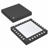
28-Pin 6 × 6 QFN Package
Medical Instruments
Optical Networking
Transducer Interface
High Accuracy Data Acquisition Systems
Magnetometers
DESCRIPTION
The ADS8382 is a high performance 18-bit, 600-kHz
A/D converter with fully differential, pseudo-bipolar
input. The device includes an 18-bit capacitor-based
SAR A/D converter with inherent sample and hold.
The ADS8382 offers a high-speed CMOS serial
interface with clock speeds up to 40 MHz.
The ADS8382 is available in a 28 lead 6 × 6 QFN
package and is characterized over the industrial
–40°C to 85°C temperature range.
High Speed SAR Converter Family
Type/Speed
18-Bit Pseudo-Diff
500 kHz
~ 600 kHz
ADS8383
750 kHZ
1 MHz
1.25 MHz
2 MHz
3 MHz
4 MHz
ADS8381
ADS8380 (S)
18-Bit Pseudo-Bipolar, Fully Diff
ADS8382 (S)
16-Bit Pseudo-Diff
ADS8401/05
ADS8411
16-Bit Pseudo-Bipolar, Fully Diff
ADS8371
ADS8402/06
ADS8412
14-Bit Pseudo-Diff
ADS7890 (S)
12-Bit Pseudo-Diff
ADS7891
ADS7886
SAR
+IN
−IN
+
_
CDAC
ADS7881
Output
Latches
and
3-State
Drivers
FS
SCLK
SDO
Comparator
REFIN
REFOUT
4.096-V
Internal
Reference
Clock
Conversion
and
Control Logic
CS
CONVST
BUSY
PD
Please be aware that an important notice concerning availability, standard warranty, and use in critical applications of Texas
Instruments semiconductor products and disclaimers thereto appears at the end of this data sheet.
PRODUCTION DATA information is current as of publication date.
Products conform to specifications per the terms of the Texas
Instruments standard warranty. Production processing does not
necessarily include testing of all parameters.
Copyright © 2004, Texas Instruments Incorporated
�ADS8382
www.ti.com
SLAS416B – JUNE 2004 – REVISED NOVEMBER 2004
These devices have limited built-in ESD protection. The leads should be shorted together or the device
placed in conductive foam during storage or handling to prevent electrostatic damage to the MOS gates.
ORDERING INFORMATION (1)
MODEL
MAXIMUM
INTEGRAL
LINEARITY
(LSB)
MAXIMUM
DIFFERENTIAL
LINEARITY
(LSB)
NO
MISSING
CODES
RESOLUTION
(BIT)
PACKAGE
TYPE
PACKAGE
DESIGNATOR
TEMPERATURE
RANGE
ADS8382I
±5
-2/2.5
17
28 Pin
6×6 QFN
RHP
-40°C to 85°C
28 Pin
6×6 QFN
RHP
ADS8382IB
(1)
±3
-1/1.5
18
ORDERING
INFORMATION
TRANSPORT
MEDIA
QUANTITY
ADS8382IRHPT
Small Tape and
Reel 250
ADS8382IRHPR
Tape and Reel
2500
ADS8382IBRHPT
Small Tape and
Reel 250
ADS8382IBRHPR
Tape and
Reel 2500
-40°C to 85°C
For the most current specifications and package information, refer to our web site at www.ti.com
ABSOLUTE MAXIMUM RATINGS
over operating free-air temperature range (unless otherwise noted) (1)
UNIT
Voltage
+IN to AGND
–0.3 V to +VA + 0.3 V
–IN to AGND
–0.3 V to +VA + 0.3 V
+VA to AGND
–0.3 V to 7 V
+VBD to BDGND
Digital input voltage to BDGND
–0.3 V to 7 V
–0.3 V to +VBD + 0.3 V
Digital input voltage to +VA
+0.3 V
Operating free-air temperature range, TA
–40°C to 85°C
Storage temperature range, Tstg
–65°C to 150°C
Junction temperature (TJ max)
QFN package
Lead temperature, soldering
(1)
2
150°C
Power dissipation
(TJ max – TA)/θJA
θJA thermal impedance
86°C/W
Vapor phase (60 sec)
215°C
Infrared (15 sec)
220°C
Stresses beyond those listed under "absolute maximum ratings" may cause permanent damage to the device. These are stress ratings
only, and functional operation of the device at these or any other conditions beyond those indicated under "recommended operating
conditions" is not implied. Exposure to absolute-maximum-rated conditions for extended periods may affect device reliability.
�ADS8382
www.ti.com
SLAS416B – JUNE 2004 – REVISED NOVEMBER 2004
SPECIFICATIONS
At –40°C to 85°C, +VA = +5 V, +VBD = +5 V or +VBD = +2.7 V, using internal or external reference, fSAMPLE = 600 kHz,
unless otherwise noted. (All performance parameters are valid only after device has properly resumed from power down,
Table 2.)
PARAMETER
TEST CONDITIONS
ADS8382IB
MIN
TYP
ADS8382I
MAX
MIN
TYP
MAX
UNIT
ANALOG INPUT
Full-scale
input voltage (1)
Absolute input voltage
+IN – (–IN)
–Vref
Vref
–Vref
Vref
+IN
–0.2
Vref + 0.2
-0.2
Vref + 0.2
–IN
–0.2
Vref + 0.2
-0.2
Vref + 0.2
(Vref/2) –0.2
(Vref/2) +0.2
(Vref/2) –0.2
(Vref/2) +0.2
Input common mode
range
Sampling capacitance
(measured between +IN
to AGND and -IN to
AGND)
Input leakage current
V
V
V
40
40
pF
1
1
nA
18
Bits
SYSTEM PERFORMANCE
Resolution
18
No missing codes
Integral linearity (2) (3) (4)
INL
DNL
Differential linearity (3)
EO
Offset error
Quiet zones observed
±1.25
–1
±0.6
Quiet zones not observed
Quiet zones observed
Quiet zones not observed
–0.75
Common-mode rejection
ratio
–5
5
LSB
(18 bit)
1.5
–2
2.5
LSB
(18 bit)
0.75
–1.5
1.5
mV
0.075
-0.1
0.1
%FS
±1.25
–0.075
CMRR
Bits
3
±2
(3)
Gain
17
–3
error (3) (5)
EG
PSRR
18
±0.25
At DC
80
80
[+IN + (–IN)]/2 = 50 mVp-p
at 1 MHz + DC of Vref/2
55
55
Noise
At 00000H output code
40
40
µV RMS
DC Power supply rejection ratio
At 10000H output code
55
55
dB
dB
SAMPLING DYNAMICS
Conversion time
1.16
Acquisition time
0.50
1000
Throughput rate
600
Aperture delay
10
Aperture jitter
Step response
1.16
0.50
µs
1000
µs
600
kHz
10
ns
12
12
ps RMS
400
400
ns
400
400
ns
VIN = 8 Vp-p at 1 kHz
-116
-116
VIN = 8 Vp-p at 10 kHz
-115
-115
VIN = 8 Vp-p at 100 kHz
-96
-96
VIN = 8 Vp-p at 1 kHz
96
96
VIN = 8 Vp-p at 10 kHz
95
95
VIN = 8 Vp-p at 100 kHz
94
94
(6)
Overvoltage recovery
DYNAMIC CHARACTERISTICS
THD
SNR
(1)
(2)
(3)
(4)
(5)
(6)
(7)
Total harmonic
distortion (3) (7)
Signal-to-noise ratio (3)
dB
dB
Ideal input span; does not include gain or offset error.
LSB means least significant bit.
Measured using analog input circuit in Figure 54 and digital stimulus in Figure 58 and Figure 59 and reference voltage of 4.096 V.
This is endpoint INL, not best fit.
Measured using external reference source so does not include internal reference voltage error or drift.
Defined as sampling time necessary to settle an initial error of 2Vref on the sampling capacitor to a final error of 1 LSB at 18-bit level.
Measured using the input circuit in Figure 54.
Calculated on the first nine harmonics of the input frequency.
3
�ADS8382
www.ti.com
SLAS416B – JUNE 2004 – REVISED NOVEMBER 2004
SPECIFICATIONS (continued)
At –40°C to 85°C, +VA = +5 V, +VBD = +5 V or +VBD = +2.7 V, using internal or external reference, fSAMPLE = 600 kHz,
unless otherwise noted. (All performance parameters are valid only after device has properly resumed from power down,
Table 2.)
PARAMETER
SINAD
SFDR
TEST CONDITIONS
Signal-to-noise
+ distortion (3) (7)
Spurious free dynamic
range (3)
ADS8382IB
MIN
TYP
ADS8382I
MAX
MIN
TYP
VIN = 8 Vp-p at 1 kHz
96
96
VIN = 8 Vp-p at 10 kHz
95
95
VIN = 8 Vp-p at 100 kHz
92
92
VIN = 8 Vp-p at 1 kHz
120
120
VIN = 8 Vp-p at 10 kHz
120
120
VIN = 8 Vp-p at 100 kHz
99
99
75
75
–3dB Small signal
bandwidth
MAX
UNIT
dB
dB
MHz
REFERENCE INPUT
Reference voltage input
range
Vref
2.5
Resistance (8)
4.096
4.2
2.5
10
4.096
4.2
10
V
MΩ
INTERNAL REFERENCE OUTPUT
Vref
Reference voltage range
IOUT = 0 A, TA = 30°C
Source current
Static load
4.088
4.096
4.104
4.088
4.096
Line regulation
+VA = 4.75 V to 5.25 V
2.5
2.5
mV
Drift
IOUT = 0 A
25
25
ppm/°C
10
4.104
V
10
µA
DIGITAL INPUT/OUTPUT
Logic family CMOS
VIH
High level input voltage
+VBD – 1
+VBD + 0.3
+VBD – 1
+VBD + 0.3
V
VIL
Low level input voltage
–0.3
0.8
–0.3
0.8
V
VOH
High level output voltage
IOH = 2 TTL loads
VOL
Low level output voltage
IOL = 2 TTL loads
+VBD –0.6
+VBD –0.6
V
0.4
0.4
V
Data format 2's complement (MSB first)
POWER SUPPLY REQUIREMENTS
Power supply
voltage
+VA
+VBD
Supply current, 600-kHz
sample rate (9)
ICC
4.75
5
5.25
4.75
5
5.25
V
2.7
3.3
5.25
2.7
3.3
5.25
V
22
25
22
25
+VA = 5 V
mA
POWER DOWN
ICC(PD)
Supply current, power
down
2
2
µA
3
3
mA
NAP MODE
ICC(NAP)
Supply current, nap
mode
Power-up time from nap
300
300
ns
85
°C
TEMPERATURE RANGE
Specified performance
(8)
(9)
4
–40
85
–40
Can vary +/-30%.
This includes only +VA current. With +VBD = 5 V, +VBD current is typically 1 mA with a 10-pF load capacitance on the digital output
pins.
�ADS8382
www.ti.com
SLAS416B – JUNE 2004 – REVISED NOVEMBER 2004
TIMING REQUIREMENTS
(1) (2) (3) (4) (5) (6)
PARAMETER
Conversion time
tconv
ADS8382I/ADS8382IB
MIN
TYP
MAX
UNIT
REF
FIGURE
1000
1160
ns
43,44,
45,46
tacq1
Acquisition time in normal mode
0.5
1000
µs
43,44,46
tacq2
Acquisition time in nap mode (tacq2 = tacq1 + td18)
0.8
1000
µs
45
CONVERSION AND SAMPLING
tquiet1
Quite sampling time (last toggle of interface signals to convert start
command) (6)
30
ns
42,43,44,
45,47,48,
49
tquiet2
Quite sampling time (convert start command to first toggle of interface
signals) (6)
10
ns
42,43,44,
45,47,48,
49
600
ns
42,43,44,
45,47,49
tquiet3
Quite conversion time (last toggle of interface signals to fall of BUSY) (6)
tsu1
Setup time, CONVST before BUSY fall
15
ns
43
tsu2
Setup time, CS before BUSY fall (only for conversion/sampling control)
20
ns
42,43
tsu4
Setup time, CONVST before CS rise (so CONVST can be recognized)
5
ns
43,44,46
th1
Hold time, CS after BUSY fall (only for conversion/sampling control)
0
ns
43
th3
Hold time, CONVST after CS rise
7
ns
45
th4
Hold time, CONVST after CS fall (to ensure width of CONVST_QUAL) (4)
20
ns
44
tw1
CONVST pulse duration
20
ns
45
tw2
CS pulse duration
10
ns
43,44
tw5
Pulse duration, time between conversion start command and conversion
abort command to successfully abort the ongoing conversion
ns
46
ns
47,48,49
1000
DATA READ OPERATION
tcyc
SCLK period
SCLK duty cycle
25
40%
60%
tsu5
Setup time, CS fall before first SCLK fall
10
ns
47
tsu6
Setup time, CS fall before FS rise
7
ns
48,49
tsu7
Setup time, FS fall before first SCLK fall
7
ns
48,49
th5
Hold time, CS fall after SCLK fall
3
ns
47
th6
Hold time, FS fall after SCLK fall
7
ns
48,49
tsu2
Setup time, CS fall before BUSY fall (only for read control)
20
ns
42,47
tsu3
Setup time, FS fall before BUSY fall (only for read control)
20
ns
42,49
th2
Hold time, CS fall after BUSY fall (only for read control)
15
ns
42,47
th8
Hold time, FS fall after BUSY fall (only for read control)
15
ns
42,49
tw2
CS pulse duration
10
ns
47
tw3
FS pulse duration
10
ns
48,49
PD pulse duration for reset and power down
60
ns
55,56
All unspecified pulse durations
10
ns
MISCELLANEOUS
tw4
(1)
(2)
(3)
(4)
(5)
(6)
All input signals are specified with tr = tf = 5 ns (10% to 90% of VDD) and timed from a voltage level of (VIL + VIH)/2.
All specifications typical at –40°C to 85°C, +VA = +4.75 V to +5.25 V, +VBD = +2.7 V to +5.25 V.
All digital output signals loaded with 10-pF capacitors.
CONVST_QUAL is CONVST latched by a low value on CS (see Figure 41).
Reference figure indicated is only a representative of where the timing is applicable and is not exhaustive.
Quiet time zones are for meeting performance and not functionality.
5
�ADS8382
www.ti.com
SLAS416B – JUNE 2004 – REVISED NOVEMBER 2004
TIMING CHARACTERISTICS (1) (2) (3) (4)
PARAMETER
ADS8382I/ADS8382IB
MIN
TYP
UNIT
REF
FIGURE
10
ns
43,45
MAX
CONVERSION AND SAMPLING
td1
Delay time, conversion start command to conversion start (aperture delay)
td2
Delay time, conversion end to BUSY fall
td4
Delay time, conversion start command to BUSY rise
td3
Delay time, CONVST rise to sample start
td5
td6
5
ns
43,44,45
20
ns
43
5
ns
45
Delay time, CS fall to sample start
10
ns
45
Delay time, conversion abort command to BUSY fall
10
ns
46
DATA READ OPERATION
td12 Delay time, CS fall to MSB valid
3
15
ns
47
td15 Delay time, FS rise to MSB valid
6
18
ns
48,49
18
ns
49
10
ns
47,48,49
6
ns
47
55
ns
55,56
300
ns
57
td7
Delay time, BUSY fall to MSB valid (if FS is high when BUSY falls)
td13 Delay time, SCLK rise to bit valid
2
td14 Delay time, CS rise to SDO 3-state
MISCELLANEOUS
td10 Delay time, PD rise to SDO 3-state
Nap mode
td18
Delay time, total
device resume
time
Full power down (external reference used with or without
1-µF||0.1-µF capacitor on REFOUT)
td11 + 2x
conversions
Full power down (internal reference used with or without
1-µF||0.1-µF capacitor on REFOUT)
25 (4)
ms
55
1
td11 Delay time, untrimmed circuit full power-down resume time
td16
Delay time, device
power-down time
td17
Delay time, trimmed internal reference settling (either by turning on supply or
resuming from full power-down mode), with 1-µF||0.1-µF capacitor on REFOUT
(1)
(2)
(3)
(4)
6
Nap
Full power down (internal/external reference used)
56
ms
55,56
200
ns
57
10
µs
55,56
ms
55
4
All input signals are specified with tr = tf = 5 ns (10% to 90% of VDD) and timed from a voltage level of (VIL + VIH)/2.
All specifications typical at –40°C to 85°C, +VA = +4.75 V to +5.25 V, +VBD = +2.7 V to +5.25 V.
All digital output signals loaded with 10-pF capacitors.
Including td11, two conversions (time to cycle CONVST twice), and td17.
�ADS8382
www.ti.com
SLAS416B – JUNE 2004 – REVISED NOVEMBER 2004
PIN ASSIGNMENTS
28
27
26
25
24
23
22
PD
FS
CS
CONVST
SCLK
SDO
BUSY
TOP VIEW
1
AGND
BDGND
21
2
AGND
+VBD
20
3
+VA
AGND
19
4
AGND
AGND
18
5
AGND
+VA
17
6
+VA
+VA
16
7
REFM
AGND
15
+VA
−IN
12
14
+IN
11
NC
NC
10
13
REFOUT
9
8
REFIN
ADS8382
TERMINAL FUNCTIONS
PIN
I/O
DESCRIPTION
NAME
NO.
AGND
1, 2, 4, 5,
15, 18, 19
–
Analog ground pins. AGND must be shorted to analog ground plane below the device.
BDGND
21
–
Digital ground for all digital inputs and outputs. BDGND must be shorted to the analog ground plane below
the device.
BUSY
22
O
Status output. This pin is high when conversion is in progress.
CONVST
25
I
Convert start. This signal is qualified with CS internally.
CS
26
I
Chip select
FS
27
I
Frame sync. This signal is qualified with CS internally.
+IN
11
I
Noninverting analog input channel
–IN
12
I
Inverting analog input channel
NC
10, 13
–
No connection
PD
28
I
Power down. Device resets and powers down when this signal is high.
REFIN
8
I
Reference (positive) input. REFIN must be decoupled with REFM pin using 0.1-µF bypass capacitor and
1-µF storage capacitor.
REFM
7
I
Reference ground. To be connected to analog ground plane.
REFOUT
9
O
Internal reference output. Shorted to REFIN pin only when internal reference is used.
SCLK
24
I
Serial clock. Data is shifted onto SDO with the rising edge of this clock. This signal is qualified with CS
internally.
SDO
23
O
Serial data out. All bits except MSB are shifted out at the rising edge of SCLK.
+VA
3, 6, 14,
16, 17
–
Analog power supplies
20
–
Digital power supply for all digital inputs and outputs.
+VBD
7
�ADS8382
www.ti.com
SLAS416B – JUNE 2004 – REVISED NOVEMBER 2004
TYPICAL CHARACTERISTICS
SIGNAL-TO-NOISE RATIO
vs
REFERENCE VOLTAGE
SIGNAL-TO-NOISE
AND DISTORTION
vs
REFERENCE VOLTAGE
96
95
94
93
92
SFDR − Spurious Free Dynamic Range − dB
91
2.5
3
3.5
Vref − Reference Voltage − V
4
97
SINAD − Signal−to−Noise and Distortion − dB
fi = 1 kHz,
+VA = 5 V,
+VBD = 5 V,
TA = 25°C
95
94
93
92
91
2.5
4
Figure 2.
SPURIOUS FREE DYNAMIC RANGE
vs
REFERENCE VOLTAGE
TOTAL HARMONIC DISTORTION
vs
REFERENCE VOLTAGE
121.5
−116.2
fi = 1 kHz,
+VA = 5 V,
+VBD = 5 V,
TA = 25°C
121
120.5
fi = 1 kHz,
+VA = 5 V,
+VBD = 5 V,
TA = 25°C
−116.4
−116.6
−116.8
120
119.5
−117
−117.2
119
−117.4
118.5
−117.6
118
117.5
−117.8
3
3.5
4
2.5
Vref − Reference Voltage − V
3
3.5
4
Vref − Reference Voltage − V
Figure 3.
Figure 4.
EFFECTIVE NUMBER OF BITS
vs
REFERENCE VOLTAGE
EFFECTIVE NUMBER OF BITS
vs
FREE-AIR TEMPERATURE
16
ENOB − Effective Number of Bits − Bits
15.7
ENOB − Effective Number of Bits − Bits
3
3.5
Vref − Reference Voltage − V
Figure 1.
2.5
fi = 1 kHz,
+VA = 5 V,
+VBD = 5 V,
TA = 25°C
15.6
15.5
15.4
15.3
15.2
15.1
15
14.9
15.9
15.8
+VA = 5 V,
+VBD = 5 V,
REFIN = 4.096 V,
fi = 1 kHz
15.7
15.6
15.5
15.4
15.3
15.2
15.1
15
14.8
2.5
3
3.5
Vref − Reference Voltage − V
Figure 5.
8
fi = 1 kHz,
+VA = 5 V,
+VBD = 5 V,
TA = 25°C
96
THD − Total Harmonic Distortion − dB
SNR − Signal-to-Noise Ratio − dB
97
4
−40 −25 −10 5
20 35 50 65
TA − Free-Air Temperature − °C
Figure 6.
80
�ADS8382
www.ti.com
SLAS416B – JUNE 2004 – REVISED NOVEMBER 2004
TYPICAL CHARACTERISTICS (continued)
SIGNAL-TO-NOISE
AND DISTORTION
vs
FREE-AIR TEMPERATURE
SNR − Signal-to-Noise Ratio − dB
97
fi = 1 kHz
+VA = 5 V,
+VBD = 5 V,
REFIN = 4.096 V
96.8
96.6
96.4
96.2
96
95.8
95.6
95.4
95.2
−40 −25 −10 5
20
35
50
65
80
fi = 1 kHz
+VA = 5 V,
+VBD = 5 V,
REFIN = 4.096 V
96.6
96.4
96.2
96
95.8
95.6
95.4
95.2
95
−40 −25 −10 5
20
35
50
65
80
TA − Free-Air Temperature − °C
Figure 7.
Figure 8.
SPURIOUS FREE DYNAMIC RANGE
vs
FREE-AIR TEMPERATURE
TOTAL HARMONIC DISTORTION
vs
FREE-AIR TEMPERATURE
125
123
121
119
117
fi = 1 kHz,
+VA = 5 V,
+VBD = 5 V,
REFIN = 4.096 V
115
5
20
35
50
65
80
−118
−120
fi = 1 kHz,
+VA = 5 V,
+VBD = 5 V,
REFIN = 4.096 V
5
20
35
50
65
TA − Free-Air Temperature − °C
Figure 9.
Figure 10.
EFFECTIVE NUMBER OF BITS
vs
INPUT FREQUENCY
SIGNAL-TO-NOISE
AND DISTORTION
vs
INPUT FREQUENCY
SINAD − Signal-To-Noise and Distortion − dB
15.5
15
+VA = 5 V,
+VBD = 5 V,
REFIN = 4.096 V
TA = 25°C
14
1
−116
TA − Free-Air Temperature − °C
16
14.5
−114
−122
−40 −25 −10
113
−40 −25 −10
ENOB − Effective Number of Bits − Bits
97
96.8
TA − Free-Air Temperature − °C
THD − Total Harmonic Distortion − dB
SFDR − Spurious Free Dynamic Range − dB
95
SINAD − Signal-To-Noise and Distortion − dB
SIGNAL-TO-NOISE RATIO
vs
FREE-AIR TEMPERATURE
10
fi − Input Frequency − kHz
Figure 11.
100
97
80
+VA = 5 V,
+VBD = 5 V,
REFIN = 4.096 V
TA = 25°C
96
95
94
93
92
91
90
1
10
fi − Input Frequency − kHz
100
Figure 12.
9
�ADS8382
www.ti.com
SLAS416B – JUNE 2004 – REVISED NOVEMBER 2004
TYPICAL CHARACTERISTICS (continued)
SIGNAL-TO-NOISE RATIO
vs
INPUT FREQUENCY
SPURIOUS FREE DYNAMIC RANGE
vs
INPUT FREQUENCY
SFDR − Spurious Free Dynamic Range − dB
SNR − Signal-to-Noise Ratio − dB
97
+VA = 5 V,
+VBD = 5 V,
REFIN = 4.096 V
TA = 25°C
96
95
94
93
10
fi − Input Frequency − kHz
1
125
120
115
110
105
+VA = 5 V,
+VBD = 5 V,
REFIN = 4.096 V,
TA = 25°C
100
95
1
100
10
100
fi − Input Frequency − kHz
Figure 13.
Figure 14.
TOTAL HARMONIC DISTORTION
vs
INPUT FREQUENCY
THD − Total Harmonic Distortion − dB
−95
+VA = 5 V,
+VBD = 5 V,
REFIN = 4.096 V
TA = 25°C
−100
−105
−110
−115
−120
1
10
fi − Input Frequency − kHz
100
Figure 15.
HISTOGRAM
APPROXIMATELY 20000 CONVERSIONS
WITH A DC INPUT AT MIDSCALE (0 V)
6000
5601
6000
+VA = 5 V,
+VBD = 5 V,
REFIN = 4.096 V
TA = 25°C
5200
5000
5000
3786
3000
+VA = 5 V,
+VBD = 5 V,
REFIN = 4.096 V
TA = 25°C
2460
2000
3000
2582
2000
1383
19
874
472
40
6
1000
301
151
0
−10 −9 −8−7 −6 −5 −4 −3 −2 −1 0 1 2 3 4 5 6 7 8 9 10 11 12
2’s Complement Code in Decimal
0
1
6
1521
987 211
51
23
2’s Complement Code in Decimal
Figure 16.
10
2
130079
130080
130081
130082
130083
130084
130085
130086
130087
130088
130089
130090
130091
130092
130093
130094
130095
130096
130097
130098
130099
130100
1000
5067 5098
3979
4000
Hits
4000
Hits
HISTOGRAM
APPROXIMATELY 20000 CONVERSIONS
WITH A DC INPUT CLOSE TO FULL SCALE (4 V)
Figure 17.
�ADS8382
www.ti.com
SLAS416B – JUNE 2004 – REVISED NOVEMBER 2004
TYPICAL CHARACTERISTICS (continued)
GAIN ERROR
vs
REFERENCE VOLTAGE
GAIN ERROR
vs
SUPPLY VOLTAGE
0
6
+VA = 5 V,
+VBD = 5 V,
TA = 25°C
−0.1
EG − Gain Error − mV
EG − Gain Error − mV
−0.2
+VBD = 5 V,
REFIN = 4.096 V
TA = 25°C
4
−0.3
−0.4
−0.5
−0.6
−0.7
−0.8
2
0
−2
−4
−0.9
−1
−6
2.5
3
3.5
Vref − Reference Voltage − V
4
4.75
Figure 18.
Figure 19.
GAIN ERROR
vs
FREE-AIR TEMPERATURE
OFFSET ERROR
vs
REFERENCE VOLTAGE
2
5.25
0.75
+VA = 5 V,
+VBD = 5 V,
REFIN = 4.096 V
+VA = 5 V,
+VBD = 5 V,
TA = 25°C
0.5
1
EO − Offset Error − mV
EG − Gain Error − mV
5
+VA − Analog Supply Voltage − V
0
−1
0.25
0
−0.25
−0.5
−2
−40 −25 −10
5
20
35
50
65
−0.75
2.5
80
TA − Free-Air Temperature − °C
Figure 21.
OFFSET ERROR
vs
FREE-AIR TEMPERATURE
OFFSET ERROR
vs
SUPPLY VOLTAGE
4.1
0.5
+VA = 5 V,
+VBD = 5 V,
REFIN = 4.096 V
0.4
0.3
EO − Offset Error − mV
EO − Offset Error − mV
2.9 3.1 3.3 3.5 3.7 3.9
Vref − Reference Voltage − V
Figure 20.
0.75
0.5
2.7
0.25
0
−0.25
+VBD = 5 V,
REFIN = 4.096 V
TA = 25°C
0.2
0.1
0
−0.1
−0.2
−0.3
−0.5
−0.4
−0.75
−40 −25 −10 5
20
35
50
65
TA − Free-Air Temperature − °C
Figure 22.
80
−0.5
4.75
5
5.25
+VA − Analog Supply Voltage − V
Figure 23.
11
�ADS8382
www.ti.com
SLAS416B – JUNE 2004 – REVISED NOVEMBER 2004
TYPICAL CHARACTERISTICS (continued)
POWER DISSIPATION
vs
SUPPLY VOLTAGE
POWER DISSIPATION
vs
SAMPLE RATE
140
116
PD − Power Dissipation − mW
114
112
PD − Power Dissipation − mW
+VBD = 5 V,
fs = 600 KSPS
TA = 25°C
110
108
106
104
102
Normal Mode Current
100
80
60
NAP Mode Current
40
+VA = 5 .25 V,
+VBD = 5.25 V,
TA = 25°C
20
0
100
4.75
5
+VA − Analog Supply Voltage − V
0
5.25
300
400
500
600
Figure 25.
POWER DISSIPATION
vs
FREE-AIR TEMPERATURE
DIFFERENTIAL NONLINEARITY
vs
REFERENCE VOLTAGE
4
DNL − Differential Nonlinearity − LSBs
+VA = 5 V,
+VBD = 5 V,
fs = 600 KSPS
115
110
105
+VA = 5 V,
+VBD = 5 V,
TA = 25°C
3
2
Max
1
0
Min
−1
−2
−3
−4
−40 −25 −10 5
20
35
50
65
2.5
80
TA − Free-Air Temperature − °C
2.7
2.9
3.1
3.3
3.5
3.7
3.9
4.1
Vref − Reference Voltage − V
Figure 26.
Figure 27.
INTEGRAL NONLINEARITY
vs
REFERENCE VOLTAGE
DIFFERENTIAL NONLINEARITY
vs
FREE-AIR TEMPERATURE
4
1.5
+VA = 5 V,
+VBD = 5 V,
TA = 25°C
3
DNL − Differential Nonlinearity − LSBs
INL − Integral Nonlinearity − LSBs
200
Figure 24.
100
Max
2
1
0
−1
Min
−2
−3
−4
2.5
2.7 2.9 3.1 3.3 3.5 3.7
Vref − Reference Voltage − V
Figure 28.
12
100
fs − Sample Rate − KSPS
120
PD − Power Dissipation − mW
120
3.9
4.1
1.25
1
Max
0.75
0.5
0.25
0
−0.25
Min
−0.5
−0.75
−1
+VA = 5 V,
+VBD = 5 V,
REFIN = 4.096 V
−1.25
−1.5
−40 −25 −10
20 35 50 65
5
TA − Free-Air Temperature − °C
Figure 29.
80
�ADS8382
www.ti.com
SLAS416B – JUNE 2004 – REVISED NOVEMBER 2004
TYPICAL CHARACTERISTICS (continued)
4
3.5
3
2.5
2
1.5
1
0.5
0
−0.5
−1
−1.5
−2
−2.5
−3
−3.5
−4
POSITIVE INL DISTRIBUTION (552 Units)
70
+VA = 5 V,
+VBD = 5 V,
REFIN = 4.096 V
60
Max
+VA = 5 V,
+VBD = 5 V,
REFIN = 4.096 V
TA = 85°C
50
39
19
0
18
17
7
7
10
2
1
3
3
0.95
80
42
30
20
−40 −25 −10 5
20 35 50 65
TA − Free-Air Temperature − °C
47
44
32
Min
1.22
1.50
1.77
Positive INL − LSB
2.04
Figure 30.
Figure 31.
NEGATIVE INL DISTRIBUTION (552 Units)
INTERNAL VOLTAGE REFERENCE
vs
FREE-AIR TEMPERATURE
70
81
67
61
60
50
46 45
40
49
46
35
29
30
20
18 17
20
22
8
6
2
0
−1.85
−1.55
−1.26
Negative INL − LSB
−0.96
Internal Reference Output Voltage − V
4.126
+VA = 5 V,
+VBD = 5 V,
REFIN = 4.096 V
TA = 85°C
80
+VA = 5 V,
+VBD = 5 V,
4.116
4.106
4.096
4.086
4.076
4.066
−40 −25 −10 5
20
35
50
65
80
TA − Free-Air Temperature − °C
Figure 32.
Figure 33.
INTERNAL VOLTAGE REFERENCE
vs
SUPPLY VOLTAGE
DELAY TIME
vs
LOAD CAPACITANCE
4.102
9.5
+VBD = 5 V,
TA = 25°C
SCLK to SDO Delay Time (td13 ) − ns
Internal Reference Output Voltage − V
Units
48
61
40
90
10
64
57
41
Units
INL − Integral Nonlinearity − LSBs
INTEGRAL NONLINEARITY
vs
FREE-AIR TEMPERATURE
4.1
4.098
4.096
4.094
4.092
4.75
+VA = 5 V,
TA = 85°C
9
8.5
8
+VBD = 2.7 V
7.5
7
+VBD = 5 V
6.5
6
5.5
5
4.5
5
+VA − Analog Supply Voltage − V
Figure 34.
5.25
5
10
15
20
CL − Load Capacitance − pF
Figure 35.
13
�ADS8382
www.ti.com
SLAS416B – JUNE 2004 – REVISED NOVEMBER 2004
TYPICAL CHARACTERISTICS (continued)
DIFFERENTIAL NONLINEARITY
2.5
+VA = 5 V,
+VBD = 5 V,
fs = 600 KSPS,
REFIN = 4.096 V,
TA = 25°C
2
1.5
DNL − LSB
1
0.5
0
−0.5
−1
−1.5
−2
−2.5
0
65536
32768
98304
131072
163840
196608
229376
262144
Straight Binary Code in Decimal
Figure 36.
INTEGRAL NONLINEARITY
2.5
+VA = 5 V,
+VBD = 5 V,
fs = 600 KSPS,
REFIN = 4.096 V,
TA = 25°C
2
1.5
INL − LSBs
1
0.5
0
−0.5
−1
−1.5
−2
−2.5
0
32768
65536
98304
131072
163840
196608
229376
262144
Straight Binary Code in Decimal
Figure 37.
FFT (100 kHz Input)
0
+VA = 5 V,
+VBD = 5 V,
fs = 600 KSPS,
fi = 100 kHz,
REFIN = 4.096 V,
TA = 25°C
−20
Amplitude − dB
−40
−60
−80
−100
−120
−140
−160
−180
−200
0
50
100
150
Frequency − kHz
Figure 38.
14
200
250
300
�ADS8382
www.ti.com
SLAS416B – JUNE 2004 – REVISED NOVEMBER 2004
TYPICAL CHARACTERISTICS (continued)
FFT (10 kHz Input)
20
+VA = 5 V,
+VBD = 5 V,
fs = 600 KSPS,
fi = 10 kHz,
REFIN = 4.096 V,
TA = 25°C
0
−20
Amplitude − dB
−40
−60
−80
−100
−120
−140
−160
−180
−200
0
50
100
150
200
250
300
Frequency − kHz
Figure 39.
Power
On
BUSY=0
+VA and +VBD Reach Operation Range
and PD = 0
Sample
BUSY=0
CS = 0 and CONVST = 1
Falling Edge of CONVST_QUAL
SOC
BUSY=0 −> 1
CS = 0 and CONVST = 1
Back to Back Cycle
CS = 0 and CONVST = 1
Falling Edge of
CONVST_QUAL
and BUSY = 1
CONVERSION
Abort
EOC
BUSY= 1−>0
CONVST_QUAL = 0
A.
CONVST_QUAL = 1
and CS = 1
NAP
Wait
BUSY=0
BUSY=0
EOC = End of conversion, SOC = Start of conversion, CONVST_QUAL is CONVST latched by CS = 0, see
Figure 41.
Figure 40. Device States and Ideal Transitions
15
�ADS8382
www.ti.com
SLAS416B – JUNE 2004 – REVISED NOVEMBER 2004
Q
D
CONVST
CONVST_QUAL
LATCH
LATCH
CS
Figure 41. Relationship Between CONVST_QUAL, CS, and CONVST
TIMING DIAGRAMS
In the following descriptions, the signal CONVST_QUAL represents CONVST latched by a low value on CS (see
Figure 41).
To avoid performance degradation, there are three quiet zones to be observed (tquiet1 and tquiet2 are zones before
and after the falling edge of CONVST_QUAL while tquiet3 is a time zone before the falling edge of BUSY) where
there should be no I/O activities. Interface control signals, including the serial clock should remain steady. Typical
degradation in performance if these quiet zones are not observed is depicted in the specifications section.
To avoid data loss a read operation should not start around the BUSY falling edge. This is constrained by tsu2,
tsu3, th2, and th8.
CONVST_QUAL
tquiet1
tquiet2
BUSY
tquiet3
Quiet Zones
CS
FS
tsu3
CS
th8
tsu2
th2
BUSY
No Read Zone (FS Initiated)
BUSY
No Read Zone (CS Initiated)
Figure 42. Quiet Zones and No-Read Zones
CONVERSION AND SAMPLING
1. Convert start command:
The device enters the conversion phase from the sampling phase when a falling edge is detected on
CONVST_QUAL. This is shown in Figure 43, Figure 44, and Figure 45.
2. Sample (acquisition) start command:
The device starts sampling from the wait/nap state or at the end of a conversion if CONVST is detected as
high and CS as low. This is shown in Figure 43, Figure 44, and Figure 45.
Maintaining this condition (holding CS low) when the device has just finished a conversion (as shown in
Figure 43) takes the device immediately into the sampling phase after the conversion phase (back-to-back
conversion) and hence achieves the maximum throughput. Otherwise, the device enters the wait state or the
nap state.
16
�ADS8382
www.ti.com
SLAS416B – JUNE 2004 – REVISED NOVEMBER 2004
tsu2
tw2
th1
CS
tsu4
CONVST
tsu1
td1
CONVST_QUAL
(Device Internal)
tquiet2
tquiet2
tquiet1
tquiet1
SAMPLE
CONVERT
DEVICE STATE
SAMPLE
tacq1
tCONV
td2
td4
BUSY
tquiet3
Figure 43. Back-to-Back Conversion and Sample
3. Wait/Nap entry stimulus:
The device enters the wait or nap phase at the end of the conversion if the sample start command is not
given. This is shown in Figure 44.
CS
tw2
tsu4
th4
CONVST
CONVST_QUAL
(Device Internal)
tquiet2
tquiet2
tquiet1
tquiet1
DEVICE STATE
SAMPLE
CONVERT
WAIT
tCONV
SAMPLE
tacq1
td2
BUSY
tquiet3
Figure 44. Convert and Sample with Wait
If lower power dissipation is desired and throughput can be compromised, a nap state can be inserted in
between cycles (as shown in Figure 45). The device enters a low power (3 mA) state called nap if the end of
the conversion happens when CONVST_QUAL is low. The cost for using this special wait state is a longer
sampling time (tacq2) plus the nap time.
17
�ADS8382
www.ti.com
SLAS416B – JUNE 2004 – REVISED NOVEMBER 2004
th3
CS
td5
tw1
CONVST
td1
CONVST_QUAL
td3
tquiet2
tquiet2
(Device Internal) tquiet1
tquiet1
DEVICE STATE
NAP
SAMPLE
NAP
CONVERT
tCONV
SAMPLE
CONVERT
NAP
SAMPLE
tacq2
td2
tquiet3
tquiet3
BUSY
td4
Figure 45. Convert and Sample with Nap
4. Conversion abort command:
An ongoing conversion can be aborted by using the conversion abort command. This is done by forcing
another start of conversion (a valid CONVST_QUAL falling edge) onto an ongoing conversion as shown in
Figure 46. The device enters the wait state after an aborted conversion. If the previous conversion was
successfully aborted, the device output reads 0x3FC00 on SDO.
tw5
CS
tw5
tsu4
CONVST
CONVST_QUAL
(Device Internal)
DEVICE STATE
SAMPLE
WAIT
CONVERT
SAMPLE
CONVERT
tacq1
tCONV
WAIT
Incomplete
Conversion
Incomplete
Conversion
tCONV
BUSY
td6
Figure 46. Conversion Abort
18
td6
�ADS8382
www.ti.com
SLAS416B – JUNE 2004 – REVISED NOVEMBER 2004
DATA READ OPERATION
Data read control is independent of conversion control. Data can be read either during conversion or during
sampling. Data that is read during a conversion involves latency of one sample. The start of a new data frame
around the fall of BUSY is constrained by tsu2, tsu3, th2, and th8.
1. SPI interface:
A data read operation in SPI interface mode is shown in Figure 47. FS must be tied high for operating in this
mode. The MSB of the output data is available at the falling edge of CS. MSB – 1 is shifted out at the first
rising edge after the first falling edge of SCLK after CS falling edge. Subsequent bits are shifted at the
subsequent rising edges of SCLK. If another data frame is attempted (by pulling CS high and subsequently
low) during an active data frame, then the ongoing frame is aborted and a new frame is started.
2
1
SCLK
3
4
tsu5
th5
16
17
18
19
tcyc
td14
CS
tw2
tquiet2
CONVST
tquiet1
td13
SDO
MSB
D17
BUSY
LSB
D16
D15
td12
tquiet3
D14 D3
D2
D1
D0
D17 Repeated
If There is 19th SCLK
Conversion N
Conversion N+1
th2
tsu2
CS Fall Before This
Point Reads Data
From Conversion
N−1
No CS
Fall
Zone
CS Fall After This
Point Reads Data
From Conversion
N
Figure 47. Read Frame Controlled via CS (FS = 1)
If another data frame is attempted (by pulling CS high and then low) during an active data frame, then the
ongoing frame is aborted and a new frame is started.
2. Serial interface using FS:
A data read operation in this mode is shown in Figure 48 and Figure 49. The MSB of the output data is
available at the rising edge of FS. MSB – 1 is shifted out at the first rising edge after the first falling edge of
SCLK after the FS falling edge. Subsequent bits are shifted at the subsequent rising edges of SCLK.
19
�ADS8382
www.ti.com
SLAS416B – JUNE 2004 – REVISED NOVEMBER 2004
1
SCLK
4
16
17
18
19
tcyc
th6
tsu7
CS
tsu6
3
2
tw3
FS
CONVST
td15
tquiet1
td13
MSB of Conversion N
SDO
D16
D17
D15
D14 D3
D2
LSB
D0
D1
tquiet2
D17 Repeated
If There is 19th SCLK
BUSY
Conversion N+1
Conversion N
Figure 48. Read Frame Controlled via FS (FS is Low When BUSY Falls)
If FS is high when BUSY falls, the SDO is updated again with the new MSB when BUSY falls. This is shown
in Figure 49.
1
SCLK
2
4
16
17
18
19
tcyc
th6
tsu7
CS
tsu6
3
tw3
FS
CONVST
MSB of Conversion N−1
MSB of Conversion N
td15
SDO
D17
D16
D15
tquiet1
td13
D14 D3
D2
D1
LSB
D0
tquiet2
D17 Repeated
If There is 19th SCLK
td7
tquiet3
BUSY
Conversion N+1
Conversion N
th8
tsu3
FS Fall Before This
Point Reads Data
From Conversion
N−1
No FS
Fall
Zone
FS Fall After This
Point Reads Data
From Conversion
N
Figure 49. Read Frame Controlled via FS (FS is High When BUSY Falls)
If another data frame is attempted by pulling up FS during an active data frame, then the ongoing frame is
aborted and a new frame is started.
20
�ADS8382
www.ti.com
SLAS416B – JUNE 2004 – REVISED NOVEMBER 2004
THEORY OF OPERATION
The ADS8382 is a high-speed successive approximation register (SAR) analog-to-digital converter (ADC). The
architecture is based on charge redistribution, which inherently includes a sample/hold function.
The device includes a built-in conversion clock, internal reference, and 40-MHz SPI compatible serial interface.
The maximum conversion time is 1.1 µs which is capable of sustaining a 600-kHz throughput.
The analog input is provided to the two input pins: +IN and –IN. When a conversion is initiated, the differential
input on these pins is sampled on the internal capacitor array. While a conversion is in progress, both inputs are
disconnected from any internal function.
REFERENCE
The ADS8382 has a built-in 4.096-V (nominal value) reference but can operate with an external reference also.
When the internal reference is used, pin 9 (REFOUT) should be shorted to pin 8 (REFIN) and a 0.1-µF
decoupling capacitor and a 1-µF storage capacitor must be connected between pin 8 (REFIN) and pin 7 (REFM)
(see Figure 50). The internal reference of the converter is buffered.
ADS8382
REFOUT
REFIN
1 �F
0.1 �F
REFM
AGND
Figure 50. ADS8382 Using Internal Reference
The REFIN pin is also internally buffered. This eliminates the need to put a high bandwidth buffer on the board to
drive the ADC reference and saves system area and power. When an external reference is used, the reference
must be of low noise, which may be achieved by the addition of bypass capacitors from the REFIN pin to the
REFM pin. See Figure 51 for operation of the ADS8382 with an external reference. REFM must be connected to
the analog ground plane.
ADS8382
REFOUT
50 �
REF3040
REFIN
0.1 �F
22 �F
1 �F
REFM
AGND
AGND
Figure 51. ADS8382 Using External Reference
21
�ADS8382
www.ti.com
SLAS416B – JUNE 2004 – REVISED NOVEMBER 2004
THEORY OF OPERATION (continued)
+VA
ADS8382
53 �
+IN
−IN
53 �
40 pF
AGND
+
_
40 pF
AGND
Figure 52. Simplified Analog Input
ANALOG INPUT
When the converter enters hold mode, the voltage difference between the +IN and –IN inputs is captured on the
internal capacitor array. Both the +IN and –IN inputs have a range of –0.2 V to (+VREF + 0.2 V). The input span
(+IN – (–IN)) is limited from –VREF to VREF.
The input current on the analog inputs depends upon throughput and the frequency content of the analog input
signals. Essentially, the current into the ADS8382 charges the internal capacitor array during the sampling
(acquisition) time. After this capacitance has been fully charged, there is no further input current. The source of
the analog input voltage must be able to charge the device sampling capacitance (40 pF each from +IN/–IN to
AGND) to an 18-bit settling level within the sampling (acquisition) time of the device. When the converter goes
into hold mode, the input resistance is greater than 1 GΩ.
Care must be taken regarding the absolute analog input voltage. To maintain the linearity of the converter, the
+IN, –IN inputs and the span (+IN – (–IN)) should be within the limits specified. Outside of these ranges, the
converter's linearity may not meet specifications.
Care should be taken to ensure that the output impedance of the sources driving +IN and –IN inputs are
matched. If this is not observed, the two inputs can have different settling times. This can result in offset error,
gain error, and linearity error which vary with temperature and input voltage.
A typical input circuit using TI's THS4031 is shown in Figure 53. In the figure, input from a single-ended source is
converted into a differential signal for the ADS8382. In the case where the source is differential, the circuit in
Figure 54 may be used. Most of the specified performance figure were measured using the circuit in Figure 54.
Input
Signal
(0 to 4 V)
THS4031
20 �
ADS8382
50 �
+IN
4 VPP
600 �
1.5 nF
−IN
600 �
THS4031
20 �
2V
AGND
Figure 53. Single-Ended Input, Differential Output Configuration
22
�ADS8382
www.ti.com
SLAS416B – JUNE 2004 – REVISED NOVEMBER 2004
THEORY OF OPERATION (continued)
Input
Signal
(V+)
THS4031
8 VPP, 2 V
Common
Mode
20 �
ADS8382
50 �
+IN
1.5 nF
−IN
50 �
THS4031
20 �
Input
Signal
(V−)
Figure 54. Differential Input, Differential Output Configuration
DIGITAL INTERFACE
TIMING AND CONTROL
Conversion and sampling are controlled by the CONVST and CS pins. See the timing diagrams for detailed
information on timing signals and their requirements. The ADS8382 uses an internally generated clock to control
the conversion rate and in turn the throughput of the converter. SCLK is used for reading converted data only. A
clean and low jitter conversion start command is important for the performance of the converter. There is a
minimal quiet zone requirement around the conversion start command as mentioned in the timing requirements
table.
READING DATA
The ADS8382 offers a high speed serial interface that is compatible with the SPI protocol. The device outputs
the data in 2's complement format. Refer to Table 1 for the ideal output codes.
Table 1. Input Voltages and Ideal Output Codes
DESCRIPTION
ANALOG VALUE +IN – (–IN)
DIGITAL OUTPUT (HEXADECIMAL)
Full-scale range
2(+VREF)
Least significant bit (LSB)
2(+VREF)/218
Full scale
VREF – 1 LSB
1FFFF
Mid scale
0
00000
Mid scale – 1 LSB
0 V – 1 LSB
3FFFF
–Full scale
–VREF
20000
To avoid performance degradation due to the toggling of device buffers, read operation must not be performed in
the specified quiet zones (tquiet1, tquiet2, and tquiet3). Internal to the device, the previously converted data is updated
with the new data near the fall of BUSY. Hence, the fall of CS and the fall of FS around the fall of BUSY is
constrained. This is specified by tsu2, tsu3, th2, and th8 in the timing requirements table.
POWER SAVING
The converter provides two power saving modes, full power down and nap. Refer to Table 2 for information on
activation/deactivation and resumption time for both modes.
23
�ADS8382
www.ti.com
SLAS416B – JUNE 2004 – REVISED NOVEMBER 2004
Table 2. Power Save
TYPE OF POWER DOWN
POWER
CONSUMPTION
SDO
ACTIVATED BY
ACTIVATION TIME (td16)
RESUME POWER BY
Normal operation
Not 3 stated
22 mA
NA
NA
NA
Full power down
(Int Ref, 1-µF capacitor on REFOUT pin)
3 Stated (td10
timing)
2 µA
PD = 1
10 µs
PD = 0
Full power down
3 Stated (td10
(Ext Ref, 1-µF capacitor on REFOUT pin) timing)
2 µA
PD = 1
10 µs
PD = 0
Nap power down
3 mA
At EOC and
CONVST_QUAL = 0
200 ns
Sample Start command
Not 3 stated
FULL POWER-DOWN MODE
Full power-down mode is activated by turning off the supply or by asserting PD to 1. See Figure 55 and
Figure 56. The device can be resumed from full power down by either turning on the power supply or by
de-asserting the PD pin. The first two conversions produce inaccurate results because during this period the
device loads its trim values to ensure the specified accuracy.
If an internal reference is used (with a 1-µF capacitor installed between the REFOUT and REFM pins), the total
resume time (td18) is 25 ms. After the first two conversions, td17 (4 ms) is required for the trimmed internal
reference voltage to settle to the specified accuracy. Only then the converted results match the specified
accuracy.
PD
tw4
������������
td10
Valid Data
Invalid Data
SDO
td11
1
td18
2
3
BUSY
REFOUT
ICC
td17
td16
Full ICC
ICC PD
Full ICC
Figure 55. Device Full Power Down/Resume (Internal Reference Used)
PD
����
��
��
������ ��
tw4
td10
SDO
Invalid Data
td11
td18
1
2
3
BUSY
tacq1
td16
ICC
Full ICC
ICC PD
Full ICC
Figure 56. Device Full Power Down/Resume (External Reference Used)
24
Valid Data
�ADS8382
www.ti.com
SLAS416B – JUNE 2004 – REVISED NOVEMBER 2004
NAP MODE
Nap mode is automatically inserted at the end of a conversion if CONVST_QUAL is held low at EOC. The device
can be operated in nap mode at the end of every conversion for saving power at lower throughputs. Another way
to use this mode is to convert multiple times and then enter nap mode. The minimum sampling time after a nap
state is tacq1 + td18 = tacq2.
PD = 0
CONVST
CS
CONVST_QUAL
DEVICE
STATE
SAMPLE
CONVERT
NAP
SAMPLE
Hi−Z
SDO LSB+1
LSB
MSB
MSB−1
tCONV
BUSY
REFIN
(or REFOUT)
td18
td16
ICC
ICC NAP
Full ICC
Full ICC
Figure 57. Device Nap Power Down/Resume
LAYOUT
For optimum performance, care should be taken with the physical layout of the ADS8382 circuitry.
Since the ADS8382 offers single-supply operation, it is often used in close proximity with digital logic,
microcontrollers, microprocessors, and digital signal processors. The more the digital logic in the design and the
higher the switching speed, the greater the need for better layout and isolation of the critical analog signals from
these switching digital signals.
The basic SAR architecture is sensitive to glitches or sudden changes on the power supply, reference, ground
connections and digital inputs that occur just prior to the end of sampling and just prior to the latching of the
analog comparator. Such glitches might originate from switching power supplies, nearby digital logic, or high
power devices. Noise during the end of sampling and the latter half of the conversion must be kept to a minimum
(the former half of the conversion is not very sensitive since the device uses a proprietary error correction
algorithm to correct for the transient errors made here).
The degree of error in the digital output depends on the reference voltage, layout, and the exact timing and
degree of the external event.
On average, the ADS8382 draws very little current from an external reference as the reference voltage is
internally buffered. If the reference voltage is external, it must be ensured that the reference source can drive the
bypass capacitor without oscillation. A 0.1-µF bypass capacitor is recommended from pin 8 directly to pin 7
(REFM).
The AGND and BDGND pins should be connected to a clean ground point. In all cases, this should be the
analog ground. Avoid connections that are too close to the grounding point of a microcontroller or digital signal
processor. If required, run a ground trace directly from the converter to the power supply entry point. The ideal
layout consists of an analog ground plane dedicated to the converter and associated analog circuitry.
25
�ADS8382
www.ti.com
SLAS416B – JUNE 2004 – REVISED NOVEMBER 2004
LAYOUT (continued)
As with the AGND connections, +VA should be connected to a +5-V power-supply plane or trace that is separate
from the connection for digital logic until they are connected at the power entry point. Power to the ADS8382
should be clean and well bypassed. A 0.1-µF ceramic bypass capacitor should be placed as close to the device
as possible. See Table 3 for the placement of these capacitors. In addition, a 1-µF capacitor is recommended. In
some situations, additional bypassing may be required, such as a 100-µF electrolytic capacitor or even a Pi filter
made up of inductors and capacitors—all designed to essentially low-pass filter the +5-V supply, removing the
high frequency noise.
Table 3. Power Supply Decoupling Capacitor Placement
SUPPLY PINS
Pair of pins requiring a shortest
path to decoupling capacitors
Pins requiring no decoupling
CONVERTER ANALOG SIDE
CONVERTER DIGITAL SIDE
(2,3); (5,6); (15,16); (17,18)
(20,21)
1, 4, 14, 19
When using the internal reference, ensure a shortest path from REFOUT (pin 9) to REFIN (pin 8) with the bypass
capacitor directly between pins 8 and 7.
26
�ADS8382
www.ti.com
SLAS416B – JUNE 2004 – REVISED NOVEMBER 2004
APPLICATION INFORMATION
EXAMPLE DIGITAL STIMULUS
The use of the ADS8382 is very straightforward. The following timing diagram shows one example of how to
achieve a 600-KSPS throughput using a SPI compatible serial interface.
BUSY
DEVICE STATE
CONVERT
SAMPLE
CONVERT
485 ns
CONVST
Frequency = 600 kHz
15 ns
15 ns
30 ns
50 ns
CS
25 ns
2
3
17
18
SCLK
12.5 ns
SDO
MSB
D17
LSB
D16
D15 D2
D1
D0
Figure 58. Example Stimulus in SPI Mode (FS = 1), Back-To-Back Conversion that Achieves 600 KSPS
It is also possible to use the frame sync signal, FS. The following timing diagram shows how to achieve a
600-KSPS throughput using a modified serial interface with FS active.
27
�ADS8382
www.ti.com
SLAS416B – JUNE 2004 – REVISED NOVEMBER 2004
APPLICATION INFORMATION (continued)
BUSY
DEVICE STATE
CONVERT
SAMPLE
CONVERT
485 ns
Frequency = 600 kHz
CONVST
50 ns
CS = 0
15 ns
15 ns
30ns
FS
25 ns
1
2
3
17 18
SCLK
12.5 ns
SDO
LSBn−1
D0
MSBn
D17
LSBn
D16
D15 D2
D1
D0
Figure 59. Example Stimulus in Serial Interface With FS Active, Back-To-Back Conversion that Achieves
600 KSPS
28
�PACKAGE OPTION ADDENDUM
www.ti.com
7-Oct-2021
PACKAGING INFORMATION
Orderable Device
Status
(1)
Package Type Package Pins Package
Drawing
Qty
Eco Plan
(2)
Lead finish/
Ball material
MSL Peak Temp
Op Temp (°C)
Device Marking
(3)
(4/5)
(6)
ADS8382IBRHPT
ACTIVE
VQFN
RHP
28
250
RoHS & Green
Call TI
Level-2-260C-1 YEAR
-40 to 85
ADS8382I
B
(1)
The marketing status values are defined as follows:
ACTIVE: Product device recommended for new designs.
LIFEBUY: TI has announced that the device will be discontinued, and a lifetime-buy period is in effect.
NRND: Not recommended for new designs. Device is in production to support existing customers, but TI does not recommend using this part in a new design.
PREVIEW: Device has been announced but is not in production. Samples may or may not be available.
OBSOLETE: TI has discontinued the production of the device.
(2)
RoHS: TI defines "RoHS" to mean semiconductor products that are compliant with the current EU RoHS requirements for all 10 RoHS substances, including the requirement that RoHS substance
do not exceed 0.1% by weight in homogeneous materials. Where designed to be soldered at high temperatures, "RoHS" products are suitable for use in specified lead-free processes. TI may
reference these types of products as "Pb-Free".
RoHS Exempt: TI defines "RoHS Exempt" to mean products that contain lead but are compliant with EU RoHS pursuant to a specific EU RoHS exemption.
Green: TI defines "Green" to mean the content of Chlorine (Cl) and Bromine (Br) based flame retardants meet JS709B low halogen requirements of


 工商网监
湘ICP备2023018690号
工商网监
湘ICP备2023018690号
