�������
�� ��
�����
�
� � ��� ������� ���
ADS8411
SLAS369B – APRIL 2002 – REVISED DECEMBER 2004
16-BIT, 2 MSPS, UNIPOLAR INPUT, MICRO POWER SAMPLING
ANALOG-TO-DIGITAL CONVERTER WITH PARALLEL INTERFACE AND REFERENCE
FEATURES
APPLICATIONS
•
•
•
•
•
•
•
•
•
•
•
•
•
•
•
2-MHz Sample Rate
16-Bit NMC Ensured Over Temperature
Zero Latency
Unipolar Single-Ended Input Range:
0 V to Vref
Onboard Reference
Onboard Reference Buffer
High-Speed Parallel Interface
Power Dissipation: 175 mW at 2 MHz Typ
Wide Digital Supply
8-/16-Bit Bus Transfer
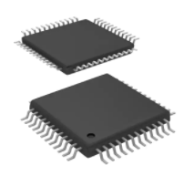
48-Pin TQFP Package
ESD Sensitive – HBM Capability of 500 V,
1000 V at All Input Pins
•
•
•
DWDM
Instrumentation
High-Speed, High-Resolution, Zero Latency
Data Acquisition Systems
Transducer Interface
Medical Instruments
Communication
DESCRIPTION
The ADS8411 is a 16-bit, 2 MHz A/D converter with
an internal 4.096-V reference. The device includes a
16-bit capacitor-based SAR A/D converter with inherent sample and hold. The ADS8411 offers a full
16-bit interface and an 8-bit option where data is read
using two 8-bit read cycles.
The ADS8411 has a unipolar single-ended input. It is
available in a 48-lead TQFP package and is
characterized over the industrial -40°C to 85°C temperature range.
SAR
+IN
−IN
+
_
Output
Latches
and
3-State
Drivers
CDAC
BYTE
16-/8-Bit
Parallel DATA
Output Bus
Comparator
RESET
REFIN
REFOUT
4.096-V
Internal
Reference
Clock
Conversion
and
Control Logic
CONVST
BUSY
CS
RD
Please be aware that an important notice concerning availability, standard warranty, and use in critical applications of Texas
Instruments semiconductor products and disclaimers thereto appears at the end of this data sheet.
PRODUCTION DATA information is current as of publication date.
Products conform to specifications per the terms of the Texas
Instruments standard warranty. Production processing does not
necessarily include testing of all parameters.
Copyright © 2002–2004, Texas Instruments Incorporated
�ADS8411
www.ti.com
SLAS369B – APRIL 2002 – REVISED DECEMBER 2004
This integrated circuit can be damaged by ESD. Texas Instruments recommends that all integrated
circuits be handled with appropriate precautions. Failure to observe proper handling and installation
procedures can cause damage.
ESD damage can range from subtle performance degradation to complete device failure. Precision
integrated circuits may be more susceptible to damage because very small parametric changes could
cause the device not to meet its published specifications.
ORDERING INFORMATION (1)
MODEL
ADS8411I
ADS8411IB
(1)
MAXIMUM
INTEGRAL
LINEARITY
(LSB)
–6 ~ 6
–2.5 ~ 2.5
MAXIMUM
DIFFERENTIAL
LINEARITY
(LSB)
NO MISSING
CODES
RESOLUTION
(BIT)
PACKAGE
TYPE
15
48 Pin
TQFP
–2~3
–1~2
16
48 Pin
TQFP
PACKAGE
DESIGNATOR
PFB
PFB
TEMPERATURE
RANGE
ORDERING
INFORMATION
TRANSPORT
MEDIA
QUANTITY
ADS8411IPFBT
Tape and reel
250
ADS8411IPFBR
Tape and reel
1000
ADS8411IBPFBT
Tape and reel
250
ADS8411IBPFBR
Tape and reel
1000
–40°C to 85°C
–40°C to 85°C
For the most current specifications and package information, refer to our website at www.ti.com.
ABSOLUTE MAXIMUM RATINGS
over operating free-air temperature range unless otherwise noted (1)
UNIT
Voltage
Voltage range
+IN to AGND
–0.4 V to +VA + 0.1 V
–IN to AGND
–0.4 V to 0.5 V
+VA to AGND
–0.3 V to 7 V
+VBD to BDGND
+VA to +VBD
–0.3 V to 7 V
–0.3 V to 2.55 V
Digital input voltage to BDGND
–0.3 V to +VBD + 0.3 V
Digital output voltage to BDGND
–0.3 V to +VBD + 0.3 V
TA
Operating free-air temperature range
–40°C to 85°C
Tstg
Storage temperature range
–65°C to 150°C
Junction temperature (TJ max)
TQFP package
Power dissipation
θJA thermal impedance
Lead temperature, soldering
(1)
2
150°C
(TJMax - TA)/θJA
86°C/W
Vapor phase (60 sec)
215°C
Infrared (15 sec)
220°C
Stresses beyond those listed under absolute maximum ratings may cause permanent damage to the device. These are stress ratings
only, and functional operation of the device at these or any other conditions beyond those indicated under recommended operating
conditions is not implied. Exposure to absolute-maximum-rated conditions for extended periods may affect device reliability.
�ADS8411
www.ti.com
SLAS369B – APRIL 2002 – REVISED DECEMBER 2004
SPECIFICATIONS
TA = –40°C to 85°C, +VA = 5 V, +VBD = 3 V or 5 V, Vref = 4.096 V, fSAMPLE = 2 MHz (unless otherwise noted)
PARAMETER
TEST CONDITIONS
MIN
TYP
MAX
UNIT
ANALOG INPUT
Full-scale input voltage
(1)
+IN – (–IN)
Absolute input voltage
0
Vref
+IN
–0.2
Vref + 0.2
–IN
–0.2
0.2
V
V
Input capacitance
25
pF
Input leakage current
0.5
nA
16
Bits
SYSTEM PERFORMANCE
Resolution
No missing codes
Integral linearity
DNL
Differential linearity
EO
Offset error (4)
16
ADS8411IB
–6
±4
6
–2.5
±1.5
2.5
LSB
–2
±1
3
ADS8411IB
–1
±0.8
2
–1.5
±0.5
1.5
mV
ADS8411IB
–0.75
±0.25
0.75
mV
ADS8411I
–0.15
0.15
–0.098
0.098
ADS8411IB
Noise
PSRR
Bits
ADS8411I
ADS8411I
Gain error (4) (5)
EG
15
ADS8411IB
ADS8411I
(2) (3)
INL
ADS8411I
DC Power supply rejection ratio
At FFFFh output code,
+VA = 4.75 V to 5.25 V,
Vref = 4.096 V (4)
LSB
%FS
60
µV RMS
2
LSB
SAMPLING DYNAMICS
Conversion time
340
Acquisition time
100
400
ns
ns
Throughput rate
2
MHz
Aperture delay
2
ns
Aperture jitter
25
ps
Step response
100
ns
Overvoltage recovery
100
ns
VIN = 4 Vpp at 100 kHz
–90
dB
DYNAMIC CHARACTERISTICS
(6)
THD
Total harmonic distortion
VIN = 4 Vpp at 500 kHz
–88.5
dB
SNR
Signal-to-noise ratio
VIN = 4 Vpp at 100 kHz
86
dB
SINAD
Signal-to-noise + distortion
VIN = 4 Vpp at 100 kHz
85
dB
SFDR
Spurious free dynamic range
VIN = 4 Vpp at 100 kHz
90
dB
VIN = 4 Vpp at 500 kHz
88
dB
5
MHz
-3dB Small signal bandwidth
EXTERNAL VOLTAGE REFERENCE INPUT
Reference voltage at REFIN, Vref
Reference resistance
(1)
(2)
(3)
(4)
(5)
(6)
(7)
(7)
3.9
4.096
500
4.2
V
kΩ
Ideal input span, does not include gain or offset error.
LSB means least significant bit
This is endpoint INL, not best fit.
Measured relative to an ideal full-scale input [+IN – (–IN)] of 4.096 V
This specification does not include the internal reference voltage error and drift.
Calculated on the first nine harmonics of the input frequency
Can vary ±20%
3
�ADS8411
www.ti.com
SLAS369B – APRIL 2002 – REVISED DECEMBER 2004
SPECIFICATIONS (continued)
TA = –40°C to 85°C, +VA = 5 V, +VBD = 3 V or 5 V, Vref = 4.096 V, fSAMPLE = 2 MHz (unless otherwise noted)
PARAMETER
TEST CONDITIONS
MIN
TYP
MAX
UNIT
120
ms
INTERNAL REFERENCE OUTPUT
Vref
Internal reference start-up time
From 95% (+VA), with 1
µF storage capacitor
Reference voltage
IOUT = 0
Source current
Static load
Line regulation
+VA = 4.75 ~ 5.25 V
0.6
mV
Drift
IOUT = 0
36
PPM/°C
4.065
4.096
4.13
V
10
µA
DIGITAL INPUT/OUTPUT
Logic family — CMOS
VIH
High level input voltage
IIH = 5 µA
+VBD – 1
VIL
Low level input voltage
IIL = 5 µA
–0.3
+VBD + 0.3
0.8
VOH
High level output voltage
IOH = 2 TTL loads
+VBD – 0.6
+VBD
VOL
Low level output voltage
IOL = 2 TTL loads
0
0.4
V
Data format — straight binary
POWER SUPPLY REQUIREMENTS
Power supply voltage
PD
+VBD
2.7
+VA
4.75
3
5.25
V
5
5.25
+VA Supply current (8)
fs = 2 MHz
35
38
mA
V
Power dissipation (8)
fs = 2 MHz
175
190
mW
85
°C
TEMPERATURE RANGE
TA
(8)
4
Operating free-air
–40
This includes only +VA current. +VBD current is typically 1 mA with 5-pF load capacitance on output pins.
�ADS8411
www.ti.com
SLAS369B – APRIL 2002 – REVISED DECEMBER 2004
TIMING CHARACTERISTICS
All specifications typical at –40°C to 85°C, +VA = +VBD = 5 V
(1) (2) (3)
PARAMETER
MIN
tCONV
Conversion time
340
tACQ
Acquisition time
100
tpd1
CONVST low to BUSY high
tpd2
Propagation delay time, end of conversion to BUSY low
tw1
Pulse duration, CONVST low
tsu1
Setup time, CS low to CONVST low
tw2
Pulse duration, CONVST high
TYP
MAX
UNIT
400
ns
ns
30
ns
5
ns
20
ns
0
ns
20
ns
CONVST falling edge jitter
10
tw3
Pulse duration, BUSY signal low
tw4
Pulse duration, BUSY signal high
th1
Hold time, first data bus data transition (RD low, or CS low for read
cycle, or BYTE input changes) after CONVST low
td1
tsu2
tw5
Pulse duration, RD low
ten
Enable time, RD low (or CS low for read cycle) to data valid
td2
Delay time, data hold from RD high
0
td3
Delay time, BYTE rising edge or falling edge to data valid
2
tw6
Pulse duration, RD high
20
ns
tw7
Pulse duration, CS high
20
ns
th2
Hold time, last RD (or CS for read cycle ) rising edge to CONVST
falling edge
50
ns
tsu3
Setup time, BYTE transition to RD falling edge
0
ns
th3
Hold time, BYTE transition to RD falling edge
0
tdis
Disable time, RD high (CS high for read cycle) to 3-stated data bus
20
ns
td5
Delay time, end of conversion to MSB data valid
10
ns
tsu4
Byte transition setup time, from BYTE transition to next BYTE
transition
50
ns
td6
Delay time, CS rising edge to BUSY falling edge
50
ns
td7
Delay time, BUSY falling edge to CS rising edge
50
ns
tsu(AB)
Setup time, from the falling edge of CONVST (used to start the valid
conversion) to the next falling edge of CONVST (when CS = 0 and
CONVST used to abort) or to the next falling edge of CS (when CS is
used to abort)
60
tsu5
Setup time, falling edge of CONVST to read valid data (MSB) from
current conversion
th4
Hold time, data (MSB) from previous conversion hold valid from
falling edge of CONVST
(1)
(2)
(3)
Min(tACQ)
ps
ns
370
ns
40
ns
Delay time, CS low to RD low (or BUSY low to RD low)
0
ns
Setup time, RD high to CS high
0
ns
50
ns
20
ns
ns
20
ns
ns
340
MAX(tCONV) + MAX(td5)
ns
ns
MIN(tCONV)
ns
All input signals are specified with tr = tf = 5 ns (10% to 90% of +VBD) and timed from a voltage level of (VIL + VIH)/2.
See timing diagrams.
All timings are measured with 20 pF equivalent loads on all data bits and BUSY pins.
5
�ADS8411
www.ti.com
SLAS369B – APRIL 2002 – REVISED DECEMBER 2004
TIMING CHARACTERISTICS
All specifications typical at –40°C to 85°C, +VA = 5 V, +VBD = 3 V (1) (2) (3)
PARAMETER
MIN
TYP
MAX
UNIT
400
ns
tCONV
Conversion time
340
tACQ
Acquisition time
100
tpd1
CONVST low to conversion started (BUSY high)
40
ns
tpd2
Propagation delay time, end of conversion to BUSY low
10
ns
tw1
Pulse duration, CONVST low
tsu1
Setup time, CS low to CONVST low
tw2
Pulse duration, CONVST high
ns
20
ns
0
ns
20
ns
CONVST falling edge jitter
10
tw3
Pulse duration, BUSY signal low
tw4
Pulse duration, BUSY signal high
th1
Hold time, first data bus transition (RD low, or CS low for read cycle,
or BYTE input changes) after CONVST low
td1
tsu2
tw5
Pulse duration, RD low
ten
Enable time, RD low (or CS low for read cycle) to data valid
td2
Delay time, data hold from RD high
0
td3
Delay time, BYTE rising edge or falling edge to data valid
2
tw6
Pulse duration, RD high
20
ns
tw7
Pulse duration, CS high
20
ns
th2
Hold time, last RD (or CS for read cycle ) rising edge to CONVST
falling edge
50
ns
tsu3
Setup time, BYTE transition to RD falling edge
0
ns
th3
Hold time, BYTE transition to RD falling edge
0
tdis
Disable time, RD high (CS high for read cycle) to 3-stated data bus
30
ns
td5
Delay time, end of conversion to MSB data valid
20
ns
tsu4
Byte transition setup time, from BYTE transition to next BYTE
transition
50
ns
td6
Delay time, CS rising edge to BUSY falling edge
50
ns
td7
Delay time, BUSY falling edge to CS rising edge
50
ns
tsu(AB)
Setup time, from the falling edge of CONVST (used to start the valid
conversion) to the next falling edge of CONVST (when CS = 0 and
CONVST used to abort) or to the next falling edge of CS (when CS is
used to abort)
70
tsu5
Setup time, falling edge of CONVST to read valid data (MSB) from
current conversion
th4
Hold time, data (MSB) from previous conversion hold valid from
falling edge of CONVST
(1)
(2)
(3)
6
Min(tACQ)
ps
ns
370
ns
40
ns
Delay time, CS low to RD low (or BUSY low to RD low)
0
ns
Setup time, RD high to CS high
0
ns
50
ns
30
ns
ns
30
ns
ns
350
MAX(tCONV) + MAX(td5)
ns
ns
MIN(tCONV)
All input signals are specified with tr = tf = 5 ns (10% to 90% of +VBD) and timed from a voltage level of (VIL + VIH)/2.
See timing diagrams.
All timings are measured with 20 pF equivalent loads on all data bits and BUSY pins.
ns
�ADS8411
www.ti.com
SLAS369B – APRIL 2002 – REVISED DECEMBER 2004
PIN ASSIGNMENTS
BUSY
BDGND
+VBD
DB0
DB1
DB2
DB3
DB4
DB5
DB6
DB7
BDGND
PFB PACKAGE
(TOP VIEW)
36 35 34 33 32 31 30 29 28 27 26 25
37
24
38
23
39
22
40
21
41
20
42
19
43
18
44
17
45
16
46
15
47
14
48
3
4 5
6 7 8
13
9 10 11 12
REFIN
REFOUT
NC
+VA
AGND
+IN
-IN
AGND
+VA
+VA
1 2
+VBD
DB8
DB9
DB10
DB11
DB12
DB13
DB14
DB15
AGND
AGND
+VA
AGND
AGND
+VBD
RESET
BYTE
CONVST
RD
CS
+VA
AGND
AGND
+VA
REFM
REFM
NC - No connection
7
�ADS8411
www.ti.com
SLAS369B – APRIL 2002 – REVISED DECEMBER 2004
Terminal Functions
NAME
NO.
I/O
AGND
5, 8, 11, 12, 14,
15, 44, 45
–
Analog ground
BDGND
DESCRIPTION
25, 35
–
Digital ground for bus interface digital supply
BUSY
36
O
Status output. High when a conversion is in progress.
BYTE
39
I
Byte select input. Used for 8-bit bus reading. 0: No fold back 1: Low byte D[7:0] of the 16 most
significant bits is folded back to high byte of the 16 most significant pins DB[15:8].
CONVST
40
I
Convert start. The falling edge of this input ends the acquisition period and starts the hold
period.
CS
42
I
Chip select. The falling edge of this input starts the acquisition period.
8-Bit Bus
Data Bus
16-Bit Bus
BYTE = 0
BYTE = 1
BYTE = 0
DB15
16
O
D15 (MSB)
D7
D15 (MSB)
DB14
17
O
D14
D6
D14
DB13
18
O
D13
D5
D13
DB12
19
O
D12
D4
D12
DB11
20
O
D11
D3
D11
DB10
21
O
D10
D2
D10
DB9
22
O
D9
D1
D9
DB8
23
O
D8
D0 (LSB)
D8
DB7
26
O
D7
All ones
D7
DB6
27
O
D6
All ones
D6
DB5
28
O
D5
All ones
D5
DB4
29
O
D4
All ones
D4
DB3
30
O
D3
All ones
D3
DB2
31
O
D2
All ones
D2
DB1
32
O
D1
All ones
D1
DB0
33
O
D0 (LSB)
All ones
D0 (LSB)
–IN
7
I
Inverting input channel
+IN
6
I
Non inverting input channel
NC
3
–
No connection
REFIN
1
I
Reference input
REFM
47, 48
I
Reference ground
REFOUT
2
O
Reference output. Add 1 µF capacitor between the REFOUT pin and REFM pin when internal
reference is used.
RESET
38
I
Current conversion is aborted and output latches are cleared (set to zeros) when this pin is
asserted low. RESET works independantly of CS.
RD
41
I
Synchronization pulse for the parallel output. When CS is low, this serves as the output enable
and puts the previous conversion result on the bus.
+VA
4, 9, 10, 13, 43,
46
–
Analog power supplies, 5-V dc
24, 34, 37
–
Digital power supply for bus
+VBD
8
�ADS8411
www.ti.com
SLAS369B – APRIL 2002 – REVISED DECEMBER 2004
TIMING DIAGRAMS
tw2
tw1
CONVST
(used in normal
conversion)
tcycle
CONVST
(used in ABORT)
tsu(AB)
tpd1
tsu(AB)
tpd2
tw4
tpd1
tw3
BUSY
tsu1
tw7
td7
CS
td6
CONVERT†
tCONV
tCONV
SAMPLING†
(When CS Toggle)
tACQ
BYTE
tsu4
th1
tsu2
td1
th2
RD
Data to
be read†
Invalid
Previous Conversion
th4
tdis
ten
tsu5
DB[15:8]
Invalid
Current Conversion
Hi−Z
Hi−Z
D [15:8]
DB[7:0]
Hi−Z
D [7:0]
Hi−Z
D [7:0]
†Signal
internal to device
Figure 1. Timing for Conversion and Acquisition Cycles With CS and RD Toggling
9
�ADS8411
www.ti.com
SLAS369B – APRIL 2002 – REVISED DECEMBER 2004
TIMING DIAGRAMS (continued)
tw1
CONVST
(used in normal
conversion)
tw2
tcycle
CONVST
(used in ABORT)
tsu(AB)
tpd1
tsu(AB)
tpd2
tw4
tw3
BUSY
tw7
tsu1
td7
CS
td6
CONVERT†
tCONV
tCONV
SAMPLING†
(When CS Toggle)
tACQ
BYTE
th1
RD = 0
Data to
be read†
tdis
ten
DB[15:8]
DB[7:0]
†Signal
Invalid
Current Conversion
tsu5
Hi−Z
Previous
D [15:8]
Hi−Z
Hi−Z
Previous
D [7:0]
Hi−Z
internal to device
tdis
Invalid
Previous Conversion
th4
tsu4
th2
ten
D [15:8]
D [7:0]
D [7:0]
Hi−Z
Repeated
D [15:8]
Hi−Z
Repeated
D [7:0]
ten
Figure 2. Timing for Conversion and Acquisition Cycles With CS Toggling, RD Tied to BDGND
10
�ADS8411
www.ti.com
SLAS369B – APRIL 2002 – REVISED DECEMBER 2004
TIMING DIAGRAMS (continued)
tw1
tw2
CONVST
(used in normal
conversion)
tcycle
CONVST
(used in ABORT)
tsu(AB)
tpd1
tsu(AB)
tpd2
tw4
tpd1
tw3
BUSY
CS = 0
CONVERT†
tCONV
tCONV
t(ACQ)
SAMPLING†
(When CS = 0)
BYTE
tsu4
th1
th2
RD
tdis
ten
Data to
be read†
th4
DB[15:8]
DB[7:0]
†Signal
Invalid
Invalid
Previous Conversion
Current Conversion
tsu5
Hi−Z
Hi−Z
D [15:8]
D [7:0]
D [7:0]
Hi−Z
Hi−Z
internal to device
Figure 3. Timing for Conversion and Acquisition Cycles With CS Tied to BDGND, RD Toggling
11
�ADS8411
www.ti.com
SLAS369B – APRIL 2002 – REVISED DECEMBER 2004
TIMING DIAGRAMS (continued)
tw1
CONVST
(used in normal
conversion)
tw2
tcycle
CONVST
(used in ABORT)
tsu(AB)
tpd1
tsu(AB)
tpd2
tw4
tpd1
tpd2
tw3
BUSY
CS = 0
CONVERT†
tCONV
tCONV
tACQ
SAMPLING†
(When CS Toggle)
th1
th1
BYTE
RD = 0
td3
td3
td5
th4
tsu5
Previous
MSB
Invalid
DB[15:8]
Previous Previous
LSB
LSB
Invalid
DB[7:0]
†Signal
td5
th4
td3
tsu5
Invalid
MSB
LSB
MSB
MSB
LSB
MSB
Invalid
internal to device
Figure 4. Timing for Conversion and Acquisition Cycles With CS and RD Tied to BDGND—Auto Read
CS
RD
tsu4
BYTE
ten
tdis
tdis
ten
DB[15:0]
td3
Hi−Z
Valid
Hi−Z
Valid
Valid
Figure 5. Detailed Timing for Read Cycles
12
Hi−Z
�ADS8411
www.ti.com
SLAS369B – APRIL 2002 – REVISED DECEMBER 2004
TYPICAL CHARACTERISTICS
At –40°C to 85°C, +VA = 5 V, +VBD = 5 V, REFIN = 4.096 V (internal reference used) and fsample = 2 MHz
(unless otherwise noted)
HISTOGRAM (DC CODE SPREAD)
vs
FULL SCALE 131071 CONVERSIONS
SIGNAL-TO-NOISE RATIO
vs
FREE-AIR TEMPERATURE
70000
86.8
+VA = 5 V,
+VBD = 3.3 V
Code = 65235
86.6
SNR − Signal-to-Noise Ratio − dB
60000
50000
40000
30000
20000
10000
86.4
86.2
86
85.8
85.6
85.4
85.2
−40
65239
65235
65230
0
0
20
40
60
TA − Free-Air Temperature − °C
Figure 7.
SIGNAL-TO-NOISE AND DISTORTION
vs
FREE-AIR TEMPERATURE
EFFECTIVE NUMBER OF BITS
vs
FREE-AIR TEMPERATURE
80
13.6
83.4
83.2
83
ENOB − Effective Number of Bits − Bits
fi = 100 kHz,
+VA = 5 V,
+VBD = 3.3 V,
TA = 25°C,
Internal
Reference
83.6
82.8
82.6
82.4
82.2
82
81.8
81.6
−40
−20
Figure 6.
83.8
SINAD − Signal-to-Nois and Distortion − dB
fi = 100 kHz,
+VA = 5 V,
+VBD = 3.3 V,
TA = 25°C,
Internal
Reference
−20
0
20
40
60
TA − Free-Air Temperature − °C
Figure 8.
80
fi = 100 kHz,
+VA = 5 V,
+VBD = 3.3 V,
TA = 25°C,
Internal
Reference
13.55
13.5
13.45
13.4
13.35
13.3
13.25
−40
−20
0
20
40
60
TA − Free-Air Temperature − °C
80
Figure 9.
13
�ADS8411
www.ti.com
SLAS369B – APRIL 2002 – REVISED DECEMBER 2004
TYPICAL CHARACTERISTICS (continued)
SPURIOUS FREE DYNAMIC RANGE
vs
FREE-AIR TEMPERATURE
TOTAL HARMONIC DISTORTION
vs
FREE-AIR TEMPERATURE
−91
fi = 100 kHz,
+VA = 5 V,
+VBD = 3.3 V,
TA = 25°C,
Internal
Reference
95
94.5
THD − Total Harmonic Distortion − dB
SFDR − Spurious Free Dynamic Range − dB
95.5
94
93.5
93
92.5
92
−40
−20
0
20
40
60
TA − Free-Air Temperature − °C
−92.5
−93
−93.5
−94
−20
0
20
40
60
80
TA − Free-Air Temperature − °C
Figure 10.
Figure 11.
SIGNAL-TO-NOISE RATIO
vs
INPUT FREQUENCY
EFFECTIVE NUMBER OF BITS
vs
INPUT FREQUENCY
13.9
86.7
ENOB − Effective Number of Bits − Bits
+VA = 5 V,
+VBD = 3.3 V,
TA = 25°C,
Internal
Reference
86.8
SNR − Signal-to-Noise Ratio − dB
−92
−94.5
−40
80
86.9
86.6
86.5
86.4
86.3
86.2
86.1
86
0
20
40
60
80
fi − Input Frequency − kHz
Figure 12.
14
−91.5
fi = 100 kHz,
+VA = 5 V,
+VBD = 3.3 V,
TA = 25°C,
Internal
Reference
100
+VA = 5 V,
+VBD = 3.3 V,
TA = 25°C,
Internal
Reference
13.85
13.8
13.75
13.7
13.65
13.6
13.55
13.5
13.45
13.4
0
20
40
60
80
fi − Input Frequency − kHz
Figure 13.
100
�ADS8411
www.ti.com
SLAS369B – APRIL 2002 – REVISED DECEMBER 2004
TYPICAL CHARACTERISTICS (continued)
SIGNAL-TO-NOISE AND DISTORTION
vs
INPUT FREQUENCY
SPURIOUS FREE DYNAMIC RANGE
vs
INPUT FREQUENCY
103
+VA = 5 V,
+VBD = 3.3 V,
TA = 25°C,
Internal
Reference
85
SFDR − Spurious Free Dynamic Range − dB
SINAD − Signal-to-Nois and Distortion − dB
85.50
84.50
84
83.50
83
82.50
0
20
40
60
80
101
100
99
98
97
96
95
94
100
+VA = 5 V,
+VBD = 3.3 V,
TA = 25°C,
Internal
Reference
102
0
20
fi − Input Frequency − kHz
Figure 14.
Figure 15.
TOTAL HARMONIC DISTORTION
vs
INPUT FREQUENCY
SUPPLY CURRENT
vs
SAMPLE RATE
−94
100
33.5
+VA = 5 V,
+VBD = 3.3 V,
TA = 25°C,
Internal
Reference
33
ICC − Supply Current − mA
THD − Total Harmonic Distortion − dB
−92
−93
40
60
80
fi − Input Frequency − kHz
−95
−96
−97
−98
−99
32.5
32
+VA = 5 V,
+VBD = 3.3 V,
TA = 25°C,
Internal
Reference
31.5
31
30.5
30
29.5
−100
29
−101
0
20
40
60
80
fi − Input Frequency − kHz
Figure 16.
100
28.5
500
700
900
1100 1300 1500 1700 1900
Samply Rate − KSPS
Figure 17.
15
�ADS8411
www.ti.com
SLAS369B – APRIL 2002 – REVISED DECEMBER 2004
TYPICAL CHARACTERISTICS (continued)
GAIN ERROR
vs
SUPPLY VOLTAGE
OFFSET ERROR
vs
SUPPLY VOLTAGE
0.45
0.25
+VBD = 3.3 V,
TA = 25°C,
External
Reference
0.35
EO − Offset Error − mV
E G − Gain Error − mV
0.20
+VB D= 3.3 V,
TA = 25°C,
External
Reference
0.40
0.15
0.10
0.30
0.25
0.20
0.15
0.10
0.05
0.05
0
4.75
4.85
4.95
5.05
5.15
VDD − Supply Voltage − V
0
4.75
5.25
Figure 18.
Figure 19.
INTERNAL VOLTAGE REFERENCE
vs
FREE-AIR TEMPERATURE
GAIN ERROR
vs
FREE-AIR TEMPERATURE
+VA = 5 V,
+VBD = 3.3 V
5.25
+VA = 5 V,
+VBD = 3.3 V,
External
Reference
0.30
0.25
4.090
E G − Gain Error − mV
Internal Voltage Reference − V
4.091
4.089
4.088
4.087
4.086
0.20
0.15
0.10
0.05
0
4.085
−0.05
4.084
−0.10
−20
0
20
40
60
TA − Free-Air Temperature − °C
Figure 20.
16
5.15
0.35
4.092
4.083
−40
4.85
4.95
5.05
VDD − Supply Voltage − V
80
−0.15
−40
−20
0
20
40
60
TA − Free-Air Temperature − °C
Figure 21.
80
�ADS8411
www.ti.com
SLAS369B – APRIL 2002 – REVISED DECEMBER 2004
TYPICAL CHARACTERISTICS (continued)
OFFSET ERROR
vs
FREE-AIR TEMPERATURE
0.5
33.6
+VA = 5 V,
+VBD = 3.3 V,
External
Reference
0.3
0.2
0.1
0
−0.1
33
32.8
32.6
32.4
−0.3
32.2
−20
0
20
40
60
TA − Free-Air Temperature − °C
32
−40
80
Figure 23.
DIFFERENTIAL NONLINEARITY
vs
FREE-AIR TEMPERATURE
INTEGRAL NONLINEARITY
vs
FREE-AIR TEMPERATURE
INL − Integral Nonlinearity − LSBs
Max
1
0
80
2.5
1.5
0.5
−20
0
20
40
60
TA − Free-Air Temperature − °C
Figure 22.
2
DNL − Differential Nonlinearity − LSBs
33.2
−0.2
−0.4
−40
+VA = 5 V,
+VBD = 3.3 V
33.4
ICC − Supply Current − mA
0.4
EO − Offset Error − mV
SUPPLY CURRENT
vs
FREE-AIR TEMPERATURE
+VA = 5 V,
+VBD = 3.3 V,
Internal
Reference
−0.5
Min
−1
2
1.5
MAX
1
0.5
0
−0.5
MIN
−1
−1.5
−2
−1.5
−40
−20
0
20
40
60
TA − Free-Air Temperature − °C
Figure 24.
80
−2.5
−40
−25
−10
5
20
35
50
65
80
TA − Free-Air Temperature − °C
Figure 25.
17
�ADS8411
www.ti.com
SLAS369B – APRIL 2002 – REVISED DECEMBER 2004
TYPICAL CHARACTERISTICS (continued)
DNL
4
3
DNL − LSBs
2
1
0
−1
−2
−3
−4
0
32768
Code
Figure 26.
16384
49152
65536
49152
65536
INL
4
3
INL − LSBs
2
1
0
−1
−2
−3
−4
0
32768
Code
Figure 27.
16384
FFT
Magnitude − dB
0
−20
−40
−60
−80
−100
−120
−140
−160
−180
0
100
200
300
400
500
600
Frequency − kHz
Figure 28.
18
700
800
900
1000
�ADS8411
www.ti.com
SLAS369B – APRIL 2002 – REVISED DECEMBER 2004
APPLICATION INFORMATION
MICROCONTROLLER INTERFACING
ADS8411 to 8-Bit Microcontroller Interface
Figure 29 shows a parallel interface between the ADS8411 and a typical microcontroller using the 8-bit data bus.
The BUSY signal is used as a falling-edge interrupt to the microcontroller.
Analog 5 V
0.1 µF
AGND
10 µF
Ext Ref Input
0.1 µF
1 µF
Micro
Controller
-IN
REFM
AGND
+IN
+VA
REFIN
Analog Input
Digital 3 V
ADS8411
GPIO
CS
GPIO
P[7:0]
BYTE
DB[15:8]
RD
CONVST
BUSY
RD
GPIO
INT
0.1 µF
BDGND
BDGND
+VBD
Figure 29. ADS8411 Application Circuitry (using external reference)
Analog 5 V
0.1 µF
AGND
10 µF
0.1 µF
AGND
AGND
REFM
REFIN
REFOUT
+VA
1 µF
ADS8411
Figure 30. Use Internal Reference
PRINCIPLES OF OPERATION
The ADS8411 is a high-speed successive approximation register (SAR) analog-to-digital converter (ADC). The
architecture is based on charge redistribution, which inherently includes a sample/hold function. See Figure 29
for the application circuit for the ADS8411.
The conversion clock is generated internally. The conversion time of 400 ns is capable of sustaining a 2-MHz
throughput.
19
�ADS8411
SLAS369B – APRIL 2002 – REVISED DECEMBER 2004
www.ti.com
PRINCIPLES OF OPERATION (continued)
The analog input is provided to two input pins: +IN and –IN. When a conversion is initiated, the differential input
on these pins is sampled on the internal capacitor array. While a conversion is in progress, both inputs are
disconnected from any internal function.
REFERENCE
The ADS8411 can operate with an external reference with a range from 3.9 V to 4.2 V. A 4.096-V internal
reference is included. When the internal reference is used, pin 2 (REFOUT) should be connected to pin 1
(REFIN) with 0.1-µF decoupling capacitor and 1-µF storage capacitor between pin 2 (REFOUT) and pins 47 and
48 (REFM) (see Figure 30). The internal reference of the converter is double buffered. If an external reference is
used, the second buffer provides isolation between the external reference and the CDAC. This buffer is also
used to recharge all of the capacitors of the CDAC during conversion. Pin 2 (REFOUT) can be left unconnected
(floating) if an external reference is used.
ANALOG INPUT
When the converter enters the hold mode, the voltage difference between the +IN and -IN inputs is captured on
the internal capacitor array. The voltage on the –IN input is limited between –0.2 V and 0.2 V, allowing the input
to reject small signals which are common to both the +IN and –IN inputs. The +IN input has a range of –0.2 V to
Vref + 0.2 V. The input span (+IN – (–IN)) is limited to 0 V to Vref.
The input current on the analog inputs depends upon a number of factors: sample rate, input voltage, and source
impedance. Essentially, the current into the ADS8411 charges the internal capacitor array during the sample
period. After this capacitance has been fully charged, there is no further input current. The source of the analog
input voltage must be able to charge the input capacitance (25 pF) to an 16-bit settling level within the acquisition
time (100 ns) of the device. When the converter goes into the hold mode, the input impedance is greater than 1
GΩ.
Care must be taken regarding the absolute analog input voltage. To maintain the linearity of the converter, the
+IN and –IN inputs and the span (+IN – (–IN)) should be within the limits specified. Outside of these ranges, the
converter's linearity may not meet specifications. To minimize noise, low bandwidth input signals with low-pass
filters should be used.
Care should be taken to ensure that the output impedance of the sources driving +IN and –IN inputs are
matched. If this is not observed, the two inputs could have different setting time. This may result in offset error,
gain error and linearity error which varies with temperature and input voltage.
DIGITAL INTERFACE
Timing And Control
See the timing diagrams in the specifications section for detailed information on timing signals and their
requirements.
The ADS8411 uses an internal oscillator generated clock which controls the conversion rate and in turn the
throughput of the converter. No external clock input is required.
Conversions are initiated by bringing the CONVST pin low for a minimum of 20 ns (after the 20 ns minimum
requirement has been met, the CONVST pin can be brought high), while CS is low. The ADS8411 switches from
the sample to the hold mode on the falling edge of the CONVST command. A clean and low jitter falling edge of
this signal is important to the performance of the converter. The BUSY output is brought high after CONVST
goes low. BUSY stays high throughout the conversion process and returns low when the conversion has ended.
Sampling starts with the falling edge of the BUSY signal when CS is tied low or starts with the falling edge of CS
when BUSY is low.
Both RD and CS can be high during and before a conversion with one exception (CS must be low when
CONVST goes low to initiate a conversion). Both the RD and CS pins are brought low in order to enable the
parallel output bus with the conversion.
20
�ADS8411
www.ti.com
SLAS369B – APRIL 2002 – REVISED DECEMBER 2004
PRINCIPLES OF OPERATION (continued)
Reading Data
The ADS8411 outputs full parallel data in straight binary format as shown in Table 1. The parallel output is active
when CS and RD are both low. There is a minimal quiet zone requirement around the falling edge of CONVST.
This is 50 ns prior to the falling edge of CONVST and 40 ns after the falling edge. No data read should be
attempted within this zone. Any other combination of CS and RD sets the parallel output to 3-state. BYTE is used
for multiword read operations. BYTE is used whenever lower bits of the converter result are output on the higher
byte of the bus. Refer to Table 1 for ideal output codes.
Table 1. Ideal Input Voltages and Output Codes
DESCRIPTION
ANALOG VALUE
DIGITAL OUTPUT
Full scale range
Vref
STRAIGHT BINARY
Least significant bit (LSB)
Vref/65536
Full scale
Vref– 1 LSB
1111 1111 1111 1111
FFFF
Midscale
Vref/2
1000 0000 0000 0000
8000
Midscale – 1 LSB
Vref/2 – 1 LSB
0111 1111 1111 1111
7FFF
Zero
0V
0000 0000 0000 0000
0000
BINARY CODE
HEX CODE
The output data is a full 16-bit word (D15–D0) on DB15–DB0 pins (MSB-LSB) if BYTE is low.
The result may also be read on an 8-bit bus for convenience. This is done by using only pins DB15-DB8. In this
case two reads are necessary: the first as before, leaving BYTE low and reading the 8 most significant bits on
pins DB15-DB8, then bringing BYTE high. When BYTE is high, the low bits (D7–D0) appear on pins DB15–D8.
These multiword read operations can be done with multiple active RD (toggling) or with RD tied low for simplicity.
Table 2. Conversion Data Readout
BYTE
DATA READ OUT
DB15–DB8 Pins
DB7-DB0 Pins
High
D7–D0
All one's
Low
D15–D8
D7-D0
RESET
RESET is an asynchronous active low input signal (that works independently of CS). Minimum RESET low time
is 25 ns. Current conversion will be aborted no later than 50 ns after the converter is in the reset mode. In
addition, all output latches are cleared (set to zero's) after RESET. The converter goes back to normal operation
mode no later than 20 ns after RESET input is brought high.
The converter starts the first sampling period 20 ns after the rising edge of RESET. Any sampling period except
for the one immediately after a RESET is started with the falling edge of the previous BUSY signal or the falling
edge of CS, whichever is later.
Another way to reset the device is through the use of the combination of CS and CONVST. This is useful when
the dedicated RESET pin is tied to the system reset but there is a need to abort only the conversion in a specific
converter. Since the BUSY signal is held high during the conversion, either one of these conditions triggers an
internal self-clear reset to the converter just the same as a reset via the dedicated RESET pin. The reset does
not have to be cleared as for the dedicated RESET pin. A reset can be started with either of the two following
steps.
• Issue a CONVST when CS is low and a conversion is in progress. The falling edge of CONVST must satisfy
the timing as specified by the timing parameter tsu(AB) mentioned in the timing characteristics table to ensure
a reset. The falling edge of CONVST starts a reset. Timing is the same as a reset using the dedicated
RESET pin except the instance of the falling edge is replaced by the falling edge of CONVST.
• Issue a CS while a conversion is in progress. The falling edge of CS must satisfy the timing as specified by
the timing parameter tsu(AB) mentioned in the timing characteristics table to ensure a reset.The falling edge of
CS causes a reset. Timing is the same as a reset using the dedicated RESET pin except the instance of the
falling edge is replaced by the falling edge of CS.
21
�ADS8411
www.ti.com
SLAS369B – APRIL 2002 – REVISED DECEMBER 2004
POWER-ON INITIALIZATION
RESET is not required after power on. An internal power-on-reset circuit generates the reset. To ensure that all
of the registers are cleared, the three conversion cycles must be given to the converter after power on.
LAYOUT
For optimum performance, care should be taken with the physical layout of the ADS8411 circuitry.
As the ADS8411 offers single-supply operation, it is often used in close proximity with digital logic,
microcontrollers, microprocessors, and digital signal processors. The more digital logic present in the design and
the higher the switching speed, the more difficult it is to achieve good performance from the converter.
The basic SAR architecture is sensitive to glitches or sudden changes on the power supply, reference, ground
connections and digital inputs that occur just prior to latching the output of the analog comparator. Thus, driving
any single conversion for an n-bit SAR converter, there are at least n windows in which large external transient
voltages can affect the conversion result. Such glitches might originate from switching power supplies, nearby
digital logic, or high power devices.
The degree of error in the digital output depends on the reference voltage, layout, and the exact timing of the
external event.
On average, the ADS8411 draws very little current from an external reference, as the reference voltage is
internally buffered. If the reference voltage is external and originates from an op amp, make sure that it can drive
the bypass capacitor or capacitors without oscillation. A 0.1-µF bypass capacitor and a 1-µF storage capacitor
are recommended from pin 1 (REFIN) directly to pin 48 (REFM). REFM and AGND should be shorted on the
same ground plane under the device.
The AGND and BDGND pins should be connected to a clean ground point. In all cases, this should be the
analog ground. Avoid connections which are close to the grounding point of a microcontroller or digital signal
processor. If required, run a ground trace directly from the converter to the power supply entry point. The ideal
layout consists of an analog ground plane dedicated to the converter and associated analog circuitry.
As with the AGND connections, +VA should be connected to a 5-V power supply plane or trace that is separate
from the connection for digital logic until they are connected at the power entry point. Power to the ADS8411
should be clean and well bypassed. A 0.1-µF ceramic bypass capacitor should be placed as close to the device
as possible. See Table 3 for the placement of the capacitor. In addition, a 1-µF to 10-µF capacitor is
recommended. In some situations, additional bypassing may be required, such as a 100-µF electrolytic capacitor
or even a Pi filter made up of inductors and capacitors—all designed to essentially low-pass filter the 5-V supply,
removing the high frequency noise.
Table 3. Power Supply Decoupling Capacitor Placement
POWER SUPPLY PLANE
SUPPLY PINS
CONVERTER ANALOG SIDE
CONVERTER DIGITAL SIDE
Pin pairs that require shortest path to decoupling capacitors
(4,5), (8,9), (10,11), (13,15),
(43,44), (45,46)
(24,25), (34, 35)
Pins that require no decoupling
12, 14
37
22
�PACKAGE OPTION ADDENDUM
www.ti.com
6-Feb-2020
PACKAGING INFORMATION
Orderable Device
Status
(1)
Package Type Package Pins Package
Drawing
Qty
Eco Plan
Lead/Ball Finish
MSL Peak Temp
(2)
(6)
(3)
Op Temp (°C)
Device Marking
(4/5)
ADS8411IBPFBR
ACTIVE
TQFP
PFB
48
1000
Green (RoHS
& no Sb/Br)
NIPDAU
Level-2-260C-1 YEAR
-40 to 85
ADS8411I
B
ADS8411IBPFBT
ACTIVE
TQFP
PFB
48
250
Green (RoHS
& no Sb/Br)
NIPDAU
Level-2-260C-1 YEAR
-40 to 85
ADS8411I
B
ADS8411IPFBT
ACTIVE
TQFP
PFB
48
250
Green (RoHS
& no Sb/Br)
NIPDAU
Level-2-260C-1 YEAR
-40 to 85
ADS8411I
(1)
The marketing status values are defined as follows:
ACTIVE: Product device recommended for new designs.
LIFEBUY: TI has announced that the device will be discontinued, and a lifetime-buy period is in effect.
NRND: Not recommended for new designs. Device is in production to support existing customers, but TI does not recommend using this part in a new design.
PREVIEW: Device has been announced but is not in production. Samples may or may not be available.
OBSOLETE: TI has discontinued the production of the device.
(2)
RoHS: TI defines "RoHS" to mean semiconductor products that are compliant with the current EU RoHS requirements for all 10 RoHS substances, including the requirement that RoHS substance
do not exceed 0.1% by weight in homogeneous materials. Where designed to be soldered at high temperatures, "RoHS" products are suitable for use in specified lead-free processes. TI may
reference these types of products as "Pb-Free".
RoHS Exempt: TI defines "RoHS Exempt" to mean products that contain lead but are compliant with EU RoHS pursuant to a specific EU RoHS exemption.
Green: TI defines "Green" to mean the content of Chlorine (Cl) and Bromine (Br) based flame retardants meet JS709B low halogen requirements of