�������
�� ��
�����
�
� � ��� ������� ���
ADS8472
SLAS514 – DECEMBER 2006
16-BIT, 1-MSPS, PSEUDO-BIPOLAR, FULLY DIFFERENTIAL INPUT, MICROPOWER
SAMPLING ANALOG-TO-DIGITAL CONVERTER WITH PARALLEL INTERFACE,
REFERENCE
FEATURES
•
•
•
•
•
•
•
•
•
•
•
•
•
•
•
•
•
•
APPLICATIONS
• Medical Instruments
0 to 1-MHz Sample Rate
• Optical Networking
±0.4 LSB Typ, ±0.65 LSB Max INL
• Transducer Interface
±0.3 LSB Typ, ±0.5 LSB Max DNL
• High Accuracy Data Acquisition Systems
16-Bit NMC Ensured Over Temperature
• Magnetometers
±0.1-mV Offset Error
±0.05-PPM/°C Offset Error Drift
DESCRIPTION
±0.035 %FSR Gain Error
The ADS8472 is an 16-bit, 1-MSPS A/C converter
±0.4-PPM/°C Gain Error Drift
with an internal 4.096-V reference and a
95dB SNR, -120dB THD, 123dB SFDR
pseudo-bipolar, fully differential input. The device
includes a 16-bit capacitor-based SAR A/D converter
Zero Latency
with inherent sample and hold. The ADS8472 offers
Low Power: 225 mW at 1 MSPS
a full 16-bit interface or an 8-bit bus option using two
Unipolar Differential Input Range: Vref to –Vref
read cycles.
Onboard Reference with 6 PPM/°C Drift
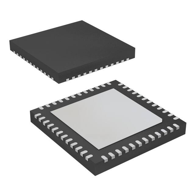
The ADS8472 is available in a 48-lead 7x7 QFN
Onboard Reference Buffer
package and is characterized over the industrial
–40°C to 85°C temperature range.
High-Speed Parallel Interface
Wide Digital Supply 2.7 V to 5.25 V
8-/16-Bit Bus Transfer
48-Pin 7x7 QFN Package
HIGH SPEED SAR CONVERTER FAMILY
TYPE/SPEED
500 kHz
~600 kHz
ADS8383
ADS8381
750 kHz
1 MHz
1.25 MHz
2 MHz
3 MHz
4MHz
ADS8481
18-Bit Pseudo-Diff
ADS8380 (s)
18-Bit Pseudo-Bipolar, Fully Diff
ADS8382 (s)
ADS8327
ADS8370 (s)
ADS8328
ADS8372 (s)
ADS8482
ADS8371
ADS8471
ADS8401
ADS8411
ADS8405
ADS8410 (s)
16-Bit Pseudo-Diff
ADS8472
ADS8402
ADS8412
ADS8406
ADS8413 (s)
ADS8422
16-Bit Pseudo-Bipolar, Fully Diff
14-Bit Pseudo-Diff
ADS7890 (s)
12-Bit Pseudo-Diff
ADS7886
SAR
+IN
−IN
+
_
CDAC
ADS7891
ADS7883
Output
Latches
and
3-State
Drivers
ADS7881
BYTE
16-/8-Bit
Parallel DA TA
Output Bus
Comparator
REFIN
REFOUT
4.096-V
Internal
Reference
Clock
Conversion
and
Control Logic
CONVST
BUSY
CS
RD
Please be aware that an important notice concerning availability, standard warranty, and use in critical applications of Texas
Instruments semiconductor products and disclaimers thereto appears at the end of this data sheet.
PRODUCTION DATA information is current as of publication date.
Products conform to specifications per the terms of the Texas
Instruments standard warranty. Production processing does not
necessarily include testing of all parameters.
Copyright © 2006, Texas Instruments Incorporated
�ADS8472
www.ti.com
SLAS514 – DECEMBER 2006
ORDERING INFORMATION (1)
MODEL
MAXIMUM
INTEGRAL
LINEARITY
(LSB)
MAXIMUM
DIFFERENTIAL
LINEARITY (LSB)
NO MISSING CODES
RESOLUTION (BIT)
PACKAGE
TYPE
PACKAGE
DESIGNATOR
TEMPER-ATURE
RANGE
ADS8472I
±1
±0.75
16
7x7 48 Pin
QFN
RGZ
–40°C to 85°C
ADS8472IB
(1)
±0.65
±0.5
16
7x7 48 Pin
QFN
RGZ
ORDERING
INFORMATION
TRANS-PORT
MEDIA QTY.
ADS8472IRGZT
Tape and reel
250
ADS8472IRGZR
Tape and reel
1000
ADS8472IBRGZT
Tape and reel
250
ADS8472IBRGZR
Tape and reel
1000
–40°C to 85°C
For the most current package and ordering information, see the Package Option Addendum at the end of this document, or see the TI
website at www.ti.com.
ABSOLUTE MAXIMUM RATINGS (1)
over operating free-air temperature range (unless otherwise noted)
Voltage
VALUE
UNIT
+IN to AGND
–0.4 to +VA + 0.1
V
–IN to AGND
–0.4 to +VA + 0.1
V
+VA to AGND
–0.3 to 7
V
+VBD to BDGND
–0.3 to 7
V
–0.3 to 2.55
V
Digital input voltage to BDGND
–0.3 to +VBD + 0.3
V
Digital output voltage to BDGND
+VA to +VBD
–0.3 to +VBD + 0.3
V
TA
Operating free-air temperature range
–40 to 85
°C
Tstg
Storage temperature range
–65 to 150
°C
150
°C
Junction temperature (TJ max)
QFN package
Lead temperature, soldering
(1)
2
Power dissipation
(TJMax – TA)/θJA
θJA thermal impedance
22
°C/W
Vapor phase (60 sec)
215
°C
Infrared (15 sec)
220
°C
Stresses beyond those listed under absolute maximum ratings may cause permanent damage to the device. These are stress ratings
only, and functional operation of the device at these or any other conditions beyond those indicated under recommended operating
conditions is not implied. Exposure to absolute-maximum-rated conditions for extended periods may affect device reliability.
Submit Documentation Feedback
�ADS8472
www.ti.com
SLAS514 – DECEMBER 2006
SPECIFICATIONS
TA = –40°C to 85°C, +VA = 5 V, +VBD = 3 V or 5 V, Vref = 4.096 V, fSAMPLE = 1 MSPS (unless otherwise noted)
PARAMETER
TEST CONDITIONS
MIN
TYP
MAX
UNIT
ANALOG INPUT
Full-scale input voltage (1)
Absolute input voltage
+IN – (–IN)
–Vref
Vref
+IN
–0.2
Vref + 0.2
–IN
–0.2
Vref + 0.2
Common-mode input range
(Vref)/2 – 0.2
Input capacitance
Input leakage current
(Vref)/2
(Vref)/2 + 0.2
V
V
V
65
pF
1
nA
16
Bits
SYSTEM PERFORMANCE
Resolution
No missing codes
Integral linearity
(2)
Differential linearity
Offset error (4)
Offset error temperature drift
Gain error (4) (5)
Gain error temperature drift
Common-mode rejection ratio
ADS8472I
16
ADS8472IB
16
–1
±0.4
1
ADS8472IB
–0.65
±0.4
0.65
ADS8472I
ADS8472I
–0.75
±0.3
0.75
ADS8472IB
–0.5
±0.3
0.5
ADS8472I
–0.5
±0.1
0.5
ADS8472IB
–0.5
±0.1
0.5
ADS8472I
±0.05
ADS8472IB
±0.05
LSB
(16 bit) (3)
LSB
(16 bit)
mV
ppm/°C
ADS8472I
Vref = 4.096 V
–0.1
±0.035
0.1
%FS
ADS8472IB
Vref = 4.096 V
–0.1
±0.035
0.1
%FS
ADS8472I
±0.4
ADS8472IB
±0.4
At dc (±0.2 V around Vref/2)
65
+IN – (–IN) = 1 Vpp at 1 MHz
55
Noise
Power supply rejection ratio
Bits
At 1FFFFh output code
ppm/°C
dB
25
µV RMS
60
dB
SAMPLING DYNAMICS
Conversion time
625
Acquisition time
320
650
350
Throughput rate
ns
ns
1
MHz
Aperture delay
4
ns
Aperture jitter
5
ps
Step response
150
ns
Over voltage recovery
150
ns
(1)
(2)
(3)
(4)
(5)
Ideal input span, does not include gain or offset error.
This is endpoint INL, not best fit.
LSB means least significant bit
Measured relative to an ideal full-scale input [+IN – (–IN)] of 8.192 V
This specification does not include the internal reference voltage error and drift.
Submit Documentation Feedback
3
�ADS8472
www.ti.com
SLAS514 – DECEMBER 2006
SPECIFICATIONS (Continued)
TA = –40°C to 85°C, +VA = 5 V, +VBD = 3 V or 5 V, Vref = 4.096 V, fSAMPLE = 1 MSPS (unless otherwise noted)
PARAMETER
TEST CONDITIONS
MIN
TYP
MAX
UNIT
DYNAMIC CHARACTERISTICS
ADS8472I
ADS8472IB
Total harmonic distortion (THD) (1)
ADS8472I
ADS8472IB
ADS8472I
ADS8472IB
ADS8472I
ADS8472IB
Signal to noise ratio (SNR) (1)
ADS8472I
ADS8472IB
ADS8472I
ADS8472IB
ADS8472I
ADS8472IB
Signal to noise + distortion (SINAD) (1)
ADS8472I
ADS8472IB
ADS8472I
ADS8472IB
ADS8472I
ADS8472IB
Spurious free dynamic range (SFDR) (1)
ADS8472I
ADS8472IB
ADS8472I
ADS8472IB
4
–121
-105
VIN = 8 Vpp at 20 kHz
-110
VIN = 8 Vpp at 2 kHz
-103
94
95.1
94
95.3
95
VIN = 8 Vpp at 20 kHz
95.1
VIN = 8 Vpp at 20 kHz
VIN = 8 Vpp at 100 kHz
VIN = 8 Vpp at 2 kHz
VIN = 8 Vpp at 20 kHz
VIN = 8 Vpp at 100 kHz
94.5
94
95
94
95.2
94.5
95
Submit Documentation Feedback
dB
92
94
120
123
107
113
dB
102
105
15
Calculated on the first nine harmonics of the input frequency.
dB
93
VIN = 8 Vpp at 100 kHz
VIN = 8 Vpp at 2 kHz
dB
-100
VIN = 8 Vpp at 100 kHz
–3dB Small signal bandwidth
(1)
–120
VIN = 8 Vpp at 2 kHz
MHz
�ADS8472
www.ti.com
SLAS514 – DECEMBER 2006
SPECIFICATIONS (Continued)
TA = –40°C to 85°C, +VA = 5 V, +VBD = 3 V or 5 V, Vref = 4.096 V, fSAMPLE = 1 MSPS (unless otherwise noted)
PARAMETER
TEST CONDITIONS
MIN
TYP
MAX
3.0
4.096
+VA – 0.8
UNIT
VOLTAGE REFERENCE INPUT
Reference voltage at REFIN, Vref
Reference resistance (1)
Reference current drain
500
fs = 1 MHz
V
kΩ
1
mA
120
ms
INTERNAL REFERENCE OUTPUT
Internal reference start-up time
From 95% (+VA), with 1-µF storage capacitor
Reference voltage range, Vref
IO = 0
Source current
Static load
Line regulation
+VA = 4.75 V ~ 5.25 V
60
µV
Drift
IO = 0
±6
PPM/°C
4.081
4.096
4.111
V
10
µA
DIGITAL INPUT/OUTPUT
Logic family –CMOS
Logic level
VIH
IIH = 5 µA
+VBD – 1
+VBD + 0.3
VIL
IIL = 5 µA
–0.3
0.8
VOH
IOH = 2 TTL loads
VOL
IOL = 2 TTL loads
+VBD – 0.6
V
Data format – Straight Binary
POWER SUPPLY REQUIREMENTS
Power supply
voltage
+VBD
+VA
2.7
3.3
5.25
4.75
5
5.25
V
V
Supply current (2)
fs = 1 MHz
45
50
mA
Power dissipation (2)
fs = 1 MHz
225
250
mW
85
°C
TEMPERATURE RANGE
Operating free-air
(1)
(2)
–40
Can vary ±20%
This includes only +VA current. +VBD current is typical 1 mA with 5 pF load capacitance on all output pins.
Submit Documentation Feedback
5
�ADS8472
www.ti.com
SLAS514 – DECEMBER 2006
TIMING CHARACTERISTICS
All specifications typical at –40°C to 85°C, +VA =+VBD = 5 V
(1) (2) (3)
PARAMETER
MIN
TYP
MAX
UNIT
625
650
ns
t(CONV)
Conversion time
t(ACQ)
Acquisition time
t(HOLD)
Sample capacitor hold time
25
ns
tpd1
CONVST low to BUSY high
40
ns
tpd2
Propagation delay time, end of conversion to BUSY low
15
ns
tpd3
Propagation delay time, start of convert state to rising edge of BUSY
15
ns
tw1
Pulse duration, CONVST low
40
ns
tsu1
Setup time, CS low to CONVST low
20
ns
tw2
Pulse duration, CONVST high
20
320
350
CONVST falling edge jitter
ns
10
t(ACQ)min
ps
tw3
Pulse duration, BUSY signal low
tw4
Pulse duration, BUSY signal high
th1
Hold time, first data bus transition (RD low, or CS low for read cycle, or BYTE input
changes) after CONVST low
td1
Delay time, CS low to RD low
tsu2
Setup time, RD high to CS high
tw5
Pulse duration, RD low
ten
Enable time, RD low (or CS low for read cycle) to data valid
td2
Delay time, data hold from RD high
td3
Delay time, BYTE rising edge or falling edge to data valid
10
tw6
Pulse duration, RD high
20
ns
tw7
Pulse duration, CS high
20
ns
th2
Hold time, last RD (or CS for read cycle ) rising edge to CONVST falling edge
50
ns
tpd4
Propagation delay time, BUSY falling edge to next RD (or CS for read cycle) falling
edge
0
ns
td4
Delay time, BYTE edge to edge skew
0
ns
tsu3
Setup time, BYTE transition to RD falling edge
10
ns
th3
Hold time, BYTE transition to RD falling edge
10
tdis
Disable time, RD high (CS high for read cycle) to 3-stated data bus
td5
Delay time, BUSY low to MSB data valid delay
td6
Delay time, CS rising edge to BUSY falling edge
50
ns
td7
Delay time, BUSY falling edge to CS rising edge
50
ns
tsu5
BYTE transition setup time, from BYTE transition to next BYTE transition.
50
ns
(1)
(2)
(3)
ns
650
ns
0
ns
0
ns
ns
20
5
60
All input signals are specified with tr = tf = 5 ns (10% to 90% of +VBD) and timed from a voltage level of (VIL + VIH)/2.
See timing diagrams.
All timing are measured with 20 pF equivalent loads on all data bits and BUSY pins.
Submit Documentation Feedback
ns
40
50
tsu(ABORT) Setup time from the falling edge of CONVST (used to start the valid conversion) to the
next falling edge of CONVST (when CS = 0 and CONVST are used to abort) or to the
next falling edge of CS (when CS is used to abort).
6
ns
ns
ns
20
ns
ns
20
ns
0
ns
550
ns
�ADS8472
www.ti.com
SLAS514 – DECEMBER 2006
TIMING CHARACTERISTICS
All specifications typical at –40°C to 85°C, +VA = 5 V +VBD = 3 V
(1) (2) (3)
PARAMETER
MIN
TYP
MAX
UNIT
625
650
ns
t(CONV)
Conversion time
t(ACQ)
Acquisition time
t(HOLD)
Sample capacitor hold time
25
ns
tpd1
CONVST low to BUSY high
40
ns
tpd2
Propagation delay time, end of conversion to BUSY low
25
ns
tpd3
Propagation delay time, start of convert state to rising edge of BUSY
25
ns
tw1
Pulse duration, CONVST low
40
ns
tsu1
Setup time, CS low to CONVST low
20
ns
tw2
Pulse duration, CONVST high
20
320
350
CONVST falling edge jitter
ns
ns
10
t(ACQ)min
ps
tw3
Pulse duration, BUSY signal low
tw4
Pulse duration, BUSY signal high
th1
Hold time, first data bus transition (RD low, or CS low for read cycle, or BYTE input
changes) after CONVST low
td1
Delay time, CS low to RD low
tsu2
Setup time, RD high to CS high
tw5
Pulse duration, RD low
ten
Enable time, RD low (or CS low for read cycle) to data valid
td2
Delay time, data hold from RD high
td3
Delay time, BYTE rising edge or falling edge to data valid
10
tw6
Pulse duration, RD high
20
ns
tw7
Pulse duration, CS high
20
ns
th2
Hold time, last RD (or CS for read cycle ) rising edge to CONVST falling edge
50
ns
tpd4
Propagation delay time, BUSY falling edge to next RD (or CS for read cycle) falling
edge
0
ns
td4
Delay time, BYTE edge to edge skew
0
ns
tsu3
Setup time, BYTE transition to RD falling edge
10
ns
th3
Hold time, BYTE transition to RD falling edge
10
tdis
Disable time, RD high (CS high for read cycle) to 3-stated data bus
td5
Delay time, BUSY low to MSB data valid delay
td6
Delay time, CS rising edge to BUSY falling edge
50
ns
td7
Delay time, BUSY falling edge to CS rising edge
50
ns
tsu5
BYTE transition setup time, from BYTE transition to next BYTE transition.
50
ns
ns
40
ns
0
ns
0
ns
50
ns
30
5
tsu(ABORT) Setup time from the falling edge of CONVST (used to start the valid conversion) to the
next falling edge of CONVST (when CS = 0 and CONVST are used to abort) or to the
next falling edge of CS (when CS is used to abort).
(1)
(2)
(3)
ns
650
70
ns
ns
30
ns
ns
30
ns
0
ns
550
ns
All input signals are specified with tr = tf = 5 ns (10% to 90% of +VBD) and timed from a voltage level of (VIL + VIH)/2.
See timing diagrams.
All timing are measured with 20 pF equivalent loads on all data bits and BUSY pins.
Submit Documentation Feedback
7
�ADS8472
www.ti.com
SLAS514 – DECEMBER 2006
PIN ASSIGNMENTS
BUSY
NC
NC
DB0
DB1
DB2
DB3
DB4
DB5
DB6
DB7
BDGND
RGZ PACKAGE
(TOP VIEW)
48 47 46 45 44 43 42 41 40 39 38 37
36
1
35
2
3
34
4
33
5
32
31
6
30
7
29
8
28
9
27
10
+VBD
DB8
DB9
DB10
DB11
DB12
DB13
DB14
DB15
AGND
AGND
+VA
AGND
AGND
−IN
AGND
+VA
+VA
+IN
AGND
NC
+VA
REFIN
11
26
12
25
13 14 15 16 17 18 19 20 21 22 23 24
REFOUT
+VBD
BDGND
BYTE
CONVST
RD
CS
+VA
AGND
AGND
+VA
REFM
REFM
NC − No internal connection
NOTE: The package thermal pad must be soldered to the printed circuit board for thermal and mechanical performance.
TERMINAL FUNCTIONS
NAME
NO
I/O
AGND
8, 9, 17, 20,
23, 24, 26,
27
–
Analog ground
BDGND
DESCRIPTION
2, 37
–
Digital ground for bus interface digital supply
BUSY
48
O
Status output. High when a conversion is in progress.
BYTE
3
I
Byte select input. Used for 8-bit bus reading.
0: No fold back
1: Low byte D[9:2] of the 16 most significant bits is folded back to high byte of the 16 most significant pins DB[17:10].
CONVST
4
I
Convert start. The falling edge of this input ends the acquisition period and starts the hold period.
CS
6
I
Chip select. The falling edge of this input starts the acquisition period.
8-BIT BUS
Data Bus
8
BYTE = 0
16-BIT BUS
BYTE = 1
BYTE = 0
DB15
28
O
D15 (MSB)
D7
D15(MSB)
DB14
29
O
D14
D6
D14
DB13
30
O
D13
D5
D13
DB12
31
O
D12
D4
D12
DB11
32
O
D11
D3
D11
DB10
33
O
D10
D2
D10
DB9
34
O
D9
All ones
D9
DB8
35
O
D8
All ones
D8
DB7
38
O
D7
All ones
D7
DB6
39
O
D6
All ones
D6
DB5
40
O
D5
All ones
D5
DB4
41
O
D4
All ones
D4
DB3
42
O
D3
All ones
D3
Submit Documentation Feedback
�ADS8472
www.ti.com
SLAS514 – DECEMBER 2006
TERMINAL FUNCTIONS (continued)
NAME
NO
I/O
DB2
43
O
D2
All ones
DESCRIPTION
D2
DB1
44
O
D1
All ones
D1
DB0
45
O
D0 (LSB)
All ones
D0 (LSB)
–IN
19
I
Inverting input channel
+IN
18
I
Noninverting input channel
NC
15, 46, 47
No connection
REFIN
13
I
Reference input
REFOUT
14
O
Reference output. Add 1-µF capacitor between the REFOUT pin and REFM pin when internal reference is used.
11, 12
I
Reference ground
RD
5
I
Synchronization pulse for the parallel output. When CS is low, this serves as output enable and puts the previous
conversion results on the bus.
+VA
7, 10, 16,
21, 22, 25
–
Analog power supplies, 5-V DC
1, 36
–
Digital power supply for bus
REFM
+VBD
TYPICAL CHARACTERISTICS
DC HISTOGRAM
(8192 Conversion Outputs, Code
Transition)
DC HISTOGRAM
(8192 Conversion Outputs, Center
of Code)
5000
8000
3968
4.0975
Frequency
3000
+VA = 5 V,
+VBD = 5 V,
TA = 25°C,
2000
1000
+VA = 5 V,
+VBD = 5 V,
TA = 25°C,
4000
3000
fs = 1 MSPS,
Vref = 4.096 V,
1500
6000
5000
fs = 1 MSPS,
Vref = 4.096 V,
2000
Input = Midscale
Input = Midscale
4.097
4.0965
4.096
4.0955
1000
500
0
0
0
-5
-4
-3
0
0
-2 -1 0 1
Output Code
0
2
0
0
3
4
0
0
0
73
-4
-3
-2
-1
74
0
0
0
1
2
3
4
4.095
-40
0
0
-25 -10
5
20
35
50
Figure 1.
Figure 2.
Figure 3.
INTERNAL REFERENCE VOLTAGE
vs
SUPPLY VOLTAGE
SUPPLY CURRENT
vs
FREE-AIR TEM PERATURE
SUPPLY CURRENT
vs
SUPPLY VOLTAGE
TA = 25°C
4.09719
45.6
Supply Current - mA
4.09718
4.09717
4.09716
4.09715
4.09713
4.75
+VA = 5 V,
+VBD = 5 V,
fs = 1 MSPS,
45.6
Vref = 4.096 V
45.2
44.8
4.85
4.95
5.05
5.15
Supply Voltage - V
Figure 4.
5.25
44
-40
TA = 25°C,
fs = 1 MSPS,
Vref = 4.096 V
45.2
44.8
44.4
44.4
4.09714
80
46
46
4.0972
65
TA - Free-Air Temperature - °C
Output Code
Supply Current - mA
Frequency
3500
Reference Voltage - V
7000
2500
+VA = 5 V,
+VBD = 5 V
8045
4224
4000
Reference Voltage - V
4.098
9000
4500
0
INTERNAL REFERENCE VOLTAGE
vs
FREE-AIR TEMPERATURE
-25
-10
5
20
35
50
65
80
44
4.75
4.85
4.95
5.05
TA - Free-Air Temperature - ºC
Supply Voltage - V
Figure 5.
Figure 6.
Submit Documentation Feedback
5.15
5.25
9
�ADS8472
www.ti.com
SLAS514 – DECEMBER 2006
TYPICAL CHARACTERISTICS (continued)
SUPPLY CURRENT
vs
SAMPLE RATE
DIFFERENTIAL NONLINEARITY
vs
FREE-AIR TEMPERATURE
46
0.50
0.65
+VA = 5 V,
+VBD = 5 V,
TA = 25°C,
45
0.52
Max
Vref = 4.096 V
Max
0.39
0.25
44
43
42
INL - LSBs
0.26
DNL - LSBs
Supply Current - mA
INTEGRAL NONLINEARITY
vs
FREE-AIR TEMPERATURE
0
Min
0.13
+VA = 5 V,
+VBD = 5 V,
fs = 1 MSPS,
0
Vref = 4.096 V
-0.13
-0.26
41
Min
-0.25
-0.39
40
-0.52
39
250
-0.65
-40
-0.50
750
500
Sample Rate - KSPS
1000
-40 -25
-10 5
20 35 50 65
TA - Free-Air Temperature - C
80
-25 -10 5
20 35 50 65
TA - Free-Air Temperature - ºC
Figure 7.
Figure 8.
Figure 9.
DIFFERENTIAL NONLINEARITY
vs
SUPPLY VOLTAGE
INTEGRAL NONLINEARITY
vs
SUPPLY VOLTAGE
DIFFERENTIAL NONLINEARITY
vs
REFERENCE VOLTAGE
0.50
0.50
0.65
0.52
Max
Max
Max
0.39
0.25
0.25
0.26
0
Vref = 4.096 V
Min
TA = 25°C
fs = 1 MSPS,
0.13
0
Vref = 4.096 V
-0.13
-0.26
-0.25
DNL - LSBs
TA = 25°C,,
fs = 1 MSPS,
INL - LSBs
DNL - LSBs
80
VDD = 5 V,
TA = 25°C,
fs = 1 MSPS
0
Min
Min
-0.25
-0.39
-0.52
-0.50
4.75
4.85
4.95
5.05
5.15
Supply Voltage - V
-0.65
4.75
5.25
4.95
5.05
Supply Voltage - V
5.15
5.25
3.4
3.6
3.8
Reference Voltage - V
Figure 12.
INTEGRAL NONLINEARITY
vs
REFERENCE VOLTAGE
OFFSET ERROR
vs
FREE-AIR TEMPERATURE
OFFSET ERROR
vs
SUPPLY VOLTAGE
0.65
0.200
0.150
0.52
+VA = 5 V,
0.150 +VBD = 5 V,
fs = 1 MSPS,
0.100
Max
Offset Error - mV
VDD = 5 V,
TA = 25°C,
0
fs = 1 MSPS
-0.13
-0.26
Min
Offset Error - mV
0.100 Vref = 4.096 V
0.13
0.050
0
-0.050
4
4.2
TA = 25°C,
fs = 1 MSPS,
Vref = 4.096 V
0.050
0
-0.100
-0.39
-0.050
-0.150
-0.52
-0.65
3
3.2
Figure 11.
0.26
3.2
3.4
3.6
3.8
Reference Voltage - V
Figure 13.
10
3
Figure 10.
0.39
INL - LSBs
-0.50
4.85
4
4.2
-0.200
-40
-25
-10
5
20
35
50
65
TA - Free-Air Temperature - ºC
Figure 14.
Submit Documentation Feedback
80
-0.100
4.75
4.85
4.95
5.05
5.15
Supply Voltage - V
Figure 15.
5.25
�ADS8472
www.ti.com
SLAS514 – DECEMBER 2006
TYPICAL CHARACTERISTICS (continued)
OFFSET ERROR
vs
REFERENCE VOLTAGE
0.060
VDD = 5 V
GAIN ERROR
vs
FREE-AIR TEMPERATURE
-0.03
-0.01
TA = 25°C,
fi = 1 MSPS,
Vref = 4.096
-0.02
0.040
0.020
0
-0.020
-0.04
-0.05
-0.040
+VA = 5 V,
+VBD = 5 V,
fs = 1 MSPS,
-0.032
-0.03
Vref = 4.096 V
Gain Error - %FS
TA = 25 °C,
fs = 1 MSPS,
Gain Error - %FS
Offset Error - mV
0.100
0.080
GAIN ERROR
vs
SUPPLY VOLTAGE
-0.034
-0.036
-0.06
-0.038
-0.060
-0.07
-0.080
-0.08
4.75
-0.100
3.2
3.4
3.6
3.8
Reference Voltage - V
4
4.2
-25 -10
5
20
35
50
65
80
TA - Free-Air Temperature - °C
Figure 17.
Figure 18.
GAIN ERROR
vs
REFERENCE VOLTAGE
OFFSET ERROR TEMPERATURE
DRIFT DISTRIBUTION (35 Samples)
GAIN ERROR TEMPERATURE
DRIFT DISTRIBUTION (35 Samples)
14
TA = 25°C,
fs = 1 MSPS
Frequency
0.04
0.02
0
-0.02
10
13
+VA = 5 V,
+VBD = 5 V,
12
fi = 1 MSPS,
Vref = 4.096 V
10
VDD = 5 V,
0.06
-0.04
-40
5.25
4.95
5.05
5.15
Supply Voltage - V
Figure 16.
0.1
0.08
7
+VA = 5 V,
+VBD = 5 V,
fi = 1 MSPS,
Vref = 4.096 V
7
8
6
4
8
8
4
-0.04
9
9
11
4
6
6
5
4
4
3
3
2
-0.06
2
1
-0.08
0
-0.1
3
3.2
3.4
3.6
3.8
Reference Voltage - V
4
1
0
0
0.01
4.2
0.03
0.04 0.05
0.07
Offset Drift - ppm/C
0.08
0.03
0.19 0.35 0.50
0.66
Gain Error Drift - ppm/C
0.90
Figure 19.
Figure 20.
Figure 21.
TOTAL HARMONIC DISTORTION
vs
REFERENCE VOLTAGE
SIGNAL-TO-NOISE RATIO
vs
REFERENCE VOLTAGE
SIGNAL-TO-NOISE + DISTORTION
vs
REFERENCE VOLTAGE
95.4
-119
SNR - Signal-to-Noise Ratio - dB
+VA = 5 V,
+VBD = 5 V,
fs = 1 MSPS,
TA = 25°C,
fi = 2 kHz
THD - dB
-120
-121
-122
SINAD - Signal-to-Noise + Distortion - dB
Gain Error - %FS
4.85
Frequency
3
+VA = 5 V,
+VBD = 5 V,
fs = 1 MSPS,
95.2
TA = 25°C,
fi = 2 kHz
95
94.8
94.6
94.4
94.2
94
93.8
3
3.2
3.4
3.6
3.8
4
Vref - Reference Voltage - V
Figure 22.
4.2
3
3.2
3.4
3.6
3.8
4
4.2
95.4
+VA = 5 V,
+VBD = 5 V,
fs = 1 MSPS,
95.2
TA = 25°C,
fi = 2 kHz
95
94.8
94.6
94.4
94.2
94
93.8
3
3.2
3.4
3.6
3.8
4
Vref - Reference Voltage - V
Vref - Reference Voltage - V
Figure 23.
Figure 24.
Submit Documentation Feedback
4.2
11
�ADS8472
www.ti.com
SLAS514 – DECEMBER 2006
TYPICAL CHARACTERISTICS (continued)
TOTAL HARMONIC DISTORTION
vs
FREE-AIR TEMPERATURE
-117
+VA = 5 V,
+VBD = 5 V,
fs = 1 MSPS,
Vref = 4.096 V,
fi = 2 kHz
-118
-119
-120
-121
-122
-40
-25 -10
5
20 35 50 65
TA - Free-Air Temperature - °C
80
SIGNAL-TO-NOISE RATIO
vs
FREE-AIR TEMPERATURE
121
120.8
120.6
95.30
+VA = 5 V,
+VBD = 5 V,
fs = 1 MSPS,
SNR - Signal-to-Noise Ratio - dB
-116
SFDR - Spurious Free Dynamic Range - dB
THD - Total Harmonic Distortion - dB
-115
SPURIOUS FREE DYNAMIC RANGE
vs
FREE-AIR TEMPERATURE
TA = 25°C,
fi = 2 kHz
120.4
120.2
120
119.8
119.6
-40
Figure 25.
-25
-10
5
20
35
50
65
+VA = 5 V,
+VBD = 5 V,
95.25 fs = 1 MSPS,
Vref = 4.096 V,
95.20
fi = 2 kHz
95.15
95.10
95.05
95
-40
80
TA - Free-Air Temperature - °C
-25 -10 5
20 35 50 65
TA - Free-Air Temperature - °C
Figure 26.
Figure 27.
SINAD - Signal-to-Noise + Distortion - dB
SIGNAL-TO-NOISE + DISTORTION
vs
FREE-AIR TEMPERATURE
95.30
95.25
+VA = 5 V,
+VBD = 5 V,
fs = 1 MSPS,
95.20
Vref = 4.096 V,
fi = 2 kHz
95.15
95.10
95.05
95
-40
-25 -10 5
20 35 50 65
TA - Free-Air Temperature - °C
80
Figure 28.
DNL
DNL - LSBs
0.5
0.4
+VA = 5 V, +VBD = 5 V, TA = 25°C, fs = 1 MSPS, Vref = 4.096 V
0.3
0.2
0.1
0
-0.1
-0.2
-0.3
-0.4
-0.5
-32768
-16384
0
Output Code
Figure 29.
12
Submit Documentation Feedback
16384
32768
80
�ADS8472
www.ti.com
SLAS514 – DECEMBER 2006
TYPICAL CHARACTERISTICS (continued)
0.65
0.52
INL
+VA = 5 V, +VBD = 5 V, TA = 25°C, fs = 1 MSPS, Vref = 4.096 V
INL - LSBs
0.39
0.26
0.13
0
-0.13
-0.26
-0.39
-0.52
-0.65
-32768
-16384
0
16384
32768
Output Code
Figure 30.
FFT
0
-20
+VA = 5 V, +VBD = 5 V, TA = 25°C, fs = 1 MSPS,
Vref = 4.096 V, fi = 20 kHz,
65536 Points, G = 8 VPP
Amplitude - dB
-40
-60
-80
-100
-120
-140
-160
-180
-200
0
100000
200000
300000
400000
500000
f - Frequency - Hz
Figure 31.
Submit Documentation Feedback
13
�ADS8472
www.ti.com
SLAS514 – DECEMBER 2006
TYPICAL CHARACTERISTICS (continued)
TIMING DIAGRAMS
tw2
tw1
CONVST
tpd1
tpd2
tw4
tw3
BUSY
tsu1
tw7
CS
tpd3
CONVERT†
t(HOLD)
t(CONV)
t(CONV)
SAMPLING†
(When CS Toggle)
t(ACQ)
BYTE
tsu(ABORT)
tsu(ABORT)
tsu5
th1
tsu5
tsu5
tsu5
tsu2
tpd4
th2
td1
RD
tdis
ten
DB[15:8]
Hi−Z
Hi−Z
D[15:8]
DB[7:0]
D[7:0]
Hi−Z
Hi−Z
D[7:0]
†Signal
internal to device
Figure 32. Timing for Conversion and Acquisition Cycles With CS and RD Toggling
14
Submit Documentation Feedback
�ADS8472
www.ti.com
SLAS514 – DECEMBER 2006
TYPICAL CHARACTERISTICS (continued)
tw1
tw2
CONVST
tpd1
tpd2
tw4
tw3
BUSY
tw7
tsu6
CS
tpd3
CONVERT†
t(CONV)
t(CONV)
t(HOLD)
SAMPLING†
(When CS Toggle)
t(ACQ)
tsu(ABORT)
tsu(ABORT)
tsu5
BYTE
tsu5
th1
tsu5
tsu5
tdis
tsu2
tpd4
th2
ten
RD = 0
ten
ten
DB[15:8]
Hi−Z
Previous
D [15:8]
tdis
Hi−Z
D[15:8]
DB[7:0]
Hi−Z
Previous
D [7:0]
Hi−Z
Hi−Z
Previous
D [15:8]
Hi−Z
Previous
D [7:0]
D[7:0]
D[7:0]
†Signal
internal to device
Figure 33. Timing for Conversion and Acquisition Cycles With CS Toggling, RD Tied to BDGND
Submit Documentation Feedback
15
�ADS8472
www.ti.com
SLAS514 – DECEMBER 2006
TYPICAL CHARACTERISTICS (continued)
tw1
tw2
CONVST
tpd1
tpd2
tw4
tw3
BUSY
CS = 0
tpd3
CONVERT†
t(CONV)
t(CONV)
t(HOLD)
t(ACQ)
SAMPLING†
(When CS = 0)
tsu(ABORT)
tsu(ABORT)
tsu5
BYTE
tsu5
th1
tpd4
th2
RD
tdis
ten
DB[15:8]
Hi−Z
Hi−Z
D[15:8]
DB[7:0]
Hi−Z
D[7:0]
Hi−Z
D[7:0]
†Signal
internal to device
Figure 34. Timing for Conversion and Acquisition Cycles With CS Tied to BDGND, RD Toggling
16
Submit Documentation Feedback
�ADS8472
www.ti.com
SLAS514 – DECEMBER 2006
TYPICAL CHARACTERISTICS (continued)
tw2
tw1
CONVST
tpd1
tw4
tpd2
tw3
BUSY
CS = 0
CONVERT†
t(CONV)
t(CONV)
tpd3
tpd3
t(HOLD)
t(HOLD)
t(ACQ)
SAMPLING†
(When CS = 0)
tsu(ABORT)
tsu(ABORT)
BYTE
tsu5
tsu5
th1
th1
tdis
tsu5
tsu5
RD = 0
td5
DB[15:8]
Previous D[7:0]
D[7:0]
D[15:8]
Next D[15:8]
DB[7:0]
D[7:0]
†Signal
Next D[7:0]
internal to device
Figure 35. Timing for Conversion and Acquisition Cycles With CS and RD Tied to BDGND - Auto Read
Submit Documentation Feedback
17
�ADS8472
www.ti.com
SLAS514 – DECEMBER 2006
TYPICAL CHARACTERISTICS (continued)
CS
RD
tsu4
BYTE
ten
tdis
tdis
ten
DB[15:0]
td3
Hi−Z
Valid
Hi−Z
Valid
Valid
Figure 36. Detailed Timing for Read Cycles
18
Submit Documentation Feedback
Hi−Z
�ADS8472
www.ti.com
SLAS514 – DECEMBER 2006
APPLICATION INFORMATION
ADS8472 TO A HIGH PERFORMANCE DSP INTERFACE
Figure 37 shows a parallel interface between the ADS8472 and a Texas instruments high performance DSP
such as the TMS320C6713 using the full 16-bit bus. The ADS8472 is mapped onto the CE2 memory space of
the TMS320C6713 DSP. The read and reset signals are generated by using a 3-to-8 decoder. A read operation
from the address 0xA000C000 generates a pulse on the RD pin of the data converter, wheras a read operation
form word address 0xA0014000 generates a pulse on the RESET/PD1 pin. The CE2 signal of the DSP acts as
CS (chip select) for the converter. As the TMS320C6713 features a 32-bit external memory interface, the BYTE
input of the converter can be tied permanently low, disabling the foldback of the data bus. The BUSY signal of
the ADS8472 is appiled to the EXT_INT6 interrupt input of the DSP, enabling the EDMA controller to react on
the falling edge of this signal and to collect the conversion result. The TOUT1 (timer out 1) pin of the
TMS320C6713 is used to source the CONVST signal of the converter.
+VA = 5 V
0.1 mF
AGND
10 mF
Ext Ref
Input
Analog
Input
TMS320C6713
DSP
−IN
CS
+IN
CE2
+VA
REFIN
REFM
AGND
1 mF
I/O Supply
+VBD +2.7 V
Address
Decoder
ADS8472
RD
EA[16:14]
+VBD
0.1 mF
ARE
TOUT1
EXT_INT6
ED[15:0]
BDGND
BYTE
CONVST
BUSY
DB[15:0]
I/O Digital Ground
BDGND
Figure 37. ADS8472 Application Circuitry
Analog 5 V
0.1 µF
AGND
10 µF
0.1 µF
AGND
AGND
REFM
REFIN
REFOUT
+VA
1 µF
ADS8472
Figure 38. ADS8472 Using Internal Reference
Submit Documentation Feedback
19
�ADS8472
www.ti.com
SLAS514 – DECEMBER 2006
PRINCIPLES OF OPERATION
The ADS8472 is a high-speed successive approximation register (SAR) analog-to-digital converter (ADC). The
architecture is based on charge redistribution which inherently includes a sample/hold function. See Figure 37
for the application circuit for the ADS8472.
The conversion clock is generated internally. The conversion time of 650 ns is capable of sustaining a 1 MHz
throughput.
The analog input is provided to two input pins: +IN and –IN. When a conversion is initiated, the differential input
on these pins is sampled on the internal capacitor array. While a conversion is in progress, both inputs are
disconnected from any internal function.
REFERENCE
The ADS8472 can operate with an external reference with a range from 3.0 V to 4.2 V. The reference voltage on
the input pin #13 (REFIN) of the converter is internally buffered. A clean, low noise, well-decoupled reference
voltage on this pin is required to ensure good performance of the converter. A low noise band-gap reference like
the REF3240 can be used to drive this pin. A 0.1-µF decoupling capacitor is required between REFIN and
REFM pins (pin #13 and pin #12) of the converter. This capacitor should be placed as close as possible to the
pins of the device. Designers should strive to minimize the routing length of the traces that connect the terminals
of the capacitor to the pins of the converter. An RC network can also be used to filter the reference voltage. A
100-Ω series resistor and a 0.1-µF capacitor, which can also serve as the decoupling capacitor can be used to
filter the reference voltage.
REFM
0.1 mF
100 W
ADS8472
REFIN
REF3240
Figure 39. ADS8472 Using External Reference
The ADS8472 also has limited low pass filtering capability built into the converter. The equivalent circuitry on the
REFIN input ia as shown in Figure 40.
10 kW
REFIN
+
_
300 pF
REFM
To CDAC
830 pF
To CDAC
Figure 40. Simplified Reference Input Circuit
The REFM input of the ADS8472 should always be shorted to AGND. A 4.096-V internal reference is included.
When internal reference is used, pin 14 (REFOUT) is connected to pin 13 (REFIN) with an 0.1-µF decoupling
capacitor and 1-µF storage capacitor between pin 14 (REFOUT) and pins 11 and 12 (REFM) (see Figure 38).
The internal reference of the converter is double buffered. If an external reference is used, the second buffer
provides isolation between the external reference and the CDAC. This buffer is also used to recharge all of the
capacitors of the CDAC during conversion. Pin 14 (REFOUT) can be left unconnected (floating) if external
reference is used.
20
Submit Documentation Feedback
�ADS8472
www.ti.com
SLAS514 – DECEMBER 2006
PRINCIPLES OF OPERATION (continued)
ANALOG INPUT
When the converter enters the hold mode, the voltage difference between the +IN and –IN inputs is captured on
the internal capacitor array. Both +IN and –IN input has a range of –0.2 V to Vref + 0.2 V. The input span [+IN –
(–IN)] is limited to –Vref to Vref.
The input current on the analog inputs depends upon a number of factors: sample rate, input voltage, and
source impedance. Essentially, the current into the ADS8472 charges the internal capacitor array during the
sample period. After this capacitance has been fully charged, there is no further input current. The source of the
analog input must be able to charge the input capacitance (65 pF) to an 16-bit settling level within the acquisition
time (320 ns) of the device. When the converter goes into the hold mode, the input impedance is greater than 1
GΩ.
Care must be taken regarding the absolute analog input voltage. To maintain the linearity of the converter, the
+IN and –IN inputs and the span [+IN – (–IN)] must be within the limits specified. Outside of these ranges, the
converter's linearity may not meet specifications. To minimize noise, low bandwidth input signals with low-pass
filters are used.
Care must be taken to ensure that the output impedance of the sources driving the +IN and –IN inputs are
matched. If this is not observed, the two inputs could have different setting times. This may result in offset error,
gain error, and linearity error which varies with temperature and input voltage.
The analog input to the converter needs to be driven with a low noise, high-speed op-amp like the THS4031. An
RC filter is recommended at the input pins to low-pass filter the noise from the source. The input to the converter
is a uni-polar input voltage in the range 0 to Vref. The THS4031 can be used in the source follower configuration
to drive the converter.
Submit Documentation Feedback
21
�ADS8472
www.ti.com
SLAS514 – DECEMBER 2006
PRINCIPLES OF OPERATION (continued)
+12 V
1 mF
R
+VIN
+0V to +4V
5W
C
THS4031
1 mF
(+)IN
1 mF
-12 V
75 W
2200 pF
300 W
+12 V
1 mF
300 W
5W
THS4031
(-)IN
+2.048 V
1 mF
1 mF
-12 V
Figure 41. Single-Ended Input, Differential Output Configuration
In systems, where the input is differential, the THS4031 can be used in the inverting configuration with an
additional DC bias applied to its + input so as to keep the input to the ADS8472 within its rated operating voltage
range. The DC bias can be derived from the REF3220 or the REF3240 reference voltage ICs. The input
configuration shown below is capable of delivering better than 97dB SNR and -103db THD at an input frequency
of 100 kHz. In case band-pass filters are used to filter the input, care should be taken to ensure that the signal
swing at the input of the band-pass filter is small so as to keep the distortion introduced by the filter minimal. In
such cases, the gain of the circuit shown below can be increased to keep the input to the ADS8472 large to
keep the SNR of the system high. Note that the gain of the system from the + input to the output of the
THS4031 in such a configuration is a function of the gain of the AC signal. A resistor divider can be used to
scale the output of the REF3220 or REF3240 to reduce the voltage at the DC input to THS4031 to keep the
voltage at the input of the converter within its rated operating range.
22
Submit Documentation Feedback
�ADS8472
www.ti.com
SLAS514 – DECEMBER 2006
PRINCIPLES OF OPERATION (continued)
+12 V
1 mF
+2.048 V
12 W
300 W
THS4031
(+)IN
+VIN
1 mF
1 mF
-12V
AP Cascade
Two System
2200 pF
300 W
300 W
AP Cascade Two System
Pattern Generator Platform
fi = 1 kHz
SNR: 95.3 dB
SINAD: 95.3 dB
THD: -121 dB
SFDR: 123 dB
ENOB(SINAD): 15.5
-VIN
+12V
1 mF
300 W
12 W
THS4031
(-)IN
+2.048 V
1 mF
1 mF
-12 V
Figure 42. Differential Input, Differential Output Configuration
DIGITAL INTERFACE
Timing and Control
See the timing diagrams in the specifications section for detailed information on timing signals and their
requirements.
The ADS8472 uses an internal oscillator generated clock which controls the conversion rate and in turn the
throughput of the converter. No external clock input is required.
Submit Documentation Feedback
23
�ADS8472
www.ti.com
SLAS514 – DECEMBER 2006
PRINCIPLES OF OPERATION (continued)
Conversions are initiated by bringing the CONVST pin low for a minimum of 20 ns (after the 20 ns minimum
requirement has been met, the CONVST pin can be brought high), while CS is low. The ADS8472 switches from
the sample to the hold mode on the falling edge of the CONVST command. A clean and low jitter falling edge of
this signal is important to the performance of the converter. The BUSY output is brought high immediately
following CONVST going low. BUSY stays high throughout the conversion process and returns low when the
conversion has ended.
Sampling starts with the falling edge of the BUSY signal when CS is tied low or starts with the falling edge of CS
when BUSY is low.
Both RD and CS can be high during and before a conversion with one exception (CS must be low when
CONVST goes low to initiate a conversion). Both the RD and CS pins are brought low in order to enable the
parallel output bus with the conversion.
Reading Data
The ADS8472 outputs full parallel data in straight binary format as shown in Table 1. The parallel output is
active when CS and RD are both low. There is a minimal quiet zone requirement around the falling edge of
CONVST. This is 50 ns prior to the falling edge of CONVST and 40 ns after the falling edge. No data read
should attempted within this zone. Any other combination of CS and RD sets the parallel output to 3-state. BYTE
is used for multiword read operations. BYTE is used whenever lower bits on the bus are output on the higher
byte of the bus. Refer to Table 1 for ideal output codes.
Table 1. Ideal Input Voltages and Output Codes
DESCRIPTION
ANALOG VALUE
Full scale range
+Vref
Least significant bit (LSB)
+Full scale
Midscale
Midscale – 1 LSB
Zero
DIGITAL OUTPUT STRAIGHT BINARY
2 × (+Vref)/65536
BINARY CODE
HEX CODE
(+Vref) – 1 LSB
0111 1111 1111 1111
1FFF
0V
0000 0000 0000 0000
0000
0 V – 1 LSB
1111 1111 1111 1111
3FFF
–Vref
1000 0000 0000 0000
2000
The output data is a full 16-bit word (D15–D0) on DB15–DB0 pins (MSB–LSB) if BYTE is low.
The result may also be read on an 8-bit bus for convenience. This is done by using only pins DB15–DB8. In this
case two reads are necessary: the first as before, leaving BYTE low and reading the 8 most significant bits on
pins DB15–DB8, then bringing BYTE high. When BYTE is high, the low bits (D7–D0) appear on pins
DB15–DB8.
All of these multiword read operations can be performed with multiple active RD (toggling) or with RD held low
for simplicity. This is referred to as the AUTO READ operation.
Table 2. Conversion Data Read Out
DATA READ OUT
BYTE
PINS
DB15–DB8
PINS
DB7–DB0
High
D7–D0
All One's
Low
D15–D8
D7–D0
RESET
On power-up, internal POWER-ON RESET circuitry generates the reset required for the device. The first three
conversions after power-up are used to load factory trimming data for a specific device to assure high accuracy
of the converter. The results of the first three conversions are invalid and should be discarded.
The device can also be reset through the use of the combination fo CS and CONVST. Since the BUSY signal is
held at high during the conversion, either one of these conditions triggers an internal self-clear reset to the
converter.
24
Submit Documentation Feedback
�ADS8472
www.ti.com
SLAS514 – DECEMBER 2006
•
•
Issue a CONVST when CS is low and the internal convert state is high. The falling edge of CONVST starts a
reset.
Issue a CS (select the device) while the internal convert state is high. The falling edge of CS causes a reset.
Once the device is reset, all output latches are cleared (set to zeroes) and the BUSY signal is brought low. A
new sampling period is started at the falling edge of the BUSY signal immediately after the instant of the internal
reset.
LAYOUT
For optimum performance, care must be taken with the physical layout of the ADS8472 circuitry.
As the ADS8472 offers single-supply operation, it is often used in close proximity with digital logic,
microcontrollers, microprocessors, and digital signal processors. The more digital logic present in the design and
the higher the switching speed, the more difficult it is to achieve good performance from the converter.
The basic SAR architecture is sensitive to glitches or sudden changes on the power supply, reference, ground
connections and digital inputs that occur just prior to latching the output of the analog comparator. Thus, driving
any single conversion for an n-bit SAR converter, there are at least n windows in which large external transient
voltages can affect the conversion result. Such glitches might originate from switching power supplies, nearby
digital logic, or high power devices.
The degree of error in the digital output depends on the reference voltage, layout, and the exact timing of the
external event.
On average, the ADS8472 draws very little current from an external reference as the reference voltage is
internally buffered. If the reference voltage is external and originates from an op amp, make sure that it can drive
the bypass capacitor or capacitors without oscillation. A 0.1-µF capacitor is recommended from pin 13 (REFIN)
directly to pin 12 (REFM). REFM and AGND must be shorted on the same ground plane under the device.
The AGND and BDGND pins should be connected to a clean ground point. In all cases, this should be the
analog ground. Avoid connections which are too close to the grounding point of a microcontroller or digital signal
processor. If required, run a ground trace directly from the converter to the power supply entry point. The ideal
layout consists of an analog ground plane dedicated to the converter and associated analog circuitry.
As with the AGND connections, +VA should be connected to a 5-V power supply plane or trace that is separate
from the connection for digital logic until they are connected at the power entry point. Power to the ADS8472
should be clean and well bypassed. A 0.1-µF ceramic bypass capacitor should be placed as close to the device
as possible. See Table 3 for the placement of the capacitor. In addition, a 1-µF to 10-µF capacitor is
recommended. In some situations, additional bypassing may be required, such as a 100-µF electrolytic capacitor
or even a Pi filter made up of inductors and capacitors-all designed to essentially low-pass filter the 5-V supply,
removing the high frequency noise.
Table 3. Power Supply Decoupling Capacitor Placement
POWER SUPPLY PLANE
CONVERTER ANALOG SIDE
SUPPLY PINS
CONVERTER
DIGITAL SIDE
Pin pairs that require shortest path to decoupling capacitors
(7,8), (9,10), (16,17), (20,21), (22,23), (25,26)
(36,37)
Pins that require no decoupling
24, 26
(1,2)
Submit Documentation Feedback
25
�PACKAGE OPTION ADDENDUM
www.ti.com
7-Oct-2021
PACKAGING INFORMATION
Orderable Device
Status
(1)
Package Type Package Pins Package
Drawing
Qty
Eco Plan
(2)
Lead finish/
Ball material
MSL Peak Temp
Op Temp (°C)
Device Marking
(3)
(4/5)
(6)
ADS8472IBRGZT
NRND
VQFN
RGZ
48
250
RoHS & Green
Call TI
Level-2-260C-1 YEAR
-40 to 85
ADS
8472I
B
(1)
The marketing status values are defined as follows:
ACTIVE: Product device recommended for new designs.
LIFEBUY: TI has announced that the device will be discontinued, and a lifetime-buy period is in effect.
NRND: Not recommended for new designs. Device is in production to support existing customers, but TI does not recommend using this part in a new design.
PREVIEW: Device has been announced but is not in production. Samples may or may not be available.
OBSOLETE: TI has discontinued the production of the device.
(2)
RoHS: TI defines "RoHS" to mean semiconductor products that are compliant with the current EU RoHS requirements for all 10 RoHS substances, including the requirement that RoHS substance
do not exceed 0.1% by weight in homogeneous materials. Where designed to be soldered at high temperatures, "RoHS" products are suitable for use in specified lead-free processes. TI may
reference these types of products as "Pb-Free".
RoHS Exempt: TI defines "RoHS Exempt" to mean products that contain lead but are compliant with EU RoHS pursuant to a specific EU RoHS exemption.
Green: TI defines "Green" to mean the content of Chlorine (Cl) and Bromine (Br) based flame retardants meet JS709B low halogen requirements of


 工商网监
湘ICP备2023018690号
工商网监
湘ICP备2023018690号
