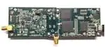
User's Guide
SBAU252 – February 2016
ADS8681EVM-PDK
This user's guide describes the characteristics, operation and use of the ADS8681 evaluation module
(EVM) performance demonstration kit (PDK). This kit is an evaluation platform for the ADS8681 which is a
16-bit, 1-Msps, successive approximation register (SAR) analog-to-digital converter (ADC) featuring
constant resistive input impedance and an enhanced serial multiSPI™ digital interface. This EVM-PDK
eases the evaluation of the ADS8681 device with hardware and software for computer connectivity
through the Universal Serial Bus (USB) interface. This user's guide includes complete circuit descriptions,
schematic diagrams, and a bill of materials (BOM).
The following related documents are available through the Texas Instruments web site at www.ti.com.
Related Documentation
Device
Literature Number
ADS8681
SBAS633
OPA320
SBOS513
REF5040
SBOS410
TPS7A4901
SBVS121
multiSPI is a trademark of Texas Instruments.
Microsoft, Windows are registered trademarks of Microsoft Corporation.
SPI is a trademark of Motorola Mobility LLC.
All other trademarks are the property of their respective owners.
SBAU252 – February 2016
Submit Documentation Feedback
ADS8681EVM-PDK
Copyright © 2016, Texas Instruments Incorporated
1
�www.ti.com
1
2
3
4
5
6
7
8
9
Contents
Overview ...................................................................................................................... 3
1.1
ADS8681EVM-PDK Features ..................................................................................... 3
1.2
ADS8681EVM Features ........................................................................................... 4
EVM Analog Interface ....................................................................................................... 4
2.1
ADC Analog Input Signal Path .................................................................................... 4
2.2
On-Board ADC Reference ......................................................................................... 6
Digital Interfaces ............................................................................................................. 6
3.1
multiSPI® SPI for ADC Digital IO ................................................................................. 6
Power Supplies .............................................................................................................. 7
ADS8681EVM-PDK Initial Setup .......................................................................................... 7
5.1
Default Jumper and Switch Settings ............................................................................. 7
5.2
EVM Graphical User Interface (GUI) Software Installation .................................................... 8
ADS8681EVM-PDK Operation ........................................................................................... 11
6.1
EVM GUI Global Settings for ADC control ..................................................................... 12
6.2
Register Map Configuration Tool ................................................................................ 13
6.3
Time Domain Display Tool ....................................................................................... 14
6.4
Histogram Tool .................................................................................................... 15
6.5
Spectral Analysis Tool ............................................................................................ 16
6.6
Linearity Analysis Tool ............................................................................................ 17
Bill of Materials, PCB Layout, Schematics .............................................................................. 18
7.1
Bill of Materials .................................................................................................... 18
PCB Layout ................................................................................................................. 20
ADS8681EVM-PDK Schematics ......................................................................................... 22
List of Figures
System Connection for Evaluation
2
Schematic of Input Signal Path ............................................................................................ 4
3
Connectors and Jumpers for Input ........................................................................................ 5
4
On-Board Reference Signal Path .......................................................................................... 6
5
Default Settings for Jumper and Switch
6
7
8
9
10
11
12
13
14
15
16
17
18
19
20
21
22
2
........................................................................................
1
3
.................................................................................. 7
EVM GUI Installer may Trigger Antivirus Software ...................................................................... 8
ADS8681 Software Installation Prompts .................................................................................. 9
ADS8681 EVM GUI Folder Post-Installation ........................................................................... 10
EVM-PDK Hardware Setup and LED Indicators ....................................................................... 11
Launch ADS8681 EVM GUI Software ................................................................................... 11
EVM GUI Global Input Parameters ...................................................................................... 12
Register Map Configuration ............................................................................................... 13
Time Domain Display Tool ................................................................................................ 14
Histogram Analysis Tool................................................................................................... 15
Spectral Analysis Tool .................................................................................................... 16
Linearity Analysis Tool .................................................................................................... 17
ADS8681EVM PCB Layer 1 – Top Layer ............................................................................... 20
ADS8681EVM PCB Layer 2 – GND Plane ............................................................................. 20
ADS8681EVM PCB Layer 3 – Power Planes .......................................................................... 21
ADS8681EVM PCB Layer 4 – Bottom Layer .......................................................................... 21
Schematic Diagram of ADS8681EVM – Page 1 ....................................................................... 22
Schematic Diagram of ADS8681EVM – Page 2 ....................................................................... 23
ADS8681EVM-PDK
SBAU252 – February 2016
Submit Documentation Feedback
Copyright © 2016, Texas Instruments Incorporated
�Overview
www.ti.com
1
Overview
The ADS8681EVM-PDK is a platform for evaluating the performance of the ADS8681 Successive
Approximation Register Analog-to-Digital Converter (SAR ADC). The evaluation kit includes the
ADS8681EVM board, the Precision Host Interface (PHI) controller board and accompanying computer
software that enables the user to (1) communicate with the ADC over Universal Serial Bus (USB), (2)
capture data, and (3) perform data analysis.
The ADS8681EVM board includes the ADS8681 SAR ADC, all the peripheral circuits and components
necessary to extract good performance from the ADC.
The PHI board primarily serves three functions:
• Provides a communication interface from the EVM to the computer through a USB port
• Provides the digital input and output signals necessary to communicate with the ADS8681EVM
• Supplies power to all active circuitry on the ADS8681EVM board
Along with the ADS8681EVM and PHI controller boards, this evaluation kit includes an A-to-micro-B USB
cable to connect to a computer.
1.1
ADS8681EVM-PDK Features
The ADS8681EVM-PDK includes the following features:
• Hardware and software required for diagnostic testing as well as accurate performance evaluation of
the ADS8681 ADC
• USB powered - no external power supply is required
• The PHI controller that provides a convenient communication interface to the ADS8681 ADC over a
USB 2.0 (or higher) for power delivery as well as digital input and output
• Easy-to-use evaluation software for Microsoft® Windows® 7, Windows 8, 64-bit operating systems
• The software suite includes graphical tools for data capture, histogram analysis, spectral analysis, and
linearity analysis. It also has a provision for exporting data to a text file for post-processing
Figure 1 illustrates and example system setup for evaluation.
ADS8681EVM
PHI Board
A-to-Micro-B USB
Cable
ADS8681
EVM GUI
Signal
Source
Included in EVM-PDK Kit
Figure 1. System Connection for Evaluation
SBAU252 – February 2016
Submit Documentation Feedback
ADS8681EVM-PDK
Copyright © 2016, Texas Instruments Incorporated
3
�Overview
1.2
www.ti.com
ADS8681EVM Features
The ADS8681EVM includes the following features:
• Integrated 4.096-V precision voltage reference and an option for on-board voltage reference
• Bipolar (±3 × Vref, ±2.5 × Vref, ±1.5 × Vref, ±1.25 × Vref, and ±0.625 × Vref) or unipolar (0 V to 3 ×
Vref, 0 V to 2.5 × Vref, 0 V to 1.5 × Vref, and 0 V to 1.25 × Vref) input ranges
• External signal source by SMA connector
• Jumper-selectable 100-mV and 4-V test signal using on-board buffered DC voltage source
• On-board ultra-low noise low-dropout (LDO) regulator for excellent 5-V single-supply regulation of all
analog circuits
• Options to use external analog and digital power supplies
• Serial interface header for easy connection to PHI controller
2
EVM Analog Interface
The ADS8681 features integrated analog front-end circuitry with constant resistive input impedance
relieving the requirement of external buffer amplifier circuit. The ADS8681EVM is designed for easy
interfacing with analog sources. This section covers the details of the front-end circuit including jumper
configuration for different input test signals and board connectors for a single-ended signal source.
2.1
ADC Analog Input Signal Path
The ADS8681EVM is designed for easy interfacing to analog sources via SMA connector. J1 on
ADS8681EVM is an SMA connector that allows analog source connectivity to the input signal path of the
ADS8681 through a coaxial cable. The schematic for the analog input signal path is shown in Figure 2.
R5 0
ADS8681
VIN AC
R3
(DNP)
D1
(DNP)
R1 0
AIN_P
C1
330 pF
AIN_GND
R4 0
R2 0
"DNP" => Do Not Populate
Figure 2. Schematic of Input Signal Path
When evaluating the ADS8681 performance on the EVM board, the proper resisters can be used to
compose a low-pass filter with a 330-pF capacitor (C0G type) together on the input path.
The internal overvoltage protection circuit of the ADS8681 withstands up to ±20 V on the analog input pin,
however, an external protection circuitry is utilized to provide an additional overvoltage protection with a
transient voltage suppressor (TVS) D1 and a high-power resistor (MMA0204 footprint) R3 on the input
signal path of the ADS8681 on this EVM board.
4
ADS8681EVM-PDK
SBAU252 – February 2016
Submit Documentation Feedback
Copyright © 2016, Texas Instruments Incorporated
�EVM Analog Interface
www.ti.com
The ADC positive input is also accessible through pin 8 of J5. The odd-numbered pins of J5 (J5.Pin1
through J5.Pin7) are shorted together on the board and must be jumpered to any one of the even
numbered pins which are marked as “GND” (J5.Pin2), or “VTH” (J5.Pin4), or “VTL” (J5.Pin6), depending
on which one of the on-board voltage signal sources is used to drive the ADC input as shown in Figure 3.
Figure 3. Connectors and Jumpers for Input
J5.Pin4 and J5.Pin6 on the EVM board are the outputs of the on-board buffered DC voltage sources and
have nominal values of about 4-V and 100-mV, respectively. These are useful for debugging any potential
problems with the front-end circuit or the ADC. The jumper settings on J5 for VTL and VTH on-board
voltage signal and external input signal on J1 are summarized in Table 1.
Table 1. Jumper Settings on J5 for Input
Input
Value
J5.Pin1 < > J5.Pin2 J5.Pin3 < > J5.Pin4 J5.Pin5 < > J5.Pin6 J5.Pin7 < > J5.Pin8
VTL
100 mV
Open
Open
Close
Close
VTH
4V
Open
Close
Open
Close
GND
Ground
Close
Open
Open
Close
Open
Open
Open
Open
External Signal on J1
NOTE: In default operation on EVM board, the input from the external source is connected on J1,
therefore, remove all jumpers on J5 and keep them in open status; refer to Table 1.
SBAU252 – February 2016
Submit Documentation Feedback
ADS8681EVM-PDK
Copyright © 2016, Texas Instruments Incorporated
5
�EVM Analog Interface
2.2
www.ti.com
On-Board ADC Reference
The ADS8681 incorporates a high precision 4.096-V internal voltage reference. Alternatively, the onboard
external 4.096-V precision voltage reference, REF5040 (U2), is selectable for evaluation purposes if the
external voltage reference is necessary for an application system. The reference voltage source is
determined by bit 6 of the ADS8681’s RANGE_SEL_REG register. Configure the reference settings on the
ADS8681EVM-PDK by navigating to the Register Map Config page on the GUI as described in
Section 6.2. By default, the internal reference is enabled after the ADC is powered up, so the jumper on
J3 must not be connected when powering up. If the ADS8681 must be configured with the external
reference, make sure to disable the internal voltage reference by setting bit 6 of the RANGE_SEL_REG
register before using a jumper on J3 to connect the external reference. The schematic for the reference
path is shown in Figure 4.
REF5040
AVDD
2
3
VIN
TEMP
VOUT
TRIM/NR
GND
1 µF
ADS8681
6
5
REFIO
4
1 µF
0.22
J3
0.47
REFGND
10 µF
10 µF
Figure 4. On-Board Reference Signal Path
3
Digital Interfaces
As noted in Section 1, the EVM interfaces with the PHI controller board which, in turn, communicates with
the computer over USB. There are exactly two devices on the EVM with which the PHI communicates –
the ADC (over SPI™, U1) and the EEPROM (over I2C, U5). The EEPROM comes pre-programmed with
the information required to configure and initialize the ADS8681EVM-PDK platform. Once the hardware on
the EVM board has been initialized, the EEPROM is no longer used and is disabled on the EVM board
(refer to Section 5.1.)
3.1
multiSPI® SPI for ADC Digital IO
The ADS8681EVM-PDK supports all the interface modes as detailed in the ADS8681 data sheet
(SBAS633). In addition to the standard SPI modes (with single-, dual-, and quad-SDO lanes) the multiSPI
modes support single- and dual-data output rates and the four possible clock source settings as well. The
PHI is capable of operating at a 1.8-V logic level and is directly connected to the digital I/O lines of the
ADC.
The ADS8681EVM offers 49.9-Ω resistors between the SPI signals and J2 to aid with signal integrity.
Typically, in high-speed SPI communication, fast signal edges can cause overshoot; these 49.9-Ω
resistors slow down the signal edges in order to minimize signal overshoot.
6
ADS8681EVM-PDK
SBAU252 – February 2016
Submit Documentation Feedback
Copyright © 2016, Texas Instruments Incorporated
�Power Supplies
www.ti.com
4
Power Supplies
The PHI provides multiple power supply options for the ADS8681EVM, derived from the computer’s USB
supply. The EEPROM on the ADS8681EVM uses a common 3.3-V power supply (EVM_ID_PWR)
generated directly by the PHI. The ADC and analog input drive circuits are powered by the TPS7A4901
on-board the EVM. The TPS7A4901 is a low-noise linear regulator that uses the 5.5-V supply out of a
switching regulator on the PHI to generate a much cleaner 5-V output (AVDD) for all analog circuits on the
EVM board. This analog supply can be also provided by an external power supply when a jumper is
installed on pin 2-3 position of J4.The 3.3-V power supply to the digital section of the ADC is provided
directly by an LDO on the PHI (EVM_DVDD).
The power supply for each active component on the EVM is bypassed with a ceramic capacitor placed
close to that component. Additionally, the EVM layout utilizes thick traces or large copper fill areas, where
possible, between bypass capacitors and their loads to minimize inductance along the load current path,
refer to the schematics in Section 7 for more details.
5
ADS8681EVM-PDK Initial Setup
This section explains the initial hardware and software setup procedure that must be completed for
properly operating the ADS8681EVM-PDK.
5.1
Default Jumper and Switch Settings
Upon unpacking, the EVM should already be configured with the default jumper settings (Figure 5).
Close
Top
Figure 5. Default Settings for Jumper and Switch
The default setting includes no jumpers installed on J5 making J1 the input signal source. The default
position of J4 is position 1 so that the linear regulator is powering the system using 5.5 V from the PHI
controller. Place switch S1 at position 1-2 (to the top) enabling EEPROM write protection. Leave J3 open
so the ADC’s internal voltage reference is used when powering up. J6 is open to disconnect ALARM
output connection to the PHI controller. The locations for the default jumpers and switch are shown in
Figure 5.
SBAU252 – February 2016
Submit Documentation Feedback
ADS8681EVM-PDK
Copyright © 2016, Texas Instruments Incorporated
7
�ADS8681EVM-PDK Initial Setup
5.2
www.ti.com
EVM Graphical User Interface (GUI) Software Installation
NOTE: Manually disable any antivirus software running on the computer before connecting the SD
card or downloading the EVM GUI installer onto the local hard disk. Otherwise, depending on
antivirus settings, an error message such as the one shown in Figure 6 may appear, or the
installer .exe file may be deleted.
Figure 6. EVM GUI Installer may Trigger Antivirus Software
Download the latest version of the installer from the Tools and Software folder of the ADS8681 and run
the GUI installer. Accept the license agreements and follow the on-screen instructions to complete the
installation as shown in Figure 7.
As a part of the ADS8681 EVM GUI installation, a prompt with a Device Driver Installation will appear on
the screen also shown in Figure 7.
8
ADS8681EVM-PDK
SBAU252 – February 2016
Submit Documentation Feedback
Copyright © 2016, Texas Instruments Incorporated
�ADS8681EVM-PDK Initial Setup
www.ti.com
Figure 7. ADS8681 Software Installation Prompts
SBAU252 – February 2016
Submit Documentation Feedback
ADS8681EVM-PDK
Copyright © 2016, Texas Instruments Incorporated
9
�ADS8681EVM-PDK Initial Setup
www.ti.com
NOTE: A notice may appear on the screen stating that Windows cannot verify the publisher of this
driver software; Select ‘Install this driver software anyway’.
After these installations, verify that “C:\Program Files (x86)\Texas Instruments\ADS8681 EVM” installation
path is shown in Figure 8.
Figure 8. ADS8681 EVM GUI Folder Post-Installation
10
ADS8681EVM-PDK
SBAU252 – February 2016
Submit Documentation Feedback
Copyright © 2016, Texas Instruments Incorporated
�ADS8681EVM-PDK Operation
www.ti.com
6
ADS8681EVM-PDK Operation
The following instructions are a step-by-step guide for connecting the ADS9110EVM-PDK to the computer
and evaluating the performance of the ADS8681:
1. Connect the ADS8681EVM to the PHI. Install the two screws as indicated in Figure 9.
2. Use the provided USB cable to connect the PHI to the computer
• LED D5 on the PHI lights up indicating that the PHI has powered up
• LEDs D1 and D2 on the PHI start blinking, indicating the PHI is booted up and communicating with
the EVM
Figure 9. EVM-PDK Hardware Setup and LED Indicators
3. Launch the ADS8681EVM GUI software from the Start Menu of computer, Desktop Shortcut, or
Installation folder (Figure 10).
Figure 10. Launch ADS8681 EVM GUI Software
SBAU252 – February 2016
Submit Documentation Feedback
ADS8681EVM-PDK
Copyright © 2016, Texas Instruments Incorporated
11
�ADS8681EVM-PDK Operation
6.1
www.ti.com
EVM GUI Global Settings for ADC control
Although the EVM GUI does not allow direct access to the levels and timing configuration of the ADC
digital interface, the EVM GUI does give users high-level control over virtually all functions of the
ADS8681, including interface modes, sampling rate, and number of samples captured.
The various functions of the ADS8681 are exercised through the input parameters of the GUI (as well as
their default values), as illustrated in Figure 11. These are global settings because they persist across the
GUI tools listed in the top left pane as Pages, which include Register Map Configuration, Time Domain
Display, Spectral Analysis, Histogram Analysis, and Linearity Analysis tools.
4. Information Area
3. GUI
Function
Select
1. Host
Configuration
2. Clock
and
Sampling
Rate
Figure 11. EVM GUI Global Input Parameters
The host configuration options in this pane allow the choice of various SPI and multiSPI host interface
options available on the ADS8681. The host always communicates with the ADS8681 using the standard
SPI protocol over the single SDI lane, irrespective of the mode selected for Data Capture.
The drop-down boxes under the Device Modes sub-menu allows selection of the data capture mode. The
Bus Width drop-down allows selection between Single-, and Dual-SDO lanes; Data Read between Source
and System Synchronous modes; Device Range between Bipolar and Unipolar modes, and Voltage
Range between 3 × Vref, 2.5 × Vref, 1.5 × Vref, 1.25 × Vref, and 0.625 × Vref options. Detailed
descriptions of each of these modes are available in the ADS8681 datasheet (SBAS633).
Selection of SCLK Frequency and Sampling Rate is allowed on this pane and is dependent of the Device
Modes selected. Select or specify a target SCLK frequency (in Hz) and the GUI tries to match this as
closely as possible by changing the PHI PLL settings and the achievable frequency that may differ from
the target value displayed. Similarly, the sampling rate of the ADC can be adjusted by modifying the
Target Sampling Rate argument (also in Hz). The achievable ADC sampling rate may differ from the target
value, depending on the applied SCLK frequency and selected Device Mode and the closest match
achievable is displayed. This pane allows the choice of various settings available on the ADS8681 in an
iterative fashion until the best settings for the corresponding test scenario are discovered.
12
ADS8681EVM-PDK
SBAU252 – February 2016
Submit Documentation Feedback
Copyright © 2016, Texas Instruments Incorporated
�ADS8681EVM-PDK Operation
www.ti.com
The final option in this pane is the selection for the Update Mode. The default value is “Immediate” which
indicates that the interface settings selection is applied to configure both the host and the ADS8681
instantly. The Manual option indicates that the selection is made only when the final choices are decided
upon and the user is ready to configure the device. This is described in more detail in the following
section.
The GUI is switched between hardware mode and simulation mode by checking and unchecking the
Connected to Hardware box in the top right area at any time.
6.2
Register Map Configuration Tool
The register map configuration tool allows viewing and modification all of the registers of the ADS8681.
This is selected by clicking on the Register Map Config radio button at the Pages section of the left pane
as indicated in Figure 12.
Figure 12. Register Map Configuration
On power up and initialization, the values on this page correspond to the reset values of the device
registers. The register values are changed by single-clicking the corresponding bit field of the registers. If
interface mode settings are affected by the change in register values, this change reflects on the left pane
immediately. The impact of changes in the register value reflects on the ADS8681 device on the
ADS8681EVM-PDK based on the Update Mode selection as described in Section 6.1.
SBAU252 – February 2016
Submit Documentation Feedback
ADS8681EVM-PDK
Copyright © 2016, Texas Instruments Incorporated
13
�ADS8681EVM-PDK Operation
6.3
www.ti.com
Time Domain Display Tool
The Time Domain Display tool allows visualization of the ADS8681's response to a given input signal. This
tool is useful for both studying the behavior and debugging any problems with the ADC or drive circuits.
The user can trigger a capture of the data of the selected number of samples from the ADS8681, as per
the current interface mode settings using the capture button as indicated on Figure 13. The sample
indices are on the X-axis and there are two Y-axes showing the corresponding output codes as well as the
equivalent analog voltages based on the specified reference voltage, the selected Device Range and
Voltage Range. The measured maximum and minimum code and equivalent voltage are also shown in the
bottom right pane.
Figure 13. Time Domain Display Tool
14
ADS8681EVM-PDK
SBAU252 – February 2016
Submit Documentation Feedback
Copyright © 2016, Texas Instruments Incorporated
�ADS8681EVM-PDK Operation
www.ti.com
6.4
Histogram Tool
Noise degrades ADC resolution and the histogram tool is used to estimate Effective Resolution, which is
an indicator of the number of bits of ADC resolution lost due to noise generated by the various sources
connected to the ADC when measuring a DC signal. The cumulative effect of noise coupling to the ADC
output from sources such as the input drive circuits, the reference drive circuit, the ADC power supply, and
the ADC itself is reflected in the standard deviation of the ADC’s output code histogram, obtained by
performing multiple conversions of a DC input applied to a given channel.
The histogram analysis corresponding to a DC input is displayed by selecting Histogram Analysis on
Pages and clicking on the Capture button as shown in Figure 14. The Analysis results include Mean,
Sigma, Min Code, Max Code, and Code spread.
The X Scale of Histogram Analysis results are changed by selecting Auto mode or the default Fit to code
range in the top right area, which is similar as the Y scale fit in the Time Domain Display tool.
Figure 14. Histogram Analysis Tool
SBAU252 – February 2016
Submit Documentation Feedback
ADS8681EVM-PDK
Copyright © 2016, Texas Instruments Incorporated
15
�ADS8681EVM-PDK Operation
6.5
www.ti.com
Spectral Analysis Tool
The spectral analysis tool is intended to evaluate the dynamic performance (SNR, THD, SFDR, SINAD,
and ENOB) of the ADS9110 SAR ADC through single-tone sinusoidal signal FFT analysis using the 7term Blackman-Harris window setting.
The spectral analysis corresponding to a 1-kHz sinusoidal signal and 1-Msps sampling rate is displayed
on clicking the Capture button as shown in Figure 15.
The expected ADC input is a sinusoidal signal of peak-to-peak amplitude close to the ADC’s full-scale
input range (FSR). The RMS power of the input signal normalized to FSR is shown in the Signal Power
(dBFS) field and is about –0.5 dBFS (or about 95% × FSR) to avoid the input clipping.
The sampling rate of the ADC is adjusted by modifying the target sampling rate (sps) argument which is a
global setting (it affects all tools). The achievable ADC sampling rate may differ from the target value
depending on the applied SCLK frequency and PHI PLL settings. Note that the user is also required to
specify a target SCLK frequency which the tool tries to match as exactly as possible by iteratively
changing the PHI PLL settings until convergence.
Figure 15. Spectral Analysis Tool
Finally, the FFT tool includes windowing options that are required to mitigate the effects of non-coherent
sampling (this discussion is beyond the scope of this document). The 7-Term Blackman Harris window is
the default option and has sufficient dynamic range to resolve the frequency components of up to a 24-bit
ADC. Note that the None” option corresponds to not using a window (or using a rectangular window) and
is not recommended.
16
ADS8681EVM-PDK
SBAU252 – February 2016
Submit Documentation Feedback
Copyright © 2016, Texas Instruments Incorporated
�ADS8681EVM-PDK Operation
www.ti.com
6.6
Linearity Analysis Tool
The linearity analysis tool measures and generates the DNL and INL plots over code for the specific
ADS8681 installed in the evaluation board. A 1-kHz sinusoidal input signal with very low distortion is
applied for linearity analysis and shown in Figure 16, which is slightly saturated and ensures there is no
damage to the ADC. It is critical for the external source linearity to be better than the ADC linearity. This is
important to ensure that the measured system performance reflects the linearity errors of the ADC and is
not limited by the performance of the signal source.
Figure 16. Linearity Analysis Tool
SBAU252 – February 2016
Submit Documentation Feedback
ADS8681EVM-PDK
Copyright © 2016, Texas Instruments Incorporated
17
�Bill of Materials, PCB Layout, Schematics
7
www.ti.com
Bill of Materials, PCB Layout, Schematics
This section contains the ADS8681EVM bill of materials, PCB layout, and the EVM schematics.
7.1
Bill of Materials
Table 2 lists the EVM BOM.
Table 2. ADS8681EVM-PDK Bill of Materials
Manufacturer Part Number
QTY
Reference Designator
Manufacturer
Description
1891
4
@H1, @H2, @H3, @H4
Keystone
Hex Standoff, #4-40, Aluminum, 1/4"
MPMS 002 0005 PH
2
@H5, @H6
B&F Fastener Supply
MACHINE SCREW PAN PHILLIPS M2
C1608C0G2A331J
1
C1
TDK
CAP, CERM, 330 pF, 100 V, +/- 5%, C0G/NP0, 0603
C0603C104K5RACTU
3
C2, C10, C14
Kemet
CAP, CERM, 0.1 μF, 50 V, +/- 10%, X7R, 0603
C1608X7R1C105K
9
C3, C4, C5, C6, C7, C11, C13, C15, C19
TDK
CAP, CERM, 1 μF, 16 V, +/- 10%, X7R, 0603
CL21A106KAFN3NE
6
C8, C9, C16, C18, C21, C22
Samsung Electro-Mechanics
CAP, CERM, 10 μF, 25 V, +/- 10%, X5R, 0805
GRM21BR61C226ME44
1
C12
Murata
CAP, CERM, 22 μF, 16 V, +/- 20%, X5R, 0805
C1608C0G1H103J080AA
2
C17, C20
TDK
CAP, 10000pF, 0603, 5%, 50V, C0G
LG M67K-G1J2-24-Z
1
D2
OSRAM
LED, Green, SMD
MMSZ4696T1G
1
D3
ON Semiconductor
Diode, Zener, 9.1 V, 500 mW, SOD-123
PMSSS 440 0025 PH
4
H1, H2, H3, H4
B&F Fastener Supply
MACHINE SCREW PAN PHILLIPS 4-40
9774050243R
2
H5, H6
Wurth Elektronik
ROUND STANDOFF M2 STEEL 5MM
102-1092-BL-00100
1
H7
CNC Tech
CABLE USB A MALE-B MICRO MALE 1M (Kit Item)
901-143
1
J1
Amphenol RF
Connector, TH, Right Angle SMA 50 ohm
QTH-030-01-L-D-A
1
J2
Samtec
Header(Shrouded), 19.7mil, 30x2, Gold, SMT
87898-0204
2
J3, J6
Molex
Header, 2.54 mm, 2x1, Gold, R/A, SMT
TSM-103-01-L-SV
1
J4
Samtec
Header, 100mil, 3x1, Gold, SMT
0015910080
1
J5
Molex
Header, 100mil, 4x2, Gold, SMT
BC847CLT1G
1
Q1
ON Semiconductor
Transistor, NPN, 45 V, 0.1 A, SOT-23
CRCW06030000Z0EA
5
R1, R2, R4, R5, R31
Vishay-Dale
RES, 0, 5%, 0.1 W, 0603
RC0603FR-0710KL
7
R6, R9, R13, R20, R21, R30, R32
Yageo America
RES, 10.0 k, 1%, 0.1 W, 0603
RC0603FR-07249RL
2
R7, R8
Yageo America
RES, 249, 1%, 0.1 W, 0603
RT0603BRD071KL
2
R10, R11
Yageo America
RES, 1.00 k, 0.1%, 0.1 W, 0603
ERJ-3RQFR47V
1
R12
Panasonic
RES, 0.47, 1%, 0.1 W, 0603
CRCW040249R9FKED
8
R14, R17, R19, R23, R26, R27, R28, R29
Vishay-Dale
RES, 49.9, 1%, 0.063 W, 0402
CRCW0402220KJNED
1
R15
Vishay-Dale
RES, 220 k, 5%, 0.063 W, 0402
RG1608P-1023-B-T5
1
R16
Susumu Co Ltd
RES, 102 k, 0.1%, 0.1 W, 0603
CRCW0402100KFKED
1
R18
Vishay-Dale
RES, 100 k, 1%, 0.063 W, 0402
RC0402JR-070RL
1
R22
Yageo America
RES, 0, 5%, 0.063 W, 0402
RG1608P-334-B-T5
1
R24
Susumu Co Ltd
RES, 330 k, 0.1%, 0.1 W, 0603
18
ADS8681EVM-PDK
SBAU252 – February 2016
Submit Documentation Feedback
Copyright © 2016, Texas Instruments Incorporated
�Bill of Materials, PCB Layout, Schematics
www.ti.com
Table 2. ADS8681EVM-PDK Bill of Materials (continued)
Manufacturer Part Number
QTY
Reference Designator
Manufacturer
Description
ERJ-3RQFR22V
2
R25, R34
Panasonic
RES, 0.22, 1%, 0.1 W, 0603
CAS-120TA
1
S1
Copal Electronics
Switch, Slide, SPDT 100mA, SMT
969102-0000-DA
1
SH-J4
3M
Shunt, 100mil, Gold plated, Black
5015
5
TP1, TP2, TP3, TP4, TP5
Keystone
Test Point, Miniature, SMT
ADS8681IPWR
1
U1
Texas Instruments
SAR ADC with 16 Bits, Single Channel, 1Msps, and Bipolar Inputs off +5 V Supply,
PW0016A
REF5040ID
1
U2
Texas Instruments
Low Noise, Very Low Drift, Precision Voltage Reference, -40 to 125 degC, 8-pin SOIC (D),
Green (RoHS & no Sb/Br)
OPA320AIDBVR
1
U3
Texas Instruments
Precision, 20 MHz, 0.9 pA Ib, RRIO, CMOS Operational Amplifier, 1.8 to 5.5 V, -40 to 125
degC, 5-pin SOT23 (DBV0005A), Green (RoHS & no Sb/Br)
TPS7A4901DGNR
1
U4
Texas Instruments
Single Output High PSRR LDO, 150 mA, Adjustable 1.2 to 33 V Output, 3 to 36 V Input,
with Ultra-Low Noise, 8-pin MSOP (DGN), -40 to 125 degC, Green (RoHS & no Sb/Br)
BR24G32FVT-3AGE2
1
U5
Rohm
I2C BUS EEPROM (2-Wire), TSSOP-B8
SBAU252 – February 2016
Submit Documentation Feedback
ADS8681EVM-PDK
Copyright © 2016, Texas Instruments Incorporated
19
�PCB Layout
8
www.ti.com
PCB Layout
Figure 17 through Figure 20 illustrate the EVM PCB layouts.
Figure 17. ADS8681EVM PCB Layer 1 – Top Layer
Figure 18. ADS8681EVM PCB Layer 2 – GND Plane
20
ADS8681EVM-PDK
SBAU252 – February 2016
Submit Documentation Feedback
Copyright © 2016, Texas Instruments Incorporated
�PCB Layout
www.ti.com
Figure 19. ADS8681EVM PCB Layer 3 – Power Planes
Figure 20. ADS8681EVM PCB Layer 4 – Bottom Layer
SBAU252 – February 2016
Submit Documentation Feedback
ADS8681EVM-PDK
Copyright © 2016, Texas Instruments Incorporated
21
�ADS8681EVM-PDK Schematics
9
www.ti.com
ADS8681EVM-PDK Schematics
Figure 21 and Figure 22 illustrate the EVM schematics.
1
2
3
4
5
6
"DNP" => Do Not Populate
A
A
TP1
J1
1
1
3
5
7
GND
2
4
6
8
0
DNP
R3
100
VTH
GND
RVS
DNP D1
VTL
AVDD
DVDD
DVDD
4.5V*sin(2*pi*fin*t)
TP4
C3
1µF
GND
C4
1µF
2
3
VTH
R7
249
C7
1µF
R6
10.0k
B
GND
7
AIN_P
15
ALARM/SDO-1/GPO
14
C1
330pF
R4
0
GND
R2
R17
J2
Q1
DVDD
R18
J6
100k
1
2
AIN_GND
GND
0
GND
R20
10.0k
R21
10.0k
R19
49.9
SDO-1/GPO
SDI
CONVST/CS
R23
49.9
SDO-0
SCLK
GND
C10
0.1uF
3
R34
0.22
4
GND
C11
1µF
GND
J3
U2B
REF5040ID
REFIO
SCLK
6
REFCAP
0.22
C12
22µF
C9
GND
NC
DNC
DNC
R12
0.47
CONVST/CS
C13
1µF
SDI
C8
10µF
7
1
8
TEMP
SDO-0
4
R25
6
5
5
REFGND
RST
GND
10µF
GND
U1
12
R26
49.9
SCLK
11
R27
49.9
CONVST/CS
10
R28
49.9
SDI
R29
49.9
RST
9
DGND
VOUT
TRIM/NR
13
DVDD
R30
HOST_A2_CLK2
HOST_A2_CLK3
HOST_A2_CLK4
ALARM
SDO-0
SDO-1/GPO
EVM_DVDD
RST
10.0k
1
REF5040ID
VIN
AGND
U2A
2
3
AVDD
2
1
GND
ALARM
1
220k
49.9
8
49.9
EVM_RAW_5V
R15
RVS
0
C5
1µF
2
C6
1µF
R1
R10 1.00k
R14
1
Green
DVDD
1
GND
AVDD
4
R8
249
VTL
U3
OPA320AIDBVR
2
GND
GND
R9
10.0k
D2
2
5
0.1uF
R11
1.00k
3
GND
C2 AVDD
16
2
3
4
5
R5
J5
901-143
ADS8681IPWR
GND
EVM_ID_SDA
EVM_ID_SCL
EVM_PRSNT_N
GND
EXT Power Supply
TP2
EVM_REG_5V5
2
4
6
8
10
12
14
16
18
20
22
24
26
28
30
32
34
36
38
40
42
44
46
48
50
52
54
56
58
60
MP1
MP2
(+6~+9V)
2
4
6
8
10
12
14
16
18
20
22
24
26
28
30
32
34
36
38
40
42
44
46
48
50
52
54
56
58
60
GND
GND
1
3
5
7
9
11
13
15
17
19
21
23
25
27
29
31
33
35
37
39
41
43
45
47
49
51
53
55
57
59
GND
GND
1
3
5
7
9
11
13
15
17
19
21
23
25
27
29
31
33
35
37
39
41
43
45
47
49
51
53
55
57
59
GND
B
EVM_ID_PWR
MP3
MP4
R22
C
GND
0
C15
1µF
TP5
EVM_DVDD
GND
EVM_ID_PWR
EVM_ID_PWR
EVM_ID_PWR
C16
10µF
8
5
C19
1µF
EVM_REG_5V5
3
7
IN
OUT
EN
NC
DNC
FB
NR/SS
GND
3
C18
10µF
6
4
9
GND
EVM_REG_5V5 EVM_ID_PWR
4
A0
VCC
A1
WP
A2
SCL
VSS
SDA
8
1
0.1uF
7
WP
6
EVM_ID_SCL
5
EVM_ID_SDA
GND
BR24G32FVT-3AGE2
EP GND
GND
2
R24
330k
C17
10000pF
R13
10.0k
U5
AVDD
1
2
C14
R32
10.0k
1
U4 TPS7A4901DGNR
3
2
1
C
GND
DVDD
R31
0
GND
J4
QTH-030-01-L-D-A
TP3
D3
C20
R16
10000pF 102k
GND
GND
GND
C21
10µF
C22
10µF
GND
2
S1
3
GND
GND
GND
D
D
Orderable:
ADS8681EVM-PDK
TID #:
N/A
Number: PA017
Rev: A
Texas Instruments and/or its licensors do not warra
nt the accuracy or completeness of this specificati
on or any information contained therein. Texas ruments
Inst
and/or its licensors do not SVN Rev: Version control disabled
warrant that this design will meet the specificatio
ns, will be suitable for your application or rfitany
fo particular purpose, or will operate in anlementation.
imp
Texas Instruments and/or its Drawn By:Dale Li
licensors do not warrant that the design is product
ion worthy. You should completely validate and test
your design implementation to confirm the system
unctionality
f
for your application. Engineer: Dale Li
1
2
3
4
5
Designed for:Public Release
Project Title:ADS8681EVM-PDK
Sheet Title:
Assembly Variant:001
File: PA017A_Schematic.SchDoc
Contact: http://www.ti.com/support
Mod. Date: 2/12/2016
Sheet: 1 of 2
Size: B
http://www.ti.com
© Texas Instruments2015
6
Figure 21. Schematic Diagram of ADS8681EVM – Page 1
22
ADS8681EVM-PDK
SBAU252 – February 2016
Submit Documentation Feedback
Copyright © 2016, Texas Instruments Incorporated
�ADS8681EVM-PDK Schematics
www.ti.com
1
2
A
3
Logo2
Logo3
PCB
LOGO
PCB
LOGO
PCB
LOGO
Texas Instruments
Pb-Free Symbol
FCC disclaimer
@H6
MPMS 002 0005 PH
MPMS 002 0005 PH
H5
H6
9774050243R
9774050243R
5
6
A
Logo1
@H5
4
H7
MECH
102-1092-BL-00100
CABLE USB A MALE-B MICRO MALE 1M (Kit Item)
PCB Number: PA017
PCB Rev: A
Printed Circuit Board
B
B
H1
H2
H3
H4
PCB: Used in BOM report
PMSSS 440 0025 PH PMSSS 440 0025 PH PMSSS 440 0025 PH PMSSS 440 0025 PH
@H1
@H2
@H3
@H4
1891
1891
1891
1891
Update Description to match PCB's description
ZZ1
Assembly Note
These assemblies are ESD sensitive, ESD precautions
shall be observed.
SH-J4
ZZ2
Assembly Note
These assemblies must be clean and free from flux
nd all
a contaminants. Use of no clean flux is not
ceptable.
ac
C
FID1
FID2
FID3
FID4
FID5
ZZ3
Assembly Note
These assemblies must comply with workmanship stand
ards IPC-A-610 Class 2, unless otherwise specified.
FID6
C
ZZ4
Assembly Note
Place @H5 and @H6 screws in H5 and H6 standoffs
ZZ5
Assembly Note
Place H1, H2, H3, H4 screws in @H1, @H2, @H3, @H4
tandoffs
s
Label Table
Variant
001
Label Text
ADS8681EVM-PDK
ZZ6
Assembly Note
Mount Shut at: J4: 1-2pins
D
D
Orderable: ADS8681EVM-PDK
TID #:
N/A
Number: PA017
Rev: A
Texas Instruments and/or its licensors do not warra
nt the accuracy or completeness of this specificati
on or any information contained therein. Texas ruments
Inst
and/or its licensors do not SVN Rev: Version control disabled
warrant that this design will meet the specificatio
ns, will be suitable for your application or rfitany
fo particular purpose, or will operate in anlementation.
imp
Texas Instruments and/or its Drawn By:Dale Li
licensors do not warrant that the design is product
ion worthy. You should completely validate and test
your design implementation to confirm the system
unctionality
f
for your application. Engineer: Dale Li
1
2
3
4
5
Designed for:Public Release
Project Title:ADS8681EVM-PDK
Sheet Title:
Assembly Variant:001
File: PA017A_Hardware.SchDoc
Contact: http://www.ti.com/support
Mod. Date: 1/4/2016
Sheet: 2 of 2
Size: B
http://www.ti.com
© Texas Instruments2015
6
Figure 22. Schematic Diagram of ADS8681EVM – Page 2
SBAU252 – February 2016
Submit Documentation Feedback
ADS8681EVM-PDK
Copyright © 2016, Texas Instruments Incorporated
23
�STANDARD TERMS AND CONDITIONS FOR EVALUATION MODULES
1.
Delivery: TI delivers TI evaluation boards, kits, or modules, including any accompanying demonstration software, components, or
documentation (collectively, an “EVM” or “EVMs”) to the User (“User”) in accordance with the terms and conditions set forth herein.
Acceptance of the EVM is expressly subject to the following terms and conditions.
1.1 EVMs are intended solely for product or software developers for use in a research and development setting to facilitate feasibility
evaluation, experimentation, or scientific analysis of TI semiconductors products. EVMs have no direct function and are not
finished products. EVMs shall not be directly or indirectly assembled as a part or subassembly in any finished product. For
clarification, any software or software tools provided with the EVM (“Software”) shall not be subject to the terms and conditions
set forth herein but rather shall be subject to the applicable terms and conditions that accompany such Software
1.2 EVMs are not intended for consumer or household use. EVMs may not be sold, sublicensed, leased, rented, loaned, assigned,
or otherwise distributed for commercial purposes by Users, in whole or in part, or used in any finished product or production
system.
2
Limited Warranty and Related Remedies/Disclaimers:
2.1 These terms and conditions do not apply to Software. The warranty, if any, for Software is covered in the applicable Software
License Agreement.
2.2 TI warrants that the TI EVM will conform to TI's published specifications for ninety (90) days after the date TI delivers such EVM
to User. Notwithstanding the foregoing, TI shall not be liable for any defects that are caused by neglect, misuse or mistreatment
by an entity other than TI, including improper installation or testing, or for any EVMs that have been altered or modified in any
way by an entity other than TI. Moreover, TI shall not be liable for any defects that result from User's design, specifications or
instructions for such EVMs. Testing and other quality control techniques are used to the extent TI deems necessary or as
mandated by government requirements. TI does not test all parameters of each EVM.
2.3 If any EVM fails to conform to the warranty set forth above, TI's sole liability shall be at its option to repair or replace such EVM,
or credit User's account for such EVM. TI's liability under this warranty shall be limited to EVMs that are returned during the
warranty period to the address designated by TI and that are determined by TI not to conform to such warranty. If TI elects to
repair or replace such EVM, TI shall have a reasonable time to repair such EVM or provide replacements. Repaired EVMs shall
be warranted for the remainder of the original warranty period. Replaced EVMs shall be warranted for a new full ninety (90) day
warranty period.
3
Regulatory Notices:
3.1 United States
3.1.1
Notice applicable to EVMs not FCC-Approved:
This kit is designed to allow product developers to evaluate electronic components, circuitry, or software associated with the kit
to determine whether to incorporate such items in a finished product and software developers to write software applications for
use with the end product. This kit is not a finished product and when assembled may not be resold or otherwise marketed unless
all required FCC equipment authorizations are first obtained. Operation is subject to the condition that this product not cause
harmful interference to licensed radio stations and that this product accept harmful interference. Unless the assembled kit is
designed to operate under part 15, part 18 or part 95 of this chapter, the operator of the kit must operate under the authority of
an FCC license holder or must secure an experimental authorization under part 5 of this chapter.
3.1.2
For EVMs annotated as FCC – FEDERAL COMMUNICATIONS COMMISSION Part 15 Compliant:
CAUTION
This device complies with part 15 of the FCC Rules. Operation is subject to the following two conditions: (1) This device may not
cause harmful interference, and (2) this device must accept any interference received, including interference that may cause
undesired operation.
Changes or modifications not expressly approved by the party responsible for compliance could void the user's authority to
operate the equipment.
FCC Interference Statement for Class A EVM devices
NOTE: This equipment has been tested and found to comply with the limits for a Class A digital device, pursuant to part 15 of
the FCC Rules. These limits are designed to provide reasonable protection against harmful interference when the equipment is
operated in a commercial environment. This equipment generates, uses, and can radiate radio frequency energy and, if not
installed and used in accordance with the instruction manual, may cause harmful interference to radio communications.
Operation of this equipment in a residential area is likely to cause harmful interference in which case the user will be required to
correct the interference at his own expense.
SPACER
SPACER
SPACER
SPACER
SPACER
SPACER
SPACER
SPACER
�FCC Interference Statement for Class B EVM devices
NOTE: This equipment has been tested and found to comply with the limits for a Class B digital device, pursuant to part 15 of
the FCC Rules. These limits are designed to provide reasonable protection against harmful interference in a residential
installation. This equipment generates, uses and can radiate radio frequency energy and, if not installed and used in accordance
with the instructions, may cause harmful interference to radio communications. However, there is no guarantee that interference
will not occur in a particular installation. If this equipment does cause harmful interference to radio or television reception, which
can be determined by turning the equipment off and on, the user is encouraged to try to correct the interference by one or more
of the following measures:
•
•
•
•
Reorient or relocate the receiving antenna.
Increase the separation between the equipment and receiver.
Connect the equipment into an outlet on a circuit different from that to which the receiver is connected.
Consult the dealer or an experienced radio/TV technician for help.
3.2 Canada
3.2.1
For EVMs issued with an Industry Canada Certificate of Conformance to RSS-210
Concerning EVMs Including Radio Transmitters:
This device complies with Industry Canada license-exempt RSS standard(s). Operation is subject to the following two conditions:
(1) this device may not cause interference, and (2) this device must accept any interference, including interference that may
cause undesired operation of the device.
Concernant les EVMs avec appareils radio:
Le présent appareil est conforme aux CNR d'Industrie Canada applicables aux appareils radio exempts de licence. L'exploitation
est autorisée aux deux conditions suivantes: (1) l'appareil ne doit pas produire de brouillage, et (2) l'utilisateur de l'appareil doit
accepter tout brouillage radioélectrique subi, même si le brouillage est susceptible d'en compromettre le fonctionnement.
Concerning EVMs Including Detachable Antennas:
Under Industry Canada regulations, this radio transmitter may only operate using an antenna of a type and maximum (or lesser)
gain approved for the transmitter by Industry Canada. To reduce potential radio interference to other users, the antenna type
and its gain should be so chosen that the equivalent isotropically radiated power (e.i.r.p.) is not more than that necessary for
successful communication. This radio transmitter has been approved by Industry Canada to operate with the antenna types
listed in the user guide with the maximum permissible gain and required antenna impedance for each antenna type indicated.
Antenna types not included in this list, having a gain greater than the maximum gain indicated for that type, are strictly prohibited
for use with this device.
Concernant les EVMs avec antennes détachables
Conformément à la réglementation d'Industrie Canada, le présent émetteur radio peut fonctionner avec une antenne d'un type et
d'un gain maximal (ou inférieur) approuvé pour l'émetteur par Industrie Canada. Dans le but de réduire les risques de brouillage
radioélectrique à l'intention des autres utilisateurs, il faut choisir le type d'antenne et son gain de sorte que la puissance isotrope
rayonnée équivalente (p.i.r.e.) ne dépasse pas l'intensité nécessaire à l'établissement d'une communication satisfaisante. Le
présent émetteur radio a été approuvé par Industrie Canada pour fonctionner avec les types d'antenne énumérés dans le
manuel d’usage et ayant un gain admissible maximal et l'impédance requise pour chaque type d'antenne. Les types d'antenne
non inclus dans cette liste, ou dont le gain est supérieur au gain maximal indiqué, sont strictement interdits pour l'exploitation de
l'émetteur
3.3 Japan
3.3.1
Notice for EVMs delivered in Japan: Please see http://www.tij.co.jp/lsds/ti_ja/general/eStore/notice_01.page 日本国内に
輸入される評価用キット、ボードについては、次のところをご覧ください。
http://www.tij.co.jp/lsds/ti_ja/general/eStore/notice_01.page
3.3.2
Notice for Users of EVMs Considered “Radio Frequency Products” in Japan: EVMs entering Japan may not be certified
by TI as conforming to Technical Regulations of Radio Law of Japan.
If User uses EVMs in Japan, not certified to Technical Regulations of Radio Law of Japan, User is required by Radio Law of
Japan to follow the instructions below with respect to EVMs:
1.
2.
3.
Use EVMs in a shielded room or any other test facility as defined in the notification #173 issued by Ministry of Internal
Affairs and Communications on March 28, 2006, based on Sub-section 1.1 of Article 6 of the Ministry’s Rule for
Enforcement of Radio Law of Japan,
Use EVMs only after User obtains the license of Test Radio Station as provided in Radio Law of Japan with respect to
EVMs, or
Use of EVMs only after User obtains the Technical Regulations Conformity Certification as provided in Radio Law of Japan
with respect to EVMs. Also, do not transfer EVMs, unless User gives the same notice above to the transferee. Please note
that if User does not follow the instructions above, User will be subject to penalties of Radio Law of Japan.
SPACER
SPACER
SPACER
SPACER
SPACER
�【無線電波を送信する製品の開発キットをお使いになる際の注意事項】 開発キットの中には技術基準適合証明を受けて
いないものがあります。 技術適合証明を受けていないもののご使用に際しては、電波法遵守のため、以下のいずれかの
措置を取っていただく必要がありますのでご注意ください。
1.
2.
3.
電波法施行規則第6条第1項第1号に基づく平成18年3月28日総務省告示第173号で定められた電波暗室等の試験設備でご使用
いただく。
実験局の免許を取得後ご使用いただく。
技術基準適合証明を取得後ご使用いただく。
なお、本製品は、上記の「ご使用にあたっての注意」を譲渡先、移転先に通知しない限り、譲渡、移転できないものとします。
上記を遵守頂けない場合は、電波法の罰則が適用される可能性があることをご留意ください。 日本テキサス・イ
ンスツルメンツ株式会社
東京都新宿区西新宿6丁目24番1号
西新宿三井ビル
3.3.3
Notice for EVMs for Power Line Communication: Please see http://www.tij.co.jp/lsds/ti_ja/general/eStore/notice_02.page
電力線搬送波通信についての開発キットをお使いになる際の注意事項については、次のところをご覧くださ
い。http://www.tij.co.jp/lsds/ti_ja/general/eStore/notice_02.page
SPACER
4
EVM Use Restrictions and Warnings:
4.1 EVMS ARE NOT FOR USE IN FUNCTIONAL SAFETY AND/OR SAFETY CRITICAL EVALUATIONS, INCLUDING BUT NOT
LIMITED TO EVALUATIONS OF LIFE SUPPORT APPLICATIONS.
4.2 User must read and apply the user guide and other available documentation provided by TI regarding the EVM prior to handling
or using the EVM, including without limitation any warning or restriction notices. The notices contain important safety information
related to, for example, temperatures and voltages.
4.3 Safety-Related Warnings and Restrictions:
4.3.1
User shall operate the EVM within TI’s recommended specifications and environmental considerations stated in the user
guide, other available documentation provided by TI, and any other applicable requirements and employ reasonable and
customary safeguards. Exceeding the specified performance ratings and specifications (including but not limited to input
and output voltage, current, power, and environmental ranges) for the EVM may cause personal injury or death, or
property damage. If there are questions concerning performance ratings and specifications, User should contact a TI
field representative prior to connecting interface electronics including input power and intended loads. Any loads applied
outside of the specified output range may also result in unintended and/or inaccurate operation and/or possible
permanent damage to the EVM and/or interface electronics. Please consult the EVM user guide prior to connecting any
load to the EVM output. If there is uncertainty as to the load specification, please contact a TI field representative.
During normal operation, even with the inputs and outputs kept within the specified allowable ranges, some circuit
components may have elevated case temperatures. These components include but are not limited to linear regulators,
switching transistors, pass transistors, current sense resistors, and heat sinks, which can be identified using the
information in the associated documentation. When working with the EVM, please be aware that the EVM may become
very warm.
4.3.2
EVMs are intended solely for use by technically qualified, professional electronics experts who are familiar with the
dangers and application risks associated with handling electrical mechanical components, systems, and subsystems.
User assumes all responsibility and liability for proper and safe handling and use of the EVM by User or its employees,
affiliates, contractors or designees. User assumes all responsibility and liability to ensure that any interfaces (electronic
and/or mechanical) between the EVM and any human body are designed with suitable isolation and means to safely
limit accessible leakage currents to minimize the risk of electrical shock hazard. User assumes all responsibility and
liability for any improper or unsafe handling or use of the EVM by User or its employees, affiliates, contractors or
designees.
4.4 User assumes all responsibility and liability to determine whether the EVM is subject to any applicable international, federal,
state, or local laws and regulations related to User’s handling and use of the EVM and, if applicable, User assumes all
responsibility and liability for compliance in all respects with such laws and regulations. User assumes all responsibility and
liability for proper disposal and recycling of the EVM consistent with all applicable international, federal, state, and local
requirements.
5.
Accuracy of Information: To the extent TI provides information on the availability and function of EVMs, TI attempts to be as accurate
as possible. However, TI does not warrant the accuracy of EVM descriptions, EVM availability or other information on its websites as
accurate, complete, reliable, current, or error-free.
SPACER
SPACER
SPACER
SPACER
SPACER
SPACER
�SPACER
6.
Disclaimers:
6.1 EXCEPT AS SET FORTH ABOVE, EVMS AND ANY WRITTEN DESIGN MATERIALS PROVIDED WITH THE EVM (AND THE
DESIGN OF THE EVM ITSELF) ARE PROVIDED "AS IS" AND "WITH ALL FAULTS." TI DISCLAIMS ALL OTHER
WARRANTIES, EXPRESS OR IMPLIED, REGARDING SUCH ITEMS, INCLUDING BUT NOT LIMITED TO ANY IMPLIED
WARRANTIES OF MERCHANTABILITY OR FITNESS FOR A PARTICULAR PURPOSE OR NON-INFRINGEMENT OF ANY
THIRD PARTY PATENTS, COPYRIGHTS, TRADE SECRETS OR OTHER INTELLECTUAL PROPERTY RIGHTS.
6.2 EXCEPT FOR THE LIMITED RIGHT TO USE THE EVM SET FORTH HEREIN, NOTHING IN THESE TERMS AND
CONDITIONS SHALL BE CONSTRUED AS GRANTING OR CONFERRING ANY RIGHTS BY LICENSE, PATENT, OR ANY
OTHER INDUSTRIAL OR INTELLECTUAL PROPERTY RIGHT OF TI, ITS SUPPLIERS/LICENSORS OR ANY OTHER THIRD
PARTY, TO USE THE EVM IN ANY FINISHED END-USER OR READY-TO-USE FINAL PRODUCT, OR FOR ANY
INVENTION, DISCOVERY OR IMPROVEMENT MADE, CONCEIVED OR ACQUIRED PRIOR TO OR AFTER DELIVERY OF
THE EVM.
7.
USER'S INDEMNITY OBLIGATIONS AND REPRESENTATIONS. USER WILL DEFEND, INDEMNIFY AND HOLD TI, ITS
LICENSORS AND THEIR REPRESENTATIVES HARMLESS FROM AND AGAINST ANY AND ALL CLAIMS, DAMAGES, LOSSES,
EXPENSES, COSTS AND LIABILITIES (COLLECTIVELY, "CLAIMS") ARISING OUT OF OR IN CONNECTION WITH ANY
HANDLING OR USE OF THE EVM THAT IS NOT IN ACCORDANCE WITH THESE TERMS AND CONDITIONS. THIS OBLIGATION
SHALL APPLY WHETHER CLAIMS ARISE UNDER STATUTE, REGULATION, OR THE LAW OF TORT, CONTRACT OR ANY
OTHER LEGAL THEORY, AND EVEN IF THE EVM FAILS TO PERFORM AS DESCRIBED OR EXPECTED.
8.
Limitations on Damages and Liability:
8.1 General Limitations. IN NO EVENT SHALL TI BE LIABLE FOR ANY SPECIAL, COLLATERAL, INDIRECT, PUNITIVE,
INCIDENTAL, CONSEQUENTIAL, OR EXEMPLARY DAMAGES IN CONNECTION WITH OR ARISING OUT OF THESE
TERMS ANDCONDITIONS OR THE USE OF THE EVMS PROVIDED HEREUNDER, REGARDLESS OF WHETHER TI HAS
BEEN ADVISED OF THE POSSIBILITY OF SUCH DAMAGES. EXCLUDED DAMAGES INCLUDE, BUT ARE NOT LIMITED
TO, COST OF REMOVAL OR REINSTALLATION, ANCILLARY COSTS TO THE PROCUREMENT OF SUBSTITUTE GOODS
OR SERVICES, RETESTING, OUTSIDE COMPUTER TIME, LABOR COSTS, LOSS OF GOODWILL, LOSS OF PROFITS,
LOSS OF SAVINGS, LOSS OF USE, LOSS OF DATA, OR BUSINESS INTERRUPTION. NO CLAIM, SUIT OR ACTION SHALL
BE BROUGHT AGAINST TI MORE THAN ONE YEAR AFTER THE RELATED CAUSE OF ACTION HAS OCCURRED.
8.2 Specific Limitations. IN NO EVENT SHALL TI'S AGGREGATE LIABILITY FROM ANY WARRANTY OR OTHER OBLIGATION
ARISING OUT OF OR IN CONNECTION WITH THESE TERMS AND CONDITIONS, OR ANY USE OF ANY TI EVM
PROVIDED HEREUNDER, EXCEED THE TOTAL AMOUNT PAID TO TI FOR THE PARTICULAR UNITS SOLD UNDER
THESE TERMS AND CONDITIONS WITH RESPECT TO WHICH LOSSES OR DAMAGES ARE CLAIMED. THE EXISTENCE
OF MORE THAN ONE CLAIM AGAINST THE PARTICULAR UNITS SOLD TO USER UNDER THESE TERMS AND
CONDITIONS SHALL NOT ENLARGE OR EXTEND THIS LIMIT.
9.
Return Policy. Except as otherwise provided, TI does not offer any refunds, returns, or exchanges. Furthermore, no return of EVM(s)
will be accepted if the package has been opened and no return of the EVM(s) will be accepted if they are damaged or otherwise not in
a resalable condition. If User feels it has been incorrectly charged for the EVM(s) it ordered or that delivery violates the applicable
order, User should contact TI. All refunds will be made in full within thirty (30) working days from the return of the components(s),
excluding any postage or packaging costs.
10. Governing Law: These terms and conditions shall be governed by and interpreted in accordance with the laws of the State of Texas,
without reference to conflict-of-laws principles. User agrees that non-exclusive jurisdiction for any dispute arising out of or relating to
these terms and conditions lies within courts located in the State of Texas and consents to venue in Dallas County, Texas.
Notwithstanding the foregoing, any judgment may be enforced in any United States or foreign court, and TI may seek injunctive relief
in any United States or foreign court.
Mailing Address: Texas Instruments, Post Office Box 655303, Dallas, Texas 75265
Copyright © 2015, Texas Instruments Incorporated
spacer
�IMPORTANT NOTICE
Texas Instruments Incorporated and its subsidiaries (TI) reserve the right to make corrections, enhancements, improvements and other
changes to its semiconductor products and services per JESD46, latest issue, and to discontinue any product or service per JESD48, latest
issue. Buyers should obtain the latest relevant information before placing orders and should verify that such information is current and
complete. All semiconductor products (also referred to herein as “components”) are sold subject to TI’s terms and conditions of sale
supplied at the time of order acknowledgment.
TI warrants performance of its components to the specifications applicable at the time of sale, in accordance with the warranty in TI’s terms
and conditions of sale of semiconductor products. Testing and other quality control techniques are used to the extent TI deems necessary
to support this warranty. Except where mandated by applicable law, testing of all parameters of each component is not necessarily
performed.
TI assumes no liability for applications assistance or the design of Buyers’ products. Buyers are responsible for their products and
applications using TI components. To minimize the risks associated with Buyers’ products and applications, Buyers should provide
adequate design and operating safeguards.
TI does not warrant or represent that any license, either express or implied, is granted under any patent right, copyright, mask work right, or
other intellectual property right relating to any combination, machine, or process in which TI components or services are used. Information
published by TI regarding third-party products or services does not constitute a license to use such products or services or a warranty or
endorsement thereof. Use of such information may require a license from a third party under the patents or other intellectual property of the
third party, or a license from TI under the patents or other intellectual property of TI.
Reproduction of significant portions of TI information in TI data books or data sheets is permissible only if reproduction is without alteration
and is accompanied by all associated warranties, conditions, limitations, and notices. TI is not responsible or liable for such altered
documentation. Information of third parties may be subject to additional restrictions.
Resale of TI components or services with statements different from or beyond the parameters stated by TI for that component or service
voids all express and any implied warranties for the associated TI component or service and is an unfair and deceptive business practice.
TI is not responsible or liable for any such statements.
Buyer acknowledges and agrees that it is solely responsible for compliance with all legal, regulatory and safety-related requirements
concerning its products, and any use of TI components in its applications, notwithstanding any applications-related information or support
that may be provided by TI. Buyer represents and agrees that it has all the necessary expertise to create and implement safeguards which
anticipate dangerous consequences of failures, monitor failures and their consequences, lessen the likelihood of failures that might cause
harm and take appropriate remedial actions. Buyer will fully indemnify TI and its representatives against any damages arising out of the use
of any TI components in safety-critical applications.
In some cases, TI components may be promoted specifically to facilitate safety-related applications. With such components, TI’s goal is to
help enable customers to design and create their own end-product solutions that meet applicable functional safety standards and
requirements. Nonetheless, such components are subject to these terms.
No TI components are authorized for use in FDA Class III (or similar life-critical medical equipment) unless authorized officers of the parties
have executed a special agreement specifically governing such use.
Only those TI components which TI has specifically designated as military grade or “enhanced plastic” are designed and intended for use in
military/aerospace applications or environments. Buyer acknowledges and agrees that any military or aerospace use of TI components
which have not been so designated is solely at the Buyer's risk, and that Buyer is solely responsible for compliance with all legal and
regulatory requirements in connection with such use.
TI has specifically designated certain components as meeting ISO/TS16949 requirements, mainly for automotive use. In any case of use of
non-designated products, TI will not be responsible for any failure to meet ISO/TS16949.
Products
Applications
Audio
www.ti.com/audio
Automotive and Transportation
www.ti.com/automotive
Amplifiers
amplifier.ti.com
Communications and Telecom
www.ti.com/communications
Data Converters
dataconverter.ti.com
Computers and Peripherals
www.ti.com/computers
DLP® Products
www.dlp.com
Consumer Electronics
www.ti.com/consumer-apps
DSP
dsp.ti.com
Energy and Lighting
www.ti.com/energy
Clocks and Timers
www.ti.com/clocks
Industrial
www.ti.com/industrial
Interface
interface.ti.com
Medical
www.ti.com/medical
Logic
logic.ti.com
Security
www.ti.com/security
Power Mgmt
power.ti.com
Space, Avionics and Defense
www.ti.com/space-avionics-defense
Microcontrollers
microcontroller.ti.com
Video and Imaging
www.ti.com/video
RFID
www.ti-rfid.com
OMAP Applications Processors
www.ti.com/omap
TI E2E Community
e2e.ti.com
Wireless Connectivity
www.ti.com/wirelessconnectivity
Mailing Address: Texas Instruments, Post Office Box 655303, Dallas, Texas 75265
Copyright © 2016, Texas Instruments Incorporated
�