Product
Folder
Order
Now
Support &
Community
Tools &
Software
Technical
Documents
ADS8900B, ADS8902B, ADS8904B
SBAS728A – NOVEMBER 2016 – REVISED JUNE 2017
ADS890xB 20-Bit, High-Speed SAR ADCs With Integrated Reference Buffer, and
Enhanced Performance Features
1 Features
3 Description
•
•
The ADS8900B, ADS8902B, and ADS8904B
(ADS890xB) belong to a family of pin-to-pin
compatible,
high-speed,
single-channel,
highprecision, 20-bit successive-approximation-register
(SAR) analog-to-digital converters (ADCs) with an
integrated reference buffer and integrated lowdropout regulator (LDO). The device family includes
the ADS891xB (18-bit) and ADS892xB (16-bit)
resolution variants.
1
•
•
•
•
•
•
•
Resolution: 20-Bits
High Sample Rate With No Latency Output:
– ADS8900B: 1-MSPS
– ADS8902B: 500-kSPS
– ADS8904B: 250-kSPS
Integrated LDO Enables Low-Power, SingleSupply Operation
Low Power Reference Buffer with No Droop
Excellent AC and DC Performance:
– SNR: 104.5-dB, THD: –125-dB
– DNL: ±0.2-ppm, 20-Bit No-Missing-Codes
– INL: ±1-ppm
Wide Input Range:
– Unipolar Differential Input Range: ±VREF
– VREF Input Range: 2.5-V to 5-V
Enhanced-SPI Digital Interface
– Interface SCLK : 22-MHz at 1-MSPS.
– Configurable Data Parity Output.
Extended Temperature Range: –40°C to +125°C
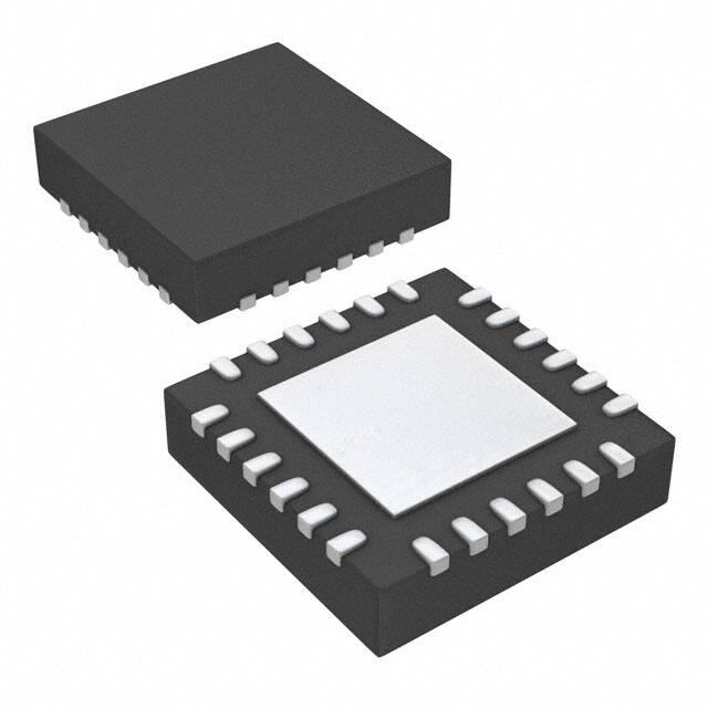
Small Footprint: 4-mm × 4-mm VQFN
The ADS89xxB boosts analog performance while
maintaining high-resolution data transfer by using TI’s
Enhanced-SPI feature. Enhanced-SPI enables
ADS89xxB in achieving high throughput at lower
clock speeds, there by simplifying the board layout
and lowering system cost. Enhanced-SPI also
simplifies the host’s clocking-in of data there by
making it ideal for applications involving FPGAs,
DSPs. ADS89xxB is compatible with standard SPI
Interface.
The ADS89xxB has an internal data parity feature
which can be appended to the ADC data output. ADC
data validation by the host, using parity bits, improves
system reliability.
SPI Interface Clock at 1 MSPS
DEVICE
RESOLUTION
2 Applications
•
•
•
Test and Measurement
Medical Imaging
High-Precision, High-Speed Data Acquisition
3-WIRE
ENHANCED SPI
3-WIRE SPI
20 bits
70 MHz
22 MHz
18 bits
58 MHz
20 MHz
16 bits
52 MHz
18 MHz
(1) For all features of the enhanced SPI, see the Interface
Module section.
Ease of System Design with ADS89xxB Integrated Features
Multi-ADC System with Single Supply
and Reference
Lowest Clock Speeds at 1-MSPS using 3-Wire EnhancedSPI
ADS89xxB
VREF
AINP
REFBUF
REFBUF
OUT
OUT
REFBUFOUT
AINP
AINP
AINP
AINM
AINM
AINM
REFIN
BUF REFIN
BUF REFIN
BUF
DVDD
DVDD
DVDD
Parity
ADS890xB
ADS890xB
ADS89xxB
DECAP
RVDD
RVDD
AVDD
CS
CS
AINM
Parity
AINM
AVDD
ADC Conversion
SDI
SDO
SCLK
Quiet time
ADC Data SPI
ADC
SPI
ADC
MCU
CONV
Data
Data
Read
SPI
70-MHz
22-MHz
SCK
ISO
ADC Conversion
Enhanced SPI (Data + Parity)
22-MHz
1
An IMPORTANT NOTICE at the end of this data sheet addresses availability, warranty, changes, use in safety-critical applications,
intellectual property matters and other important disclaimers. PRODUCTION DATA.
�ADS8900B, ADS8902B, ADS8904B
SBAS728A – NOVEMBER 2016 – REVISED JUNE 2017
www.ti.com
Table of Contents
1
2
3
4
5
6
Features ..................................................................
Applications ...........................................................
Description .............................................................
Revision History.....................................................
Pin Configuration and Functions .........................
Specifications.........................................................
6.1
6.2
6.3
6.4
6.5
6.6
6.7
6.8
7
1
1
1
2
3
5
Absolute Maximum Ratings ..................................... 5
ESD Ratings.............................................................. 5
Recommended Operating Conditions....................... 5
Thermal Information .................................................. 5
Electrical Characteristics........................................... 6
Timing Requirements ................................................ 8
Switching Characteristics .......................................... 9
Typical Characteristics ............................................ 13
Detailed Description ............................................ 18
7.1
7.2
7.3
7.4
Overview .................................................................
Functional Block Diagram .......................................
Feature Description.................................................
Device Functional Modes........................................
18
18
19
25
7.5 Programming........................................................... 27
7.6 Register Maps ......................................................... 51
8
Application and Implementation ........................ 57
8.1 Application Information............................................ 57
8.2 Typical Application .................................................. 59
9 Power-Supply Recommendations...................... 64
10 Layout................................................................... 65
10.1 Layout Guidelines ................................................. 65
10.2 Layout Example .................................................... 66
11 Device and Documentation Support ................. 67
11.1
11.2
11.3
11.4
11.5
11.6
11.7
Documentation Support ........................................
Related Links ........................................................
Receiving Notification of Documentation Updates
Community Resources..........................................
Trademarks ...........................................................
Electrostatic Discharge Caution ............................
Glossary ................................................................
67
67
67
67
68
68
68
12 Mechanical, Packaging, and Orderable
Information ........................................................... 68
4 Revision History
NOTE: Page numbers for previous revisions may differ from page numbers in the current version.
Changes from Original (November 2016) to Revision A
Page
•
Changed SPI Interface Clock at 1 MSPS table...................................................................................................................... 1
•
Changed DVDD specified throughput value in the Recommended Operating Conditions from 3.6 V to 5.5 V....................... 5
•
Changed maximum value for DVDD range in Electrical Characteristics, Timing Requirements, and Switching
Characteristics from 3.6 V to 5.5 V......................................................................................................................................... 6
•
Added TA = 25°C to reference buffer offset voltage test condition in Electrical Characteristics table ................................... 6
•
Changed input offset thermal drift typ value from 10 to 1 ...................................................................................................... 6
•
Added fIN = 2 kHz test condition to SFDR in Electrical Characteristics table ........................................................................ 7
•
Changed DAQ Circuit With FDA Input Driver and Single-Ended or Differential Input section for clarity ............................. 61
2
Submit Documentation Feedback
Copyright © 2016–2017, Texas Instruments Incorporated
Product Folder Links: ADS8900B ADS8902B ADS8904B
�ADS8900B, ADS8902B, ADS8904B
www.ti.com
SBAS728A – NOVEMBER 2016 – REVISED JUNE 2017
5 Pin Configuration and Functions
CS
SCLK
SDI
RVS
SDO-0
SDO-1
24
23
22
21
20
19
RGE Package
24-Pin VQFN
Top View
CONVST
1
18
SDO-2
RST
2
17
SDO-3
REFIN
3
16
DVDD
REFM
4
15
GND
REFBUFOUT
5
14
DECAP
NC
6
13
DECAP
Thermal
7
8
9
10
11
12
REFBUFOUT
REFM
AINP
AINM
GND
RVDD
Pad
Not to scale
Pin Functions
PIN
NO.
FUNCTION
AINM
NAME
10
Analog input
Negative analog input
AINP
9
Analog input
Positive analog input
CS
24
Digital input
Chip-select input pin; active low
The device takes control of the data bus when CS is low.
The SDO-x pins go to Hi-Z when CS is high.
CONVST
1
Digital input
Conversion start input pin.
A CONVST rising edge brings the device from ACQ state to CNV state.
13, 14
Power supply
Place decoupling capacitor here for internal power supply. Short pin 13 and 14 together.
16
Power supply
Interface power supply pin
11, 15
Power supply
Ground
No connection
Float these pins; no external connection.
DECAP
DVDD
GND
NC
REFBUFOUT
6
5, 7
DESCRIPTION
Analog input/output Internal reference buffer output, external reference input. Short pin 5 and 7 together.
REFIN
3
Analog input
Reference voltage input
REFM
4, 8
Analog input
Reference ground potential
RST
2
Digital input
Asynchronous reset input pin.
A low pulse on the RST pin resets the device. All register bits return to the default state.
RVDD
12
Power supply
Analog power supply pin.
RVS
21
Digital output
Multifunction output pin.
With CS held high, RVS reflects the status of the internal ADCST signal.
With CS low, the status of RVS depends on the output protocol selection.
SCLK
23
Digital input
Clock input pin for the serial interface.
All system-synchronous data transfer protocols are timed with respect to the SCLK signal.
SDI
22
Digital input
Serial data input pin.
This pin is used to feed data or commands into the device.
Copyright © 2016–2017, Texas Instruments Incorporated
Product Folder Links: ADS8900B ADS8902B ADS8904B
Submit Documentation Feedback
3
�ADS8900B, ADS8902B, ADS8904B
SBAS728A – NOVEMBER 2016 – REVISED JUNE 2017
www.ti.com
Pin Functions (continued)
PIN
NAME
NO.
FUNCTION
SDO-0
20
Digital output
Serial communication pin: data output 0
SDO-1
19
Digital output
Serial communication pin: data output 1
SDO-2
18
Digital output
Serial communication pin: data output 2
SDO-3
17
Digital output
Serial communication pin: data output 3
Supply
Exposed thermal pad; connect to GND.
Thermal pad
4
Submit Documentation Feedback
DESCRIPTION
Copyright © 2016–2017, Texas Instruments Incorporated
Product Folder Links: ADS8900B ADS8902B ADS8904B
�ADS8900B, ADS8902B, ADS8904B
www.ti.com
SBAS728A – NOVEMBER 2016 – REVISED JUNE 2017
6 Specifications
6.1
Absolute Maximum Ratings
over operating free-air temperature range (unless otherwise noted) (1)
MIN
MAX
UNIT
RVDD to GND
–0.3
7
V
DVDD to GND
–0.3
7
V
REFIN to REFM
–0.3
RVDD + 0.3
V
REFM to GND
–0.1
0.1
V
Analog Input (AINP, AINM) to GND
–0.3
VREF + 0.3
V
Digital input (RST, CONVST, CS, SCLK, SDI) to GND
–0.3
DVDD + 0.3
V
Digital output (READY, SDO-0, SDO-1, SDO-2, SDO-3) to GND
–0.3
DVDD + 0.3
V
Analog Input (AINP, AINM) to RVDD and GND
–130
130
mA
Operating free-air temperature, TA
–40
125
°C
Storage temperature, Tstg
–65
150
°C
(1)
Stresses beyond those listed under Absolute Maximum Ratings may cause permanent damage to the device. These are stress ratings
only, which do not imply functional operation of the device at these or any other conditions beyond those indicated under Recommended
Operating Conditions. Exposure to absolute-maximum-rated conditions for extended periods may affect device reliability.
6.2 ESD Ratings
VALUE
V(ESD)
(1)
(2)
Electrostatic discharge
Human-body model (HBM), per ANSI/ESDA/JEDEC JS-001 (1)
±2000
Charged-device model (CDM), per JEDEC specification JESD22-C101 (2)
±500
UNIT
V
JEDEC document JEP155 states that 500-V HBM allows safe manufacturing with a standard ESD control process.
JEDEC document JEP157 states that 250-V CDM allows safe manufacturing with a standard ESD control process.
6.3 Recommended Operating Conditions
over operating free-air temperature range (unless otherwise noted)
RVDD
MIN
NOM
MAX
3
5
5.5
Operating
1.65
3
5.5
Specified throughput
2.35
3
5.5
Analog supply voltage (RVDD to AGND)
DVDD
Digital supply voltage (DVDD to AGND)
VREF
Reference input voltage on REFIN
2.5
CREFBUF
External ceramic decoupling capacitor
10
RESR
External series resistor
TA
Specified free-air operating temperature
RVDD – 0.3
22
UNIT
V
V
V
µF
0
1
1.3
Ω
–40
25
125
°C
6.4 Thermal Information
ADS890xB
THERMAL METRIC (1)
RGE (VQFN)
UNITS
24 PINS
RθJA
Junction-to-ambient thermal resistance
31.9
°C/W
RθJC(top)
Junction-to-case (top) thermal resistance
29.9
°C/W
RθJB
Junction-to-board thermal resistance
8.9
°C/W
ψJT
Junction-to-top characterization parameter
0.3
°C/W
ψJB
Junction-to-board characterization parameter
8.9
°C/W
RθJC(bot)
Junction-to-case (bottom) thermal resistance
2.0
°C/W
(1)
For more information about traditional and new thermal metrics, see the Semiconductor and IC Package Thermal Metrics application
report.
Copyright © 2016–2017, Texas Instruments Incorporated
Product Folder Links: ADS8900B ADS8902B ADS8904B
Submit Documentation Feedback
5
�ADS8900B, ADS8902B, ADS8904B
SBAS728A – NOVEMBER 2016 – REVISED JUNE 2017
www.ti.com
6.5 Electrical Characteristics
At RVDD = 5.5 V, DVDD = 1.65 V to 5.5 V, VREF = 5 V, and maximum throughput (unless otherwise noted).
Minimum and maximum values at TA = –40°C to +125°C; typical values at TA = 25°C.
PARAMETER
TEST CONDITIONS
MIN
TYP
MAX
UNIT
–VREF
VREF
V
0
VREF
V
(VREF / 2) +
0.1
V
ANALOG INPUT
FSR
Full-scale input range
(AINP – AINM)
VIN
Absolute input voltage
(AINP and AINM to REFM)
VCM
Common-mode voltage
(AINP + AINM) / 2
CIN
Input capacitance
(VREF / 2) –
0.1
Sample mode
VREF / 2
60
pF
Hold mode
4
pF
VREF = 5 V
0.1
VOLTAGE REFERENCE INPUT (REFIN)
IREF
Reference input current
CREF
Internal capacitance
1
10
µA
pF
REFERENCE BUFFER OUTPUT (REFBUFOUT)
V(RO)
Reference buffer offset voltage
With EN_MARG = 0b (1), TA = 25°C (2)
(VREFBUFOUT – VREF)
CREFBUF
External ceramic decoupling
capacitor
RESR
External series resistor
ISHRT
Short-circuit current
–250
10
0
250
22
1
µV
µF
1.3
Ω
30
mA
Margining range
With EN_MARG = 1b (1)
±4.5
mV
Margining resolution
With EN_MARG = 1b (1)
280
µV
20
Bits
DC ACCURACY (3) (CREFBUF = 22 µF, RESR = 1 Ω)
Resolution
NMC
No missing codes
20
TA = 0°C to +60°C
±1
2
TA = –40°C to +85°C
-2.75
±1
2.75
TA = –40°C to +125°C
-3.75
±1
3.75
-0.5
±0.2
0.5
-11.5
±3
11.5
-60
±10
60
-0.03
±0.005
INL
Integral nonlinearity (4)
DNL
Differential nonlinearity (4)
E(IO)
Input offset error (4)
dVOS/dT
Input offset thermal drift (2)
GE
Gain error (4)
EN_MARG = 0b (1) (6)
dGE/dT
Gain error thermal drift
EN_MARG = 0b (1) (6)
TNS
Transition noise
CMRR
Bits
-2
TA = 25°C (2)
TA = –40°C to +125°C
(2)
1
First output code deviation for
burst-mode data acquisition
See Reference Buffer Module
Common-mode rejection ratio
dc to 20 kHz
ppm (5)
ppm (5)
ppm (5)
μV/°C
0.03
%FSR
3.6
ppm/°C
2.3
ppm (5)
–3
3
TNS
80
dB
4
ns
2
ps RMS
23
MHz
SAMPLING DYNAMICS
Aperture delay
tj-rms
Aperture jitter
f3-DB(small)
Small-signal bandwidth
(1)
(2)
(3)
(4)
(5)
(6)
6
See the REF_MRG Register.
For selected VREF, see the OFST_CAL Register.
While operating with internal reference buffer and LDO.
See for statistical distribution data for DNL, INL, offset, and gain error parameters.
LSB = least-significant bit. 1 LSB at 20-bit resolution is approximately 0.95 ppm.
Includes internal reference buffer errors and drifts.
Submit Documentation Feedback
Copyright © 2016–2017, Texas Instruments Incorporated
Product Folder Links: ADS8900B ADS8902B ADS8904B
�ADS8900B, ADS8902B, ADS8904B
www.ti.com
SBAS728A – NOVEMBER 2016 – REVISED JUNE 2017
Electrical Characteristics (continued)
At RVDD = 5.5 V, DVDD = 1.65 V to 5.5 V, VREF = 5 V, and maximum throughput (unless otherwise noted).
Minimum and maximum values at TA = –40°C to +125°C; typical values at TA = 25°C.
PARAMETER
TEST CONDITIONS
MIN
TYP
fIN = 2 kHz, TA = –40°C to +85°C
101.8
103.9
fIN = 2 kHz, TA = –40°C to +125°C
101.3
103.9
102
104.5
101.5
104.5
MAX
UNIT
AC ACCURACY (3) (7) (CREFBUF = 22 µF, RESR = 1 Ω)
SINAD
Signal-to-noise + distortion
fIN = 2 kHz, TA = –40°C to +85°C
SNR
Signal-to-noise ratio
fIN = 2 kHz, TA = –40°C to +125°C
THD
Total harmonic distortion
SFDR
Spurious-free dynamic range
fIN = 100 kHz
99.5
fIN = 2 kHz
–125
fIN = 100 kHz
–110
fIN = 2 kHz
dB
dB
dB
125
dB
2.85
V
LDO OUTPUT (DECAP)
VLDO
LDO output voltage
(DECAP pins)
CLDO
External ceramic capacitor on
DECAP pins
tPU_LDO
LDO power-up time
ISHRT-LDO
Short-circuit current
1
CLDO = 1 µF, RVDD > VLDO
µF
1
ms
100
mA
DIGITAL INPUTS
VIH
High-level input voltage
VIL
Low-level input voltage
1.65 V < DVDD < 2.3 V
0.8 DVDD
DVDD + 0.3
2.3 V < DVDD < 5.5 V
0.7 DVDD
DVDD + 0.3
1.65 V < DVDD < 2.3 V
–0.3
0.2 DVDD
2.3 V < DVDD < 5.5 V
–0.3
0.3 DVDD
Input current
±0.01
V
V
0.1
μA
0.8 DVDD
DVDD
V
0
0.2 DVDD
V
DIGITAL OUTPUTS
VOH
High-level output voltage
IOH = 500-µA source
VOL
Low-level output voltage
IOH = 500-µA sink
POWER SUPPLY
IRVDD
Analog supply current
ADS8900B at RVDD = 5 V, 1-MSPS
4.2
5.8
mA
ADS8902B at RVDD = 5 V, 500-KSPS
3.2
4
mA
ADS8904B at RVDD = 5 V, 250-KSPS
2.8
3.6
mA
Static, no conversion
970
μA
Static, PD_ADC = 1b (8)
900
μA
120
μA
40
μA
1
μA
Static, PD_REFBUF = 1b
(8)
Static, PD_ADC = 1b and
PD_REFBUF = 1b (8)
IDVDD
Digital supply current
PRVDD
Power dissipation
(7)
(8)
DVDD = 3 V, CLOAD = 10 pF, no
conversion
ADS8900B at RVDD = 5 V, 1-MSPS
21
29
ADS8902B at RVDD = 5 V, 500-KSPS
16
20
ADS8904B at RVDD = 5 V, 250-KSPS
14
18
mW
For VIN = –0.1 dBFS.
See the PD_CNTL Register.
Copyright © 2016–2017, Texas Instruments Incorporated
Product Folder Links: ADS8900B ADS8902B ADS8904B
Submit Documentation Feedback
7
�ADS8900B, ADS8902B, ADS8904B
SBAS728A – NOVEMBER 2016 – REVISED JUNE 2017
www.ti.com
6.6 Timing Requirements
MIN
TYP
MAX
UNIT
TIMING
DIAGRAM
CONVERSION CYCLE
fcycle
Sampling frequency
tcycle
ADC cycle-time period
ADS8900B
1000
ADS8902B
500
ADS8904B
250
ADS8900B
1
ADS8902B
2
ADS8904B
4
twh_CONVST Pulse duration: CONVST high
twl_CONVST
Pulse duration: CONVST low
tacq
Acquisition time
tqt_acq
td_cnvcap
kHz
µs
30
ns
Figure 1
30
ns
300
ns
Quiet acquisition time
30
ns
Quiet aperture time
20
ns
100
ns
Figure 2
MHz
Figure 3
ns
Figure 3
Figure 46,
see Data
Transfer
Protocols
ASYNCHRONOUS RESET, AND LOW POWER MODES
twl_RST
Pulse duration: RST low
SPI-COMPATIBLE SERIAL INTERFACE
fCLK
Serial clock frequency
2.35 V ≤ DVDD ≤ 5.5 V,
TA = –40°C to +125°C,
VIH > 0.7 DVDD, VIL < 0.3 DVDD
70
1.65 V ≤ DVDD < 2.35 V,
TA = –40°C to +125°C,
VIH > 0.8 DVDD, VIL < 0.2 DVDD
20
1.65 V ≤ DVDD < 2.35 V,
TA = 0°C to +60°C,
VIH > 0.8 DVDD, VIL < 0.2 DVDD
57
1.65 V ≤ DVDD < 2.35 V,
TA = –40°C to +125°C,
VIH > 0.9 DVDD, VIL < 0.1 DVDD
68
tCLK
Serial clock time period
1/fCLK
tph_CK
SCLK high time
0.45
0.55
tCLK
tpl_CK
SCLK low time
0.45
0.55
tCLK
tsu_CSCK
Setup time: CS falling to the first SCLK capture edge
12
ns
tsu_CKDI
Setup time: SDI data valid to the SCLK capture edge
1.5
ns
tht_CKDI
Hold time: SCLK capture edge to (previous) data valid on SDI
1
ns
tht_CKCS
Delay time: last SCLK falling to CS rising
7
ns
Figure 3
SOURCE-SYNCHRONOUS SERIAL INTERFACE (External Clock) (1)
fCLK
tCLK
(1)
8
Serial clock frequency
SDR (DATA_RATE = 0b),
2.35 V ≤ DVDD ≤ 5.5 V
70
DDR (DATA_RATE = 1b),
2.35 V ≤ DVDD ≤ 5.5 V
35
Serial clock time period
MHz
1/fCLK
Figure 4,
see Data
Transfer
Protocols
ns
The external clock option is not recommended when operating with DVDD < 2.35 V. See Table 9.
Submit Documentation Feedback
Copyright © 2016–2017, Texas Instruments Incorporated
Product Folder Links: ADS8900B ADS8902B ADS8904B
�ADS8900B, ADS8902B, ADS8904B
www.ti.com
SBAS728A – NOVEMBER 2016 – REVISED JUNE 2017
6.7 Switching Characteristics
At RVDD = 5.5 V, DVDD = 1.65 V to 5.5 V, VREF = 5 V, and maximum throughput (unless otherwise noted).
Minimum and maximum values at TA = –40°C to +125°C; typical values at TA = 25°C.
PARAMETER
MIN
TYP
MAX
UNIT
TIMING
DIAGRAM
ns
Figure 1
ms
Figure 2
CONVERSION CYCLE
tconv
Conversion time
ADS8900B
600
670
ADS8902B
1100
1200
ADS8904B
2400
2500
ASYNCHRONOUS RESET, AND LOW POWER MODES
td_rst
Delay time: RST rising to RVS rising
tPU_ADC
Power-up time for converter module
tPU_REFBUF Power-up time for internal reference buffer, CREFBUF = 22 µF
tPU_Device
Power-up time for
device
CLDO = 1 µF, CREFBUF = 22 µF
3
1
ms
10
ms
10
ms
See
PD_CNTL
Register
SPI-COMPATIBLE SERIAL INTERFACE
tden_CSDO
Delay time: CS falling to data enable
9
ns
tdz_CSDO
Delay time: CS rising to SDO going to Hi-Z
10
ns
td_CKDO
Delay time: SCLK launch edge to (next) data valid on SDO
13
ns
td_CSRDY_f
Delay time: CS falling to RVS falling
12
ns
Figure 4
td_CSRDY_r
Delay time:
CS rising to RVS rising
ns
Figure 4
After NOP operation
30
After WR or RD operation
120
Figure 3
SOURCE-SYNCHRONOUS SERIAL INTERFACE (External Clock) (1)
td_CKSTR_r
Delay time: SCLK launch edge to RVS rising
13
ns
td_CKSTR_f
Delay time: SCLK launch edge to RVS falling
13
ns
toff_STRDO_f Time offset: RVS falling to (next) data valid on SDO
-2
2
ns
toff_STRDO_r Time offset: RVS rising to (next) data valid on SDO
-2
2
ns
tph_STR
Strobe output high time, 2.35 V ≤ DVDD ≤ 5.5 V
0.45
0.55
tSTR
tpl_STR
Strobe output low time, 2.35 V ≤ DVDD ≤ 5.5 V
0.45
0.55
tSTR
Figure 4
SOURCE-SYNCHRONOUS SERIAL INTERFACE (Internal Clock)
td_CSSTR
Delay time: CS falling to RVS rising
Strobe output time
period
tSTR
15
50
INTCLK option
15
INTCLK / 2 option
30
INTCLK / 4 option
60
ns
ns
tph_STR
Strobe output high time
0.45
0.55
tSTR
tpl_STR
Strobe output low time
0.45
0.55
tSTR
(1)
Figure 5
The external clock option is not recommended when operating with DVDD < 2.35 V. See Table 9.
Copyright © 2016–2017, Texas Instruments Incorporated
Product Folder Links: ADS8900B ADS8902B ADS8904B
Submit Documentation Feedback
9
�ADS8900B, ADS8902B, ADS8904B
SBAS728A – NOVEMBER 2016 – REVISED JUNE 2017
www.ti.com
Sample
S
Sample
S+1
twh_CONVST
twl_CONVST
CONVST
tcycle
tconv_max
tconv
tacq
tconv_min
ADCST (Internal)
CNV (C)
ACQ (C + 1)
CS
RVS
Figure 1. Conversion Cycle Timing
trst
twl_RST
RST
td_rst
CONVST
CS
SCLK
RVS
SDO-x
Figure 2. Asynchronous Reset Timing
10
Submit Documentation Feedback
Copyright © 2016–2017, Texas Instruments Incorporated
Product Folder Links: ADS8900B ADS8902B ADS8904B
�ADS8900B, ADS8902B, ADS8904B
www.ti.com
SBAS728A – NOVEMBER 2016 – REVISED JUNE 2017
tCLK
tph_CK
CS
tpl_CK
(1)
SCLK
tsu_CKDI
tsu_CSCK
tht_CKCS
tht_CKDI
SCLK(1)
SDI
tden_CSDO
tdz_CSDO
td_CKDO
SDO-x
(1)
SDO-x
The SCLK polarity, launch edge, and capture edge depend on the SPI protocol selected.
Figure 3. SPI-Compatible Serial Interface Timing
tCLK
tph_CK
CS
tpl_CK
SCLK
td_CKSTR_f
tsu_CSCK
tht_CKCS
SCLK
td_CKSTR_r
RVS
tden_CSDO
tdz_CSDO
toff_STRDO_f
toff_STRDO_r
SDO-x
(DDR)
SDO-x
td_CSRDY_f
td_CSRDY_r
toff_STRDO_r
SDO-x
(SDR)
RVS
Figure 4. Source-Synchronous Serial Interface Timing (External Clock)
Copyright © 2016–2017, Texas Instruments Incorporated
Product Folder Links: ADS8900B ADS8902B ADS8904B
Submit Documentation Feedback
11
�ADS8900B, ADS8902B, ADS8904B
SBAS728A – NOVEMBER 2016 – REVISED JUNE 2017
www.ti.com
tSTR
RVS
CS
tph_STR
tden_CSDO
tdz_CSDO
toff_STRDO_r
tpl_STR
toff_STRDO_f
SDO-x
(DDR)
SDO-x
td_CSRDY_f
td_CSRDY_r
toff_STRDO_r
SDO-x
(SDR)
RVS
td_CSSTR
Figure 5. Source-Synchronous Serial Interface Timing (Internal Clock)
12
Submit Documentation Feedback
Copyright © 2016–2017, Texas Instruments Incorporated
Product Folder Links: ADS8900B ADS8902B ADS8904B
�ADS8900B, ADS8902B, ADS8904B
www.ti.com
SBAS728A – NOVEMBER 2016 – REVISED JUNE 2017
6.8 Typical Characteristics
at TA = 25°C, RVDD = 5.5 V, DVDD = 3 V, VREF = 5 V, and maximum-rated throughput (unless otherwise noted)
2
Integral Nonlinearity (LSB)
Differential Nonlinearity (LSB)
1
0.5
0
-0.5
-1
-524288
0
-1
-2
-524288
524287
ADC Output Code
1
524287
ADC Output Code
D001
Typical DNL = ±0.2 ppm
Figure 6. Typical DNL
Figure 7. Typical INL
3500
3000
3000
2500
2500
2000
Frequency
Frequency
D002
Typical INL = ±0.75 ppm
2000
1500
1500
1000
1000
500
500
0
0
-0.5 -0.4 -0.3 -0.2 -0.1
0
0.1
0.2
0.3
0.4
0.5
-2
-1.5
-1
-0.5
0
0.5
1
1.5
2
D007
D008
3250 devices
3250 devices
Figure 8. Typical DNL Distribution (LSB)
Figure 9. Typical INL Distribution (LSB)
4
1
Maximum
Minimum
Integral Nonlinearity (LSB)
Differential Nonlinearity (LSB)
Maximum
Minimum
0.5
0
-0.5
-1
-40
-7
26
59
Free-Air Temperature (qC)
92
Figure 10. DNL vs Temperature
125
D003
2
0
-2
-4
-40
-7
26
59
Free-Air Temperature (qC)
92
125
D004
Figure 11. INL vs Temperature
Copyright © 2016–2017, Texas Instruments Incorporated
Product Folder Links: ADS8900B ADS8902B ADS8904B
Submit Documentation Feedback
13
�ADS8900B, ADS8902B, ADS8904B
SBAS728A – NOVEMBER 2016 – REVISED JUNE 2017
www.ti.com
Typical Characteristics (continued)
at TA = 25°C, RVDD = 5.5 V, DVDD = 3 V, VREF = 5 V, and maximum-rated throughput (unless otherwise noted)
3
1
Maximum
Minimum
2
Integral Nonlinearity (LSB)
0.5
0
-0.5
1
0
-1
-2
-1
2.5
3
3.5
4
Reference Voltage (V)
4.5
-3
2.5
5
3
D005
Figure 12. DNL vs Reference Voltage
4.5
5
D006
Figure 13. INL vs Reference Voltage
1400
1200
1200
1000
1000
800
Frequency
800
600
600
400
400
200
200
0
4
6
8
10
D019
3250 devices
0.
00
4
0.
00
6
0.
00
8
0.
01
2
0
0
00
2
-2
0.
-4
.0
1
-6
-0
-8
.0
08
.0
06
-0
.0
04
-0
.0
02
0
-10
-0
Frequency
3.5
4
Reference Voltage (V)
-0
Differential Nonlinearity (LSB)
Maximum
Minimum
D022
3250 devices
Figure 14. Typical Offset Distribution (LSB)
Figure 15. Typical Gain Error Distribution (%FS)
5
10
8
3
6
Offset (mV)
Offset (LSB)
4
2
0
-2
1
-1
-4
-3
-6
-8
-10
-40
-7
26
59
Free-Air Temperature (qC)
92
REF_SEL[2:0] = 000b
Figure 16. Offset vs Temperature
14
Submit Documentation Feedback
125
D020
-5
2.5
3
3.5
4
Reference Voltage (V)
4.5
5
D021
With appropriate REF_SEL[2:0], see OFST_CAL
Figure 17. Offset vs Reference Voltage
Copyright © 2016–2017, Texas Instruments Incorporated
Product Folder Links: ADS8900B ADS8902B ADS8904B
�ADS8900B, ADS8902B, ADS8904B
www.ti.com
SBAS728A – NOVEMBER 2016 – REVISED JUNE 2017
Typical Characteristics (continued)
at TA = 25°C, RVDD = 5.5 V, DVDD = 3 V, VREF = 5 V, and maximum-rated throughput (unless otherwise noted)
0.02
0.1
Gain (%FS) ADC only
Gain (%FS) ADC + REFBUF
Gain (%FS) ADC only
Gain (%FS) ADC + REFBUF
0.012
Gain Error (%FS)
Gain Error (%FS)
0.05
0.004
-0.004
0
-0.05
-0.012
-0.02
-40
-7
26
59
Free-Air Temperature (qC)
92
-0.1
2.5
125
3
D023
EN_MARG = 0b
600
-50
Power (dB)
0
400
7
52
42
89
52
42
91
52
42
93
52
42
95
52
42
97
52
42
8
52
42
8
52
42
8
5
-200
3
0
1
-150
52
42
8
D024
-100
200
52
42
7
5
Figure 19. Gain Error vs Reference Voltage
800
9
Frequency
4.5
EN_MARG = 0b
Figure 18. Gain Error vs Temperature
0
100
D009
Standard Deviation = 2 ppm
fIN = 2 kHz
Figure 20. DC Input Histogram
200
300
fIN, Input Frequency (kHz)
SNR = 104.5 dB
400
500
D011
THD = –125 dB
Figure 21. Typical FFT - ADS8900B
0
0
-50
-50
Power (dB)
Power (dB)
3.5
4
Reference Voltage (V)
-100
-150
-100
-150
-200
-200
0
fIN = 2 kHz
50
100
150
fIN, Input Frequency (kHz)
SNR = 104.5 dB
200
250
0
D029
THD = –125 dB
Figure 22. Typical FFT - ADS8902B
fIN = 2 kHz
25
50
75
fIN, Input Frequency (kHz)
SNR = 104.5 dB
100
125
D030
THD = –125 dB
Figure 23. Typical FFT - ADS8904B
Copyright © 2016–2017, Texas Instruments Incorporated
Product Folder Links: ADS8900B ADS8902B ADS8904B
Submit Documentation Feedback
15
�ADS8900B, ADS8902B, ADS8904B
SBAS728A – NOVEMBER 2016 – REVISED JUNE 2017
www.ti.com
Typical Characteristics (continued)
at TA = 25°C, RVDD = 5.5 V, DVDD = 3 V, VREF = 5 V, and maximum-rated throughput (unless otherwise noted)
106
-116
18
132
104
17
103
16.5
26
59
Free-Air Temperature (qC)
92
128
-124
124
-128
120
-132
-40
16
125
-7
26
59
Free-Air Temperature (qC)
D013
fIN = 2 kHz
92
D014
fIN = 2 kHz
Figure 24. Noise Performance vs Temperature
108
Figure 25. Distortion Performance vs Temperature
-116
17.5
132
THD
SFDR
128
-124
124
16
-128
120
15.5
-132
2.5
17
100
16.5
96
3
3.5
4
Reference Voltage (V)
4.5
THD (dBFS)
-120
104
ENOB (Bits)
SNR, SINAD (dBFS)
SNR
SINAD
ENOB
92
2.5
5
116
3
3.5
4
Reference Voltage (V)
D015
fIN = 2 kHz
Figure 26. Noise Performance vs Reference Voltage
95
15
90
14
THD (dBFS)
16
ENOB (Bits)
100
D016
-90
130
-95
125
-100
120
-105
115
-110
110
-115
105
-120
100
-125
85
100
200
300
fIN, Input Frequency (kHz)
400
13
500
D017
Figure 28. Noise Performance vs Input Frequency
16
Submit Documentation Feedback
5
Figure 27. Distortion Performance vs Reference Voltage
17
SNR
SINAD
ENOB
SNR, SINAD (dBFS)
4.5
fIN = 2 kHz
105
0
116
125
SFDR (dBFS)
-7
-120
-130
0
100
200
300
fIN, Input Frequency (kHz)
400
SFDR (dBFS)
102
-40
THD (dBFS)
SNR, SINAD (dBFS)
17.5
ENOB (Bits)
105
SFDR (dBFS)
THD
SFDR
SNR
SINAD
ENOB
95
THD
SFDR
90
500
D018
Figure 29. Distortion Performance vs Input Frequency
Copyright © 2016–2017, Texas Instruments Incorporated
Product Folder Links: ADS8900B ADS8902B ADS8904B
�ADS8900B, ADS8902B, ADS8904B
www.ti.com
SBAS728A – NOVEMBER 2016 – REVISED JUNE 2017
Typical Characteristics (continued)
at TA = 25°C, RVDD = 5.5 V, DVDD = 3 V, VREF = 5 V, and maximum-rated throughput (unless otherwise noted)
5
5.5
ADS8900B
ADS8902B
ADS8904B
5
4.5
4
IRVDD (mA)
IRVDD (mA)
4
3.5
3
3
2
2.5
2
1
ADS8900B
ADS8902B
ADS8904B
1.5
1
3
3.5
4
4.5
RVDD (V)
5
5.5
D026
0
-40
-7
26
59
Free-Air Temperature (qC)
92
125
D028
RVDD = 5 V
Figure 30. Analog Supply Current vs Supply Voltage
Figure 31. Analog Supply Current vs Temperature
Copyright © 2016–2017, Texas Instruments Incorporated
Product Folder Links: ADS8900B ADS8902B ADS8904B
Submit Documentation Feedback
17
�ADS8900B, ADS8902B, ADS8904B
SBAS728A – NOVEMBER 2016 – REVISED JUNE 2017
www.ti.com
7 Detailed Description
7.1 Overview
The ADS890xB is a family of high-speed, successive approximation register (SAR), analog-to-digital converters
(ADC) based on a charge redistribution architecture. These compact devices integrate a reference buffer and
LDO, and feature high performance at a high throughput rate with low power consumption.
This device family supports unipolar, fully differential, analog input signals. The integrated reference buffer
supports the burst mode of data acquisition for external reference voltages in the range 2.5 V to 5 V, and offers a
wide selection of input ranges without additional input scaling.
When a conversion is initiated, the differential input between the AINP and AINM pins is sampled on the internal
capacitor array. The device uses an internal clock to perform conversions. During the conversion process, both
analog inputs are disconnected from the internal circuit. At the end of conversion process, the device reconnects
the sampling capacitors to the AINP and AINM pins and enters an acquisition phase.
The integrated LDO allows the device to operate on a single supply, RVDD. The device consumes only 21 mW,
16 mW, or 14 mW of power when operating at the rated maximum throughput of 1 MSPS, 500 kSPS, or 250
kSPS, respectively, with the internal reference buffer and LDO enabled.
The enhanced multiSPI digital interface is backward-compatible with traditional SPI protocol. Configurable
features simplify board layout, timing, and firmware, and support high throughput at lower clock speeds, thus
allowing an easy interface with a variety of microcontrollers, DSPs, and FPGAs.
The ADS890xB enables test and measurement, medical, and industrial applications to achieve fast, low-noise,
low-distortion, low-power data acquisition in small form factors.
7.2 Functional Block Diagram
REFIN
REFBUFOUT
BUF
REFM
RVDD
LDO
DVDD
DECAP
multiSPITM
Digital
Interface
AINP
SAR ADC
AINM
To
Digital
Host
GND
18
Submit Documentation Feedback
Copyright © 2016–2017, Texas Instruments Incorporated
Product Folder Links: ADS8900B ADS8902B ADS8904B
�ADS8900B, ADS8902B, ADS8904B
www.ti.com
SBAS728A – NOVEMBER 2016 – REVISED JUNE 2017
7.3 Feature Description
From a functional perspective, the device comprises four modules: the low-dropout regulator (LDO), the
reference buffer (BUF), the converter (SAR ADC), and the interface (multiSPI digital interface), as shown in the
Functional Block Diagram section.
The LDO module is powered by the RVDD supply, and generates the bias voltage for internal circuit blocks of the
device. The reference buffer module buffers the external reference voltage source from the dynamic, capacitive
switching load present on the reference pins during the conversion process. The converter module samples and
converts the analog input into an equivalent digital output code. The interface module facilitates communication
and data transfer between the device and the host controller.
7.3.1 LDO Module
To enable single-supply operation, the device features an internal low-dropout regulator (LDO). The LDO is
powered by the RVDD supply, and the output is available on the two DECAP pins. This LDO output powers the
critical analog blocks within the device, and must not be used for any other external purposes.
Short the two DECAP pins together, and decouple with the GND pin by placing a 1-μF, X7R-grade, ceramic
capacitor with a 10-V rating, as shown in Figure 32. There is no upper limit on the value of the decoupling
capacitor; however, a larger decoupling capacitor results in a longer power-up time for the device. See the
Layout section for layout recommendations.
RVDD
DECAP
LDO
DECAP
GND
CLDO
1 F
Figure 32. Internal LDO Connections
7.3.2 Reference Buffer Module
On the CONVST rising edge, the device moves from ACQ state to CONV state, and the internal capacitors are
switched to the REFBUFOUT pins as per the successive approximation algorithm. Most of the switching charge
required during the conversion process is provided by external decoupling capacitor CREFBUF. If the charge lost
from the CREFBUF is not replenished before the next CONVST rising edge, the voltage on REFBUFOUT pins is
less than VREFBUFOUT. The subsequent conversion occurs with this different reference voltage, and causes a
proportional error in the output code. The internal reference buffer of the device maintains the voltage on
REFBUFOUT pins within 0.5-LSB of VREFBUFOUT. All the performance characteristics of the device are specified
with the internal reference buffer and specified values of CREFBUF and RESR.
In burst-mode of operation, the device stays in ACQ state for a long duration of time and then performs a burst of
conversions. During the acquisition state (ACQ), the sampling capacitor (CS) is connected to the differential input
pins and no charge is drawn from the REFBUFOUT pins. However, during the very first conversion cycle, there
is a step change in the current drawn from the REFBUFOUT pins. This sudden change in load triggers a
transient settling response in the reference buffer. For a fixed input voltage, any transient settling error at the end
of the conversion cycle results in a change in output codes over the subsequent conversions, as shown in
Figure 33. The internal reference buffer of the ADS89xxB, when used with the recommended values of CREFBUF
and RESR, keeps the transient settling error at the end of each conversion cycle within 0.5-LSB. Therefore, the
device supports burst-mode of operation with every conversion result being as per the datasheet specifications.
Copyright © 2016–2017, Texas Instruments Incorporated
Product Folder Links: ADS8900B ADS8902B ADS8904B
Submit Documentation Feedback
19
�ADS8900B, ADS8902B, ADS8904B
SBAS728A – NOVEMBER 2016 – REVISED JUNE 2017
www.ti.com
Feature Description (continued)
10
With External Se ries Reference Directly Driving SA R ADC
Dev iation From Final Value (LSB)
With External Reference Buffe r Driving SAR ADC
5
With ADS8 90xB Interna l Reference Buffer
0
-5
-10
-15
0
100
200
300
400
500
600
700
800
900
100 0
Time (µs)
Figure 33. ADC Output Codes in Burst-Mode Operation With Various ADC Reference Buffers
Figure 34 shows the block diagram of the internal reference buffer.
ADS89xxB
RVDD
±
BUF
REFIN
REFBUFOUT
+
REFBUFOUT
Margin
REFM
GND
REFM
Figure 34. Internal Reference Buffer Block Diagram
The input range for the device is set by the external voltage applied at the REFIN pin (VREF). The REFIN pin has
electrostatic discharge (ESD) protection diodes to the RVDD and GND pins. For minimum input offset error (see
E(IO) specified in the Electrical Characteristics), set the REF_SEL[2:0] bits to the value closest to VREF (see the
OFST_CAL register).
The internal reference buffer has a typical gain of 1 V/V with minimal offset error (see V(RO) specified in the
Electrical Characteristics), and the output of the buffer is available between the REFBUFOUT pins and the REFM
pins. Set the REF_OFST[4:0] bits to add or subtract an intentional offset voltage (see the REF_MRG register).
Figure 35 shows the external connections required for the internal reference buffer.
20
Submit Documentation Feedback
Copyright © 2016–2017, Texas Instruments Incorporated
Product Folder Links: ADS8900B ADS8902B ADS8904B
�ADS8900B, ADS8902B, ADS8904B
www.ti.com
SBAS728A – NOVEMBER 2016 – REVISED JUNE 2017
Feature Description (continued)
+VA
RVDD
External
Reference
Source
ADS89xxB
-
IREF
VREF
REFBUFOUT
BUF
REFIN
+
RREF_FLT
REFBUFOUT
Margin
CREF_FLT
RESR
REFM
CREFBUF
REFM
GND
Figure 35. External Connections for the Internal Reference Buffer
Select RREF_FLT and CREF_FLT to limit the broadband noise contribution from the external reference source. The
device takes very little current, IREF, from the REFIN pin (typically, 0.1 µA). However, this current flows through
RREF_FLT and may result in additional gain error.
Short the two REFBUFOUT pins externally. Short the two REFM pins to GND externally. As shown in Figure 35,
place a combination of RESR and CREFBUF (see the Electrical Characteristics) between the REFBUFOUT pins and
the REFM pins as close to the device as possible. See the Layout section for layout recommendations.
7.3.3 Converter Module
As shown in Figure 36, the converter module samples the analog input signal (provided between the AINP and
AINM pins), compares this signal with the reference voltage (between the pair of REFBUFOUT and REFM pins),
and generates an equivalent digital output code.
The converter module receives RST and CONVST inputs from the interface module, and outputs the ADCST
signal and the conversion result back to the interface module.
REFP
DVDD
AVDD
RST
OSC
CONVST
CS
RST
AINP
AINM
SCLK
CONVST
Sampleand-Hold
Circuit
ADCST
ADC
SDI
Interface
Module
Conversion
Result
SDO-1
SDO-2
SDO-3
AGND
RVS
Converter Module
REFM
SDO-0
DGND
GND
Figure 36. Converter Module
Copyright © 2016–2017, Texas Instruments Incorporated
Product Folder Links: ADS8900B ADS8902B ADS8904B
Submit Documentation Feedback
21
�ADS8900B, ADS8902B, ADS8904B
SBAS728A – NOVEMBER 2016 – REVISED JUNE 2017
www.ti.com
Feature Description (continued)
7.3.3.1 Sample-and-Hold Circuit
These devices support unipolar, fully differential, analog input signals. Figure 37 shows a small-signal equivalent
circuit of the sample-and-hold circuit. Each sampling switch is represented by a resistance (RS1 and RS2, typically
50 Ω) in series with an ideal switch (SW1 and SW2). The sampling capacitors, CS1 and CS2, are typically 60 pF.
RS1
SW1
AINP
4 pF
CS1
REFBUFOUT
4 pF
CS2
GND
RS2
GND
SW2
AINM
Device in Hold Mode
Figure 37. Input Sampling Stage Equivalent Circuit
During the acquisition process (ACQ state), both positive and negative inputs are individually sampled on CS1
and CS2, respectively. During the conversion process (CNV state), the device converts for the voltage difference
between the two sampled values: VAINP – VAINM.
Each analog input pin has electrostatic discharge (ESD) protection diodes to REFBUFOUT and GND. Keep the
analog inputs within the specified range to avoid turning the diodes on.
Equation 1 and Equation 2 show the full-scale input range (FSR) and common-mode voltage (VCM), respectively,
supported at the analog inputs for any external reference voltage provided on the REFIN pin (VREF).
FSR r VREF
(1)
VCM
22
§ VREF ·
¨ 2 ¸ r 0.1 V
©
¹
Submit Documentation Feedback
(2)
Copyright © 2016–2017, Texas Instruments Incorporated
Product Folder Links: ADS8900B ADS8902B ADS8904B
�ADS8900B, ADS8902B, ADS8904B
www.ti.com
SBAS728A – NOVEMBER 2016 – REVISED JUNE 2017
Feature Description (continued)
7.3.3.2 Internal Oscillator
The device family features an internal oscillator (OSC) that provides the conversion clock; see Figure 36. The
conversion duration is bound by the minimum and maximum value of tconv, as specified in the Switching
Characteristics table.
The interface module uses this internal clock (OSC), an external clock (provided by the host controller on the
SCLK pin), or a combination of both the internal and external clocks, to execute the data transfer operations
between the device and host controller; see the Interface Module section for more details.
7.3.3.3 ADC Transfer Function
The device family supports unipolar, fully differential analog inputs. The device output is in two's compliment
format. Figure 38 and Table 1 show the ideal transfer characteristics for the device.
The least significant bit (LSB) for the ADC is given by Equation 3:
1 LSB
FSR
20
2
2u
VREF
220
(3)
ADC Code (Hex)
7FFFF
00000
FFFFF
80001
80000
VIN
±VREF + 1 LSB
±1 LSB 0
VREF ± 1 LSB
Differential Analog Input
(AINP AINM)
Figure 38. Differential Transfer Characteristics
Table 1. Transfer Characteristics
DIFFERENTIAL ANALOG INPUT VOLTAGE
(AINP – AINM)
OUTPUT CODE
(HEX)
< –VREF
80000
–VREF + 1 LSB
80001
–1 LSB
FFFFF
0
00000
1 LSB
00001
> VREF – 1 LSB
7FFFF
Copyright © 2016–2017, Texas Instruments Incorporated
Product Folder Links: ADS8900B ADS8902B ADS8904B
Submit Documentation Feedback
23
�ADS8900B, ADS8902B, ADS8904B
SBAS728A – NOVEMBER 2016 – REVISED JUNE 2017
www.ti.com
7.3.4 Interface Module
The interface module facilitates the communication and data transfer between the device and the host controller.
As shown in Figure 39, the module consists of shift registers (both input and output), configuration registers, and
a protocol unit.
Shift Registers
RST
Output Data Register (ODR)
D21
D20
D1
CONVST
D0
CS
22 Bits
SCLK
Converter Module
B21
B20
B1
Protocol
22 Bits
B0
Input Data Register (IDR)
SDI
SDO-0
SDO-1
SDO-2
Command Processor
SCLK
Counter
Configuration Registers
SDO-3
RVS
Interface Module
Figure 39. Interface Module
The Pin Configuration and Functions section provides descriptions of the interface pins. The Data Transfer
Frame section details the functions of shift registers, the SCLK counter, and the command processor. The Data
Transfer Protocols section details supported protocols. The Register Maps section explains the configuration
registers and bit settings.
24
Submit Documentation Feedback
Copyright © 2016–2017, Texas Instruments Incorporated
Product Folder Links: ADS8900B ADS8902B ADS8904B
�ADS8900B, ADS8902B, ADS8904B
www.ti.com
SBAS728A – NOVEMBER 2016 – REVISED JUNE 2017
7.4 Device Functional Modes
As shown in Figure 40, this device family supports three functional states: RST, ACQ, and CNV. The device
state is determined by the status of the CONVST and RST control signals provided by the host controller.
Power Up
ACQ
RST Rising Edge
CONVST Rising Edge
RST Falling Edge
End of Conversion
CNV
RST
RST Falling Edge
Figure 40. Device Functional States
7.4.1 RST State
The RST pin is an asynchronous digital input for the device. To enter RST state, the host controller pulls the RST
pin low and keeps it low for the twl_RST duration (as specified in the Timing Requirements table).
In RST state, all configuration registers (see the Register Maps section) are reset to their default values, the RVS
pin remains low, and the SDO-x pins are Hi-Z.
To exit RST state, the host controller pulls the RST pin high, with CONVST and SCLK held low and CS held
high, as shown in Figure 41. After a delay of td_rst, the device enters ACQ state and the RVS pin goes high.
trst
twl_RST
RST
td_rst
CONVST
CS
SCLK
RVS
SDO-x
Figure 41. Asynchronous Reset
To operate the device in either ACQ or CNV state, RST must be held high. With RST held high, transitions on
the CONVST pin determine the functional state of the device.
Copyright © 2016–2017, Texas Instruments Incorporated
Product Folder Links: ADS8900B ADS8902B ADS8904B
Submit Documentation Feedback
25
�ADS8900B, ADS8902B, ADS8904B
SBAS728A – NOVEMBER 2016 – REVISED JUNE 2017
www.ti.com
Device Functional Modes (continued)
Figure 42 shows a typical conversion process. The internal ADCST signal goes low during conversion and goes
high at the end of conversion. With CS held high, RVS reflects the status of ADCST.
Sample
S
Sample
S+1
twh_CONVST
twl_CONVST
CONVST
tcycle
tconv_max
tconv
tacq
tconv_min
ADCST (Internal)
CNV (C)
ACQ (C + 1)
CS
RVS
Figure 42. Typical Conversion Process
7.4.2 ACQ State
In ACQ state, the device acquires the analog input signal. The device enters ACQ state at power-up, when
coming out of power down (See the PD Control section), after any asynchronous reset, and at the end of every
conversion.
An RST falling edge takes the device from ACQ state to RST state. A CONVST rising edge takes the device
from ACQ state to CNV state.
7.4.3 CNV State
The device moves from ACQ state to CNV state on a rising edge of the CONVST pin. The conversion process
uses an internal clock. The device ignores any further transitions on the CONVST signal until the ongoing
conversion is complete (that is, during the time interval of tconv).
At the end of conversion, the device enters ACQ state. The cycle time for the device is given by Equation 4:
t cycle-min
tconv
t acq-min
(4)
NOTE
The conversion time, tconv, varies within the specified limits of tconv_min and tconv_max (as
specified in the Switching Characteristics table). After initiating a conversion, the host
controller must monitor for a low-to-high transition on the RVS pin or wait for the tconv_max
duration to elapse before initiating a new operation (data transfer or conversion). If RVS is
not monitored, substitute tconv in Equation 4 with tconv_max.
26
Submit Documentation Feedback
Copyright © 2016–2017, Texas Instruments Incorporated
Product Folder Links: ADS8900B ADS8902B ADS8904B
�ADS8900B, ADS8902B, ADS8904B
www.ti.com
SBAS728A – NOVEMBER 2016 – REVISED JUNE 2017
7.5 Programming
This device family features nine configuration registers (as described in the Register Maps section). To access
the internal configuration registers, these devices support the commands listed in Table 2.
Table 2. Supported Commands
B[21:17]
B[16:8]
B[7:0]
COMMAND
ACRONYM
COMMAND DESCRIPTION
00000
000000000
00000000
NOP
10000
CLR_BITS
No operation
10001
00000000
RD_REG
Read contents from the
10010
WR_REG
Write to the
10011
SET_BITS
Set from
11111
111111111
11111111
NOP
Remaining
combinations
xxxxxxxxx
xxxxxxxx
Reserved
Clear from
No operation
These commands are reserved and treated by the
device as no operation
These devices support two types of data transfer operations: data write (the host controller configures the
device), and data read (the host controller reads data from the device).
Any data write to the device is always synchronous to the external clock provided on the SCLK pin. The
WR_REG command writes the 8-bit data into the 9-bit address specified in the command string. The CLR_BITS
command clears the specified bits (identified by 1) at the 9-bit address (without affecting the other bits), and the
SET_BITS command sets the specified bits (identified by 1) at the 9-bit address (without affecting the other bits).
The data read from the device can be synchronized to the same external clock or to an internal clock of the
device by programming the configuration registers (see the Data Transfer Protocols section for details).
7.5.1 Output Data Word
In any data transfer frame, the contents of an internal, 22-bit, output data word are shifted out on the SDO pins.
The D[21:2] bits of the 22-bit output data word for any frame F + 1, are determined by:
• Value of the DATA_VAL bit applicable to frame F + 1 (see the DATA_CNTL register)
• The command issued in frame F
If a valid RD_REG command is executed in frame F, then the D[21:14] bits in frame F + 1 reflect the contents of
the selected register, and the D[13:0] bits are zeros.
If the DATA_VAL bit for frame F + 1 is set to 1, then the D[21:2] bits in frame F + 1 are replaced by the
DATA_PATN[19:0] bits.
For all other combinations, the D[21:2] bits for frame F + 1 are the latest conversion result.
Figure 43 shows the output data word. Figure 44 shows further details of the parity computation unit illustrated in
Figure 43.
Copyright © 2016–2017, Texas Instruments Incorporated
Product Folder Links: ADS8900B ADS8902B ADS8904B
Submit Documentation Feedback
27
�ADS8900B, ADS8902B, ADS8904B
SBAS728A – NOVEMBER 2016 – REVISED JUNE 2017
www.ti.com
Output Data
Word D[21:0]
A valid RG_READ command is received in
the previous frame?
D21
D20
Register Data
_ 101-dB
Distortion, THD
< –125-dB
Linearity, INL
< ±2-ppm
Reference
4.5 V
Power supply
< 5.4-V analog, 3.3-V I/O
8.2.4 Detailed Design Procedure
The application circuits are shown in Figure 110 and Figure 111. In both applications, the input signal is
processed through a high-bandwidth, low-distortion, fully-differential amplifier (FDA) designed in a gain of 1 V/V
and a low-pass RC filter before going to the ADC.
The reference voltage of 4.5 V generated by the high-precision, low-noise REF5045 circuit. The output
broadband noise of the reference is heavily filtered by a low-pass filter with a 3-dB cutoff frequency of 16 Hz.
Generally, the distortion from the input driver must be at least 10 dB less than the ADC distortion. The distortion
resulting from variation in the common-mode signal is eliminated by using the FDA in an inverting gain
configuration that establishes a fixed common-mode level for the circuit. This configuration also eliminates the
requirement of a rail-to-rail swing at the amplifier input. Therefore, these circuits use the low-power THS4551 as
an input driver that provides exceptional ac performance because of its extremely low-distortion and high
bandwidth specifications. In addition, the components of the charge kickback filter keep the noise from the frontend circuit low without adding distortion to the input signal.
The circuit in Figure 110 shows a fully-differential data acquisition (DAQ) block optimized for low distortion and
noise using the THS4551 and ADS890xB. This front-end circuit configuration requires a differential signal at the
input of the FDA and provides a differential output to drive the ADC inputs. The common-mode voltage of the
input signal provided to the ADC is set by the VOCM pin of the THS4551 (not shown in Figure 110). To use the
complete dynamic range of the ADC, VOCM can be set to VREF / 2 by using a simple resistive divider.
The circuit in Figure 111 shows a single-ended to differential DAQ block optimized for low distortion and noise
using the THS4551 and the ADS890xB. This front-end circuit configuration requires a single-ended bipolar signal
at the input of the FDA and provides a fully-differential output to drive the ADC inputs. The common-mode
voltage of the input signal provided to the ADC is set by the VOCM pin of the THS4551 (not shown in Figure 111).
To use the complete dynamic range of the ADC, VOCM can be set to VREF / 2 by using a simple resistive divider.
2
2
1.5
1.5
Integral Nonlinearity (LSB)
Integral Nonlinearity (LSB)
8.2.5 Application Curves
1
0.5
0
-0.5
-1
-1.5
0.5
0
-0.5
-1
-1.5
-2
-524288
524287
ADC Output Code
20-bit NMC DNL, ±1.5-ppm INL
Figure 112. Typical Linearity, Differential Input
62
1
Submit Documentation Feedback
-2
-524288
524287
ADC Output Code
D102
D107
20-bit NMC DNL, ±1.5-ppm INL
Figure 113. Typical Linearity, Single-Ended Input
Copyright © 2016–2017, Texas Instruments Incorporated
Product Folder Links: ADS8900B ADS8902B ADS8904B
�ADS8900B, ADS8902B, ADS8904B
SBAS728A – NOVEMBER 2016 – REVISED JUNE 2017
0
0
-40
-40
Power (dB)
Power (dB)
www.ti.com
-80
-120
-160
-80
-120
-160
-200
-200
0
100
200
300
fIN, Input Frequency (kHz)
400
500
0
200
300
fIN, Input Frequency (kHz)
400
500
D109
fIN = 2 kHz, 101.5-dB SNR, –126-dB THD
Figure 114. Noise-Performance FFT Plot: ADS8900B,
Differential Input
Figure 115. Noise-Performance FFT Plot: ADS8900B,
Single-Ended Input
0
0
-40
-40
Power (dB)
Power (dB)
fIN = 2 kHz, 102.1-dB SNR, –131.5-dB THD
-80
-120
-160
-80
-120
-160
-200
-200
0
50
100
150
fIN, Input Frequency (kHz)
200
250
0
50
D104
fIN = 2 kHz, 102-dB SNR, –132-dB THD
100
150
fIN, Input Frequency (kHz)
200
250
D111
fIN = 2 kHz, 101.8-dB SNR, –125.4-dB THD
Figure 116. Noise-Performance FFT Plot: ADS8902B,
Differential Input
Figure 117. Noise-Performance FFT Plot: ADS8902B,
Single-Ended Input
0
0
-40
-40
Power (dB)
Power (dB)
100
D103
-80
-120
-80
-120
-160
-160
-200
-200
0
25
50
75
fIN, Input Frequency (kHz)
100
125
D105
fIN = 2 kHz, 102.2-dB SNR, –131.2-dB THD
Figure 118. Noise-Performance FFT Plot: ADS8904B,
Differential Input
0
25
50
75
fIN, Input Frequency (kHz)
100
125
D110
fIN = 2 kHz, 101.4-dB SNR, –126.2-dB THD
Figure 119. Noise-Performance FFT Plot: ADS8904B,
Single-Ended Input
Copyright © 2016–2017, Texas Instruments Incorporated
Product Folder Links: ADS8900B ADS8902B ADS8904B
Submit Documentation Feedback
63
�ADS8900B, ADS8902B, ADS8904B
SBAS728A – NOVEMBER 2016 – REVISED JUNE 2017
www.ti.com
9 Power-Supply Recommendations
The devices have two separate power supplies: RVDD and DVDD. The internal reference buffer and the internal
LDO operate on RVDD. The ADC core operates on the LDO output (available on the DECAP pins). DVDD is used
for the interface circuits. RVDD and DVDD can be independently set to any value within their permissible ranges.
The RVDD supply voltage value defines the permissible range for the external reference voltage VREF on REFIN
pin as:
2.5 V ≤ VREF ≤ (RVDD – 0.3) V
(19)
In other words, to use the external reference voltage of VREF, set RVDD so that:
3 V ≤ RVDD ≤ (VREF + 0.3) V
(20)
Place a 10-µF decoupling capacitor between the RVDD and GND pins, and between the DVDD and GND pins,
as shown in Figure 120. Use a minimum 1-µF decoupling capacitor between the DECAP pins and the GND pin.
ADS89xxB
RVDD
BUF
RVDD
DECAP
LDO
DVDD
10 F
1 F
ADC
DVDD
10 µF
GND
Figure 120. Power-Supply Decoupling
64
Submit Documentation Feedback
Copyright © 2016–2017, Texas Instruments Incorporated
Product Folder Links: ADS8900B ADS8902B ADS8904B
�ADS8900B, ADS8902B, ADS8904B
www.ti.com
SBAS728A – NOVEMBER 2016 – REVISED JUNE 2017
10 Layout
10.1 Layout Guidelines
This section provides some layout guidelines for achieving optimum performance with the ADS890xB device
family.
10.1.1 Signal Path
As illustrated in Figure 121, the analog input signals are routed in opposite directions to the digital connections.
The reference decoupling components are kept away from the switching digital signals. This arrangement
prevents noise generated by digital switching activity from coupling to sensitive analog signals.
10.1.2 Grounding and PCB Stack-Up
Low inductance grounding is critical for achieving optimum performance. Grounding inductance is kept below 1
nH with 15-mil grounding vias and a printed circuit board (PCB) layout design that has at least four layers. Place
all critical components of the signal chain on the top layer with a solid analog ground from subsequent inner
layers to minimize via length to ground.
For lowest inductance grounding, connect the GND pins of the ADS890xB (pin 11 and pin 15) directly to the
device thermal pad and place at least four 8-mil grounding vias on the device thermal pad.
10.1.3 Decoupling of Power Supplies
Place the decoupling capacitors on RVDD, the LDO output, and DVDD within 20 mil from the respective pins, and
use a 15-mil via to ground from each capacitor. Avoid placing vias between any supply pin and the respective
decoupling capacitor.
10.1.4 Reference Decoupling
Dynamic currents are also present at the REFBUFOUT and REFM pins during the conversion phase, and
excellent decoupling is required to achieve optimum performance. Place a 22-μF, X7R-grade, ceramic capacitor
with at least 10-V rating and an ESR of 1-Ω between the REFBUFOUT and the REFM pins, as illustrated in
Figure 121. Select 0603- or 0805-size capacitors to keep equivalent series inductance (ESL) low. Connect the
REFM pins to the decoupling capacitor before a ground via.
10.1.5 Differential Input Decoupling
Dynamic currents are also present at the differential analog inputs of the ADS890xB. Use C0G- or NPO-type
capacitors to decouple these inputs because with these type of capacitors, capacitance stays almost constant
over the full input voltage range. Lower-quality capacitors (such as X5R and X7R) have large capacitance
changes over the full input-voltage range that may cause degradation in the performance of the device.
Copyright © 2016–2017, Texas Instruments Incorporated
Product Folder Links: ADS8900B ADS8902B ADS8904B
Submit Documentation Feedback
65
�ADS8900B, ADS8902B, ADS8904B
SBAS728A – NOVEMBER 2016 – REVISED JUNE 2017
www.ti.com
External
Reference
10.2 Layout Example
REFM
GND
External
Reference
Input
CREFBUF
Reference
Decoupling
RESR
GND
REFIN
REFBUFOUT
RST
1
GND
CS
7
GND
CONVST
GND
SCLK
SDI
AINP
RVS
AINM
GND
SDO-0
13
19
+
SDO-1
SDO-2
Differential
Analog Input
SDO-3
Digital Inputs
and Outputs
GND
GND
RVDD
Analog Input
DVDD
-
GND
GND
Power Supply
Figure 121. Recommended Layout
66
Submit Documentation Feedback
Copyright © 2016–2017, Texas Instruments Incorporated
Product Folder Links: ADS8900B ADS8902B ADS8904B
�ADS8900B, ADS8902B, ADS8904B
www.ti.com
SBAS728A – NOVEMBER 2016 – REVISED JUNE 2017
11 Device and Documentation Support
11.1 Documentation Support
11.1.1 Related Documentation
For related documentation see the following:
• ADS8900BEVM-PDK User's Guide (SBAU269)
• Enabling Faster, Smarter, and More Robust System Solutions for SAR ADCs With TI’s multiSPI™ Digital
Interface (SBAY002)
• Ultrasound CW Doppler Summing and 20-bit True Raw Data Conversion Reference Design (TIDA-01351)
• 20-Bit, 1-MSPS, 4-Ch Small Form Factor Design for Test and Measurement Applications Reference Design
(TIDUBW7)
• 20-Bit, 1-MSPS Isolator Optimized Data Acquisition Reference Design Maximizing SNR and Sample Rate
(TIDA-01037)
• A 20-bit,1 MSPS Isolated Data Acquisition (DAQ) Reference Design Optimizing Jitter for Maximum SNR and
Sample Rate (TIDA-01035)
• OPAx625 High-Bandwidth, High-Precision, Low THD+N, 16-Bit and 18-Bit Analog-to-Digital Converter (ADC)
Drivers Data Sheet (SBOS688)
• REF5050 Low-Noise, Very Low Drift, Precision Voltage Reference Data Sheet (SBOS410)
• THS4551 Low Noise, Precision, 150MHz, Fully Differential Amplifier (SBOS778)
11.2 Related Links
The following table lists quick access links. Categories include technical documents, support and community
resources, tools and software, and quick access to sample or buy.
Table 23. Related Links
PARTS
PRODUCT FOLDER
SAMPLE & BUY
TECHNICAL
DOCUMENTS
TOOLS &
SOFTWARE
SUPPORT &
COMMUNITY
ADS8900B
Click here
Click here
Click here
Click here
Click here
ADS8902B
Click here
Click here
Click here
Click here
Click here
ADS8904B
Click here
Click here
Click here
Click here
Click here
11.3 Receiving Notification of Documentation Updates
To receive notification of documentation updates, navigate to the device product folder on ti.com. In the upper
right corner, click on Alert me to register and receive a weekly digest of any product information that has
changed. For change details, review the revision history included in any revised document.
11.4 Community Resources
The following links connect to TI community resources. Linked contents are provided "AS IS" by the respective
contributors. They do not constitute TI specifications and do not necessarily reflect TI's views; see TI's Terms of
Use.
TI E2E™ Online Community TI's Engineer-to-Engineer (E2E) Community. Created to foster collaboration
among engineers. At e2e.ti.com, you can ask questions, share knowledge, explore ideas and help
solve problems with fellow engineers.
Design Support TI's Design Support Quickly find helpful E2E forums along with design support tools and
contact information for technical support.
Copyright © 2016–2017, Texas Instruments Incorporated
Product Folder Links: ADS8900B ADS8902B ADS8904B
Submit Documentation Feedback
67
�ADS8900B, ADS8902B, ADS8904B
SBAS728A – NOVEMBER 2016 – REVISED JUNE 2017
www.ti.com
11.5 Trademarks
TINA-TI, E2E are trademarks of Texas Instruments.
11.6 Electrostatic Discharge Caution
This integrated circuit can be damaged by ESD. Texas Instruments recommends that all integrated circuits be handled with
appropriate precautions. Failure to observe proper handling and installation procedures can cause damage.
ESD damage can range from subtle performance degradation to complete device failure. Precision integrated circuits may be more
susceptible to damage because very small parametric changes could cause the device not to meet its published specifications.
11.7 Glossary
SLYZ022 — TI Glossary.
This glossary lists and explains terms, acronyms, and definitions.
12 Mechanical, Packaging, and Orderable Information
The following pages include mechanical, packaging, and orderable information. This information is the most
current data available for the designated devices. This data is subject to change without notice and revision of
this document. For browser-based versions of this data sheet, refer to the left-hand navigation.
68
Submit Documentation Feedback
Copyright © 2016–2017, Texas Instruments Incorporated
Product Folder Links: ADS8900B ADS8902B ADS8904B
�PACKAGE OPTION ADDENDUM
www.ti.com
10-Dec-2020
PACKAGING INFORMATION
Orderable Device
Status
(1)
Package Type Package Pins Package
Drawing
Qty
Eco Plan
(2)
Lead finish/
Ball material
MSL Peak Temp
Op Temp (°C)
Device Marking
(3)
(4/5)
(6)
ADS8900BRGER
ACTIVE
VQFN
RGE
24
3000
RoHS & Green
NIPDAU
Level-2-260C-1 YEAR
-40 to 125
8900B
ADS8900BRGET
ACTIVE
VQFN
RGE
24
250
RoHS & Green
NIPDAU
Level-2-260C-1 YEAR
-40 to 125
8900B
ADS8902BRGER
ACTIVE
VQFN
RGE
24
3000
RoHS & Green
NIPDAU
Level-2-260C-1 YEAR
-40 to 125
8902B
ADS8902BRGET
ACTIVE
VQFN
RGE
24
250
RoHS & Green
NIPDAU
Level-2-260C-1 YEAR
-40 to 125
8902B
ADS8904BRGER
ACTIVE
VQFN
RGE
24
3000
RoHS & Green
NIPDAU
Level-2-260C-1 YEAR
-40 to 125
8904B
ADS8904BRGET
ACTIVE
VQFN
RGE
24
250
RoHS & Green
NIPDAU
Level-2-260C-1 YEAR
-40 to 125
8904B
(1)
The marketing status values are defined as follows:
ACTIVE: Product device recommended for new designs.
LIFEBUY: TI has announced that the device will be discontinued, and a lifetime-buy period is in effect.
NRND: Not recommended for new designs. Device is in production to support existing customers, but TI does not recommend using this part in a new design.
PREVIEW: Device has been announced but is not in production. Samples may or may not be available.
OBSOLETE: TI has discontinued the production of the device.
(2)
RoHS: TI defines "RoHS" to mean semiconductor products that are compliant with the current EU RoHS requirements for all 10 RoHS substances, including the requirement that RoHS substance
do not exceed 0.1% by weight in homogeneous materials. Where designed to be soldered at high temperatures, "RoHS" products are suitable for use in specified lead-free processes. TI may
reference these types of products as "Pb-Free".
RoHS Exempt: TI defines "RoHS Exempt" to mean products that contain lead but are compliant with EU RoHS pursuant to a specific EU RoHS exemption.
Green: TI defines "Green" to mean the content of Chlorine (Cl) and Bromine (Br) based flame retardants meet JS709B low halogen requirements of