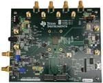
User's Guide
SLOU329B – November 2011 – Revised March 2015
AFE5807EVM (Rev E) Evaluation Module
This document assists users in evaluating the AFE5807 highly integrated analog front-end devices
through the use of the AFE5807EVM Evaluation Module. Included are setup instructions, printed-circuit
board art, bill of materials, and schematics.
Contents
Overview ...................................................................................................................... 2
Default Configuration ........................................................................................................ 3
Software Installation and Operation ....................................................................................... 4
Test Setup .................................................................................................................... 4
Power Up AFE5807 ......................................................................................................... 5
Launch AFE5807 GUI ....................................................................................................... 6
Launch TSW1400 GUI ...................................................................................................... 8
Test AFE5807 ................................................................................................................ 9
8.1
Step 1: Time Domain ............................................................................................... 9
8.2
Step 2: Single Tone FFT ......................................................................................... 12
9
Hardware Setup, CW Mode ............................................................................................... 13
9.1
Step 1: Switch to CW Mode. ..................................................................................... 14
9.2
Step 2: Apply input and observe outputs. ...................................................................... 15
9.3
External Clock for CW Mode..................................................................................... 16
10
External ADC Sampling Clock ............................................................................................ 18
11
External Vcntl ............................................................................................................... 20
12
Board Configuration ........................................................................................................ 21
12.1 Input/Output, Power Supply, and USB ......................................................................... 21
12.2 CW Mode, ADC Clock ............................................................................................ 22
12.3 Vcntl Control Input ................................................................................................ 23
12.4 LEDs ................................................................................................................ 24
12.5 Miscellaneous Test Points ....................................................................................... 25
13
EVM Printed-Circuit Board Layouts and Schematics .................................................................. 26
13.1 Schematics ......................................................................................................... 32
14
Bill of Materials ............................................................................................................. 41
Appendix A
High Speed Data Converter Pro GUI Installation (HSDCPro) ............................................... 45
1
2
3
4
5
6
7
8
List of Figures
1
AFE5807EVM Basic Configuration ........................................................................................ 3
2
HW Setup With Connection Between TSW1400EVM and AFE5807 ................................................. 4
3
User Interface: Single FFT Format ....................................................................................... 12
4
Setup for CW Mode ........................................................................................................ 13
5
Switching From Default (ADC) Mode Panel to CW Mode Panel..................................................... 14
6
CW Outputs ................................................................................................................. 15
7
Relevant Capacitors for CW Mode, Top Side .......................................................................... 16
8
Relevant Capacitors for CW Mode, Bottom Side ...................................................................... 17
9
External ADC Sampling Clock Configuration ........................................................................... 18
10
External Vcntl Configuration .............................................................................................. 20
11
I/O, PWR, and USB Connector ........................................................................................... 21
12
AFE5807EVM Jumper Locations......................................................................................... 22
SLOU329B – November 2011 – Revised March 2015
Submit Documentation Feedback
AFE5807EVM (Rev E) Evaluation Module
Copyright © 2011–2015, Texas Instruments Incorporated
1
�Overview
www.ti.com
13
Vcntl .......................................................................................................................... 23
14
AFE5807EVM LED Location .............................................................................................. 24
15
AFE5807EVM Test Point Locations ..................................................................................... 25
16
Top Layer - Signal.......................................................................................................... 26
17
Second Layer - Ground.................................................................................................... 27
18
Third Layer - Power ........................................................................................................ 28
19
......................................................................................................
.......................................................................................................
Bottom Layer - Signal ......................................................................................................
Schematic 1 of 9 ...........................................................................................................
Schematic 2 of 9 ...........................................................................................................
Schematic 3 of 9 ...........................................................................................................
Schematic 4 of 9 ...........................................................................................................
Schematic 5 of 9 ...........................................................................................................
Schematic 6 of 9 ...........................................................................................................
Schematic 7 of 9 ...........................................................................................................
Schematic 8 of 9 ...........................................................................................................
Schematic 9 of 9 ...........................................................................................................
HSDCPro Install (Begin)...................................................................................................
HSDCPro Install (Install Directory) .......................................................................................
HSDCPro Install (TI License Agreement) ...............................................................................
HSDCPro Install (NI License Agreement) ...............................................................................
HSDCPro Install (Start Installation) ......................................................................................
HSDCPro Install (Installation Progress) .................................................................................
HSDCPro Install (Installation Complete) ................................................................................
HSDCPro Install (h) ........................................................................................................
HSDCPro Install ............................................................................................................
20
21
22
23
24
25
26
27
28
29
30
31
32
33
34
35
36
37
38
39
Fourth Layer - Signal
Fifth Layer - Ground
29
30
31
32
33
34
35
36
37
38
39
40
45
46
47
48
49
50
51
52
52
List of Tables
1
1
Configuration for Clock Capacitors....................................................................................... 16
2
Input/Output, Power, and USB ........................................................................................... 21
....................................................................................................
3
CW Mode, ADC Clock
4
CW Mode and Vcntl ........................................................................................................ 23
5
LED Indicators .............................................................................................................. 24
6
Test Points .................................................................................................................. 25
7
Bill of Materials
.............................................................................................................
22
41
Overview
This document is intended to guide users step-by-step through the AFE5807EVM Evaluation Module
(EVM) setup and test . The EVM is shipped with a default configuration from the manufacturer. With this
configuration, the onboard CMOS clock is used for a analog-to-digital converter sampling clock; the
onboard oscillator is used for CW mode operation. No external clock generator is required. Users need to
provide the input signal for measurement from a signal generator.
Detail explanation regarding the jumpers, connectors, and test points appear in Section 12. The graphical
user interface (GUI) can be downloaded from the TI Web site.
2
AFE5807EVM (Rev E) Evaluation Module
SLOU329B – November 2011 – Revised March 2015
Submit Documentation Feedback
Copyright © 2011–2015, Texas Instruments Incorporated
�Default Configuration
www.ti.com
2
Default Configuration
Figure 1 shows the default configuration of the EVM from the factory. The accompanying list identifies the
basic components on the EVM board.
Figure 1. AFE5807EVM Basic Configuration
1.
2.
3.
4.
5.
6.
P1 – Power supplies connector.
JP1, JP2, and JP3 are set to enable 3.3-V, 1.8-V, and 5-V power supplies to device.
JP9: enables onboard CMOS clock.
JP10: Power supply for onboard CMOS clock oscillator.
JP15: Enables onboard VCNT.
JP31 always set as Figure 1.
SLOU329B – November 2011 – Revised March 2015
Submit Documentation Feedback
AFE5807EVM (Rev E) Evaluation Module
Copyright © 2011–2015, Texas Instruments Incorporated
3
�Software Installation and Operation
3
www.ti.com
Software Installation and Operation
The AFE5807EVM GUI (SLOC254) can be downloaded from the TI Web site. Follow the directions in
Read Me First.pdf file to install GUI and device driver
4
Test Setup
Two EVMs are required to evaluate the AFE5807 device. The following illustration shows the exact setup
of these two boards and external connectors. For the default configuration as shown in Figure 1, it is
unnecessary to have an external sampling clock and external Vcntl supply. The onboard CMOS clock and
onboard Vcntl are used.
Figure 2. HW Setup With Connection Between TSW1400EVM and AFE5807
4
AFE5807EVM (Rev E) Evaluation Module
SLOU329B – November 2011 – Revised March 2015
Submit Documentation Feedback
Copyright © 2011–2015, Texas Instruments Incorporated
�Power Up AFE5807
www.ti.com
5
Power Up AFE5807
Power up the AFE5807EVM by applying +5 V and –5 V to the P1 connector. After power up is complete,
four green LEDS and two red LEDS are turned on as shown in the following illustration.
LED 1.8V
SLOU329B – November 2011 – Revised March 2015
Submit Documentation Feedback
AFE5807EVM (Rev E) Evaluation Module
Copyright © 2011–2015, Texas Instruments Incorporated
5
�Launch AFE5807 GUI
6
www.ti.com
Launch AFE5807 GUI
Launch the AFE5807 graphic user interface (GUI), which appears in the following illustration. After the
GUI has completely launched, LED41 and LED42 go off and the rest of the LEDS remain on. The GUI
automatically configures the default setup. Select the ADC page to observe the default condition.
The following illustration shows the Default Condition on the ADC page.
6
AFE5807EVM (Rev E) Evaluation Module
SLOU329B – November 2011 – Revised March 2015
Submit Documentation Feedback
Copyright © 2011–2015, Texas Instruments Incorporated
�Launch AFE5807 GUI
www.ti.com
SLOU329B – November 2011 – Revised March 2015
Submit Documentation Feedback
AFE5807EVM (Rev E) Evaluation Module
Copyright © 2011–2015, Texas Instruments Incorporated
7
�Launch TSW1400 GUI
7
www.ti.com
Launch TSW1400 GUI
Launch the TSW1400 GUI. The Message window displays the following message to indicate that the
setup of the TSW1400EVM and AFE5807EVM is working properly. If a different message or an error
message appears, contact TI FAE.
Also see Appendix Afor how to download the software.
Select AFE5807, 12 bits, MSB first from the GUI.
ADC Sampling Rate is fixed at 40 MHz; this is the onboard CMOS clock frequency.
ADC Input Frequency – enter 2M, and the GUI calculates the real coherent frequency to 2.00439453M.
8
AFE5807EVM (Rev E) Evaluation Module
SLOU329B – November 2011 – Revised March 2015
Submit Documentation Feedback
Copyright © 2011–2015, Texas Instruments Incorporated
�Test AFE5807
www.ti.com
8
Test AFE5807
8.1
Step 1: Time Domain
•
Select the Time Domain page from the TSW1400 GUI.
SLOU329B – November 2011 – Revised March 2015
Submit Documentation Feedback
AFE5807EVM (Rev E) Evaluation Module
Copyright © 2011–2015, Texas Instruments Incorporated
9
�Test AFE5807
•
From the AFE5807 GUI, go to the ADC page, and then select Ramp.
•
Press the Capture button on the TSW1400 GUI. This displays a ramping waveform on the TSW1400
GUI display area as shown in the following illustration.
Repeat for Channel 2 and Channel 8.
If each channel has the output as shown in the following illustration, proceed with the next
step; otherwise, contact the TI FAE to troubleshoot the problem.
On the AFE5807 GUI, change Test Pattern from Ramp to None for the next step.
•
•
•
10
www.ti.com
AFE5807EVM (Rev E) Evaluation Module
SLOU329B – November 2011 – Revised March 2015
Submit Documentation Feedback
Copyright © 2011–2015, Texas Instruments Incorporated
�Test AFE5807
www.ti.com
SLOU329B – November 2011 – Revised March 2015
Submit Documentation Feedback
AFE5807EVM (Rev E) Evaluation Module
Copyright © 2011–2015, Texas Instruments Incorporated
11
�Test AFE5807
8.2
www.ti.com
Step 2: Single Tone FFT
•
•
•
•
•
•
•
Select the Single Tone FFT page at the TSW1400 GUI.
Connect Channel 1 of the AFE5807EVM to a signal generator through an LP filter. If an LP filter is not
present, the result will not be good.
Set the amplitude of the signal generator to -25dBm.
Set the frequency of the signal generator to 1.99645996M to match the GUI.
Change the window option to Hanning. This is because the input signal and the onboard CMOS clock
are noncoherent.
Press the Capture button to get the test result.
Repeat for Channel 2 through Channel 8.
Figure 3. User Interface: Single FFT Format
12
AFE5807EVM (Rev E) Evaluation Module
SLOU329B – November 2011 – Revised March 2015
Submit Documentation Feedback
Copyright © 2011–2015, Texas Instruments Incorporated
�Hardware Setup, CW Mode
www.ti.com
9
Hardware Setup, CW Mode
Figure 4. Setup for CW Mode
SLOU329B – November 2011 – Revised March 2015
Submit Documentation Feedback
AFE5807EVM (Rev E) Evaluation Module
Copyright © 2011–2015, Texas Instruments Incorporated
13
�Hardware Setup, CW Mode
9.1
www.ti.com
Step 1: Switch to CW Mode.
•
•
•
Go to the CW Mode page.
Check CW Mode Enable. The LED41, LED42, and LED43 on AFE5807EVM all illuminate.
Select 500 Ω for the gain control feedback resistor.
Figure 5. Switching From Default (ADC) Mode Panel to CW Mode Panel
14
AFE5807EVM (Rev E) Evaluation Module
SLOU329B – November 2011 – Revised March 2015
Submit Documentation Feedback
Copyright © 2011–2015, Texas Instruments Incorporated
�Hardware Setup, CW Mode
www.ti.com
9.2
Step 2: Apply input and observe outputs.
•
•
Apply an analog signal (2.51 M, –10 dBm) to any analog input SMA.
The CW outputs (J12, J13) display the frequency I and Q signals at 10 kHz as shown in Figure 6. The
GUI Gain Control Feedback Resistor can be used to vary the amplitude of the outputs.
Figure 6. CW Outputs
SLOU329B – November 2011 – Revised March 2015
Submit Documentation Feedback
AFE5807EVM (Rev E) Evaluation Module
Copyright © 2011–2015, Texas Instruments Incorporated
15
�Hardware Setup, CW Mode
9.3
www.ti.com
External Clock for CW Mode
The CW mode clocks can be supplied from J9 (X16/X8/X4/X1) and J10 (X1) using external signal
generators. The manufacture default setup uses ON BOARD CLOCK, with which C154, C155, C156, and
C157 are installed. To switch to an external clock, these four capacitors must be uninstalled and
capacitors C49,C50,C52, and C53 must be installed. The following table shows the configuration for these
eight capacitors.
Table 1. Configuration for Clock Capacitors
Capacitor
Onboard Clock
External Clock
Comments
C49
Uninstalled
Installed
Top layer of the EVM
C50
Uninstalled
Installed
Bottom layer of the EVM
C52
Uninstalled
Installed
Bottom layer of the EVM
C53
Uninstalled
Installed
Top layer of the EVM
C154
Installed
Uninstalled
Top layer of the EVM
C155
Installed
Uninstalled
Top layer of the EVM
C156
Installed
Uninstalled
Top layer of the EVM
C157
Installed
Uninstalled
Top layer of the EVM
C49
C154
C155
C156
C157
C53
Figure 7. Relevant Capacitors for CW Mode, Top Side
16
AFE5807EVM (Rev E) Evaluation Module
SLOU329B – November 2011 – Revised March 2015
Submit Documentation Feedback
Copyright © 2011–2015, Texas Instruments Incorporated
�Hardware Setup, CW Mode
www.ti.com
C50
C52
Figure 8. Relevant Capacitors for CW Mode, Bottom Side
SLOU329B – November 2011 – Revised March 2015
Submit Documentation Feedback
AFE5807EVM (Rev E) Evaluation Module
Copyright © 2011–2015, Texas Instruments Incorporated
17
�External ADC Sampling Clock
10
www.ti.com
External ADC Sampling Clock
To
1.
2.
3.
use the external clock generator to test the AFE5807, perform the following steps.
Reconfigure JP9 as shown in the following illustration. The rest of the jumpers remain the same.
Connect the external generator as shown in Figure 9.
Set the generator output to 40 MHz, 13 dBm.
Figure 9. External ADC Sampling Clock Configuration
18
AFE5807EVM (Rev E) Evaluation Module
SLOU329B – November 2011 – Revised March 2015
Submit Documentation Feedback
Copyright © 2011–2015, Texas Instruments Incorporated
�External ADC Sampling Clock
www.ti.com
4. If the generators for the ADC clock and input signal are synchronous, then choose Rectangular as the
Windowing option; otherwise, use Hanning or Hamming.
5. The test procedure is the same for the CMOS ADC clock.
SLOU329B – November 2011 – Revised March 2015
Submit Documentation Feedback
AFE5807EVM (Rev E) Evaluation Module
Copyright © 2011–2015, Texas Instruments Incorporated
19
�External Vcntl
11
www.ti.com
External Vcntl
•
•
JP15 needs to be reconfigured to short the leftmost two pins.
A power supply is required to be connected as shown in Figure 10.
Figure 10. External Vcntl Configuration
20
AFE5807EVM (Rev E) Evaluation Module
SLOU329B – November 2011 – Revised March 2015
Submit Documentation Feedback
Copyrigh