User's Guide
SLOU309 – December 2010
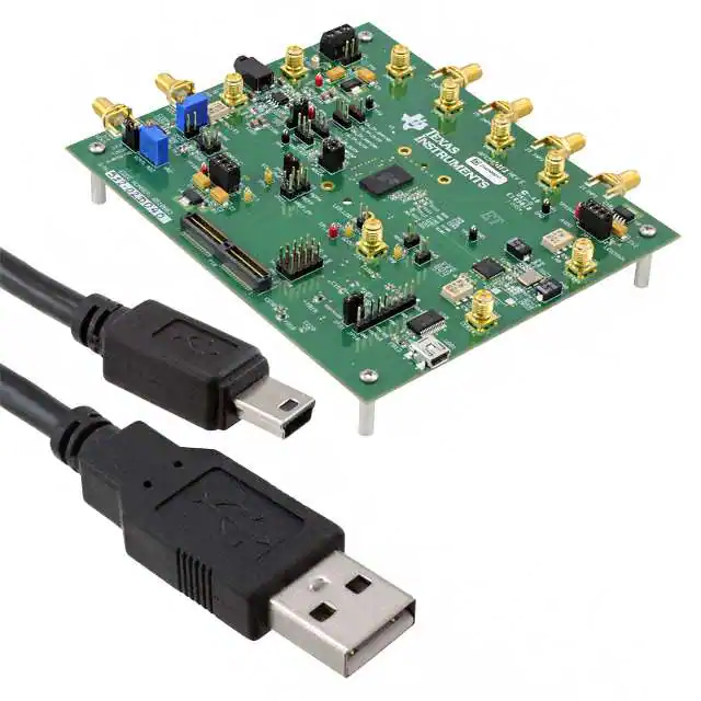
AFE5807/08EVM (Rev D) Evaluation Module
This document assists users in evaluating the AFE5807 and AFE5808 highly integrated analog front-end
devices through the use of the AFE5807/08EVM Evaluation Module. Included are setup instructions,
printed-circuit board art, bill of materials, and schematics.
13
14
Contents
Overview ..................................................................................................................... 2
Default Configuration ....................................................................................................... 2
Software Installation and Operation ...................................................................................... 3
3.1
GUI Installation (Mandatory) ...................................................................................... 3
3.2
USB Interface Driver Installation ................................................................................. 3
Test Setup ................................................................................................................... 5
Power Up AFE5807/08 ..................................................................................................... 6
Launch AFE5807/08 GUI .................................................................................................. 6
Launch TSW1250 GUI ..................................................................................................... 7
TEST AFE5807/08 .......................................................................................................... 8
8.1
Step 1: Time Domain .............................................................................................. 8
8.2
Step 2: Single Tone FFT ........................................................................................ 10
Hardware Setup, CW Mode .............................................................................................. 12
9.1
Step 1: Switch to CW Mode. .................................................................................... 12
9.2
Step 2: Apply input and observe outputs. ..................................................................... 13
9.3
External Clock for CW Mode .................................................................................... 14
External ADC Sampling Clock ........................................................................................... 16
External Vcntl .............................................................................................................. 18
Board Configuration ....................................................................................................... 20
12.1 Input/Output, Power Supply, and USB ........................................................................ 20
12.2 CW Mode, ADC Clock ........................................................................................... 21
12.3 Vcntl Control Input ................................................................................................ 22
12.4 LEDs ............................................................................................................... 23
12.5 Miscellaneous Test Points ....................................................................................... 24
EVM Printed-Circuit Board Layouts and Schematics ................................................................. 25
Bill of Materials ............................................................................................................. 31
1
AFE5807/08EVM Basic Configuration
1
2
3
4
5
6
7
8
9
10
11
12
List of Figures
2
3
4
5
6
7
8
9
10
11
................................................................................... 3
HW Setup With Connection Between TSW1250EVM and AFE5807/08 ............................................ 5
User Interface: Single FFT Format ...................................................................................... 11
Setup for CW Mode ....................................................................................................... 12
Switching From Default (ADC) Mode Panel to CW Mode Panel .................................................... 13
CW Outputs ................................................................................................................ 14
Relevant Capacitors for CW Mode, Top Side ......................................................................... 15
Relevant Capacitors for CW Mode, Bottom Side ..................................................................... 16
External ADC Sampling Clock Configuration .......................................................................... 17
External Vcntl Configuration ............................................................................................. 19
I/O, PWR, and USB Connector .......................................................................................... 20
Windows is a trademark of Microsoft Corporation.
SLOU309 – December 2010
Submit Documentation Feedback
AFE5807/08EVM (Rev D) Evaluation Module
Copyright © 2010, Texas Instruments Incorporated
1
�Overview
www.ti.com
12
AFE5807/08EVM Jumper Locations .................................................................................... 21
13
Vcntl ......................................................................................................................... 22
14
AFE5807/08EVM LED Location ......................................................................................... 23
15
AFE5807/08EVM Test Point Locations ................................................................................. 24
16
Top Layer - Signal ......................................................................................................... 25
17
Second Layer - Ground ................................................................................................... 26
18
Third Layer - Power ....................................................................................................... 27
19
Fourth Layer - Signal...................................................................................................... 28
20
Fifth Layer - Ground ....................................................................................................... 29
21
Bottom Layer - Signal ..................................................................................................... 30
List of Tables
1
Configuration for Clock Capacitors ...................................................................................... 14
2
Input/Output, Power, and USB
20
3
CW Mode, ADC Clock
21
4
5
6
7
1
..........................................................................................
...................................................................................................
CW Mode and Vcntl .......................................................................................................
LED Indicators .............................................................................................................
Test Points .................................................................................................................
Bill of Materials.............................................................................................................
22
23
24
31
Overview
This document is intended to guide users step-by-step through the AFE5807/08EVM Evaluation Module
(EVM) setup and test . The EVM is shipped with a default configuration from the manufacturer. With this
configuration, the onboard CMOS clock is used for a analog-to-digital converter sampling clock; the
onboard oscillator is used for CW mode operation. No external clock generator is required. Users need to
provide the input signal for measurement from a signal generator.
Detail explanation regarding the jumpers, connectors, and test points appear in Section 12. The graphical
user interface (GUI) can be downloaded from the TI Web site.
2
Default Configuration
Figure 1 shows the default configuration of the EVM from the factory. The accompanying list identifies the
basic components on the EVM board.
2
AFE5807/08EVM (Rev D) Evaluation Module
Copyright © 2010, Texas Instruments Incorporated
SLOU309 – December 2010
Submit Documentation Feedback
�Software Installation and Operation
www.ti.com
JP1
+5V
JP2
GND
-5V
JP 9
JP3
JP10
JP1
JP15
JP31
Figure 1. AFE5807/08EVM Basic Configuration
1.
2.
3.
4.
5.
6.
3
P1 – Power supplies connector.
JP1, JP2, and JP3 are set to enable 3.3-V, 1.8-V, and 5-V power supplies to device.
JP9: enables onboard CMOS clock.
JP10: Power supply for onboard CMOS clock oscillator.
JP15: Enables onboard VCNT.
JP31 always set as Figure 1.
Software Installation and Operation
The AFE5807/08EVM comes with a software installation compact disk (CD); run setup.exe to install the
software.
3.1
GUI Installation (Mandatory)
Unzip the installer file in the CD. Run setup.exe to install the GUI.
3.2
USB Interface Driver Installation
•
•
Connect the USB port of the EVM to your personal computer (PC).
If the driver has not been installed, then the message "Window Found New Hardware" appears. As
shown in the following illustration, the Wizard launches. Otherwise, skip this section, and go to
Section 4.
SLOU309 – December 2010
Submit Documentation Feedback
AFE5807/08EVM (Rev D) Evaluation Module
Copyright © 2010, Texas Instruments Incorporated
3
�Software Installation and Operation
•
Select "No, not this time" from the options. Press the Next button.
•
Select "Install from a list or specific location (Advanced)" as shown in the following illustration, and then
click "Next."
•
Select "Search for the best driver in these locations," and enter the file path C:\Program Files\Texas
Instruments\CDM 2.04.06 WHQL Certified in the combo-box, or browse to it by clicking the browse
button. Once the file path has been entered in the box, click Next to proceed.
If Windows™ XP is configured to warn when unsigned (non-WHQL certified) drivers are about to be
installed, the following screen is displayed unless installing a Microsoft WHQL certified driver. Click on
"Continue Anyway" to continue with the installation. If Windows XP is configured to ignore file signature
warnings, no message appears.
•
4
www.ti.com
AFE5807/08EVM (Rev D) Evaluation Module
Copyright © 2010, Texas Instruments Incorporated
SLOU309 – December 2010
Submit Documentation Feedback
�Test Setup
www.ti.com
4
Test Setup
Two EVMs are required to evaluate the AFE5807/08 device. The following illustration shows the exact
setup of these two boards and external connectors. For the default configuration as shown in Figure 1, it is
unnecessary to have an external sampling clock and external Vcntl supply. The onboard CMOS clock and
onboard Vcntl are used.
Ground
USB Interface
USB Interface
Filter for input signal
-5 V PowerSupply
+5 V PowerSupply
+6V supply
ADC (external) sampling
Vcntl Supply;
-
Figure 2. HW Setup With Connection Between TSW1250EVM and AFE5807/08
SLOU309 – December 2010
Submit Documentation Feedback
AFE5807/08EVM (Rev D) Evaluation Module
Copyright © 2010, Texas Instruments Incorporated
5
�Power Up AFE5807/08
5
www.ti.com
Power Up AFE5807/08
Power up the AFE5807/08EVM by applying +5 V and –5 V to the P1 connector. After power up is
complete, four green LEDS and two red LEDS are turned on as shown in the following illustration.
P1
LED3.3VA
LED- 5V
LED3.3VD
LED5V
LED41
LED42
LED1.8V
6
Launch AFE5807/08 GUI
Launch the AFE5807/08 graphic user interface (GUI), which appears in the following illustration. After the
GUI has completely launched, LED41 and LED42 go off and the rest of the LEDS remain on. The GUI
automatically configures the default setup. Select the ADC page to observe the default condition.
6
AFE5807/08EVM (Rev D) Evaluation Module
Copyright © 2010, Texas Instruments Incorporated
SLOU309 – December 2010
Submit Documentation Feedback
�Launch TSW1250 GUI
www.ti.com
The following illustration shows the Default Condition on the ADC page.
7
Launch TSW1250 GUI
Launch the TSW1250 GUI. The Message window displays the following message to indicate that the
setup of the TSW1250EVM and AFE5807/08EVM is working properly. If a different message or an error
message appears, contact TI FAE.
Select AFE5807, 14 bits, MSB first from the GUI.
SLOU309 – December 2010
Submit Documentation Feedback
AFE5807/08EVM (Rev D) Evaluation Module
Copyright © 2010, Texas Instruments Incorporated
7
�TEST AFE5807/08
www.ti.com
ADC Sampling Rate is fixed at 40 MHz; this is the onboard CMOS clock frequency.
ADC Input Frequency – enter 2M, and the GUI calculates the real coherent frequency to 2.00439453M.
Select
ADC Sampling
Rate
ADC Input
Frequency
Message
8
TEST AFE5807/08
8.1
Step 1: Time Domain
•
•
8
Select the Time Domain page from the TSW1250 GUI.
Uncheck Overlay unwrap waveform.
AFE5807/08EVM (Rev D) Evaluation Module
Copyright © 2010, Texas Instruments Incorporated
SLOU309 – December 2010
Submit Documentation Feedback
�TEST AFE5807/08
www.ti.com
Overlay unwrap waveform
•
From the AFE5808 GUI, go to the ADC page, and then select Ramp.
•
Press the Capture button on the TSW1250 GUI. You will observe a ramping waveform on the
TSW1250 GUI display area as shown in the following illustration.
Repeat for Channel 2 and Channel 8.
•
SLOU309 – December 2010
Submit Documentation Feedback
AFE5807/08EVM (Rev D) Evaluation Module
Copyright © 2010, Texas Instruments Incorporated
9
�TEST AFE5807/08
•
•
8.2
If each channel has the output as shown in the following illustration, proceed with the next
step; otherwise, contact the TI FAE to troubleshoot the problem.
On the AFE5808 GUI, change Test Pattern from Ramp to None for the next step.
Step 2: Single Tone FFT
•
•
•
•
•
•
•
10
www.ti.com
Select the Single Tone FFT page at the TSW1250 GUI.
Connect Channel 1 of the AFE5807EVM to a signal generator through an LP filter. If an LP filter is not
present, the result will not be good.
Set the amplitude of the signal generator to -25dBm.
Set the frequency of the signal generator to 2.00439453M to match the GUI.
Change the window option to Hanning. This is because the input signal and the onboard CMOS clock
are noncoherent.
Press the Capture button to get the test result.
Repeat for Channel 2 through Channel 8.
AFE5807/08EVM (Rev D) Evaluation Module
Copyright © 2010, Texas Instruments Incorporated
SLOU309 – December 2010
Submit Documentation Feedback
�TEST AFE5807/08
www.ti.com
Hanning
Figure 3. User Interface: Single FFT Format
SLOU309 – December 2010
Submit Documentation Feedback
AFE5807/08EVM (Rev D) Evaluation Module
Copyright © 2010, Texas Instruments Incorporated
11
�Hardware Setup, CW Mode
9
www.ti.com
Hardware Setup, CW Mode
Note that LEDs
41- 43 are on
CW outputs (I
and Q) (J12, 13)
Analog input
(note absence
of filter) (J1 - J8)
Figure 4. Setup for CW Mode
9.1
Step 1: Switch to CW Mode.
•
•
•
12
Go to the CW Mode page.
Check CW Mode Enable. The LED41, LED42, and LED43 on AFE5807/08EVM all illuminate.
Select 500ohms for the gain control feedback resistor.
AFE5807/08EVM (Rev D) Evaluation Module
Copyright © 2010, Texas Instruments Incorporated
SLOU309 – December 2010
Submit Documentation Feedback
�Hardware Setup, CW Mode
www.ti.com
CW Mode Enabled
500 W
Gain Control
Feedback Resistor
Figure 5. Switching From Default (ADC) Mode Panel to CW Mode Panel
9.2
Step 2: Apply input and observe outputs.
•
•
Apply an analog signal (2.51 M, –10 dBm) to any analog input SMA.
The CW outputs (J12, J13) display the frequency I and Q signals at 10 kHz as shown in Figure 6. The
GUI Gain Control Feedback Resistor can be used to vary the amplitude of the outputs.
SLOU309 – December 2010
Submit Documentation Feedback
AFE5807/08EVM (Rev D) Evaluation Module
Copyright © 2010, Texas Instruments Incorporated
13
�Hardware Setup, CW Mode
www.ti.com
Figure 6. CW Outputs
9.3
External Clock for CW Mode
The CW mode clocks can be supplied from J9 (X16/X8/X4/X1) and J10 (X1) using external signal
generators. The manufacture default setup uses ON BOARD CLOCK, with which C154, C155, C156, and
C157 are installed. To switch to an external clock, these four capacitors must be uninstalled and
capacitors C49,C50,C52, and C53 must be installed. The following table shows the configuration for these
eight capacitors.
Table 1. Configuration for Clock Capacitors
14
Capacitor
Onboard Clock
External Clock
C49
Uninstalled
Installed
Top layer of the EVM
C50
Uninstalled
Installed
Bottom layer of the EVM
C52
Uninstalled
Installed
Bottom layer of the EVM
C53
Uninstalled
Installed
Top layer of the EVM
C154
Installed
Uninstalled
Top layer of the EVM
C155
Installed
Uninstalled
Top layer of the EVM
C156
Installed
Uninstalled
Top layer of the EVM
C157
Installed
Uninstalled
Top layer of the EVM
AFE5807/08EVM (Rev D) Evaluation Module
Copyright © 2010, Texas Instruments Incorporated
Comments
SLOU309 – December 2010
Submit Documentation Feedback
�Hardware Setup, CW Mode
www.ti.com
C49
C154
C155
C156
C157
C53
Figure 7. Relevant Capacitors for CW Mode, Top Side
SLOU309 – December 2010
Submit Documentation Feedback
AFE5807/08EVM (Rev D) Evaluation Module
Copyright © 2010, Texas Instruments Incorporated
15
�External ADC Sampling Clock
www.ti.com
C50
C52
Figure 8. Relevant Capacitors for CW Mode, Bottom Side
10
External ADC Sampling Clock
To
1.
2.
3.
16
use the external clock generator to test the AFE5807/08, perform the following steps.
Reconfigure JP9 as shown in the following illustration. The rest of the jumpers remain the same.
Connect the external generator as shown in Figure 9.
Set the generator output to 40 MHz, 13 dBm.
AFE5807/08EVM (Rev D) Evaluation Module
Copyright © 2010, Texas Instruments Incorporated
SLOU309 – December 2010
Submit Documentation Feedback
�External ADC Sampling Clock
www.ti.com
JP9
Ext Clock
Connector
Figure 9. External ADC Sampling Clock Configuration
4. If the generators for the ADC clock and input signal are synchronous, then choose Rectangular as the
Windowing option; otherwise, use Hanning or Hamming.
SLOU309 – December 2010
Submit Documentation Feedback
AFE5807/08EVM (Rev D) Evaluation Module
Copyright © 2010, Texas Instruments Incorporated
17
�External Vcntl
www.ti.com
5. The test procedure is the same for the CMOS ADC clock.
11
External Vcntl
•
•
18
JP15 needs to be reconfigured to short the leftmost two pins.
A power supply is required to be connected as shown in Figure 10.
AFE5807/08EVM (Rev D) Evaluation Module
Copyright © 2010, Texas Instruments Incorporated
SLOU309 – December 2010
Submit Documentation Feedback
�External Vcntl
www.ti.com
Power
Supply
JP15
Figure 10. External Vcntl Configuration
SLOU309 – December 2010
Submit Documentation Feedback
AFE5807/08EVM (Rev D) Evaluation Module
Copyright © 2010, Texas Instruments Incorporated
19
�Board Configuration
12
www.ti.com
Board Configuration
12.1 Input/Output, Power Supply, and USB
J7
P1
J5
J8
JP6
J6
J3
J4
J1
J2
JP2
TP33VA
TP1
TP3
TP -5V
TP33VD
TP5V
TP2
JP3
TP4
JP1
USB1
TP18VD
JP18
Figure 11. I/O, PWR, and USB Connector
Table 2. Input/Output, Power, and USB
20
Connector
Description
J1 through J8
Analog Input signals for Ch1 through Ch8. Connect to a signal generator. A bandpass filter must be applied
between the generator and the SMA to get a better result. (See Figure 1 .)
P1/JP6
P1 is the +5-V and –5-V power supply connector. JP6 is the test point for +5-V/-5-V power supply.
JP3
Onboard 5-V enable. Set up as Figure 2 is a must to use onboard 5-V supply.
XP-5V
-5-V supply test point.
TP5V
+5-V supply test point.
JP1
Onboard +1.8-V enable. Set up as shown in Figure 2; required to use the onboard +1.8 V.
JP2
Onboard 3.3-VA enable. Set up as shown in Figure 2; required to use the onboard 3.3 V.
TP18VD
+1.8-VD supply test point.
TP33VD
+3.3-VD supply test point.
TP33VA
+3.3-VA supply test point.
TP1 through TP4
Ground test points.
USB1
USB interface connector
JP18
Test points for USB data bus: From pin 1 to pin 9 the signals are: D0, D4, D2, D1, D7, D5, D6, and D3
AFE5807/08EVM (Rev D) Evaluation Module
Copyright © 2010, Texas Instruments Incorporated
SLOU309 – December 2010
Submit Documentation Feedback
�Board Configuration
www.ti.com
12.2 CW Mode, ADC Clock
CW_IP_OUTP / CW_IP_OUTM
JP52
PGA output to CW input (CH7)
J9
J12
JP53
JP57
PGA output to CW input (CH8)
JX1
JP56
J13
JP9
CW_IP_OUTP / CW_IP_OUTM
JP10
J14
J10
Figure 12. AFE5807/08EVM Jumper Locations
Table 3. CW Mode, ADC Clock
Clock
Type
Reference
Designator
Description
J9/J10
External CW Mode clock. The default is using onboard oscillator.
J12
JP52/JP53
CW Mode
J13
JP56/JP57
ADC
CW output for I-channel via an external operational amplifier. The EVM has converted the
differential signal CW_IP_OUTP and CW_IP_OUTM into this single-ended output through an
operational amplifier.
To observe CW_IP_OUTP and CW_IP_OUTM before the external operational amplifier, the user
can probe JP52 and JP53.
CW output for V-channel via an external operational amplifier. The EVM has converted the
differential signal CW_VP_OUTP and CW_VP_OUTM into this single-ended output through an
operational amplifier.
To observe CW_VP_OUTP and CW_VP_OUTM before the external operational amplifier, the user
can probe JP56 and JP57.
JX1
This connector allows the user to see signals of J12 and J13 simultaneously.
JP9/JP10
JP9 selects on_board_ADC CMOS clock or external clock from J14. Default setup in Figure 4 uses
onboard CMOS clock. Set it to the other side to use the external clock source.
Short to power up onboard CMOS clock.
J14
SLOU309 – December 2010
Submit Documentation Feedback
External ADC clock Input.
AFE5807/08EVM (Rev D) Evaluation Module
Copyright © 2010, Texas Instruments Incorporated
21
�Board Configuration
www.ti.com
12.3 Vcntl Control Input
J14
JP15
Figure 13. Vcntl
Table 4. CW Mode and Vcntl
22
Connector
Description
JP15
Choose onboard Vcntl or external Vcntl. The default setup uses onboard Vcntl.
J14
External Vcntl input. The range is from 0 V to 1.5 V.
VR2
Onboard Vcntl adjustment. Use JP15 pin 3 which has the text On-Board to monitor the Vcntl voltage level.
AFE5807/08EVM (Rev D) Evaluation Module
Copyright © 2010, Texas Instruments Incorporated
SLOU309 – December 2010
Submit Documentation Feedback
�Board Configuration
www.ti.com
12.4 LEDs
The AFE5807/08EVM has seven LEDs. Their locations are shown in Figure 14. Their ON/OFF states
demonstrate the normal operation of the power supplies and the PLL status of the clock buffer.
LED3.3VA
LED - 5V
LED3.3VD
LED5V
LED41
LED42
LED1.8VA
Figure 14. AFE5807/08EVM LED Location
Table 5. LED Indicators
Reference Designator
Power Supply
Color
LED-5V
–5 V
Green
LED5V
+5 V
Green
LED3.3VD
+3.3 VD
Orange
LED3.3VA
+3.3 VA
Green
LED1.8V
+1.8 VV
Green
LED41
LED42
SLOU309 – December 2010
Submit Documentation Feedback
Clock Buffer Status Indicator
Red
Red
AFE5807/08EVM (Rev D) Evaluation Module
Copyright © 2010, Texas Instruments Incorporated
23
�Board Configuration
www.ti.com
12.5 Miscellaneous Test Points
TP44
JP19
TP45
TP9
JP20
TP12
JP21
TP13
Figure 15. AFE5807/08EVM Test Point Locations
Table 6. Test Points
24
Reference Designator
Description
TP9, TP12, TP13,TP34
AFE5807/08 device test pin M8, L5, M5, and M9
JP19
REFM voltage input
JP31
SDOUT read enable
JP44
RESET input. Short to reset AFE5807.
JP45
TP_5 control enable
JP20
REFP voltage input
JP21
REF_IN voltage input
AFE5807/08EVM (Rev D) Evaluation Module
Copyright © 2010, Texas Instruments Incorporated
SLOU309 – December 2010
Submit Documentation Feedback
�www.ti.com
13
EVM Printed-Circuit Board Layouts and Schematics
EVM Printed-Circuit Board Layouts and Schematics
The following illustrations show the six layers of the AFE5807/08EVM board.
Figure 16. Top Layer - Signal
SLOU309 – December 2010
Submit Documentation Feedback
AFE5807/08EVM (Rev D) Evaluation Module
Copyright © 2010, Texas Instruments Incorporated
25
�EVM Printed-Circuit Board Layouts and Schematics
www.ti.com
Figure 17. Second Layer - Ground
26
AFE5807/08EVM (Rev D) Evaluation Module
Copyright © 2010, Texas Instruments Incorporated
SLOU309 – December 2010
Submit Documentation Feedback
�www.ti.com
EVM Printed-Circuit Board Layouts and Schematics
Figure 18. Third Layer - Power
SLOU309 – December 2010
Submit Documentation Feedback
AFE5807/08EVM (Rev D) Evaluation Module
Copyright © 2010, Texas Instruments Incorporated
27
�EVM Printed-Circuit Board Layouts and Schematics
www.ti.com
Figure 19. Fourth Layer - Signal
28
AFE5807/08EVM (Rev D) Evaluation Module
Copyright © 2010, Texas Instruments Incorporated
SLOU309 – December 2010
Submit Documentation Feedback
�EVM Printed-Circuit Board Layouts and Schematics
www.ti.com
+
+
+
+
Figure 20. Fifth Layer - Ground
SLOU309 – December 2010
Submit Documentation Feedback
AFE5807/08EVM (Rev D) Evaluation Module
Copyright © 2010, Texas Instruments Incorporated
29
�EVM Printed-Circuit Board Layouts and Schematics
www.ti.com
+
+
+
+
7 1 2 0 0 1 - L-S LI
Figure 21. Bottom Layer - Signal
The schematic sheets are appended to the end of this document.
30
AFE5807/08EVM (Rev D) Evaluation Module
Copyright © 2010, Texas Instruments Incorporated
SLOU309 – December 2010
Submit Documentation Feedback
�Bill of Materials
www.ti.com
14
Bill of Materials
Table 7. Bill of Materials
QTY
MFG
MFG PART No.
REF DES
DESCRIPTION
VALUE OR FUNCTION
89
AVX
0402YC104KAT2A
C21, C22, C23, C24, C25,
C26, C27, C28, C29, C30,
C31, C32, C33, C34, C35,
C36, C37, C48, C49, C50,
C51, C52, C53, C54, C59,
C64, C71, C72, C73, C74,
C75, C76, C77, C78, C79,
C80, C81, C82, C83, C84,
C85, C90, C95, C96, C97,
C98, C99, C100, C101,
C102,
CAP,SMT,0402
CAPACITOR, SMT ,0402, CER, 16V, 10%, 0.1uF
C103,
C107,
C115,
C119,
C124,
C132,
C153,
C157,
C183,
C228,
C104,
C108,
C116,
C120,
C125,
C150,
C154,
C159,
C191,
C229,
C105,
C109,
C117,
C122,
C126,
C151,
C155,
C161,
C226,
C230
C106,
C112,
C118,
C123,
C130,
C152,
C156,
C182,
C227,
DO NOT INSTALL C49, C50, C116, C117, C52, C53
4
AVX
0402YC332KAT2A
C192, C193, C223, C224
CAP,SMT,0402
CAPACITOR, SMT, 0402, CER, 16V, 10%, 3300pF
9
KEMET
C0402C104K8PAC
C2, C3, C6, C7, C10, C11,
C14, C18, C56
CAP,SMT,0402
CAPACITOR, SMT, 0402, CER, 0.1uF, 10V, 10%, X5R
4
ANY
C0402_PAD020X020_0
40LS(UN)
C113, C114, C231, C232
CAP,SMT,0402
CAP,0402, ALTERNAT FOOTPRINT, PAD 020x020, 040LS
(Uninstalled Part)
8
PANASONIC
ECJ-0EB1C153K
C38, C39, C40, C41, C42,
C43, C44, C45
CAP,SMT,0402
CAPACITOR, SMT, 0402, CERAMIC, 0.015uF, 16V, 10%,
X7R
1
PANASONIC
ECJ-0EB1H102K
C175
CAP,SMT,0402
CAPACITOR, SMT, 0402, CER, 1000pF, 50V, 10%, X7R
4
PANASONIC
ECJ-0EB1H332K
C140, C141, C148, C149
CAP,SMT,0402
CAPACITOR, SMT, 0402, CER, 3300pF, 50V, 10%, X7R
2
PANASONIC
ECJ-0EC1H470J
C146, C147
CAP,SMT,0402
CAPACITOR, SMT, 0402, CER, 47pF, 50V, 5%, NPO
2
TAIYO YUDEN
LMK105F104ZV
C92, C93
CAP,SMT,0402
CAPACITOR, SMT, 0402, CERAMIC, 10V, Y5V, 0.1uF, 20%
DO NOT INSTALL
2
PANASONIC
ECJ-0EB1A105M
C110, C111
CAP,SMT,0402
CAPACITOR, SMT, 0402, CERAMIC, 1.0uF, 10V, 20%, X5R
5
AVX
0603YD105KAT2A
C121, C129, C131, C158,
C160
CAP,SMT,0603
CAPACITOR, SMT, 0603, CERAMIC, 1.0uF, 16V, 10%, X5R
4
PANASONIC
ECJ-1VB1C105K
C20, C70, C87, C89
CAP,SMT,0603
CAPACITOR, SMT, 0603, CERAMIC, 1.0uF, 16V, 10%, X5R
1
TAIYO YUDEN
JMK107BJ106MA-T
C176
CAP,SMT,0603
CAPACITOR, SMT, 0603, CERAMIC, 10uF, 6.3V, 20%,X5R
6
KEMET
C1206C226K8PAC
C61, C62, C163, C164,
C165, C166
CAP,SMT,1206
CAPACITOR, SMT, 1206, CERAMIC, 22uF, 10V, 10%, X5R
5
VISHAY SPRAGE
293D226X9016D2T
C19, C69, C86, C88, C91
CAP,SMT,7343
CAP, TAN, SMT, 22uF, 16V, +/-10%, -55~85C DO NOT
INSTALL C91
8
AVX
TPSC226K016R0375
C1, C4, C5, C8, C9, C12,
C13, C17
CAPACITOR, SMT, TANT
10%, 16V, 22uF
1
ADVANCED
CONNECTEK
MNE20-5K5P10
USB1
CONN,SMT,5P
MINI-AB USB OTG RECEPTACLE R/A SMT TYPE
6
EF JOHNSON
142-0721-891
J1, J3, J5, J7, J14, J15
CONN, THU, SMA JACK
SMA JACK END LAUNCH, 0.080 PCB THICK
9
AMPHENOL
901-144-8
J2, J4, J6, J8, J9, J10, J11,
J12, J13
CONNECTOR, SMA
SMA COAX STRAIGHT PCB CURRENT P/N IS
901-144-8RFX
1
*YOKOWO
SEMICONDUCTO
R TEST
SB5549-0000-E-1(SP)
U1
CUSTOMER PROVIDE
HTSOCKET, SMT, 135P, BGA, 1mmLS, 022PAD
(CUSTOMER PROVIDE)
1
INFINEON
BAT68-04(UN)
D1
DIODE,SMT,SOT23-3
SILICON SCHOTTKY DIODES, SMT, SOT23-3, DUAL, 8V,
130mA, 150mW (UNI)
1
MURATA
BLM15BD102SN1D
FB16
FERRITE BEAD,SMT,0402
FERRITE BEAD, SMT, 0402, 1K OHM, 200mA
16
STEWARD
HI0805R800R-00
FB1, FB2, FB3, FB4, FB5,
FB6, FB7, FB8, FB9, FB10,
FB11, FB13, FB14, FB17,
FB18, FB19
FERRITE BEAD,SMT,2P
FERRITE, SMT, 0805, 80 OHM @100MHz, 5A
1
MOLEX
39357-0003
P1
HEADER, THRU, 3P
HEADER, THRU, POWER, 3P, 3.5MM, EUROSTYLE
1
SAMTEC
QTH-060-01-L-D-A
P10
HEADER, SMT, 120P
HEADER, SMT, 120P, 0.5mm, FEM, 2BANK, RECEPTACLE,
168/198H
1
SAMTEC
TSW-103-07-G-D
JP9
HEADER, THU
HEADER, THU, 6P, 2X3, MALE, DUAL ROW, 100LS, 100TL
2
SAMTEC
TSW-104-07-G-D
JP1, JP2
HEADER, THU
HEADER, THU, 8P, 2X4, MALE, DUAL ROW, 100LS, 100TL
2
TYCO
ELECTRONICS
4-103239-0X5
J16, JP50
HEADER,THU,5P
HEADER, 1X5, .1CTRS
1
SPC TECH
8431-1x9
JP18
HEADER,THU,9P
HEADER, THU, MALE, 0.1LS, 9P, 1X9, 335H, 120TL
SLOU309 – December 2010
Submit Documentation Feedback
AFE5807/08EVM (Rev D) Evaluation Module
Copyright © 2010, Texas Instruments Incorporated
31
�Bill of Materials
www.ti.com
Table 7. Bill of Materials (continued)
QTY
MFG
MFG PART No.
REF DES
DESCRIPTION
VALUE OR FUNCTION
10
TYCO
ELECTRONICS
4-103239-0x2
JP4, JP10, JP16, JP17,
JP19, JP20, JP21, JP29,
JP44, JP45
HEADER, THU, JUMPER
MALE, 2PIN, .100CC MAKE FROM 4-103239-0x2
8
TYCO
ELECTRONICS
4-103239-0x3
JP3, JP6, JP15, JP31, JP52,
JP53, JP56, JP57
HEADER, THU, JUMPER
MAKE FROM 4-103239-0
1
TI
THS4520RGT
VCON_OPAMP
IC, SMT, QFN-16EP
WIDEBAND, LOW NOISE/DISTORTION FULLY
DIFFERENTIAL AMPLIFIER
1
TEXAS
INSTRUMENTS
CDCM7005RGZ
CLK_BUF
IC, SMT, QFN-48
3.3-V HIGH PERFORMANCE CLOCK SYNTHESIZER AND
JITTER CLEANER
3
TI
ISO7240MDW
U9, U11, U23
IC, SMT, SOIC-16W
QUAD DIGITAL ISOLATORS
1
TI /
BURR-BROWN
OPA211AID
U21
IC, SMT, SOIC-8
1.1nV/Hz NOISE LOW POWER PRECISION OPERATIONAL
AMPLIFIER
1
TI
OPA2614ID
U20
IC, SMT, SOIC-8
DUAL HI GAIN BWIDTH HI OUTPUT CURRENT OPAMP
WITH CURRENT LIMIT
1
TI
TPS79618DCQR
U6
IC, SMT, SOT223-6
ULTRALOW-NOISE HI PSRR FAST RF 1-A LDO LINEAR
REGULATOR, 1.8V
2
TI
TPS79633DCQR
U7, U8
IC, SMT, SOT223-6
ULTRALOW-NOISE HI PSRR FAST RF 1-A LDO LINEAR
REGULATOR, 3.3V
1
FUTURE
TECHNOLOGY
DEVICE INT.
FT245RL
U10
IC, SMT, SSOP-28
USB FIFO IC INCORPORATE FTDICHIP-ID SECURITY
DONGLE
3
PANASONIC
LNJ208R82RA
LED41, LED42, LED43
LED, SMT, 0603
LED, SMT, 0603, ULTRA BRIGHT RED, 1.92V
5
PANASONIC
LNJ308G8PRA
LED-5V, LED33VA,
LED33VD, LED5V,
LED_LDO
LED, SMT, 0603
LED, SMT, 0603, PURE GREEN, 2.03V
1
PANASONIC
LNJ808R8ERA
LED18VA
LED, SMT, 0603
LED, SMT, 0603, ORANGE, 1.8V
1
CONNOR
WINFIELD
CWX813-10.0M
X1
OSC, SMT, 4P
OSCILLATOR, SMT, 4P, 3.3V, +/-25ppm, -20~70C, 10.000
MHz
1
OSC, SMT, 4P
VCC1-B3B-40M000000
OSC1
OSC, SMT, 6P
OSCILLATOR, SMT, 3.3V40Mhz 5.0x7.5x1.8mm
1
ECS
ECS-3953M-400-BN
U5
OSCILLATOR, SMT, 4P
OSC,SMT, 3.3V, 50ppm, -40~85C, 5nS, 40.000 MHz
1
VENKEL
CR0402-16W-000T
R70
RES, SMT, 0402
RESISTOR, SMT, 0402,0 OHM, 1/16W, ZERO JUMPER
4
VISHAY
CRCW0402000Z(UN)
R95, R96, R97, R115
RES, SMT, 0402
( UNINSTALLED PART )
2
VISHAY
CRCW04021001F100
R103, R116
RES, SMT, 0402
RESISTOR, SMT, 0402, 1K, 1/16W, 1%, 100ppm
1
VISHAY
CRCW04021002F100
R62
RES, SMT, 0402
RESISTOR, SMT, 0402, 10K, 1/16W, 1%, 100ppm
2
VISHAY
CRCW04022002F100
R71, R110
RES, SMT, 0402
RESISTOR, SMT, 0402, 20K, 1/16W, 1%,100ppm
1
VISHAY
CRCW04024701F100
R55
RES, SMT, 0402
RESISTOR, SMT, 0402, 4.7K, 1/16W, 1%, 100ppm DO NOT
INSTALL
3
VISHAY
CRCW04024990F100
R677, R678, R679
RES, SMT ,0402
RESISTOR, SMT, 0402, 499 OHM, 1/16W, 1%, 100ppm
1
VISHAY
CRCW04025110F100
R5
RES, SMT, 0402
RESISTOR, SMT, 0402, 511 OHM, 1/16W, 1%, 100ppm
1
PANASONIC
ERJ-2GE0R00X
R66
RES, SMT, 0402
RESISTOR/JUMPER, SMT, 0402, 0 OHM, 5%, 1/16W
1
PANASONIC
ERJ-2GEJ131
R45
RES, SMT, 0402
RESISTOR, SMT, 0402, THICK FILM, 5%, 1/16W, 130 DO
NOT INSTALL ,R45
5
PANASONIC
ERJ-2GEJ131
R43, R111, R112, R113,
R114
RES, SMT, 0402
RESISTOR, SMT, 0402, THICK FILM, 5%, 1/16W, 130 , R45
1
PANASONIC
ERJ-2GEJ161
R676
RES, SMT, 0402
RESISTOR, SMT, 0402, THICK FILM, 5%, 1/16W, 160 DO
NOT INSTALL
4
PANASONIC
ERJ-2GEJ499
R82, R83, R91, R92
RES, SMT, 0402
RESISTOR, SMT, 0402, THICK FILM, 5%, 1/16W, 499 DO
NOT INSTALL
8
PANASONIC
ERJ-2GEJ49R9(UN)
R6, R7, R8, R9, R10, R11,
R12, R13
RES, SMT ,0402
( UNINSTALLED PART )
1
PANASONIC
ERJ-2GEJ820
R46
RES, SMT, 0402
RESISTOR, SMT, 0402, THICK FILM, 5%, 1/16W, 82 DO
NOT INSTALL R46
5
PANASONIC
ERJ-2GEJ820
R44, R98, R99, R100, R101
RES, SMT, 0402
RESISTOR, SMT, 0402,THICK FILM, 5%, 1/16W, 82 R46
8
PANASONIC
ERJ-2RKF1000X
R4, R28, R29, R31, R32,
R34, R35, R93
RES, SMT, 0402
RESISTOR, SMT, 0402, 100 OHM, 1%, 1/10W
3
PANASONIC
ERJ-2RKF3320X
R1, R2, R3
RES, SMT, 0402
RESISTOR, SMT, 0402, 332 OHM, 1%, 1/16W
5
PANASONIC
ERJ-2RKF49R9X
R38, R56, R80, R90, R102
RES, SMT, 0402
RESISTOR, SMT, 0402, 49.9 OHM, 1%, 1/16W
2
VISHAY
CRCW0603200F
R65, R69
RES, SMT, 0603
RESISTOR, SMT, 0603, 1%, 1/10W, 200 OHM
2
VISHAY
CRCW0603487F
R63, R67
RES, SMT, 0603
RESISTOR, SMT, 0603, 1%, 1/10W, 487 OHM
2
VISHAY
CRCW0603511F
R52, R53
RES, SMT, 0603
RESISTOR, SMT, 0603, 1%, 1/10W, 511 OHM
2
PANASONIC
ERJ-3GSYJ499
R64, R68
RES, SMT, 0603
RESISTOR, SMT, 0603, 1%, 1/10W, 499
8
VISHAY
TNPW06034990BT9
R76, R77, R78, R79, R87,
R88, R89, R607
RES, SMT, 0603
RESISTOR, SMT, 0603, THIN FILM, 499 OHM 0.1%, 1/10W,
25ppm
1
KYCON
STX-3000
JX1
STEREO PHONE JACK, THU, 3
PIN
STEREO PHONE JACK, THU, 3 PIN, 3.5mm
32
AFE5807/08EVM (Rev D) Evaluation Module
Copyright © 2010, Texas Instruments Incorporated
SLOU309 – December 2010
Submit Documentation Feedback
�Bill of Materials
www.ti.com
Table 7. Bill of Materials (continued)
QTY
MFG
MFG PART No.
REF DES
DESCRIPTION
VALUE OR FUNCTION
5
KEYSTONE
ELECTRONICS
5000
TP_6, TP18VD, TP33VA,
TP33VD, TP5V
TESTPOINT, THU, 1P
TESTPOINT, THU, MINIATURE, 0.1LS, 120TL, RED
4
KEYSTONE
ELECTRONICS
5001
TP1, TP2, TP3, TP4
TESTPOINT, THU, 1P
TESTPOINT, THU, MINIATURE, 0.1LS, 120TL, BLACK
1
KEYSTONE
ELECTRONICS
5002
TP-5V
TESTPOINT, THU, 1P
TESTPOINT, THU, MINIATURE, 0.1LS, 120TL, WHITE
4
KEYSTONE
ELECTRONICS
5004
TP9, TP12, TP13, TP34
TESTPOINT, THU, 1P
TESTPOINT, THU, MINIATURE, 0.1LS, 120TL, YELLOW
3
MINI-CIRCUITS
ADT4-1WT
T1, T3, T4
TRANSF, SMT, 6P
RF TRANSFORMER WIDEBAND, 2-775 MHz, 50 OHM
1
BOURNS
3296W-1-103
VR2
TRIMPOT, THU, 3P
TRIMPOT, THU, 10K, 10%, 0.5W, 100ppm, 25T
1
BOURNS
3296W-1-205
VR1
TRIMPOT, THU, 3P
TRIMPOT, THU, 2M, 10%, 0.5W, 100ppm, 25T
SPECIAL NOTES AND INSTRUCTIONS
SLOU309 – December 2010
Submit Documentation Feedback
AFE5807/08EVM (Rev D) Evaluation Module
Copyright © 2010, Texas Instruments Incorporated
33
�Evaluation Board/Kit Important Notice
Texas Instruments (TI) provides the enclosed product(s) under the following conditions:
This evaluation board/kit is intended for use for ENGINEERING DEVELOPMENT, DEMONSTRATION, OR EVALUATION
PURPOSES ONLY and is not considered by TI to be a finished end-product fit for general consumer use. Persons handling the
product(s) must have electronics training and observe good engineering practice standards. As such, the goods being provided are
not intended to be complete in terms of required design-, marketing-, and/or manufacturing-related protective considerations,
including product safety and environmental measures typically found in end products that incorporate such semiconductor
components or circuit boards. This evaluation board/kit does not fall within the scope of the European Union directives regarding
electromagnetic compatibility, restricted substances (RoHS), recycling (WEEE), FCC, CE or UL, and therefore may not meet the
technical requirements of these directives or other related directives.
Should this evaluation board/kit not meet the specifications indicated in the User’s Guide, the board/kit may be returned within 30
days from the date of delivery for a full refund. THE FOREGOING WARRANTY IS THE EXCLUSIVE WARRANTY MADE BY
SELLER TO BUYER AND IS IN LIEU OF ALL OTHER WARRANTIES, EXPRESSED, IMPLIED, OR STATUTORY, INCLUDING
ANY WARRANTY OF MERCHANTABILITY OR FITNESS FOR ANY PARTICULAR PURPOSE.
The user assumes all responsibility and liability for proper and safe handling of the goods. Further, the user indemnifies TI from all
claims arising from the handling or use of the goods. Due to the open construction of the product, it is the user’s responsibility to
take any and all appropriate precautions with regard to electrostatic discharge.
EXCEPT TO THE EXTENT OF THE INDEMNITY SET FORTH ABOVE, NEITHER PARTY SHALL BE LIABLE TO THE OTHER
FOR ANY INDIRECT, SPECIAL, INCIDENTAL, OR CONSEQUENTIAL DAMAGES.
TI currently deals with a variety of customers for products, and therefore our arrangement with the user is not exclusive.
TI assumes no liability for applications assistance, customer product design, software performance, or infringement of
patents or services described herein.
Please read the User’s Guide and, specifically, the Warnings and Restrictions notice in the User’s Guide prior to handling the
product. This notice contains important safety information about temperatures and voltages. For additional information on TI’s
environmental and/or safety programs, please contact the TI application engineer or visit www.ti.com/esh.
No license is granted under any patent right or other intellectual property right of TI covering or relating to any machine, process, or
combination in which such TI products or services might be or are used.
FCC Warning
This evaluation board/kit is intended for use for ENGINEERING DEVELOPMENT, DEMONSTRATION, OR EVALUATION
PURPOSES ONLY and is not considered by TI to be a finished end-product fit for general consumer use. It generates, uses, and
can radiate radio frequency energy and has not been tested for compliance with the limits of computing devices pursuant to part 15
of FCC rules, which are designed to provide reasonable protection against radio frequency interference. Operation of this
equipment in other environments may cause interference with radio communications, in which case the user at his own expense
will be required to take whatever measures may be required to correct this interference.
EVM Warnings and Restrictions
It is important to operate this EVM within the input voltage range of -3 V to 6 V and the output voltage range of -3 V to 6 V .
Exceeding the specified input range may cause unexpected operation and/or irreversible damage to the EVM. If there are
questions concerning the input range, please contact a TI field representative prior to connecting the input power.
Applying loads outside of the specified output range may result in unintended operation and/or possible permanent damage to the
EVM. Please consult the EVM User's Guide prior to connecting any load to the EVM output. If there is uncertainty as to the load
specification, please contact a TI field representative.
During normal operation, some circuit components may have case temperatures greater than 25° C. The EVM is designed to
operate properly with certain components above 50° C as long as the input and output ranges are maintained. These components
include but are not limited to linear regulators, switching transistors, pass transistors, and current sense resistors. These types of
devices can be identified using the EVM schematic located in the EVM User's Guide. When placing measurement probes near
these devices during operation, please be aware that these devices may be very warm to the touch.
Mailing Address: Texas Instruments, Post Office Box 655303, Dallas, Texas 75265
Copyright © 2011, Texas Instruments Incorporated
�IMPORTANT NOTICE
Texas Instruments Incorporated and its subsidiaries (TI) reserve the right to make corrections, modifications, enhancements, improvements,
and other changes to its products and services at any time and to discontinue any product or service without notice. Customers should
obtain the latest relevant information before placing orders and should verify that such information is current and complete. All products are
sold subject to TI’s terms and conditions of sale supplied at the time of order acknowledgment.
TI warrants performance of its hardware products to the specifications applicable at the time of sale in accordance with TI’s standard
warranty. Testing and other quality control techniques are used to the extent TI deems necessary to support this warranty. Except where
mandated by government requirements, testing of all parameters of each product is not necessarily performed.
TI assumes no liability for applications assistance or customer product design. Customers are responsible for their products and
applications using TI components. To minimize the risks associated with customer products and applications, customers should provide
adequate design and operating safeguards.
TI does not warrant or represent that any license, either express or implied, is granted under any TI patent right, copyright, mask work right,
or other TI intellectual property right relating to any combination, machine, or process in which TI products or services are used. Information
published by TI regarding third-party products or services does not constitute a license from TI to use such products or services or a
warranty or endorsement thereof. Use of such information may require a license from a third party under the patents or other intellectual
property of the third party, or a license from TI under the patents or other intellectual property of TI.
Reproduction of TI information in TI data books or data sheets is permissible only if reproduction is without alteration and is accompanied
by all associated warranties, conditions, limitations, and notices. Reproduction of this information with alteration is an unfair and deceptive
business practice. TI is not responsible or liable for such altered documentation. Information of third parties may be subject to additional
restrictions.
Resale of TI products or services with statements different from or beyond the parameters stated by TI for that product or service voids all
express and any implied warranties for the associated TI product or service and is an unfair and deceptive business practice. TI is not
responsible or liable for any such statements.
TI products are not authorized for use in safety-critical applications (such as life support) where a failure of the TI product would reasonably
be expected to cause severe personal injury or death, unless officers of the parties have executed an agreement specifically governing
such use. Buyers represent that they have all necessary expertise in the safety and regulatory ramifications of their applications, and
acknowledge and agree that they are solely responsible for all legal, regulatory and safety-related requirements concerning their products
and any use of TI products in such safety-critical applications, notwithstanding any applications-related information or support that may be
provided by TI. Further, Buyers must fully indemnify TI and its representatives against any damages arising out of the use of TI products in
such safety-critical applications.
TI products are neither designed nor intended for use in military/aerospace applications or environments unless the TI products are
specifically designated by TI as military-grade or "enhanced plastic." Only products designated by TI as military-grade meet military
specifications. Buyers acknowledge and agree that any such use of TI products which TI has not designated as military-grade is solely at
the Buyer's risk, and that they are solely responsible for compliance with all legal and regulatory requirements in connection with such use.
TI products are neither designed nor intended for use in automotive applications or environments unless the specific TI products are
designated by TI as compliant with ISO/TS 16949 requirements. Buyers acknowledge and agree that, if they use any non-designated
products in automotive applications, TI will not be responsible for any failure to meet such requirements.
Following are URLs where you can obtain information on other Texas Instruments products and application solutions:
Products
Applications
Audio
www.ti.com/audio
Communications and Telecom www.ti.com/communications
Amplifiers
amplifier.ti.com
Computers and Peripherals
www.ti.com/computers
Data Converters
dataconverter.ti.com
Consumer Electronics
www.ti.com/consumer-apps
DLP® Products
www.dlp.com
Energy and Lighting
www.ti.com/energy
DSP
dsp.ti.com
Industrial
www.ti.com/industrial
Clocks and Timers
www.ti.com/clocks
Medical
www.ti.com/medical
Interface
interface.ti.com
Security
www.ti.com/security
Logic
logic.ti.com
Space, Avionics and Defense
www.ti.com/space-avionics-defense
Power Mgmt
power.ti.com
Transportation and Automotive www.ti.com/automotive
Microcontrollers
microcontroller.ti.com
Video and Imaging
RFID
www.ti-rfid.com
OMAP Mobile Processors
www.ti.com/omap
Wireless Connectivity
www.ti.com/wirelessconnectivity
TI E2E Community Home Page
www.ti.com/video
e2e.ti.com
Mailing Address: Texas Instruments, Post Office Box 655303, Dallas, Texas 75265
Copyright © 2011, Texas Instruments Incorporated
�