User's Guide
SLOU337A – March 2012 – Revised July 2015
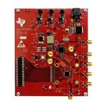
AFE707xEVM Evaluation Module
This is the user’s guide for the AFE707xEVM evaluation module (EVM). The AFE7070/71 is a dual 14-bit
65-MSPS digital-to-analog converter with an integrated quadrature modulator. The NCO and LVDS output
functions are not available with the AFE7071 but the AFE7070 has both functions. This is the sole
difference between the AFE7070 and the AFE7071. Hereafter, the AFE707x is referred to as AFE7070.
The EVM also includes the CDCM7005 clock synchronizer, which provides the necessary clocks for the
AFE and pattern generator. This EVM is ideally suited for mating with the TSW1400 pattern generation
card for evaluating WCDMA, LTE, or other high-performance modulation schemes.
1
2
3
Contents
Hardware Overview.......................................................................................................... 2
1.1
EVM Block Diagram ................................................................................................ 2
1.2
Parallel Input Data .................................................................................................. 2
1.3
Analog Inputs/Outputs.............................................................................................. 2
1.4
Clocking Options .................................................................................................... 3
1.5
Power Supply Options ............................................................................................. 4
Software Control ............................................................................................................. 5
2.1
Installation Instructions ............................................................................................. 5
2.2
Software Operation ................................................................................................. 5
Basic Test Procedure ....................................................................................................... 8
3.1
Test Block Diagram ................................................................................................. 8
3.2
Test Setup Connections ........................................................................................... 8
3.3
TSW1400 Quick-Start Operation ................................................................................. 9
3.4
AFE7070 Software Quick-Start Guide .......................................................................... 10
3.5
AFE7070 Performance Results ................................................................................. 11
List of Figures
1
EVM Block Diagram ......................................................................................................... 2
2
EVM Power Architecture .................................................................................................... 4
3
Screen Shot of AFE7070 Tab .............................................................................................. 5
4
Screen Shot of CDCM7005 Tab ........................................................................................... 7
5
Test Setup Block Diagram .................................................................................................. 8
6
TSW1400 Programming GUI ............................................................................................... 9
7
TSW1400 Multitone Pattern............................................................................................... 10
8
Two-Tone IMD Performance: LO = 2.1 GHz, DAC Rate = 65 MSPS, IF = 4.5 MHz and 5.5 MHz
SLOU337A – March 2012 – Revised July 2015
Submit Documentation Feedback
.............
AFE707xEVM Evaluation Module
Copyright © 2012–2015, Texas Instruments Incorporated
11
1
�Hardware Overview
1
www.ti.com
Hardware Overview
This section describes the EVM hardware and how it can be modified to evaluate the AFE7070 in various
configurations.
1.1
EVM Block Diagram
Figure 1 shows a simplified block diagram of the EVM in its default configuration.
VCXO
SMA
REF
10 MHz
Reference
3
USB
Port
Y4
SMA
CDCM7005
Clock Synchronizer +
Jitter Cleaner
SPI
3.3 V
Y1
Y3
USB-to-Parallel
FIFO
DC/DC Converter
Power
Jack
4
CLKIO
DACCLK
SPI
2-Row
Header
3.3 V
DC/DC Converter
14
1.8 V
D[13:0]
DC/DC Converter
AFE7070
DAC + Modulator
SMA
RF
SMA
LVDS
SMA
LO
Figure 1. EVM Block Diagram
1.2
Parallel Input Data
Parallel input data is supplied to the EVM by header J8. This header can be connected to the TSW1400
CMOS outputs by a parallel CMOS connector board.
1.3
1.3.1
Analog Inputs/Outputs
Local Oscillator
A local oscillator (LO) signal must be provided via the SMA connector J10. This signal’s amplitude must
be between –5 dBm and 5 dBm with a frequency between 100 MHz and 2.7 GHz. The signal at the SMA
connector is ac-coupled into the AFE7070’s LOP pin; LON is ac-terminated with 50 Ω.
1.3.2
External Clock Input
Provide an external clock signal by the SMA connector J4. By default, this signal is ac-coupled by a 0.01
µF capacitor and then rebiased to a common-mode dc voltage of 1.3 V at the CDCM7005’s VCXO_IN
input. The ac load impedance is 50 Ω. The input signal level can be between 1 V and 2.6 V peak-to-peak.
2
AFE707xEVM Evaluation Module
SLOU337A – March 2012 – Revised July 2015
Submit Documentation Feedback
Copyright © 2012–2015, Texas Instruments Incorporated
�Hardware Overview
www.ti.com
1.3.3
RF Out
The AFE7070’s RF output (pin RFOUT) is ac-coupled by a 100 pF capacitor to the SMA connector J3.
This output can be connected directly to a 50-Ω spectrum analyzer or other test equipment.
1.3.4
LVDS Output
In the EVM’s default configuration, the AFE7070’s LVDS_P and LVDS_N outputs are routed directly to
SMA connectors J1 and J2, respectively. If desired, onboard termination can be added by populating
resistor R53; otherwise, properly terminate the signal with 100-Ω differential impedance at its sink.
The complementary LVDS outputs also can be converted to a single-ended signal for ease of
measurement. To do this, remove resistors R17 and R50, and place 0-Ω resistors at R21 and R38. This
routes the LVDS outputs to transformer T6 (connected to SMA connector J14) and disconnects them from
connectors J1 and J2. Place a resistor at position R53 to make the differential impedance seen by the
LVDS outputs equal to 100 Ω. If the SMA connector J14 is connected to 50-Ω test equipment, the value of
R53 must be 200 Ω, because the 50-Ω impedance is transformed to 200 Ω on the primary side due to
transformer T6’s 4-to-1 impedance ratio.
The AFE7071 does not have this function.
1.4
Clocking Options
This EVM accommodates a wide range of clocking options. The AFE7070 has four clocking modes: Dual
Input Clock, Dual Output Clock, Single Differential DDR Clock, and Single Differential SDR Clock. See the
device data sheet for a detailed description of these four modes. The clock signals on the EVM can be
generated with the CDCM7005 or supplied externally. Similarly, the reference and VCXO inputs to the
CDCM7005 can come from onboard oscillators or other sources.
1.4.1
Default Configuration
By default, the CDCM7005 is configured to use an onboard 10-MHz reference and external VCXO input
signal to generate the AFE7070’s DACCLK and CLKIO signals. This is suitable for evaluating the
AFE7070’s Dual Input Clock, Single Differential DDR, and Single Differential SDR modes. A third
CDCM7005 output is routed to SMA connector J5. This signal can be sent to the TSW1400’s CMOS clock
input to align and synchronize the input data bus. Note that external equipment may be needed to add a
delay to this clock signal such that proper setup and hold times are maintained.
1.4.2
Dual Output Clock Mode
In Dual Output Clock mode, the AFE7070’s CLKIO pin becomes an output that can be used to drive a
digital source such as the TSW1400. To use this mode, the user must remove resistor R18 connecting
CLKIO to the CDCM7005’s output and instead populate resistor R25. This routes the CLKIO signal to
SMA connector J11. This output then can be connected to the TSW1400 CMOS clock input.
1.4.3
Onboard VCXO
If desired, a VCXO can be installed on the board at position VCXO1 to provide an input clock source to
the CDCM7005. In addition to populating the VCXO, remove resistor R13 and populate C29 with a 0-Ω
resistor. This allows for dc-coupling a differential LVPECL-output VCXO (such as the TCO-2111) to the
VCXO_IN and VCXO_INB inputs of the CDCM7005.
1.4.4
External Reference Clock
The CDCM7005’s reference clock can be supplied externally as well. Because the CDCM7005 has two
reference inputs (primary and secondary), it is possible to simply connect an external CMOS-level clock to
SMA connector J6. The applied signal is ac-coupled and rebiased to a dc common-mode voltage of 1.65
V (midsupply), then applied to the CDCM7005’s PRI_REF input. If required, add a termination resistor to
position R26. Depending on the software settings, the CDCM7005 may automatically switch to the
external clock signal (automatic mode), or require the use of jumper JP3 to select it (manual mode).
SLOU337A – March 2012 – Revised July 2015
Submit Documentation Feedback
AFE707xEVM Evaluation Module
Copyright © 2012–2015, Texas Instruments Incorporated
3
�Hardware Overview
1.4.5
www.ti.com
Bypass CDCM7005
Bypassing the CDCM7005 entirely and simply supplying external clocks to the AFE7070 is possible. You
can use the SMA connector J12 to supply the LVPECL-level DACCLK signal if you install capacitors C129
and C130 and remove C102 and C103. A termination resistor may be placed at position R54, although
resistor R55 provides 100-Ω differential termination at the AFE7070’s DACCLK P and N inputs. When
setting the external clock’s amplitude, keep in mind the 2-to-1 impedance ratio of the transformer used for
single-ended-to-differential conversion.
Note that depending on the AFE7070’s clock mode, you may need to be send separate clock signals to
CLKIO or to the digital source as well. The SMA connector J11 can supply CLKIO, providing that you
install resistor R25 and remove R18. Connecting the TSW1400 CMOS clock input to an external clock
source is possible as well. Ensure that these various clock signals are synchronized and do not drift with
respect to one another.
1.5
Power Supply Options
The EVM provides multiple options for powering the AFE7070 and CDCM7005 integrated circuits (IC). By
default, users can power the board with a 6-Vdc adapter. Switched-mode dc/dc (buck) converters step
down this voltage to the necessary 3.3-V and 1.8-V rail voltages. If desired, users can use LDOs or bench
supplies rather than switching power supplies. Figure 2 provides a simplified block diagram of the EVM’s
power architecture showing how jumper settings can be used to enable and disable various power supply
ICs. Also, disconnecting all jumpers and providing the necessary rail voltages directly to test points TP7,
TP6, and TP8 is possible.
6 V in
TPS2400
6V
Under/Overvoltage
Protection IC
TPS7A4501 5 V JP6
1.5-A Low Noise
Adjustable LDO
1
TPS62237
2
2-MHz, 500-mA
DC/DC Converter
JP7
1
2
3
4
TPS79533
500-mA Low Noise
Fixed Output LDO
TPS62237
2-MHz, 500-mA
DC/DC Converter
JP9
1
2
3
4
TPS79533
500-mA Low Noise
Fixed Output LDO
TPS62237
2-MHz, 500-mA
DC/DC Converter
JP12
1
2
3
4
TPS79518
500-mA Low Noise
Fixed Output LDO
3.3 V
JP8
1
2
3
3.3 V
CDC
3.3 V
3.3 V
1
2
3
JP10
3.3 V
AFE
3.3 V
1.8 V
1
2
3
JP11
1.8 V
AFE
1.8 V
Figure 2. EVM Power Architecture
For a detailed illustration of the EVM’s power supplies, see the circuit schematic included in the Design
Files on the AFE7070EVM and AFE7071EVM tool pages.
4
AFE707xEVM Evaluation Module
SLOU337A – March 2012 – Revised July 2015
Submit Documentation Feedback
Copyright © 2012–2015, Texas Instruments Incorporated
�Software Control
www.ti.com
2
Software Control
2.1
Installation Instructions
•
•
•
•
•
2.2
Open the folder named AFE7070_Installer_vxpx (xpx represents the latest version).
Run Setup.exe.
Follow the on-screen instructions.
Once installed, launch the software by clicking on the AFE7070_GUI_vxpx program in Start → Texas
Instruments DACs
When plugging in the USB cable for the first time, you are prompted to install the USB drivers.
– When a pop-up screen opens, select Continue Downloading.
– Follow the on-screen instructions to install the USB drivers
– If needed, you can access the drivers directly in the install directory
Software Operation
The user interface is divided into two tabs, one containing controls for the AFE7070 and the other
containing controls for the CDCM7005.
2.2.1
AFE7070 Controls
A screen shot of the AFE7070 tab is shown in Figure 3.
Figure 3. Screen Shot of AFE7070 Tab
The controls for the AFE7070 are divided into the following sections:
• Power. These controls consist of binary switches that toggle various power-down and sleep states.
• SYNC Settings. These settings control the device synchronization. The switch marked Synchronize
corresponds to the SYNC bit in the AFE7070 register map, and activating this switch writes a 1 to this
bit.
• FIFO Settings. This section is only active when the device is in Dual Input Clock mode. It controls the
SLOU337A – March 2012 – Revised July 2015
Submit Documentation Feedback
AFE707xEVM Evaluation Module
Copyright © 2012–2015, Texas Instruments Incorporated
5
�Software Control
•
•
•
•
•
•
•
•
2.2.2
www.ti.com
FIFO pointer offset and various FIFO alarms.
Clock Settings. This section allows the user to specify which clock mode is desired as well as trim the
clock RC filter. Ensuring that the other AFE7070 settings and CDCM7005 settings are consistent with
the choice of clock mode is important. For reference, the following is a summary of the relevant
settings for each mode:
– Dual Input Clock – Configure CLKIO on the CDCM7005 tab to be an active CMOS signal at either
1x or 2x the desired sampling rate. Set DACCLK to active, LVPECL levels, and 2x the desired
sampling rate. Set the data type in the AFE7070 tab’s Digital Input Settings section to either IQ or
Phase data. Configure the FIFO as desired. Connect the CDC OUT output via the SMA to the
TSW1400, and configure as an active CMOS output at the same frequency as DACCLK.
– Dual Output Clock – In this mode, CLKIO is an output and must not be connected to the
CDCM7005 (see Section 1.4.2 for the necessary hardware modifications). DACCLK must be an
active LVPECL clock at 2x the desired sampling rate. Set the data type in the AFE7070 tab’s Digital
Input Settings section to either IQ or Phase data. In this mode, the FIFO is disabled automatically.
– Single Differential DDR Clock – CLKIO is not used in this mode, so it can be disabled in the
CDCM7005 settings. An LVPECL-level DACCLK must be provided at 1x the desired sampling rate.
Either IQ or Phase data is allowed, and the FIFO is disabled automatically. Connect the CDC OUT
output to the TSW1400 by way of the SMA, and configure it as an active CMOS output at 2x the
DACCLK frequency.
– Single Differential SDR Clock – CLKIO is unused and can be disabled. Provide an LVPECL-level
DACCLK at 1x the desired sampling rate. Only use this mode for Phase data. Connect the CDC
OUT output to the TSW1400 by way of the SMA, and configure it as an active CMOS output at 1x
the DACCLK frequency.
Mixer/NCO Settings. Use these controls to enable or disable the AFE7070’s mixer stage as well as
adjust its frequency and initial phase. Note that the frequency values input must be the actual desired
NCO frequency in MHz, not the value to be stored in the frequency registers. The AFE7071 does not
have this function.
Digital Input Settings. These controls affect the way the AFE7070 interprets its input data.
Misc. Digital Signals. These controls affect the way the AFE7070 interprets other digital data. Note
that the GUI generates SPI commands based on a 3-wire serial interface (SIF).
QMC Settings. These controls allow the user to adjust QMC offset (to reduce carrier feedthrough) and
gain/phase (to improve sideband suppression).
LVDS Clock Divider. This section sets the divide ratio for the LVDS output. Note that this output’s
frequency can range from 100 MHz to 800 MHz.
Analog Output Settings. These controls affect the internal DAC outputs. The full-scale current setting
is 15. The Trim Analog Filters slider can adjust the corner frequency of the baseband low-pass filter.
The maximum filter corner is 10 MHz.
Atest. These controls activate various test modes and are not useful to most users.
CDCM7005 Controls
The CDCM7005 tab provides full programming control of the CDCM7005 device. Figure 4 displays a
screen shot of this tab. . Not all of the functions may be of interest in evaluating AFE7070 performance.
The tab is divided into three sections:
• Advanced Options. These settings provide advanced control of the CDCM7005 device. Their
functions are beyond the scope of this document. For a detailed description of these settings, consult
the CDCM7005 data sheet (SCAS793).
• Clock & PLL Options. This section is only enabled when the CDCM7005 is in PLL mode and allows
the user to specify (manually or automatically) the necessary M and N divider settings to produce a
desired VCXO frequency output.
• Output Options. These controls allow configuration for various CDCM7005 outputs. The only outputs
of interest are Y1 (the AFE7070’s CLK_IO), Y3 (the AFE7070’s DACCLK), and Y4 (CDC OUT, which
can be used to provide a clock to the TSW1400). The user can specify the output levels (LVPECL or
LVCMOS), a divide ratio, and whether or not each signal is active or high-impedance.
6
AFE707xEVM Evaluation Module
SLOU337A – March 2012 – Revised July 2015
Submit Documentation Feedback
Copyright © 2012–2015, Texas Instruments Incorporated
�Software Control
www.ti.com
Figure 4. Screen Shot of CDCM7005 Tab
2.2.3
General GUI Controls
The following is a summary of the various other GUI controls:
• Reset USB Port. This button assigns a new handle for the USB connection. Use it whenever a device
communication failure occurs.
• One Shot. This button can be enabled to run the program only once rather than as a loop.
• Exit. This buttons exits the GUI.
• Display Pane. This pane takes up most of the right side of the GUI and is used to display which
register settings are being written to or read from the AFE7070.
• Register Controls
– Send All. This command sends all the GUI settings to the AFE7070 and CDCM7005 registers.
– Read All. This command reads back the register values of the AFE7070 and display them in the
display pane.
– Load Regs. This command loads the contents of a text file into both the AFE7070 and CDCM7005
registers (as applicable).
– Save All Regs. This command saves the AFE7070 and CDCM7005 register settings to a text file.
– Save AFE Regs. This command saves the AFE7070 register settings to a text file.
– Save CDC Regs. This command saves the CDCM7005 register settings to a text file.
SLOU337A – March 2012 – Revised July 2015
Submit Documentation Feedback
AFE707xEVM Evaluation Module
Copyright © 2012–2015, Texas Instruments Incorporated
7
�Basic Test Procedure
3
www.ti.com
Basic Test Procedure
This section outlines the basic procedure for testing the EVM.
3.1
Test Block Diagram
Figure 5 displays the test setup for general testing of the AFE7070 with the TSW1400 pattern generation
card.
Clock
Generator
PC
USB
USB
J5
J7
TSW1400
J1
J5
CMOS
Connector
Board
AFE7070 EVM
Spectrum
Analyzer
J8
J12
5-V Adapter
J4
J3
J7
J9
J10
6-V Adapter
RF Signal
Generator
Figure 5. Test Setup Block Diagram
3.2
Test Setup Connections
•
•
•
Connect the AFE7071 EVM to the computer via USB cable.
Connect 6-V adapter to J9.
Launch the AFE7071EVM GUI and click Reset USB Port.
NOTE: Always connect the AFE7071 EVM and click Reset USB Port before connecting the
TSW1400, otherwise, you will not be able to connect with the AFE7071 EVM board.
•
•
•
•
•
•
•
•
8
Connect the signal generator to theJ4 connector (EXT VCXO) on the AFE7071 EVM. Set the
frequency of the signal generator to 130 MHz and amplitude to 0 dBm.
Connect LO signal from the second signal generator to the J10 connector (LO IN). Set the frequency of
the signal generator to 2.1 GHz and amplitude to 5 dBm.
Connect J3 (RFOUT) to the spectrum analyzer.
Connect the TSW1400 to the computer via USB cable.
Connect the J1 (CMOS_INTERFACE) connector on the TSW1400 to AFE7071 EVM’s J8 connector.
Make sure pin 1 of the J1 connector is aligned with pin 1 on the J8 connector before connecting.
Connect the J7 (CMOS_CLK) on TSW1400 to J5 (CDC OUT) connector on AFE7071 EVM.
Connect 5-V adapter to J12 on TSW1400.
Turn the switch (SW7) to the On position.
AFE707xEVM Evaluation Module
SLOU337A – March 2012 – Revised July 2015
Submit Documentation Feedback
Copyright © 2012–2015, Texas Instruments Incorporated
�Basic Test Procedure
www.ti.com
3.3
TSW1400 Quick-Start Operation
The TSW1400 is a high speed data capture and pattern generator board used to evaluate performances
of a wide range of TI high-speed analog-to-digital converters (ADC) and digital-to-analog converters
(DAC).
See the TSW1400 user’s guide (SLWU079) for a more detailed explanation of the TSW1400 setup and
operation. This document assumes that High Speed Data Pro software is installed and functioning
properly. The front panel of TSW1400 is shown in Figure 6 and Figure 7. Change the following parameters
from the default settings.
Multitone Setup from Default Configuration
• Launch the High Speed Data Convertor Pro software. Click OK on the Select Board pop up message.
• Select the DAC tab.
• Select CMOS_AFE7070 from the top left drop-down menu.
• Set the Data rate to "65" MHz and DAC Option to Offset Bin.
• Set I/Q Multitone Generator → Tone BW to "1M", set # (of tones) to "2", and Tone Center to "5M".
• Under Tone selection, select Complex.
• Click the Create Tones button.
• Click Send.
Figure 6. TSW1400 Programming GUI
SLOU337A – March 2012 – Revised July 2015
Submit Documentation Feedback
AFE707xEVM Evaluation Module
Copyright © 2012–2015, Texas Instruments Incorporated
9
�Basic Test Procedure
www.ti.com
Figure 7. TSW1400 Multitone Pattern
3.4
AFE7070 Software Quick-Start Guide
•
•
•
•
•
•
In the Clock Settings section, set the clock mode to Dual Input Clock.
If the LVDS output is not connected to anything, disable it using the LVDS Power Down switch under
the Power heading.
Select the CDCM7005 tab to adjust the output clock signals:
– Y1 (AFE7070’s CLK_IO) must be LVCMOS, with Y1A set to active rather than 3-state.
– Y3 (AFE7070’s DACCLK) must be LVPECL, with both Y3A and Y3B set to active.
– Y4 (CDC Out) must be LVCMOS, with Y4A set to active.
Press the Send All button in the Register Controls section.
Monitor the RF output signal on a spectrum analyzer.
Monitor the output signal at the RF output connector. If the LO input frequency is set to 2.1 GHz and
the digital inputs are configured to be tones at 4.5 MHz and 5.5 MHz, the RF output looks like two
tones placed at 2004.5 MHz and 2005.5 MHz as seen in Figure 8.
If no output is observed on the spectrum analyzer, reset the AFE7071 by pressing the SW1 switch on the
AFE7071 EVM.
10
AFE707xEVM Evaluation Module
SLOU337A – March 2012 – Revised July 2015
Submit Documentation Feedback
Copyright © 2012–2015, Texas Instruments Incorporated
�Basic Test Procedure
www.ti.com
3.5
AFE7070 Performance Results
Figure 8 shows the typical two-tone performance of the AFE7070 EVM from the preceding setup.
Figure 8. Two-Tone IMD Performance: LO = 2.1 GHz, DAC Rate = 65 MSPS, IF = 4.5 MHz and 5.5 MHz
Note that some part-to-part variations can yield significantly improved two-tone IP3 performance. The
performance plots in this document show typical responses.
Revision History
Changes from Original (March 2012) to A Revision ....................................................................................................... Page
•
•
•
•
•
•
•
•
•
•
•
Changed TSW3100 to TSW1400 in text and images throughout the entire document. ......................................... 1
Changed Test Setup Block Diagram image, replaced Ethernet with USB and changed the TSW3100 block to
TSW1400. .................................................................................................................................. 8
Changed entire Test Setup Connections section. .................................................................................... 8
Changed entire TSW1400 Quick-Start Operation section. .......................................................................... 9
Changed TSW1400 Programming GUI image. ....................................................................................... 9
Changed TSW1400 Multitone Pattern image. ....................................................................................... 10
Deleted first bullet in AFE7070 Software Quick-Start Guide section. ............................................................. 10
Changed all the values in the last bullet of the AFE7070 Software Quick-Start Guide section. .............................. 10
Added paragraph to the end of the AFE7070 Software Quick-Start Guide section. ............................................ 10
Changed Two-Tone IMD Performance: image. Also changed IF values to 4.5 MHz and 5.5 MHz. ......................... 11
Deleted WCDMA ACPR: LO = 2 GHz, DAC Rate = 57.6 MHz, 0-MHz Offset image. ......................................... 11
NOTE: Page numbers for previous revisions may differ from page numbers in the current version.
SLOU337A – March 2012 – Revised July 2015
Submit Documentation Feedback
Revision History
Copyright © 2012–2015, Texas Instruments Incorporated
11
�STANDARD TERMS AND CONDITIONS FOR EVALUATION MODULES
1.
Delivery: TI delivers TI evaluation boards, kits, or modules, including any accompanying demonstration software, components, or
documentation (collectively, an “EVM” or “EVMs”) to the User (“User”) in accordance with the terms and conditions set forth herein.
Acceptance of the EVM is expressly subject to the following terms and conditions.
1.1 EVMs are intended solely for product or software developers for use in a research and development setting to facilitate feasibility
evaluation, experimentation, or scientific analysis of TI semiconductors products. EVMs have no direct function and are not
finished products. EVMs shall not be directly or indirectly assembled as a part or subassembly in any finished product. For
clarification, any software or software tools provided with the EVM (“Software”) shall not be subject to the terms and conditions
set forth herein but rather shall be subject to the applicable terms and conditions that accompany such Software
1.2 EVMs are not intended for consumer or household use. EVMs may not be sold, sublicensed, leased, rented, loaned, assigned,
or otherwise distributed for commercial purposes by Users, in whole or in part, or used in any finished product or production
system.
2
Limited Warranty and Related Remedies/Disclaimers:
2.1 These terms and conditions do not apply to Software. The warranty, if any, for Software is covered in the applicable Software
License Agreement.
2.2 TI warrants that the TI EVM will conform to TI's published specifications for ninety (90) days after the date TI delivers such EVM
to User. Notwithstanding the foregoing, TI shall not be liable for any defects that are caused by neglect, misuse or mistreatment
by an entity other than TI, including improper installation or testing, or for any EVMs that have been altered or modified in any
way by an entity other than TI. Moreover, TI shall not be liable for any defects that result from User's design, specifications or
instructions for such EVMs. Testing and other quality control techniques are used to the extent TI deems necessary or as
mandated by government requirements. TI does not test all parameters of each EVM.
2.3 If any EVM fails to conform to the warranty set forth above, TI's sole liability shall be at its option to repair or replace such EVM,
or credit User's account for such EVM. TI's liability under this warranty shall be limited to EVMs that are returned during the
warranty period to the address designated by TI and that are determined by TI not to conform to such warranty. If TI elects to
repair or replace such EVM, TI shall have a reasonable time to repair such EVM or provide replacements. Repaired EVMs shall
be warranted for the remainder of the original warranty period. Replaced EVMs shall be warranted for a new full ninety (90) day
warranty period.
3
Regulatory Notices:
3.1 United States
3.1.1
Notice applicable to EVMs not FCC-Approved:
This kit is designed to allow product developers to evaluate electronic components, circuitry, or software associated with the kit
to determine whether to incorporate such items in a finished product and software developers to write software applications for
use with the end product. This kit is not a finished product and when assembled may not be resold or otherwise marketed unless
all required FCC equipment authorizations are first obtained. Operation is subject to the condition that this product not cause
harmful interference to licensed radio stations and that this product accept harmful interference. Unless the assembled kit is
designed to operate under part 15, part 18 or part 95 of this chapter, the operator of the kit must operate under the authority of
an FCC license holder or must secure an experimental authorization under part 5 of this chapter.
3.1.2
For EVMs annotated as FCC – FEDERAL COMMUNICATIONS COMMISSION Part 15 Compliant:
CAUTION
This device complies with part 15 of the FCC Rules. Operation is subject to the following two conditions: (1) This device may not
cause harmful interference, and (2) this device must accept any interference received, including interference that may cause
undesired operation.
Changes or modifications not expressly approved by the party responsible for compliance could void the user's authority to
operate the equipment.
FCC Interference Statement for Class A EVM devices
NOTE: This equipment has been tested and found to comply with the limits for a Class A digital device, pursuant to part 15 of
the FCC Rules. These limits are designed to provide reasonable protection against harmful interference when the equipment is
operated in a commercial environment. This equipment generates, uses, and can radiate radio frequency energy and, if not
installed and used in accordance with the instruction manual, may cause harmful interference to radio communications.
Operation of this equipment in a residential area is likely to cause harmful interference in which case the user will be required to
correct the interference at his own expense.
SPACER
SPACER
SPACER
SPACER
SPACER
SPACER
SPACER
SPACER
�FCC Interference Statement for Class B EVM devices
NOTE: This equipment has been tested and found to comply with the limits for a Class B digital device, pursuant to part 15 of
the FCC Rules. These limits are designed to provide reasonable protection against harmful interference in a residential
installation. This equipment generates, uses and can radiate radio frequency energy and, if not installed and used in accordance
with the instructions, may cause harmful interference to radio communications. However, there is no guarantee that interference
will not occur in a particular installation. If this equipment does cause harmful interference to radio or television reception, which
can be determined by turning the equipment off and on, the user is encouraged to try to correct the interference by one or more
of the following measures:
•
•
•
•
Reorient or relocate the receiving antenna.
Increase the separation between the equipment and receiver.
Connect the equipment into an outlet on a circuit different from that to which the receiver is connected.
Consult the dealer or an experienced radio/TV technician for help.
3.2 Canada
3.2.1
For EVMs issued with an Industry Canada Certificate of Conformance to RSS-210
Concerning EVMs Including Radio Transmitters:
This device complies with Industry Canada license-exempt RSS standard(s). Operation is subject to the following two conditions:
(1) this device may not cause interference, and (2) this device must accept any interference, including interference that may
cause undesired operation of the device.
Concernant les EVMs avec appareils radio:
Le présent appareil est conforme aux CNR d'Industrie Canada applicables aux appareils radio exempts de licence. L'exploitation
est autorisée aux deux conditions suivantes: (1) l'appareil ne doit pas produire de brouillage, et (2) l'utilisateur de l'appareil doit
accepter tout brouillage radioélectrique subi, même si le brouillage est susceptible d'en compromettre le fonctionnement.
Concerning EVMs Including Detachable Antennas:
Under Industry Canada regulations, this radio transmitter may only operate using an antenna of a type and maximum (or lesser)
gain approved for the transmitter by Industry Canada. To reduce potential radio interference to other users, the antenna type
and its gain should be so chosen that the equivalent isotropically radiated power (e.i.r.p.) is not more than that necessary for
successful communication. This radio transmitter has been approved by Industry Canada to operate with the antenna types
listed in the user guide with the maximum permissible gain and required antenna impedance for each antenna type indicated.
Antenna types not included in this list, having a gain greater than the maximum gain indicated for that type, are strictly prohibited
for use with this device.
Concernant les EVMs avec antennes détachables
Conformément à la réglementation d'Industrie Canada, le présent émetteur radio peut fonctionner avec une antenne d'un type et
d'un gain maximal (ou inférieur) approuvé pour l'émetteur par Industrie Canada. Dans le but de réduire les risques de brouillage
radioélectrique à l'intention des autres utilisateurs, il faut choisir le type d'antenne et son gain de sorte que la puissance isotrope
rayonnée équivalente (p.i.r.e.) ne dépasse pas l'intensité nécessaire à l'établissement d'une communication satisfaisante. Le
présent émetteur radio a été approuvé par Industrie Canada pour fonctionner avec les types d'antenne énumérés dans le
manuel d’usage et ayant un gain admissible maximal et l'impédance requise pour chaque type d'antenne. Les types d'antenne
non inclus dans cette liste, ou dont le gain est supérieur au gain maximal indiqué, sont strictement interdits pour l'exploitation de
l'émetteur
3.3 Japan
3.3.1
Notice for EVMs delivered in Japan: Please see http://www.tij.co.jp/lsds/ti_ja/general/eStore/notice_01.page 日本国内に
輸入される評価用キット、ボードについては、次のところをご覧ください。
http://www.tij.co.jp/lsds/ti_ja/general/eStore/notice_01.page
3.3.2
Notice for Users of EVMs Considered “Radio Frequency Products” in Japan: EVMs entering Japan may not be certified
by TI as conforming to Technical Regulations of Radio Law of Japan.
If User uses EVMs in Japan, not certified to Technical Regulations of Radio Law of Japan, User is required by Radio Law of
Japan to follow the instructions below with respect to EVMs:
1.
2.
3.
Use EVMs in a shielded room or any other test facility as defined in the notification #173 issued by Ministry of Internal
Affairs and Communications on March 28, 2006, based on Sub-section 1.1 of Article 6 of the Ministry’s Rule for
Enforcement of Radio Law of Japan,
Use EVMs only after User obtains the license of Test Radio Station as provided in Radio Law of Japan with respect to
EVMs, or
Use of EVMs only after User obtains the Technical Regulations Conformity Certification as provided in Radio Law of Japan
with respect to EVMs. Also, do not transfer EVMs, unless User gives the same notice above to the transferee. Please note
that if User does not follow the instructions above, User will be subject to penalties of Radio Law of Japan.
SPACER
SPACER
SPACER
SPACER
SPACER
�【無線電波を送信する製品の開発キットをお使いになる際の注意事項】 開発キットの中には技術基準適合証明を受けて
いないものがあります。 技術適合証明を受けていないもののご使用に際しては、電波法遵守のため、以下のいずれかの
措置を取っていただく必要がありますのでご注意ください。
1.
2.
3.
電波法施行規則第6条第1項第1号に基づく平成18年3月28日総務省告示第173号で定められた電波暗室等の試験設備でご使用
いただく。
実験局の免許を取得後ご使用いただく。
技術基準適合証明を取得後ご使用いただく。
なお、本製品は、上記の「ご使用にあたっての注意」を譲渡先、移転先に通知しない限り、譲渡、移転できないものとします。
上記を遵守頂けない場合は、電波法の罰則が適用される可能性があることをご留意ください。 日本テキサス・イ
ンスツルメンツ株式会社
東京都新宿区西新宿6丁目24番1号
西新宿三井ビル
3.3.3
Notice for EVMs for Power Line Communication: Please see http://www.tij.co.jp/lsds/ti_ja/general/eStore/notice_02.page
電力線搬送波通信についての開発キットをお使いになる際の注意事項については、次のところをご覧くださ
い。http://www.tij.co.jp/lsds/ti_ja/general/eStore/notice_02.page
SPACER
4
EVM Use Restrictions and Warnings:
4.1 EVMS ARE NOT FOR USE IN FUNCTIONAL SAFETY AND/OR SAFETY CRITICAL EVALUATIONS, INCLUDING BUT NOT
LIMITED TO EVALUATIONS OF LIFE SUPPORT APPLICATIONS.
4.2 User must read and apply the user guide and other available documentation provided by TI regarding the EVM prior to handling
or using the EVM, including without limitation any warning or restriction notices. The notices contain important safety information
related to, for example, temperatures and voltages.
4.3 Safety-Related Warnings and Restrictions:
4.3.1
User shall operate the EVM within TI’s recommended specifications and environmental considerations stated in the user
guide, other available documentation provided by TI, and any other applicable requirements and employ reasonable and
customary safeguards. Exceeding the specified performance ratings and specifications (including but not limited to input
and output voltage, current, power, and environmental ranges) for the EVM may cause personal injury or death, or
property damage. If there are questions concerning performance ratings and specifications, User should contact a TI
field representative prior to connecting interface electronics including input power and intended loads. Any loads applied
outside of the specified output range may also result in unintended and/or inaccurate operation and/or possible
permanent damage to the EVM and/or interface electronics. Please consult the EVM user guide prior to connecting any
load to the EVM output. If there is uncertainty as to the load specification, please contact a TI field representative.
During normal operation, even with the inputs and outputs kept within the specified allowable ranges, some circuit
components may have elevated case temperatures. These components include but are not limited to linear regulators,
switching transistors, pass transistors, current sense resistors, and heat sinks, which can be identified using the
information in the associated documentation. When working with the EVM, please be aware that the EVM may become
very warm.
4.3.2
EVMs are intended solely for use by technically qualified, professional electronics experts who are familiar with the
dangers and application risks associated with handling electrical mechanical components, systems, and subsystems.
User assumes all responsibility and liability for proper and safe handling and use of the EVM by User or its employees,
affiliates, contractors or designees. User assumes all responsibility and liability to ensure that any interfaces (electronic
and/or mechanical) between the EVM and any human body are designed with suitable isolation and means to safely
limit accessible leakage currents to minimize the risk of electrical shock hazard. User assumes all responsibility and
liability for any improper or unsafe handling or use of the EVM by User or its employees, affiliates, contractors or
designees.
4.4 User assumes all responsibility and liability to determine whether the EVM is subject to any applicable international, federal,
state, or local laws and regulations related to User’s handling and use of the EVM and, if applicable, User assumes all
responsibility and liability for compliance in all respects with such laws and regulations. User assumes all responsibility and
liability for proper disposal and recycling of the EVM consistent with all applicable international, federal, state, and local
requirements.
5.
Accuracy of Information: To the extent TI provides information on the availability and function of EVMs, TI attempts to be as accurate
as possible. However, TI does not warrant the accuracy of EVM descriptions, EVM availability or other information on its websites as
accurate, complete, reliable, current, or error-free.
SPACER
SPACER
SPACER
SPACER
SPACER
SPACER
�SPACER
6.
Disclaimers:
6.1 EXCEPT AS SET FORTH ABOVE, EVMS AND ANY WRITTEN DESIGN MATERIALS PROVIDED WITH THE EVM (AND THE
DESIGN OF THE EVM ITSELF) ARE PROVIDED "AS IS" AND "WITH ALL FAULTS." TI DISCLAIMS ALL OTHER
WARRANTIES, EXPRESS OR IMPLIED, REGARDING SUCH ITEMS, INCLUDING BUT NOT LIMITED TO ANY IMPLIED
WARRANTIES OF MERCHANTABILITY OR FITNESS FOR A PARTICULAR PURPOSE OR NON-INFRINGEMENT OF ANY
THIRD PARTY PATENTS, COPYRIGHTS, TRADE SECRETS OR OTHER INTELLECTUAL PROPERTY RIGHTS.
6.2 EXCEPT FOR THE LIMITED RIGHT TO USE THE EVM SET FORTH HEREIN, NOTHING IN THESE TERMS AND
CONDITIONS SHALL BE CONSTRUED AS GRANTING OR CONFERRING ANY RIGHTS BY LICENSE, PATENT, OR ANY
OTHER INDUSTRIAL OR INTELLECTUAL PROPERTY RIGHT OF TI, ITS SUPPLIERS/LICENSORS OR ANY OTHER THIRD
PARTY, TO USE THE EVM IN ANY FINISHED END-USER OR READY-TO-USE FINAL PRODUCT, OR FOR ANY
INVENTION, DISCOVERY OR IMPROVEMENT MADE, CONCEIVED OR ACQUIRED PRIOR TO OR AFTER DELIVERY OF
THE EVM.
7.
USER'S INDEMNITY OBLIGATIONS AND REPRESENTATIONS. USER WILL DEFEND, INDEMNIFY AND HOLD TI, ITS
LICENSORS AND THEIR REPRESENTATIVES HARMLESS FROM AND AGAINST ANY AND ALL CLAIMS, DAMAGES, LOSSES,
EXPENSES, COSTS AND LIABILITIES (COLLECTIVELY, "CLAIMS") ARISING OUT OF OR IN CONNECTION WITH ANY
HANDLING OR USE OF THE EVM THAT IS NOT IN ACCORDANCE WITH THESE TERMS AND CONDITIONS. THIS OBLIGATION
SHALL APPLY WHETHER CLAIMS ARISE UNDER STATUTE, REGULATION, OR THE LAW OF TORT, CONTRACT OR ANY
OTHER LEGAL THEORY, AND EVEN IF THE EVM FAILS TO PERFORM AS DESCRIBED OR EXPECTED.
8.
Limitations on Damages and Liability:
8.1 General Limitations. IN NO EVENT SHALL TI BE LIABLE FOR ANY SPECIAL, COLLATERAL, INDIRECT, PUNITIVE,
INCIDENTAL, CONSEQUENTIAL, OR EXEMPLARY DAMAGES IN CONNECTION WITH OR ARISING OUT OF THESE
TERMS ANDCONDITIONS OR THE USE OF THE EVMS PROVIDED HEREUNDER, REGARDLESS OF WHETHER TI HAS
BEEN ADVISED OF THE POSSIBILITY OF SUCH DAMAGES. EXCLUDED DAMAGES INCLUDE, BUT ARE NOT LIMITED
TO, COST OF REMOVAL OR REINSTALLATION, ANCILLARY COSTS TO THE PROCUREMENT OF SUBSTITUTE GOODS
OR SERVICES, RETESTING, OUTSIDE COMPUTER TIME, LABOR COSTS, LOSS OF GOODWILL, LOSS OF PROFITS,
LOSS OF SAVINGS, LOSS OF USE, LOSS OF DATA, OR BUSINESS INTERRUPTION. NO CLAIM, SUIT OR ACTION SHALL
BE BROUGHT AGAINST TI MORE THAN ONE YEAR AFTER THE RELATED CAUSE OF ACTION HAS OCCURRED.
8.2 Specific Limitations. IN NO EVENT SHALL TI'S AGGREGATE LIABILITY FROM ANY WARRANTY OR OTHER OBLIGATION
ARISING OUT OF OR IN CONNECTION WITH THESE TERMS AND CONDITIONS, OR ANY USE OF ANY TI EVM
PROVIDED HEREUNDER, EXCEED THE TOTAL AMOUNT PAID TO TI FOR THE PARTICULAR UNITS SOLD UNDER
THESE TERMS AND CONDITIONS WITH RESPECT TO WHICH LOSSES OR DAMAGES ARE CLAIMED. THE EXISTENCE
OF MORE THAN ONE CLAIM AGAINST THE PARTICULAR UNITS SOLD TO USER UNDER THESE TERMS AND
CONDITIONS SHALL NOT ENLARGE OR EXTEND THIS LIMIT.
9.
Return Policy. Except as otherwise provided, TI does not offer any refunds, returns, or exchanges. Furthermore, no return of EVM(s)
will be accepted if the package has been opened and no return of the EVM(s) will be accepted if they are damaged or otherwise not in
a resalable condition. If User feels it has been incorrectly charged for the EVM(s) it ordered or that delivery violates the applicable
order, User should contact TI. All refunds will be made in full within thirty (30) working days from the return of the components(s),
excluding any postage or packaging costs.
10. Governing Law: These terms and conditions shall be governed by and interpreted in accordance with the laws of the State of Texas,
without reference to conflict-of-laws principles. User agrees that non-exclusive jurisdiction for any dispute arising out of or relating to
these terms and conditions lies within courts located in the State of Texas and consents to venue in Dallas County, Texas.
Notwithstanding the foregoing, any judgment may be enforced in any United States or foreign court, and TI may seek injunctive relief
in any United States or foreign court.
Mailing Address: Texas Instruments, Post Office Box 655303, Dallas, Texas 75265
Copyright © 2015, Texas Instruments Incorporated
spacer
�IMPORTANT NOTICE
Texas Instruments Incorporated and its subsidiaries (TI) reserve the right to make corrections, enhancements, improvements and other
changes to its semiconductor products and services per JESD46, latest issue, and to discontinue any product or service per JESD48, latest
issue. Buyers should obtain the latest relevant information before placing orders and should verify that such information is current and
complete. All semiconductor products (also referred to herein as “components”) are sold subject to TI’s terms and conditions of sale
supplied at the time of order acknowledgment.
TI warrants performance of its components to the specifications applicable at the time of sale, in accordance with the warranty in TI’s terms
and conditions of sale of semiconductor products. Testing and other quality control techniques are used to the extent TI deems necessary
to support this warranty. Except where mandated by applicable law, testing of all parameters of each component is not necessarily
performed.
TI assumes no liability for applications assistance or the design of Buyers’ products. Buyers are responsible for their products and
applications using TI components. To minimize the risks associated with Buyers’ products and applications, Buyers should provide
adequate design and operating safeguards.
TI does not warrant or represent that any license, either express or implied, is granted under any patent right, copyright, mask work right, or
other intellectual property right relating to any combination, machine, or process in which TI components or services are used. Information
published by TI regarding third-party products or services does not constitute a license to use such products or services or a warranty or
endorsement thereof. Use of such information may require a license from a third party under the patents or other intellectual property of the
third party, or a license from TI under the patents or other intellectual property of TI.
Reproduction of significant portions of TI information in TI data books or data sheets is permissible only if reproduction is without alteration
and is accompanied by all associated warranties, conditions, limitations, and notices. TI is not responsible or liable for such altered
documentation. Information of third parties may be subject to additional restrictions.
Resale of TI components or services with statements different from or beyond the parameters stated by TI for that component or service
voids all express and any implied warranties for the associated TI component or service and is an unfair and deceptive business practice.
TI is not responsible or liable for any such statements.
Buyer acknowledges and agrees that it is solely responsible for compliance with all legal, regulatory and safety-related requirements
concerning its products, and any use of TI components in its applications, notwithstanding any applications-related information or support
that may be provided by TI. Buyer represents and agrees that it has all the necessary expertise to create and implement safeguards which
anticipate dangerous consequences of failures, monitor failures and their consequences, lessen the likelihood of failures that might cause
harm and take appropriate remedial actions. Buyer will fully indemnify TI and its representatives against any damages arising out of the use
of any TI components in safety-critical applications.
In some cases, TI components may be promoted specifically to facilitate safety-related applications. With such components, TI’s goal is to
help enable customers to design and create their own end-product solutions that meet applicable functional safety standards and
requirements. Nonetheless, such components are subject to these terms.
No TI components are authorized for use in FDA Class III (or similar life-critical medical equipment) unless authorized officers of the parties
have executed a special agreement specifically governing such use.
Only those TI components which TI has specifically designated as military grade or “enhanced plastic” are designed and intended for use in
military/aerospace applications or environments. Buyer acknowledges and agrees that any military or aerospace use of TI components
which have not been so designated is solely at the Buyer's risk, and that Buyer is solely responsible for compliance with all legal and
regulatory requirements in connection with such use.
TI has specifically designated certain components as meeting ISO/TS16949 requirements, mainly for automotive use. In any case of use of
non-designated products, TI will not be responsible for any failure to meet ISO/TS16949.
Products
Applications
Audio
www.ti.com/audio
Automotive and Transportation
www.ti.com/automotive
Amplifiers
amplifier.ti.com
Communications and Telecom
www.ti.com/communications
Data Converters
dataconverter.ti.com
Computers and Peripherals
www.ti.com/computers
DLP® Products
www.dlp.com
Consumer Electronics
www.ti.com/consumer-apps
DSP
dsp.ti.com
Energy and Lighting
www.ti.com/energy
Clocks and Timers
www.ti.com/clocks
Industrial
www.ti.com/industrial
Interface
interface.ti.com
Medical
www.ti.com/medical
Logic
logic.ti.com
Security
www.ti.com/security
Power Mgmt
power.ti.com
Space, Avionics and Defense
www.ti.com/space-avionics-defense
Microcontrollers
microcontroller.ti.com
Video and Imaging
www.ti.com/video
RFID
www.ti-rfid.com
OMAP Applications Processors
www.ti.com/omap
TI E2E Community
e2e.ti.com
Wireless Connectivity
www.ti.com/wirelessconnectivity
Mailing Address: Texas Instruments, Post Office Box 655303, Dallas, Texas 75265
Copyright © 2015, Texas Instruments Incorporated
�