AFE7071
www.ti.com
SLOS789C – MAY 2012 – REVISED JANUARY 2012
Dual 14-Bit 65-MSPS Digital-to-Analog Converter With Integrated Analog Quadrature
Modulator
Check for Samples: AFE7071
FEATURES
APPLICATIONS
•
•
•
•
•
•
1
•
•
•
•
•
Maximum Sample Rate: 65 MSPS
Low Power: 334 mW
Interleaved CMOS Input, 1.8–3.3 V IOVDD
Input FIFO for Independent Data and DAC
Clocks
3- or 4-pin SPI Interface for Register
Programming
Quadrature Modulator Correction: Gain,
Phase, Offset for Sideband and LO
Suppression
Analog Baseband Filter With Programmable
Bandwidth: 20-MHz Maximum RF Bandwidth
RF Frequency Range: 100 MHz to 2.7 GHz
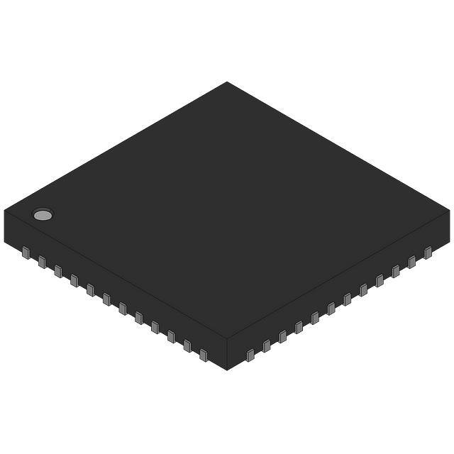
Package: 48-Pin QFN (7-mm × 7-mm)
Low-Power, Compact Software-Defined Radios
Femto- and Pico-Cell BTS
DESCRIPTION
The AFE7071 is a dual 14-bit 65-MSPS digital-toanalog
converter
(DAC)
with
integrated,
programmable fourth-order baseband filter and
analog quadrature modulator. The AFE7071 includes
additional digital signal-processing features such as a
quadrature modulator correction circuit, providing LO
and sideband suppression capability. The AFE7071
has an interleaved 14-bit 1.8-V to 3.3-V CMOS input.
The AFE7071 provides 20 MHz of RF signal
bandwidth with an RF output frequency range of 100
MHz to 2.7 GHz.
The AFE7071 package is a 7-mm × 7mm 48-pin QFN
package. The AFE7071 is specified over the full
industrial temperature range (–40°C to 85°C).
AVAILABLE OPTIONS
TA
–40°C to 85°C
ORDER CODE
AFE7071IRGZT
AFE7071IRGZR
PACKAGE DRAWING/TYPE
TRANSPORT MEDIA
RGZ / 48QFN quad flatpack no-lead
Tape and reel
QUANTITY
250
2500
1
Please be aware that an important notice concerning availability, standard warranty, and use in critical applications of
Texas Instruments semiconductor products and disclaimers thereto appears at the end of this data sheet.
PRODUCTION DATA information is current as of publication date.
Products conform to specifications per the terms of the Texas
Instruments standard warranty. Production processing does not
necessarily include testing of all parameters.
Copyright © 2012, Texas Instruments Incorporated
�AFE7071
SLOS789C – MAY 2012 – REVISED JANUARY 2012
www.ti.com
These devices have limited built-in ESD protection. The leads should be shorted together or the device placed in conductive foam
during storage or handling to prevent electrostatic damage to the MOS gates.
BLOCK DIAGRAM
SCLK
SDENB
SDIO
ALARM_SDO
RESETB
BG_BYP
SPI/
Registers
1.2-V
REF
Dual
DAC
Quadrature
Modulator
D[13:0]
RF_OUT
QMC
Demux
IQ_FLAG
SYNC_SLEEP
Baseband
Filter
CLK_IO
Clock
DACCLKP/N
¸2
LO_P/N
PIN CONFIGURATION
DACVDD18
MODVDD33
MODVDD33
FUSEVDD18
GND
RF_OUT
NC
GND
NC
MODVDD18
BG_BYP
DACVDD18
RGZ Package
(Top View)
DACCLKP
1
48 47 46 45 44 43 42 41 40 39 38 37
36
DACCLKN
2
35
TESTMODE
ATEST
CLKVDD18
3
34
ALARM_SDO
DACVDD33
4
33
LO_N
CLK_IO
5
32
LO_P
IQ_FLAG
6
31
SDENB
AFE7071
SYNC_SLEEP
7
30
SCLK
RESETB
8
29
SDIO
D13 (MSB)
9
28
D0 (LSB)
D12
10
27
D1
GND
11
26
GND
DVDD18
IOVDD
D2
D3
D4
D5
D6
D8
D7
D9
D10
D11
25
12
13 14 15 16 17 18 19 20 21 22 23 24
IOVDD
DVDD18
P0023-27
2
Submit Documentation Feedback
Copyright © 2012, Texas Instruments Incorporated
Product Folder Links: AFE7071
�AFE7071
www.ti.com
SLOS789C – MAY 2012 – REVISED JANUARY 2012
PIN FUNCTIONS
PIN
NAME
NO.
I/O
DESCRIPTION
MISC/SERIAL
CMOS output for ALARM condition, active-low. The ALARM output functionality is defined through the
CONFIG7 registers.
ALARM_SDO
34
O
RESETB
8
I
Resets the chip when low. 1.8-V to 3.3-V CMOS, set by IOVDD. Internal pullup
SCLK
30
I
Serial interface clock. 1.8-V to 3.3-V CMOS, set by IOVDD. Internal pulldown
SDENB
31
I
Active-low serial data enable, always an input. 1.8-V to 3.3-V CMOS, set by IOVDD. Internal pullup
SDIO
29
I/O
Bidirectional serial data in 3-pin mode (default). In 4-pin interface mode (CONFIG3 sif_4pin), the SDIO
pin is an input only. 1.8-V to 3.3-V CMOS, set by IOVDD. Internal pulldown
Single-ended input or output CMOS level clock for latching input data. 1.8-V to 3.3-V CMOS, set by
IOVDD.
Optionally, it can be used as the unidirectional data output in 4-pin serial interface mode (CONFIG3
sif_4pin = 1). 1.8-V to 3.3-V CMOS, set by IOVDD.
DATA/CLOCK INTERFACE
CLK_IO
5
I/O
D[13:0]
9, 10,
14–23,
27, 28
I
Data bits 0 through 13. D13 is the MSB, D0 is the LSB. For complex data, channel I and channel Q are
multiplexed. For NCO phase data, either 14 bits are transferred at the internal sample clock rate, or 8
MSBs and 8 LSBs are interleaved on D[13:6]. 1.8-V to 3.3-V CMOS, set by IOVDD. Internal pulldown
1, 2
I
Differential input clock for DACs.
IQ_FLAG
6
I
When register CONFIG1 iqswap is 0, IQ-FLAG high identifies the DACA sample in dual-input or dualoutput clock modes. 1.8-V or 3.3-V CMOS, set by IOVDD. Internal pulldown
SYNC_SLEEP
7
I
Multi-function. Sync signal for signal processing blocks, TX ENABLE or SLEEP function. Selectable via
SPI. 1.8-V to 3.3-V CMOS, set by IOVDD.
LO_P, LO_N
32, 33
I
Local oscillator input. Can be used differentially or single-ended by terminating the unused input
through a capacitor and 50-Ω resistor to GND.
NC
44, 45
–
No internal connection
42
O
Analog RF output
ATEST
36
O
Factory use only. Do not connect.
BG_BYP
47
I
Reference voltage decoupling – connect 0.1 µF to GND.
TESTMODE
35
I
Factory use only. Connect to GND.
13, 24
I
1.8-V to 3.3-V supply for CMOS I/Os
3
I
1.8 V
DVDD18
12, 25
I
1.8 V
DACVDD18
37, 48
I
1.8 V
MODVDD18
46
I
1.8 V
DACVDD33
4
I
3.3 V
MODVDD33
38, 39
I
3.3 V
FUSEVDD18
40
I
Connect to 1.8 V to 3.3 V supply (1.8 V is preferred to lower power dissipation).
11, 26,
41, 43
I
Ground
DACCLKP,
DACCLKN
RF
RF_OUT
REFERENCE
POWER
IOVDD
CLKVDD18
GND
Submit Documentation Feedback
Copyright © 2012, Texas Instruments Incorporated
Product Folder Links: AFE7071
3
�AFE7071
SLOS789C – MAY 2012 – REVISED JANUARY 2012
www.ti.com
ABSOLUTE MAXIMUM RATINGS
over operating free-air temperature range (unless otherwise noted) (1)
VALUE
Supply voltage
range
DACVDD33, MODVDD33, FUSEVDD18, IOVDD
(2)
–0.5 V to 4 V
DVDD18, CLKVDD18, DACVDD18 (2)
–0.5 V to 2.3 V
–0.5 V to 4 V
Supply voltage
range (2)
D[13..0], IQ FLAG, SYNC_SLEEP, SCLK, SDENB, SDIO, ALARM_SDO,
RESETB , CLK_IO, TESTMODE
–0.5 V to IOVDD + 0.5 V
DACCLKP, DACCLKN
–0.5 V to CLKVDD18 + 0.5 V
BG_BYP, ATEST
–0.5 V to DACVDD33 + 0.5 V
RFOUT, LO_P, LO_N
–0.5 V to MODVDD33 + 0.5 V
Operating free-air temperature range, TA
–40°C to 85°C
Storage temperature range
–65°C to 150°C
(1)
(2)
Stresses beyond those listed under Absolute Maximum Ratings may cause permanent damage to the device. These are stress ratings
only, and functional operation of these or any other conditions beyond those indicated under Recommended Operating Conditions is not
implied. Exposure to absolute-maximum-rated conditions for extended periods may affect device reliability.
Measured with respect to GND
DC ELECTRICAL CHARACTERISTICS
Typical values at TA = 25°C, full temperature range is TMIN = –40°C to TMAX = 85°C, DAC sampling rate = 65 MSPS, DVDD18
= 1.8 V, CLKVDD18 = 1.8 V, DACVDD18 = 1.8 V, IOVDD = 3.3 V, DACVDD33 = 3.3 V, MODVDD33 = 3.3 V, analog output
(unless otherwise noted)
PARAMETER
TEST CONDITIONS
MIN
TYP
MAX
UNIT
DC SPECIFICATIONS
DAC resolution
14
Bits
REFERENCE OUTPUT
Reference voltage
1.14
1.2
1.26
V
POWER SUPPLY
IOVDD
I/O supply voltage
1.71
3.6
V
DVDD18
Digital supply voltage
1.71
1.8
1.89
V
CLKVDD18
Clock supply voltage
1.71
1.8
1.89
V
DACVDD18
DAC 1.8-V analog supply voltage
1.71
1.8
1.89
V
FUSEVDD18
FUSE analog supply voltage
1.71
1.8
3.6
V
DACVDD33
DAC 3.3-V analog supply voltage
3.15
3.3
3.45
V
MODVDD33
Modulator analog supply voltage
3.15
3.3
3.45
IIOVDD
I/O supply current
IDVDD18
ICLKVDD18
Connect to 1.8-V supply for lower power
V
2
mA
Digital supply current
18
mA
Clock supply current
2
mA
IDACVDD18
DAC 1.8-V supply current
3
mA
IMODVDD18
Modulator 1.8-V supply
0.2
mA
IFUSEVDD18
FUSE supply current
1
mA
IDACVDD33
DAC 3.3-V supply current
3
mA
IMODVDD33
Modulator supply current
90
Register 0x04 bit 7 = 1
Analog output: QMC active, fDAC = 65 MHz, IOVDD = 2.5 V
Power dissipation
mA
335
380
Sleep mode with clock, internal reference on, IOVDD = 2.5 V
8
25
Sleep mode without clock, internal reference off, IOVDD =
2.5 V
5
25
mW
POWER SUPPLY versus MODE
3.3-V supplies (DACVDD33, MODVDD33, IOVDD)
102
mA
36
mA
Power dissipation
334
mW
3.3-V supplies (DACVDD33, MODVDD33, IOVDD)
101
mA
22
mA
325
mW
1.8-V supplies (DVDD18, CLKVDD18, DACVDD18,
FUSEVD18, LVDSVDD18)
1.8-V supplies (DVDD18, CLKVDD18, DACVDD18,
FUSEVD18, LVDSVDD18)
1-MHz full-scale input, RF out on, QMC on, 65 MSPS
1 MHz full-scale input, RF out on, QMC off, 32.5 MSPS
Power dissipation
4
Submit Documentation Feedback
Copyright © 2012, Texas Instruments Incorporated
Product Folder Links: AFE7071
�AFE7071
www.ti.com
SLOS789C – MAY 2012 – REVISED JANUARY 2012
ELECTRICAL CHARACTERISTICS
Typical values at TA = 25°C, full temperature range is TMIN = –40°C to TMAX = 85°C, DAC sampling rate = 65 MSPS, DVDD18
= 1.8 V, CLKVDD18 = 1.8 V, DACVDD18 = 1.8 V, FUSEVDD18 = 1.8 V, IOVDD = 3.3 V, DACVDD33 = 3.3 V, MODVDD33 =
3.3 V, analog output (unless otherwise noted)
PARAMETER
TEST CONDITIONS
MIN
TYP
MAX
UNIT
DIGITAL INPUTS (D[13:0], IQ_FLAG, SDI, SCLK, SDENB, RESETB, SYNC_SLEEP, ALARM_SDO, CLK_IO)
VIH
VIL
High-level input voltage
Low-level input voltage
IOVDD = 3.3 V
2.3
IOVDD = 2.5 V
1.75
IOVDD = 1.8 V
1.25
V
IOVDD = 3.3 V
1
IOVDD = 2.5 V
0.75
IOVDD = 1.8 V
0.54
V
IIH
High-level input current
IOVDD = 3.3 V
–80
80
µA
IIL
Low-level input current
IOVDD = 3.3 V
–80
80
µA
Ci
Input capacitance
fDAC
DAC sample rate
Interleaved data, fDAC = 1/2 × fINPUT
0
65
MSPS
fINPUT
Input data rate
Interleaved data, fINPUT = 2 × fDAC
0
130
MSPS
5
pF
DIGITAL OUTPUTS (ALARM_SDO, SDIO, CLK_IO)
VOH
VOL
High-level output voltage
Low-level output voltage
ILOAD = –100 µA
IOVDD – 0.2
ILOAD = –2 mA
0.8 × IOVDD
V
V
ILOAD = 100 µA
ILOAD = 2 mA
0.2
V
0.22 × IOVDD
V
CLOCK INPUT (DACCLKP/DACCLKN)
DACCLKP/N duty cycle
DACCLKP/N differential voltage
40%
60%
0.4
1
V
Timing Parallel Data Input (D[13:0], IQ_FLAG, SYNC_SLEEP) – Dual Input Clock Mode
tSU
Input setup time
Relative to CLK_IO rising edge
1
0.2
ns
tH
Input hold time
Relative to CLK_IO rising edge
1
0.2
ns
tLPH
Input clock pulse high time
3
ns
Timing Parallel Data Input (D[13:0], IQ_FLAG, SYNC_SLEEP) – Dual Output Clock Mode
tSU
Input setup time
Relative to CLK_IO rising edge
1
0.2
ns
tH
Input hold time
Relative to CLK_IO rising edge
1
0.2
ns
Timing Parallel Data Input (D[13:0], IQ_FLAG, SYNC_SLEEP) – Single Differential DDR and SDR Clock Modes
tSU
Input setup time
Relative to DACCLKP/N rising edge
0
–0.8
ns
tH
Input hold time
Relative to DACCLKP/N rising edge
2
1.2
ns
Timing – Serial Data Interface
tS(SDENB)
Setup time, SDENB to rising edge of SCLK
20
ns
tS(SDIO)
Setup time, SDIO valid to rising edge of SCLK
10
ns
tH(SDIO)
Hold time, SDIO valid to rising edge of SCLK
5
ns
tSCLK
Period of SCLK
100
ns
tSCLKH
High time of SCLK
40
ns
tSCLKL
Low time of SCLK
40
ns
tD(DATA)
Data output delay after falling edge of SCLK
10
ns
tRESET
Minimum RESETB pulse duration
25
ns
Submit Documentation Feedback
Copyright © 2012, Texas Instruments Incorporated
Product Folder Links: AFE7071
5
�AFE7071
SLOS789C – MAY 2012 – REVISED JANUARY 2012
www.ti.com
AC ELECTRICAL CHARACTERISTICS
Typical values at TA = 25°C, full temperature range is TMIN = –40°C to TMAX = 85°C, DAC sampling rate = 65 MSPS, DVDD18
= 1.8 V, CLKVDD18 = 1.8 V, DACVDD18 = 1.8 V, FUSEVDD18 = 1.8 V, IOVDD = 3.3 V, DACVDD33 = 3.3 V, MODVDD33 =
3.3 V, analog output (unless otherwise noted)
PARAMETER
TEST CONDITIONS
MIN
TYP
MAX
UNIT
2.7
GHz
5
dBm
LO INPUT
fLO
LO frequency range
0.1
PLO_IN
LO input power
–5
LO port return loss
15
INTEGRATED BASEBAND FILTER
2.5 MHz
Baseband attenuation at setting
Filtertune = 8 relative to low-frequency
signal
Baseband attenuation at setting
Filtertune = 0 relative to low-frequency
signal
1
5 MHz
18
10 MHz
42
20 MHz
65
10 MHz
1
20 MHz
18
40 MHz
42
55 MHz
58
Baseband filter phase linearity
RMS phase deviation from linear phase across
minimum or maximum cutoff frequency
Baseband filter amplitude ripple
Frequency < 0.9 × nominal cutoff frequency
2
dB
dB
Degrees
0.5
dB
RF Output Parameters – fLO = 100 MHz, Analog Output
POUT_FS
Full-scale RF output power
Full-scale 50-kHz digital sine wave
–1
dBm
IP2
Output IP2
Maximum LPF BW setting, fBB = 4.5, 5.5 MHz
63
dBm
IP3
Output IP3
Maximum LPF BW setting, fBB = 4.5, 5.5 MHz
18
dBm
Carrier feedthrough
Unadjusted, fBB = 50 kHz, full scale
45
dBc
Sideband suppression
Unadjusted, fBB = 50 kHz, full scale
27
dBc
Output noise floor
≥ 30 MHz offset, fBB = 50 kHz, full scale
137
dBc/Hz
8.5
dB
Output return loss
RF Output Parameters – fLO = 450 MHz, Analog Output
POUT_FS
Full-scale RF output power
Full-scale 50-kHz digital sine wave
0.2
dBm
IP2
Output IP2
Max LPF BW setting, fBB = 4.5, 5.5 MHz
67
dBm
IP3
Output IP3
Max LPF BW setting, fBB = 4.5, 5.5 MHz
19
dBm
Carrier feedthrough
Unadjusted, fBB = 50 kHz, full scale
45
dBc
Sideband Suppression
Unadjusted, fBB = 50 kHz, full scale
Output noise floor
≥ 30 MHz offset, fBB = 50 kHz, full scale
Output return loss
38
dBc
143
dBc/Hz
8.5
dB
RF Output Parameters – fLO = 850 MHz, Analog Output
POUT_FS
Full-scale RF output power
Full-scale 50-kHz digital sine wave
0.3
dBm
IP2
Output IP2
Max LPF BW setting, fBB = 4.5, 5.5 MHz
64
dBm
IP3
Output IP3
Max LPF BW setting, fBB = 4.5, 5.5 MHz
19
dBm
Carrier feedthrough
Unadjusted, fBB = 50 kHz, full scale
41
dBc
Sideband suppression
Unadjusted, fBB = 50 kHz, full scale
37
dBc
Output noise floor
≥ 30 MHz offset, fBB = 50 kHz, full scale
143
dBc/Hz
Output return loss
ACPR
ALT1
6
Adjacent-channel power ratio
Alternate-channel power ratio
8.5
dB
1 WCDMA TM1 signal, PAR = 10 dB,
POUT = –10 dBFS
65
dBc
10-MHz LTE, PAR = 10 dB, POUT = –10 dBFS
61
dBc
1 WCDMA TM1 signal, PAR = 10 dB,
POUT = –10 dBFS
66
dBc
Submit Documentation Feedback
Copyright © 2012, Texas Instruments Incorporated
Product Folder Links: AFE7071
�AFE7071
www.ti.com
SLOS789C – MAY 2012 – REVISED JANUARY 2012
AC ELECTRICAL CHARACTERISTICS (continued)
Typical values at TA = 25°C, full temperature range is TMIN = –40°C to TMAX = 85°C, DAC sampling rate = 65 MSPS, DVDD18
= 1.8 V, CLKVDD18 = 1.8 V, DACVDD18 = 1.8 V, FUSEVDD18 = 1.8 V, IOVDD = 3.3 V, DACVDD33 = 3.3 V, MODVDD33 =
3.3 V, analog output (unless otherwise noted)
PARAMETER
TEST CONDITIONS
MIN
TYP
MAX
UNIT
RF Output Parameters – fLO = 2.1 GHz, Analog Output
POUT_FS
Fullscale RF output power
–1.5
dBm
IP2
IP3
Output IP2
50
dBm
Output IP3
19
dBm
Carrier feedthrough
38
dBc
Sideband suppression
Output noise floor
≥ 30 MHz offset, fBB = 50 kHz, full scale
Output return loss
ACPR
ALT1
Adjacent-channel power ratio
Alternate-channel power ratio
42
dBc
141
dBc/Hz
8.5
dB
1 WCDMA TM1 signal, PAR = 10 dB,
POUT = –10 dBFS
65
dBc
20 MHz LTE, PAR = 10 dB,
POUT = - 10 dBFS
61
dBc
1 WCDMA TM1 signal, PAR = 10 dB,
POUT = –10 dBFS
65
dBc
–3.6
dBm
RF Output Parameters – fLO = 2.7 GHz, Analog Output
POUT_FS
Full-scale RF output power
IP2
Output IP2
48
dBm
IP3
Output IP3
17
dBm
Carrier feedthrough
36
dBc
Sideband suppression
35
dBc
139
dBc/Hz
8.5
dB
Output noise floor
≥ 30 MHz offset, fBB = 50 kHz, full scale
Output return loss
Submit Documentation Feedback
Copyright © 2012, Texas Instruments Incorporated
Product Folder Links: AFE7071
7
�AFE7071
SLOS789C – MAY 2012 – REVISED JANUARY 2012
www.ti.com
TYPICAL PERFORMANCE PLOTS
2
1
0
−1
−2
−3
−4
−5
−6
−7
−8
−9
−10
−5 dBm
0 dBm
8 dBm
Output Power (dBm)
Output Power (dBm)
TA = 25°C, DAC sampling rate = 65 MSPS, single-tone IF = 1.1 MHz, two-tone IF = 1 MHz and 2 MHz, DVDD18 = 1.8 V,
CLKVDD18 = 1.8 V, DACVDD18 = 1.8 V, FUSEVDD18 = 1.8 V, IOVDD = 3.3 V, DACVDD33 = 3.3 V, MODVDD33 = 3.3 V,
analog output, unless otherwise noted
1000
2000
3000
LO Frequency (MHz)
4000
2000
3000
LO Frequency (MHz)
G001
−15
−20
4000
G002
Frequency = 1960 MHz
Frequency = 2140 MHz
−15
−10
−5
CW Digital Input Power (dBFS)
G003
Figure 4. Output Power vs Input Power and LO Frequency
22
−5dBm
0dBm
8dBm
19
18
−40°C
25°C
85°C
21
20
19
OIP3 (dBm)
17
OIP3 (dB)
4000
−10
−20
1000
2000
3000
LO Frequency (MHz)
−5
Output Power (dBm)
Output Power (dBm)
3.15V
3.3V
3.45V
20
16
15
14
18
17
16
13
15
12
14
11
13
1000
2000
Frequency (MHz)
3000
4000
12
G004
Figure 5. OIP3 vs LO Frequency and LO Power
8
1000
Figure 2. Output Power vs LO Frequency and Temperature
Figure 3. Output Power vs LO Frequency and Supply
Voltage
10
−40°C
25°C
85°C
G000
Figure 1. Output Power vs LO Frequency and LO Power
2
1
0
−1
−2
−3
−4
−5
−6
−7
−8
−9
−10
2
1
0
−1
−2
−3
−4
−5
−6
−7
−8
−9
−10
1000
2000
Frequency (MHz)
3000
4000
G005
Figure 6. OIP3 vs LO Frequency and Temperature
Submit Documentation Feedback
Copyright © 2012, Texas Instruments Incorporated
Product Folder Links: AFE7071
�AFE7071
www.ti.com
SLOS789C – MAY 2012 – REVISED JANUARY 2012
TYPICAL PERFORMANCE PLOTS (continued)
TA = 25°C, DAC sampling rate = 65 MSPS, single-tone IF = 1.1 MHz, two-tone IF = 1 MHz and 2 MHz, DVDD18 = 1.8 V,
CLKVDD18 = 1.8 V, DACVDD18 = 1.8 V, FUSEVDD18 = 1.8 V, IOVDD = 3.3 V, DACVDD33 = 3.3 V, MODVDD33 = 3.3 V,
analog output, unless otherwise noted
22
75
3.15V
3.3V
3.45V
21
20
65
60
OIP2 (dBm)
OIP3 (dBm)
19
18
17
16
55
50
45
15
40
14
35
13
30
12
1000
2000
Frequency (MHz)
3000
25
4000
65
4000
G007
3.15V
3.3V
3.45V
70
65
60
OIP2 (dBm)
60
OIP2 (dBm)
3000
75
−40°C
25°C
85°C
70
55
50
45
55
50
45
40
40
35
35
30
30
1000
2000
Frequency (MHz)
3000
25
4000
Unadjusted Carrier Feedthrough (dBm)
−5dBm
0dBm
8dBm
−30
−35
−40
−45
2000
Frequency (MHz)
3000
2000
Frequency (MHz)
3000
4000
G009
Figure 10. OIP2 vs LO Frequency and Supply Voltage
−25
1000
1000
G008
Figure 9. OIP2 vs LO Frequency and Temperature
Unadjusted Carrier Feedthrough (dBm)
2000
Frequency (MHz)
Figure 8. OIP2 vs LO Frequency and LO Power
75
−50
1000
G006
Figure 7. OIP3 vs LO Frequency and Supply Voltage
25
−5dBm
0dBm
8dBm
70
4000
−25
−30
−35
−40
−45
−50
G010
Figure 11. Unadjusted Carrier Feethrough vs LO Frequency
and LO Power
−40°C
25°C
85°C
1000
2000
Frequency (MHz)
3000
4000
G011
Figure 12. Unadjusted Carrier Feethrough vs LO Frequency
and Temperature
Submit Documentation Feedback
Copyright © 2012, Texas Instruments Incorporated
Product Folder Links: AFE7071
9
�AFE7071
SLOS789C – MAY 2012 – REVISED JANUARY 2012
www.ti.com
TYPICAL PERFORMANCE PLOTS (continued)
−25
−50
3.15V
3.3V
3.45V
−30
−35
−40
−45
−50
1000
2000
Frequency (MHz)
3000
−70
−75
−80
940
960
Frequency (MHz)
980
G013
Figure 14. Adjusted Carrier Feethrough vs LO Frequency
and Temperature at 940 MHz
−40°C
25°C
85°C
Carrier Feedthrough (dBm)
−45
−55
−60
−65
−70
−75
−80
−50
−55
−60
−65
−70
−75
−85
1920
1940
1960
1980
Frequency (MHz)
−80
2000
2100
2120
G014
Figure 15. Adjusted Carrier Feethrough vs LO Frequency
and Temperature at 1960 MHz
2140
2160
Frequency (MHz)
2180
G015
Figure 16. Adjusted Carrier Feethrough vs LO Frequency
and Temperature at 2140 MHz
−40
−40
−40°C
25°C
85°C
−50
−40°C
25°C
85°C
−45
Carrier Feedthrough (dBm)
−45
−55
−60
−65
−70
−75
−80
−85
−90
920
−40
−50
−90
900
G012
−40°C
25°C
85°C
−45
Carrier Feedthrough (dBm)
−65
−90
4000
−40
Carrier Feedthrough (dBm)
−60
−85
Figure 13. Unadjusted Carrier Feethrough vs LO Frequency
and Supply Voltage
−50
−55
−60
−65
−70
−75
−80
−85
2460
2480
2500
2520
Frequency (MHz)
−90
2540
G016
Figure 17. Adjusted Carrier Feethrough vs LO Frequency
and Temperature at 2500 MHz
10
−40°C
25°C
85°C
−55
Carrier Feedthrough (dBm)
Unadjusted Carrier Feedthrough (dBm)
TA = 25°C, DAC sampling rate = 65 MSPS, single-tone IF = 1.1 MHz, two-tone IF = 1 MHz and 2 MHz, DVDD18 = 1.8 V,
CLKVDD18 = 1.8 V, DACVDD18 = 1.8 V, FUSEVDD18 = 1.8 V, IOVDD = 3.3 V, DACVDD33 = 3.3 V, MODVDD33 = 3.3 V,
analog output, unless otherwise noted
3460
3480
3500
3520
Frequency (MHz)
3540
G017
Figure 18. Adjusted Carrier Feethrough vs LO Frequency
and Temperature at 3500 MHz
Submit Documentation Feedback
Copyright © 2012, Texas Instruments Incorporated
Product Folder Links: AFE7071
�AFE7071
www.ti.com
SLOS789C – MAY 2012 – REVISED JANUARY 2012
TYPICAL PERFORMANCE PLOTS (continued)
TA = 25°C, DAC sampling rate = 65 MSPS, single-tone IF = 1.1 MHz, two-tone IF = 1 MHz and 2 MHz, DVDD18 = 1.8 V,
CLKVDD18 = 1.8 V, DACVDD18 = 1.8 V, FUSEVDD18 = 1.8 V, IOVDD = 3.3 V, DACVDD33 = 3.3 V, MODVDD33 = 3.3 V,
analog output, unless otherwise noted
50
Sideband Suppression (dBc)
Sideband Suppression (dBc)
60
−5dBm
0dBm
8dBm
40
30
20
2000
Frequency (MHz)
3000
45
40
35
30
1000
2000
Frequency (MHz)
G029
3000
4000
G028
Figure 19. Unadjusted Sideband Suppression vs LO
Frequency and LO Power
Figure 20. Unadjusted Sideband Suppression vs LO
Frequency and Temperature
55
90
3.15V
3.3V
3.45V
50
45
40
35
30
1000
2000
Frequency (MHz)
3000
80
75
70
65
60
50
4000
900
920
940
960
Frequency (MHz)
G027
Figure 21. Unadjusted Sideband Suppression vs LO
Frequency and Supply Voltage
980
G018
Figure 22. Adjusted Sideband Suppression vs LO
Frequency and Temperature at 940 MHz
80
90
−40°C
25°C
85°C
70
−40°C
25°C
85°C
85
Sideband Suppression (dBc)
75
65
60
55
50
45
40
−40°C
25°C
85°C
85
55
25
Sideband Suppression (dBc)
50
25
4000
Sideband Suppression (dBc)
Sideband Suppression (dBc)
1000
−40°C
25°C
85°C
55
80
75
70
65
60
55
50
45
1920
1940
1960
1980
Frequency (MHz)
40
2000
G019
Figure 23. Adjusted Sideband Suppression vs LO
Frequency and Temperature at 1960 MHz
2100
2120
2140
2160
Frequency (MHz)
2180
G020
Figure 24. Adjusted Sideband Suppression vs LO
Frequency and Temperature at 2140 MHz
Submit Documentation Feedback
Copyright © 2012, Texas Instruments Incorporated
Product Folder Links: AFE7071
11
�AFE7071
SLOS789C – MAY 2012 – REVISED JANUARY 2012
www.ti.com
TYPICAL PERFORMANCE PLOTS (continued)
TA = 25°C, DAC sampling rate = 65 MSPS, single-tone IF = 1.1 MHz, two-tone IF = 1 MHz and 2 MHz, DVDD18 = 1.8 V,
CLKVDD18 = 1.8 V, DACVDD18 = 1.8 V, FUSEVDD18 = 1.8 V, IOVDD = 3.3 V, DACVDD33 = 3.3 V, MODVDD33 = 3.3 V,
analog output, unless otherwise noted
90
85
−40°C
25°C
85°C
80
75
70
65
60
55
50
45
40
−40°C
25°C
85°C
80
Sideband Suppression (dBc)
Sideband Suppression (dBc)
85
75
70
65
60
55
50
45
40
2460
2480
2500
2520
Frequency (MHz)
35
2540
3460
3480
G021
Figure 25. Adjusted Sideband Suppression vs LO
Frequency and Temperature at 2500 MHz
3500
3520
Frequency (MHz)
70
−40°C
25°C
85°C
ALT ACPR (dBc)
ACPR (dBc)
−40°C
25°C
85°C
65
1000
2000
Frequency (MHz)
3000
65
60
4000
1000
G023
Figure 27. WCDMA Adjacent-Channel Power Ratio (ACPR)
vs Temperature
2000
Frequency (MHz)
3000
G024
70
3.15V
3.3V
3.45V
ALT ACPR (dBc)
ACPR (dBc)
3.15V
3.3V
3.45V
65
1000
2000
Frequency (MHz)
3000
4000
65
60
G025
Figure 29. WCDMA Adjacent-Channel Power Ratio (ACPR)
vs Supply Voltage
12
4000
Figure 28. WCDMA Adjacent-Channel Power Ratio (AltACPR) vs Temperature
70
60
G022
Figure 26. Adjusted Sideband Suppression vs LO
Frequency and Temperature at 3500 MHz
70
60
3540
1000
2000
Frequency (MHz)
3000
4000
G026
Figure 30. WCDMA Adjacent-Channel Power Ratio (AltACPR) vs Supply Voltage
Submit Documentation Feedback
Copyright © 2012, Texas Instruments Incorporated
Product Folder Links: AFE7071
�AFE7071
www.ti.com
SLOS789C – MAY 2012 – REVISED JANUARY 2012
TYPICAL PERFORMANCE PLOTS (continued)
TA = 25°C, DAC sampling rate = 65 MSPS, single-tone IF = 1.1 MHz, two-tone IF = 1 MHz and 2 MHz, DVDD18 = 1.8 V,
CLKVDD18 = 1.8 V, DACVDD18 = 1.8 V, FUSEVDD18 = 1.8 V, IOVDD = 3.3 V, DACVDD33 = 3.3 V, MODVDD33 = 3.3 V,
analog output, unless otherwise noted
−130
6 MHz Offset
30 MHz Offset
Noise Spectral Density (dBc/Hz)
Noise Spectral Density (dBc/Hz)
−120
−125
−130
−135
−140
−145
−20
−15
1000
G030
2000
Frequency (MHz)
3000
4000
G031
Figure 32. Noise Spectral Density (NSD) at 6-MHz Offset vs
LO Frequency and Supply Voltage
−132
Noise Spectral Density (dBc/Hz)
−135
Noise Spectral Density (dBc/Hz)
−135
−140
−10
−5
Digital Amplitude (dBFS)
Figure 31. Noise Spectral Density (NSD) vs Input Power and
LO Frequency
−140
3.15V
3.3V
3.45V
−145
3.15V
3.3V
3.45V
1000
2000
Frequency (MHz)
3000
−137
−40°C
25°C
85°C
−142
4000
1000
G032
Figure 33. Noise Spectral Density (NSD) at 30-MHz Offset vs
LO Frequency and Supply Voltage
2000
Frequency (MHz)
3000
4000
G033
Figure 34. Noise Spectral Density (NSD) at 6-MHz Offset vs
LO Frequency and Temperature
−10
Amplitude (dB)
Noise Spectral Density (dBc/Hz)
−135
−140
1000
2000
Frequency (MHz)
3000
−30
−40
−50
−40°C
25°C
85°C
−145
−20
−60
4000
G034
Figure 35. Noise Spectral Density (NSD) at 30-MHz Offset
vs. LO Frequency and Temperature
Filter tune = 0
Filter tune = 4
Filter tune = 8
5
10
15
Baseband Frequency (MHz)
Product Folder Links: AFE7071
G035
Figure 36. Baseband Filter Response
Submit Documentation Feedback
Copyright © 2012, Texas Instruments Incorporated
20
13
�AFE7071
SLOS789C – MAY 2012 – REVISED JANUARY 2012
www.ti.com
SERIAL INTERFACE
The serial port of the AFE7071 is a flexible serial interface which communicates with industry-standard
microprocessors and microcontrollers. The interface provides read/write access to all registers used to define the
operating modes of the AFE7071. The serial port is compatible with most synchronous transfer formats and can
be configured as a 3- or 4-pin interface by sif_4pin in CONFIG3 (bit6). In both configurations, SCLK is the serial
interface input clock and SDENB is serial interface enable. For the 3-pin configuration, SDIO is a bidirectional pin
for both data in and data out. For the 4-pin configuration, SDIO is data-in only and ALARM_SDO is data-out
only. Data is input into the device with the rising edge of SCLK. Data is output from the device on the falling
edge of SCLK.
Each read/write operation is framed by signal SDENB (serial data-enable bar) asserted low for 2 to 5 bytes,
depending on the data length to be transferred (1–4 bytes). The first frame byte is the instruction cycle, which
identifies the following data transfer cycle as read or write, how many bytes to transfer, and the address to which
to transfer the data. Table 1 indicates the function of each bit in the instruction cycle and is followed by a detailed
description of each bit. Frame bytes 2 through 5 comprise the data transfer cycle.
Table 1. Instruction Byte of the Serial Interface
MSB
LSB
Bit
7
6
5
4
3
2
1
0
Description
R/W
N1
N0
A4
A3
A2
A1
A0
R/W
Identifies the following data transfer cycle as a read or write operation. A high indicates a read
operation from the AFE7071, and a low indicates a write operation to the AFE7071.
[N1 : N0]
Identifies the number of data bytes to be transferred, as listed in Table 2. Data is transferred MSB
first.
Table 2. Number of Transferred Bytes Within One Communication Frame
[A4 : A0]
N1
N0
DESCRIPTION
0
0
Transfer 1 byte
0
1
Transfer 2 bytes
1
0
Transfer 3 bytes
1
1
Transfer 4 bytes
Identifies the address of the register to be accessed during the read or write operation. For multibyte transfers, this address is the starting address. Note that the address is written to the
AFE7071 MSB first and counts down for each byte.
Figure 37 shows the serial interface timing diagram for an AFE7071 write operation. SCLK is the serial interface
clock input to AFE7071. Serial data enable SDENB is an active-low input to the AFE7071. SDIO is serial data in.
Input data to the AFE7071 is clocked on the rising edges of SCLK.
14
Submit Documentation Feedback
Copyright © 2012, Texas Instruments Incorporated
Product Folder Links: AFE7071
�AFE7071
www.ti.com
SLOS789C – MAY 2012 – REVISED JANUARY 2012
Data Transfer Cycle(s)
Instruction Cycle
SDENB
SCLK
SDIO
r/w N1 N0 A4 A3 A2 A1 A0 D7 D6 D5 D4
ts (SDENB)
t
D3 D2 D1 D0
SCLK
SDENB
SCLK
SDIO
ts (SDIO)
th
(SDIO)
t SCLKH t SCLKL
Figure 37. Serial Interface Write Timing Diagram
Figure 38 shows the serial interface timing diagram for an AFE7071 read operation. SCLK is the serial interface
clock input to AFE7071. Serial data enable SDENB is an active-low input to the AFE7071. SDIO is serial data-in
during the instruction cycle. In the 3-pin configuration, SDIO is data-out from the AFE7071 during the data
transfer cycle(s), while ALARM_SDO is in a high-impedance state. In the 4-pin configuration, ALARM_SDO is
data-out from the AFE7071 during the data transfer cycle(s). At the end of the data transfer, ALARM_SDO
outputs low on the final falling edge of SCLK until the rising edge of SDENB, when it enters the high-impedance
state.
Data Transfer Cycle(s)
Instruction Cycle
SDENB
SCLK
SDIO
r/w N1 N0 A4 A3 A2 A1 A0 D7 D6 D5 D4 D3 D2 D1 D0 0
D7 D6 D5 D4 D3 D2 D1 D0 0
ALARM_SDO
4 pin configuration
output
SDENB
3 pin configuration
output
SCLK
SDIO
ALARM_SDO
Data n
Data n-1
td (Data)
Figure 38. Serial Interface Read Timing Diagram
Submit Documentation Feedback
Copyright © 2012, Texas Instruments Incorporated
Product Folder Links: AFE7071
15
�AFE7071
SLOS789C – MAY 2012 – REVISED JANUARY 2012
www.ti.com
REGISTER DESCRIPTIONS
In the SIF interface there are three types of registers, NORMAL, READ_ONLY, and WRITE_TO_CLEAR. The
NORMAL register type allows data to be written and read from the register. All 8 bits of the data are registered at
the same time, but there is no synchronizing with an internal clock. All register writes are asynchronous with
respect to internal clocks. READ_ONLY registers only allow reading of the registers—writing to them has no
effect. WRITE_TO_CLEAR registers are just like NORMAL registers in that they can be written and read;
however, when the internal signals set a bit high in these registers, that bit stays high until it is written to 0. This
way, interrupts are captured and constant until dealt with and cleared.
Register Map
Name
Address
Default
(MSB)
bit 7
bit 6
bit 5
CONFIG0
0x00
0x10
div2_dacclk_ena
div2_sync_ena
clkio_sel
CONFIG1
0x01
0x10
twos
iqswap
CONFIG2
0x02
0xXX
Unused
Unused
Unused
CONFIG3
0x03
0x10
alarm_or_sdo_
ena
sif_4pin
CONFIG4
0x04
0x0F
fuse_pd
CONFIG5
0x05
0x00
CONFIG6
0x06
CONFIG7
0x07
CONFIG8
0x08
0x00
CONFIG9
0x09
0x7A
CONFIG10
0x0A
0xB6
qmc_offseta(12:8)
Unused
Unused
Unused
CONFIG11
0x0B
0xEA
qmc_offsetb(12:8)
Unused
Unused
Unused
CONFIG12
0x0C
0x45
CONFIG13
0x0D
0x1A
qmc_gainb (7:0)
CONFIG14
0x0E
0x16
qmc_phase (7:0)
CONFIG15
0x0F
0xAA
CONFIG16
0x10
0xC6
Reserved
CONFIG17
0x11
0x24
Reserved
CONFIG18
0x12
0x02
Reserved
CONFIG19
0x13
0x00
Reserved
CONFIG20
0x14
0x00
Reserved
CONFIG21
0x15
0x00
Reserved
CONFIG22
0x16
0x00
Reserved
CONFIG23
0x17
0xXX
Reserved
CONFIG24
0x18
0xXX
Reserved
CONFIG25
0x19
0xXX
Reserved
CONFIG26
0x1A
0xXX
Reserved
CONFIG27
0x1B
0xXX
Reserved
CONFIG28
0x1C
0xXX
Reserved
CONFIG29
0x1D
0xXX
Reserved
CONFIG30
0x1E
0xXX
CONFIG31
0x1F
0x82
16
bit 4
bit 3
bit 2
bit 1
clkio_out_ena_n
data_clk_sel
Reserved
fifo_ena
daca_
complement
dacb_
complement
Unused
Unused
Unused
SLEEP
TXENABLE
SYNC
Reserved
pd_clkrcvr
pd_clkrcvr_
mask
offset_ena
qmc_corr_ena
Reserved
0x00
Reserved
pd_rf_out
pd_dac
pd_analogout
Reserved
0x13
mask_2away
mask_1away
fifo_sync_mask
fifo_offset
alarm2away_
ena
Reserved
(LSB)
bit 0
sync_IorQ
Reserved
Alarm_fifo_
2away
Alarm_fifo_1away
sync_sleep_txenable_sel
msb_out
coarse_dac(3:0)
filter_tune(4:0)
pd_tf_out_
mask
pd_dac_mask
pd_analogout_
mask
alarm_1away_
ena
qmc_offseta (7:0)
qmc_offsetb (7:0)
qmc_gaina (7:0)
qmc_phase(9:8)
qmc_gaini(10:8)
qmc_gainq(10:8)
Reserved
titest_voh
titest_vol
Version(5:0)
Submit Documentation Feedback
Copyright © 2012, Texas Instruments Incorporated
Product Folder Links: AFE7071
�AFE7071
www.ti.com
SLOS789C – MAY 2012 – REVISED JANUARY 2012
Register name: CONFIG0; Address: 0x00
BIT 7
div2_dacclk_ena
0
BIT 0
div2_sync_ena
0
clkio_sel
0
clkio_out_ena_n
1
data_clk_sel
0
Reserved
0
fifo_ena
0
sync_IorQ
0
Table 3. Clock Mode Memory Programming
Mode
div2_dacclk_ena
div2_sync_ena
clkio_sel
clkio_out_ena_n
data_clk_sel
Dual input clock(00)
1
0
1
1
0
Dual output clock (01)
1
1
0
0
0
Single differential DDR clock (10)
0
0
0
1
1
Single differential SDR clock (11)
0
0
1
1
1
div2_dacclk_ena:
When set to 1, this enables the divide-by-2 in the DAC clock path. This must be set to 1
when in dual-input clock mode or dual-output clock mode.
div2_sync_ena:
When set to 1, the divide-by-2 is synchronized with the iq_flag. It is only useful in the dualclock modes when the divide-by-2 is enabled. Care must be take to ensure the input data
and DAC clocks are correctly aligned.
clkio_sel:
This bit is used to determine which clock is used to latch the input data. This should be set
according to Table 3.
clkio_out_ena_n:
When set to 0, the clock CLK_IO is an output. Depending on the mode, is should be set
according to Table 3.
data_clk_sel:
This bit is used to determine which clock is used to latch the input data. This should be set
according to Table 3.
fifo_ena:
When asserted, the FIFO is enabled. Used in dual-input clock mode only. In all other
modes, the FIFO is bypassed.
sync_IorQ:
When set to 0, sync is latched on the I phase of the input clock. When set to 1, sync is
detected on the Q phase of the clock and is sent to the rest of the chip when the next I
data is presented.
Submit Documentation Feedback
Copyright © 2012, Texas Instruments Incorporated
Product Folder Links: AFE7071
17
�AFE7071
SLOS789C – MAY 2012 – REVISED JANUARY 2012
www.ti.com
Register name: CONFIG1; Address: 0x01
BIT 7
twos
0
BIT 0
iqswap
0
Reserved
0
1
daca_complement
0
dacb_complement
0
Reserved
X
X
twos:
When asserted, the input to the chip is 2s complement, otherwise offset binary.
iqswap:
When asserted, the DACA data is driven onto DACB and reverse.
daca_complement:
When asserted, the output to DACA is complemented. This allows the user of the chip
effectively to change the + and – designations of the PADs.
dacb_complement:
When asserted, the output to DACB is complemented. This allows the user of the chip
effectively to change the + and – designations of the PADs.
18
Submit Documentation Feedback
Copyright © 2012, Texas Instruments Incorporated
Product Folder Links: AFE7071
�AFE7071
www.ti.com
SLOS789C – MAY 2012 – REVISED JANUARY 2012
Register name: CONFIG2; Address: 0x02
Write-to-clear register bits remain asserted once set. Each bit must be written to 0 before another 1 can
be captured.
BIT 7
Unused
0
BIT 0
Unused
0
Unused
0
Unused
0
Unused
0
Unused
0
Alarm_fifo_2away
1
Alarm_fifo_1away
1
Alarm_fifo_2away:
When asserted, the FIFO pointers are 2 away from collision. (WRITE_TO_CLEAR)
Alarm_fifo_1away:
When asserted, the FIFO pointers are 1 away from collision. (WRITE_TO_CLEAR)
Register name: CONFIG3; Address: 0x03 (INTERFACE SELECTION)
BIT 7
alarm_or_sdo_ena
0
BIT 0
sif_4pin
0
SLEEP
0
TXenable
1
SYNC
0
sync_sleep_txenable_sel
0
0
msb_out
0
alarm_or_sdo_e When asserted, the output of the ALARM_SDO pin is enabled.
na:
sif_4pin:
When asserted, the part is in 4-pin SPI mode. The data-out is output on the ALARM_SDO
pin. If this bit is not enabled, the alarm signal is output on the ALARM_SDO pin.
sleep:
When asserted, all blocks programmed to go to sleep in CONFIG4 and CONFIG6 registers
labeled pd_***_mask are powered down.
TXenable:
When 0, the data path is zeroed. When 1, the device transmits.
sync:
When written with a 1, the part is synced. To be resynced using the sif register, it must be
reset to 0 by writing a 0 then write a 1 to the sif to sync.
sync_sleep_
txenable_sel:
This is used to define the function of the SYNC_SLEEP pin. This pin can be used for multiple
functions, but only one at a time. When it is set to control any one of the functions, all other
functions are controlled by writing their respective sif register bits.
msb_out:
sync_sleep_txenable
_sel
Pin controls
00
All controlled by sif bit
01
TXENABLE
10
SYNC
11
SLEEP
When set, and alarm_sdo_out_ena is also set, the ALARM_SDO pin outputs the value of
daca bit 13.
Submit Documentation Feedback
Copyright © 2012, Texas Instruments Incorporated
Product Folder Links: AFE7071
19
�AFE7071
SLOS789C – MAY 2012 – REVISED JANUARY 2012
www.ti.com
Register name: CONFIG4; Address: 0x04
BIT 7
BIT 0
fuse_pd
0
Reserved
0
pd_clkrcvr
0
pd_clkrcvr_mask
0
coarse_dac(3:0)
1
1
1
1
fuse_pd:
When set to 1, the fuses are powered down. This saves approximately 50 µA at 1.8 V for
every intact fuse. The default value is 0.
pd_clkrcvr:
When asserted, the clock receiver is powered down.
pd_clkrcvr_mask: When asserted, allows the clock receiver to be powered down with the SYNC_SLEEP pin or
sleep register bit.
coarse_dac:
DAC full-scale current control
Register name: CONFIG5; Address: 0x05
BIT 7
offset_ena
0
BIT 0
qmc_corr_ena
0
Reserved
0
0
0
filter_tune(4:0)
0
offset_ena:
When asserted, the qmc offset blk is enabled.
qmc_corr_ena:
When asserted, the qmc correction is enabled.
filter_tune(4:0):
Bits used to change the bandwidth of the analog filters
0
0
Register name: CONFIG6; Address: 0x06
BIT 7
BIT 0
pd_lvds
pd_rf_out
pd_dac
pd_analogout
Reserved
pd_tf_out_mask
pd_dac_mask
0
0
0
1
1
1
0
pd_analogout_
mask
0
pd_lvds:
Powers down the LVDS output circuit (not connected on AFE7071). Assert to save 12 mA
on the MODVDD18 supply
pd_rf_out:
When asserted, the RF output is powered down.
pd_dac:
When asserted, DACs are powered down.
pd_analog_out:
When asserted, the RF analog output is powered down.
The following are used to determine what blocks are powered down when the SYNC_SLEEP pin is used or the
sleep register bit is set.
pd_rf_out_mask:
When asserted, allows the RF output to be powered down
pd_dac_mask:
When asserted, allows the DACs to be powered down
20
Submit Documentation Feedback
Copyright © 2012, Texas Instruments Incorporated
Product Folder Links: AFE7071
�AFE7071
www.ti.com
SLOS789C – MAY 2012 – REVISED JANUARY 2012
Register name: CONFIG7; Address: 0x07
BIT 7
mask_2away
0
BIT 0
mask_1away
0
fifo_sync_mask
0
fifo_offset
0
1
alarm_2away_ena
1
0
alarm_1away_ena
1
mask_2away:
When set to 1, the ALARM_SDO pin is not asserted when the FIFO pointers are 2 away
from collision. The alarm still shows up in the CONFIG7 bits.
mask_1away:
When set to 1, the ALARM_SDO pin is not asserted when the FIFO pointers are 1 away
from collision. The alarm still shows up in the CONFIG7 bits.
fifo_sync_mask:
When set to 1, the sync to the FIFO is masked off. Sync does not then reset the pointers.
If the value is 0, when the sync is toggled the FIFO pointers are reset to the offset values.
fifo_offset:
Used to set the offset pointers in the FIFO. Programs the starting location of the output
side of the FIFO, allows the output pointer to be shifted from –4 to +3 (2s complement)
positions with respect to its default position when synced. The default position for the
output side pointer is 2. The input side pointer defaults to 0.
alarm_2away_ena:
When asserted, alarms from the FIFO that represent the pointers being 2 away from
collision are enabled.
alarm_1away_ena:
When asserted, alarms from the FIFO that represent the pointers being 1 away from
collision are enabled.
Register name: CONFIG8; Address: 0x08
BIT 7
0
BIT 0
0
qmc_offseta(7:0):
qmc_offseta (7:0)
0
0
0
0
0
0
Bits 7:0 of qmc_offseta. The complete registers qmc_offseta[12:0] and qmc_offsetb[12:0]
are updated when CONFIG8 is written, so CONFIG9, CONFIG10, and CONFIG11 should
be written before CONFIG8.
Register name: CONFIG9; Address: 0x09
BIT 7
0
BIT 0
1
qmc_offsetb(7:0):
qmc_offsetb (7:0)
1
1
1
0
1
0
Bits 7:0 of qmc_offsetb. The complete registers qmc_offseta[12:0] and qmc_offsetb[12:0]
are updated when CONFIG8 is written, so CONFIG9, CONFIG10, and CONFIG11 should
be written before CONFIG8.
Register name: CONFIG10; Address: 0x0A
BIT 7
1
qmc_offsetb(12:8):
BIT 0
0
qmc_offseta(12:8)
1
1
0
Unused
1
Unused
1
Unused
0
Bits 12:8 of qmc_offseta. The complete registers qmc_offseta[12:0] and qmc_offsetb[12:0]
are updated when CONFIG8 is written, so CONFIG9, CONFIG10, and CONFIG11 should
be written before CONFIG8.
Submit Documentation Feedback
Copyright © 2012, Texas Instruments Incorporated
Product Folder Links: AFE7071
21
�AFE7071
SLOS789C – MAY 2012 – REVISED JANUARY 2012
www.ti.com
Register name: CONFIG11; Address: 0x0B
BIT 7
1
BIT 0
1
qmc_offsetb(12:8):
qmc_offsetb(12:8)
1
0
1
Unused
0
Unused
1
Unused
0
Bits 12:8 of qmc_offsetb. The complete registers qmc_offseta[12:0] and
qmc_offsetb[12:0] are updated when CONFIG8 is written, so CONFIG9, CONFIG10, and
CONFIG11 should be written before CONFIG8.
Register name: CONFIG12; Address: 0x0C
BIT 7
BIT 0
qmc_gaina (7:0)
0
1
qmc_gaina(7:0):
0
0
0
1
0
1
Bits 7:0 of qmc_gaina. The complete registers qmc_gaina[10:0], qmc_gainb[10:0] and
qmc_phase[9:0] are updated when CONFIG12 is written, so CONFIG13, CONFIG14, and
CONFIG15 should be written before CONFIG12.
Register name: CONFIG13; Address: 0x0D
BIT 7
BIT 0
qmc_gainb (7:0)
0
0
qmc_gainb(7:0):
0
1
1
0
0
0
Bits 7:0 of qmc_gainb. The complete registers qmc_gaina[10:0], qmc_gainb[10:0] and
qmc_phase[9:0] are updated when CONFIG12 is written, so CONFIG13, CONFIG14, and
CONFIG15 should be written before CONFIG12.
Register name: CONFIG14; Address: 0x0E
BIT 7
0
BIT 0
0
qmc_phase(7:0)
qmc_phase (7:0)
1
0
0
1
1
0
Bits 7:0 of qmc_phase. The complete registers qmc_gaina[10:0], qmc_gainb[10:0] and
qmc_phase[9:0] are updated when CONFIG12 is written, so CONFIG13, CONFIG14, and
CONFIG15 should be written before CONFIG12.
Register name: CONFIG15; Address: 0x0F
BIT 7
BIT 0
qmc_phase(9:8)
1
0
1
qmc_gaina(10:8)
0
qmc_phase(9:8):
Bits 9:8 of qmc_phase value
qmc_gaina(10:8):
Bits 9:8 of qmc_gaina value
qmc_gainb(10:8):
Bits 9:8 of qmc_gainb value
1
0
qmc_gainb(10:8)
1
0
The complete registers qmc_gaina[10:0], qmc_gainb[10:0] and qmc_phase[9:0] are updated when CONFIG12
is written, so CONFIG13, CONFIG14, and CONFIG15 should be written before CONFIG12.
22
Submit Documentation Feedback
Copyright © 2012, Texas Instruments Incorporated
Product Folder Links: AFE7071
�AFE7071
www.ti.com
SLOS789C – MAY 2012 – REVISED JANUARY 2012
Register name: CONFIG16; Address: 0x10
BIT 7
BIT 0
Reserved
1
1
0
0
0
1
1
0
Register name: CONFIG17; Address: 0x11
BIT 7
BIT 0
Reserved
0
0
1
0
0
1
0
0
Register name: CONFIG18; Address: 0x12
BIT 7
BIT 0
Reserved
0
0
0
0
0
0
1
0
Register name: CONFIG19; Address: 0x13
BIT 7
BIT 0
Reserved
0
0
0
0
0
0
0
0
Register name: CONFIG20; Address: 0x14
BIT 7
BIT 0
Reserved
0
0
0
0
0
0
0
0
Register name: CONFIG21; Address: 0x15
BIT 7
BIT 0
Reserved
0
0
0
0
0
0
0
0
Register name: CONFIG22; Address: 0x16
BIT 7
BIT 0
Reserved
0
0
0
0
0
0
0
0
Submit Documentation Feedback
Copyright © 2012, Texas Instruments Incorporated
Product Folder Links: AFE7071
23
�AFE7071
SLOS789C – MAY 2012 – REVISED JANUARY 2012
www.ti.com
Register name: CONFIG23; Address: 0x17
BIT 7
X
BIT 0
X
X
Reserved – Varies from device to device
X
X
X
X
X
Register name: CONFIG24; Address: 0x18
BIT 7
X
BIT 0
X
X
reserved – Varies from device to device
X
X
X
X
X
Register name: CONFIG25; Address: 0x19
BIT 7
X
BIT 0
X
X
Reserved – Varies from device to device
X
X
X
X
X
Register name: CONFIG26; Address: 0x1A
BIT 7
X
BIT 0
X
X
Reserved – Varies from device to device
X
X
X
X
X
Register name: CONFIG27; Address: 0x1B
BIT 7
X
BIT 0
X
X
Reserved – Varies from device to device
X
X
X
X
X
Register name: CONFIG28; Address: 0x1C
BIT 7
X
BIT 0
X
X
Reserved – Varies from device to device
X
X
X
X
X
Register name: CONFIG29; Address: 0x1D
BIT 7
X
BIT 0
X
X
Reserved – Varies from device to device
X
X
X
X
X
Register name: CONFIG30; Address: 0x1E
BIT 7
X
BIT 0
X
X
Reserved – Varies from device to device
X
X
X
X
X
Register name: CONFIG31; Address: 0x1F
BIT 7
titest_voh
1
BIT 0
titest_vol
0
Version(5:0)
0
0
titest_voh:
Bit held high for sif test purposes
titest_voh:
Bit held low for sif test purposes
version:
Version of the chip
24
0
Submit Documentation Feedback
0
1
0
Copyright © 2012, Texas Instruments Incorporated
Product Folder Links: AFE7071
�AFE7071
www.ti.com
SLOS789C – MAY 2012 – REVISED JANUARY 2012
PARALLEL DATA INPUT
The AFE7071 input is either complex I and Q data interleaved on D[13:0] at a data rate 2× the internal output
sample clock frequency.
CLOCK MODES
The AFE7071 has three clock modes for providing the DAC sample clock and data latching clocks.
Clock Mode
CLK_IO
FIFO
DataLatch
DACCLKFreqRatio
DataFormat
IQ or phase (MSB/LSB)
Input
Enabled
CLK_IO
1× or 2× internal
sample clock
Dual-output clock
Output
Disabled
CLK_IO
2× internal sample
clock
IQ or phase (MSB/LSB)
Single differential
DDR clock
Disabled
Disabled
DACCLK
1× internal sample
clock
IQ or phase (MSB/LSB)
Dual-input clock
Progamming Bits
See Table 3 in
CONFIG0 decription.
DUAL-INPUT CLOCK MODE
In dual-input clock mode, the user provides both a differential DAC clock at pins DACCLKP/N at 2× the internal
sample clock frequency and a second single-ended CMOS-level clock at CLK_IO for latching input data. The
DACCLK is divided by 2 internally to provide the internal output sample clock, with the phase determined by the
IQ_FLAG input. The IQ_FLAG signal can either be a repetitive high/low signal or a single event that is used to
reset the clock divider phase and identify the I sample.
CLK_IO is an SDR clock at the input data rate, or 2× the internal sample-clock frequency. The DAC clock and
data clock must be frequency locked, and a FIFO is used internally to absorb the phase difference between the
two clock domains. The phase relationship of CLK_IO and DACCLK can be any phase at the initial sync of the
FIFO, and thereafter can move up to ±4 clock cycles before the FIFO input and output pointers overrun and
cause data errors. In dual-input clock mode, the latency from input data to output samples is not controlled
because the FIFO can introduce a one-clock cycle variation in latency, depending on the exact phase
relationship between DACCLK and CLK_IO.
An external sync must be given on the SYNC_SLEEP pin to reset/initialize internal signal processing blocks.
Because the internal processing blocks process I and Q in parallel, the user can provide the sync signal during
either the I or Q input times (or both). Note that the internal sync signal must propagate through the input FIFO,
and therefore the latency of the sync updates of the signal processing blocks is not controlled.
Submit Documentation Feedback
Copyright © 2012, Texas Instruments Incorporated
Product Folder Links: AFE7071
25
�AFE7071
SLOS789C – MAY 2012 – REVISED JANUARY 2012
www.ti.com
Dual Input Clock Mode (SDR)
DACCLKP
DACCLKN
Phase unconstrained (max +/- 4 clk after FIFO sync)
CLK_IO
(input)
ts th
D[13:0]
I
Q
I
Q
I
Q
IQ_FLAG
IQ
Identification
or
SYNC_SLEEP
SYNC_SLEEP
Sync
(Initialization)
or
SYNC_SLEEP
Internal
SYNC
Signal
Internal
Output
Sample
Clock
Internal sync signal based on SYNC_SLEEP low to high, either I or Q
Internal sample clock phase based on IQ_FLAG
Output
waveform
Figure 39. Dual-Input Clock Mode
DUAL-OUTPUT CLOCK MODE
In dual-output clock mode, the user provides a differential DAC clock at pins DACCLKP/N at 2× the internal
sample clock frequency. The DACCLK is divided by 2 internally to provide the internal output sample clock, with
the phase determined by the IQ_FLAG input. The IQ_FLAG signal can either be a repetitive high/low signal or a
single event that is used to reset the clock divider phase and identify the I sample.
The AFE7071 outputs a single-ended CMOS-level clock at CLK_IO for latching input data. CLK_IO is an SDR
clock at the input data rate, or 2× the internal sample clock frequency. The CLK_IO clock can be used to drive
the input data source (such as digital upconverter) that sends the data to the DAC. Note that the CLK_IO delay
relative to the input DACCLK rising edge (td) in Figure 40) increases with increasing loads.
An external sync can be given on the SYNC_SLEEP pin to reset/initialize internal signal processing blocks.
Because the internal processing blocks process I and Q in parallel, the user can provide the sync signal during
either the I or Q input times (or both).
In the dual-output clock mode, the FIFO is bypassed, so the latency from the data input to the DAC output and
the time from sync input to update of the signal processing block are deterministic.
26
Submit Documentation Feedback
Copyright © 2012, Texas Instruments Incorporated
Product Folder Links: AFE7071
�AFE7071
www.ti.com
SLOS789C – MAY 2012 – REVISED JANUARY 2012
DACCLKP
DACCLKN
td
CLK_IO
(output)
ts th
D[13:0]
I
Q
I
Q
I
Q
IQ_FLAG
IQ
Identification
or
IQ_FLAG
SYNC_SLEEP
Sync
(Initialization)
or
SYNC_SLEEP
Internal
SYNC
Signal
Internal sync signal based on SYNC_SLEEP low to high, either I or Q
Internal
Output
Sample
Clock
Internal sample clock phase based on IQ_FLAG
Output
waveform
Figure 40. Dual-Output Clock Mode Timing Diagram
SINGLE DIFFERENTIAL DDR CLOCK
In single differential DDR clock mode, the user provides a differential clock to DACCLKP/N at the internal output
sample clock frequency. The rising and falling edges of DACCLK are used to latch I and Q data, respectively.
The internal output sample clock is derived from DACCLKP/N.
An external sync can be given on the SYNC_SLEEP pin to reset/initialize internal signal processing blocks.
Because the internal processing blocks process I and Q in parallel, the user can provide the sync signal during
either the I or Q input times (or both).
In the single differential DDR clock mode, the FIFO is bypassed, so the latency from the data input to the DAC
output and the time from sync input to update of the signal processing block are deterministic.
Submit Documentation Feedback
Copyright © 2012, Texas Instruments Incorporated
Product Folder Links: AFE7071
27
�AFE7071
SLOS789C – MAY 2012 – REVISED JANUARY 2012
www.ti.com
DACCLKP
DACCLKN
ts th
D[13:0]
I
I on rising edge, Q on falling edge
Q
I
Q
I
Q
SYNC_SLEEP
Sync
(Initialization)
or
SYNC_SLEEP
Internal
SYNC
Signal
Internal sync signal based on SYNC_SLEEP low to high, either I or Q
Internal
Output
Sample
Clock
Internal sample clock based on DACCLK/C
Output
waveform
Figure 41. Single-Clock-Mode Timing Diagram
FIFO ALARMS
The FIFO only operates when the write and read pointers are positioned properly. If either pointer over- or underruns the other, samples are duplicated or skipped. To prevent this, register CONFIG2 can be used to track two
FIFO-related alarms:
• alarm_fifo_2away: Occurs when the pointers are within two addresses of each other
• alarm_fifo_1away: Occurs when the pointers are within one address of each other
These two alarm events are generated asynchronously with respect to the clocks and can be accessed through
the ALARM_SDO pin by writing a 1 in register alarm_or_sdo_ena (CONFIG3[7]) and 0 in register sif_4pin
(CONFIG3[6]).
QUADRATURE MODULATOR CORRECTION (QMC) BLOCK
The quadrature modulator correction (QMC) block provides a means for changing the phase balance of the
complex signal to compensate for I and Q imbalance present in an analog quadrature modulator. The block
diagram for the QMC block is shown in Figure 42. The QMC block contains three programmable parameters.
Registers qmc_gaina(10:0) and qmc_gainb(10:0) control the I and Q path gains and are 11-bit values with a
range of 0 to approximately 2.0. Register qmc_phase(9:0) controls the phase imbalance between I and Q and is
a 10-bit value with a range of –1/8 to approximately +1/8. LO feedthrough can be minimized by adjusting the
DAC offset feature described below.
28
Submit Documentation Feedback
Copyright © 2012, Texas Instruments Incorporated
Product Folder Links: AFE7071
�AFE7071
www.ti.com
SLOS789C – MAY 2012 – REVISED JANUARY 2012
Figure 42. QMC Gain/Phase Block Diagram
The LO feedthrough can be minimized by adjusting the DAC offset. Registers qmc_offseta(12:0) and
qmc_offsetb(12:0) control the I and Q path offsets and are 13-bit values with a range of –4096 to 4095. The
DAC offset value adds a digital offset to the digital data before digital-to-analog conversion. The qmc_gaina and
qmc_gainb registers can be used to back off the signal before the offset to prevent saturation when the offset
value is added to the digital signal.
Figure 43. QMC Offset Block Diagram
REVISION HISTORY
Changes from Original (May 2012) to Revision A
•
Page
Revised the Product Preview data sheet .............................................................................................................................. 1
Changes from Revision A (October 2012) to Revision B
•
Page
Changed the device From: Product Preview To: Production data ....................................................................................... 1
Changes from Revision B (December 2012) to Revision C
•
Page
Changed the TYP value of fLO = 450 MHz, Analog Output noise floor From: 156 To: 143 .................................................. 6
Submit Documentation Feedback
Copyright © 2012, Texas Instruments Incorporated
Product Folder Links: AFE7071
29
�PACKAGE OPTION ADDENDUM
www.ti.com
10-Dec-2020
PACKAGING INFORMATION
Orderable Device
Status
(1)
Package Type Package Pins Package
Drawing
Qty
Eco Plan
(2)
Lead finish/
Ball material
MSL Peak Temp
Op Temp (°C)
Device Marking
(3)
(4/5)
(6)
AFE7071IRGZR
ACTIVE
VQFN
RGZ
48
2500
RoHS & Green
NIPDAU
Level-3-260C-168 HR
-40 to 85
AFE7071I
AFE7071IRGZT
ACTIVE
VQFN
RGZ
48
250
RoHS & Green
NIPDAU
Level-3-260C-168 HR
-40 to 85
AFE7071I
(1)
The marketing status values are defined as follows:
ACTIVE: Product device recommended for new designs.
LIFEBUY: TI has announced that the device will be discontinued, and a lifetime-buy period is in effect.
NRND: Not recommended for new designs. Device is in production to support existing customers, but TI does not recommend using this part in a new design.
PREVIEW: Device has been announced but is not in production. Samples may or may not be available.
OBSOLETE: TI has discontinued the production of the device.
(2)
RoHS: TI defines "RoHS" to mean semiconductor products that are compliant with the current EU RoHS requirements for all 10 RoHS substances, including the requirement that RoHS substance
do not exceed 0.1% by weight in homogeneous materials. Where designed to be soldered at high temperatures, "RoHS" products are suitable for use in specified lead-free processes. TI may
reference these types of products as "Pb-Free".
RoHS Exempt: TI defines "RoHS Exempt" to mean products that contain lead but are compliant with EU RoHS pursuant to a specific EU RoHS exemption.
Green: TI defines "Green" to mean the content of Chlorine (Cl) and Bromine (Br) based flame retardants meet JS709B low halogen requirements of


 工商网监
湘ICP备2023018690号
工商网监
湘ICP备2023018690号
