User's Guide
SLOU362 – February 2013
AFE722x Evaluation Module (AFE722xEVM) User's Guide
The AFE722x EVM includes a great level of flexibility enabling testing in a more system-like environment.
The individual power rails can be generated through LDOs or DC/DC converters from a 6-V power source
and the EVM clock architecture allows for external clock input as well as clock generation using a low-jitter
PLL in combination with a VCXO. On the transmit side, the EVM provides the option of connecting directly
to the DAC outputs or perform up-conversion via an on-board IQ modulator.
On the digital side, the EVM provides a seamless interface to the TSW1400 and TSW1405 capture card in
order to evaluate received data directly on a PC. The TSW1400 and TSW1406 pattern generation card
can be used to provide data to the dual DAC of the AFE722x and the on board, CDCE72010 generates
the appropriate clock for the TSW1400 and TSW1406 for synchronous operation. Both the AFE722x and
CDCE72010 can be programmed via SPI, conveniently, through the USB connection.
SLOU362 – February 2013
Submit Documentation Feedback
AFE722x Evaluation Module (AFE722xEVM) User's Guide
Copyright © 2013, Texas Instruments Incorporated
1
�Software Installation
1
2
3
4
5
6
7
8
www.ti.com
Contents
Software Installation ........................................................................................................ 2
AFE722x.ini file for TSW140x ............................................................................................. 3
AFE722x EVM Software - SPI Control ................................................................................... 3
Initial EVM Setup and Basic Test Procedure ............................................................................ 4
4.1
CDCE72010 Configuration ....................................................................................... 5
4.2
RX Path Using TSW1400 ......................................................................................... 5
4.3
TX Path Using TSW1400 ......................................................................................... 7
Power Supply Options .................................................................................................... 11
Clocking Configuration .................................................................................................... 11
6.1
Non-VCXO Option (Default) ..................................................................................... 12
6.2
System Level ...................................................................................................... 13
6.3
RX Only ............................................................................................................ 13
6.4
RX and TX Independent Clocking .............................................................................. 13
6.5
Interpolation on the DAC ........................................................................................ 13
6.6
Decimation on the ADC .......................................................................................... 14
RX Setup ................................................................................................................... 14
TX Setup .................................................................................................................... 15
List of Figures
.............................................................................................
1
Software Installation Screens
2
AFE722x EVM Software Control .......................................................................................... 4
3
AFE722x EVM Setup ....................................................................................................... 5
4
CDCE72010 Configuration
5
5
HSDCP Settings
7
6
7
8
9
10
11
12
13
................................................................................................
............................................................................................................
................................................................................................................................
................................................................................................................................
Spectrum Analyzer: Sample Rate = 245.76 Msps, Input Tone = 15 MHz .........................................
Power Supply Jumper Settings ..........................................................................................
Configuration of Clock Output in CDCE72010.........................................................................
Receive Control Tab in RX Setup .......................................................................................
AFE722x Schematic ......................................................................................................
Transmit Control Tab in TX Setup ......................................................................................
3
8
9
10
11
12
15
16
17
List of Tables
1
1
Control Registers............................................................................................................ 7
2
Clock Delays for Listed DAC Sampling Rates .......................................................................... 8
Software Installation
1.
2.
3.
4.
Open the folder named AFE722x_Installer_vxpx (xpx represents the latest version)
Run Setup.exe
Follow the on-screen instructions
Once installed, launch by clicking on the AFE722x_GUI_vxpx program in Start→Texas Instruments
ADCs.
5. When plugging in the USB cable for the first time, a prompt to install the USB drivers for USB Serial
Converter and USB Serial Port comes up (see Figure 1).
(a) Follow the on-screen instructions to install the USB drivers.
(b) If needed, access the drivers directly in the install directory
2
AFE722x Evaluation Module (AFE722xEVM) User's Guide
Copyright © 2013, Texas Instruments Incorporated
SLOU362 – February 2013
Submit Documentation Feedback
�AFE722x.ini file for TSW140x
www.ti.com
Figure 1. Software Installation Screens
2
AFE722x.ini file for TSW140x
The AFE722xEVM software package comes with new ini files for the TSW140x. These AFE722x.ini files
(AFE722x_ADC.ini for TSW1400/TSW1405 and AFE722x_DAC.ini for TSW1400/TSW1406) are placed
automatically into the following directory once you install TSW140x GUI (High Speed Data Converter Pro):
In the Windows™ 7 operating system, ini files for the TSW1400 are located in the paths as shown below:
• C:\Program Files (x86)\Texas Instruments\High Speed Data Converter Pro\1400 Details\ADC files
• C:\Program Files (x86)\Texas Instruments\High Speed Data Converter Pro\1400 Details\DAC files
3
AFE722x EVM Software - SPI Control
The AFE722x EVM software controls the AFE722x and CDCE72010 on the EVM via SPI register writes
through a USB connection with the PC. Below is a snapshot of the GUI front panel highlighting the various
tabs to control the setup of the AFE722x as well as the CDCE72010.
It is required to perform a USB reset after applying power to the EVM to establish proper connection with
the PC. A warning sign on the bottom right flashes otherwise indicating USB communication failure.
SLOU362 – February 2013
Submit Documentation Feedback
AFE722x Evaluation Module (AFE722xEVM) User's Guide
Copyright © 2013, Texas Instruments Incorporated
3
�Initial EVM Setup and Basic Test Procedure
Tabs to control basic
setup, RX and TX
& SYNC registers as
well as CDCE72010
www.ti.com
Reset USB port on FTDI
chip – required after power
up of AFE722x EVM.
Control to send or read all registers
(AFE722x and CDCE72010) as well
as load or save register files.
Individual control
registers
Warning indication that USB
communication is not established.
Summary of current registers being written showing 12bit
address & 8bit data in hex format as well as 8bit in binary format.
Figure 2. AFE722x EVM Software Control
The EVM software also provides the option to save all registers to a file or to load registers from a file.
4
Initial EVM Setup and Basic Test Procedure
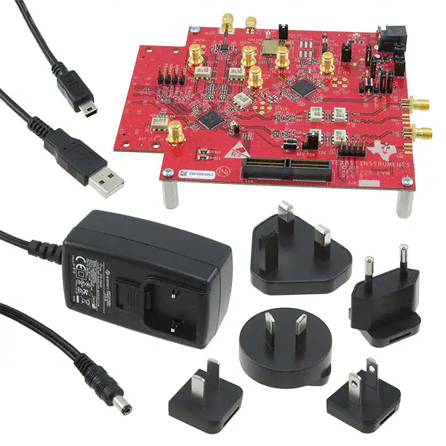
The fastest way to get the AFE722x EVM up and running is to follow this operating procedure:
• Two signal generators should be connected to the clock and data input of the EVM - preferably with
bandpass filter and 10-MHz reference locked for coherency.
• Clock input should be connected to CDC AUX IN input for AUX clock setup and the clock generator
amplitude should be set to ~10–13 dBm.
• TSW1400 or TSW1405 (RX) capture card should be plugged in to the AFE722x EVM and connected
to the PC via USB.
• TSW1400 or TSW1406 (TX) pattern generation card should be plugged into the AFE722x EVM and
connected to PC via Ethernet cable.
• All appropriate power supplies should be connected – blue LED (D2) on AFE722x EVM indicating
power good status.
• After performing USB reset in AFE722x EVM software, the flashing USB warning sign should
disappear indicating successful USB communication.
4
AFE722x Evaluation Module (AFE722xEVM) User's Guide
Copyright © 2013, Texas Instruments Incorporated
SLOU362 – February 2013
Submit Documentation Feedback
�Initial EVM Setup and Basic Test Procedure
www.ti.com
Figure 3. AFE722x EVM Setup
4.1
CDCE72010 Configuration
The initial EVM setup is configured so that the AFE722x can be operated at any desired sampling rate.
Since the TSW1400 requires an external clock at ¾ of the AFE clock rate (see clocking section) the
external clock applied to the CDC AUX IN connector needs to be 3× the AFE sampling rate (that is,
368.64 MHz for 122.88-MHz operation). Loading a preconfigured register file (AUX IN - div3 AFE div4
TSW.txt) to the CDCE72010, it then sets the dividers so that a /3 copy of the input clock is routed to the
AFE722x clock input and a /4 copy to the TSW1400.
Figure 4. CDCE72010 Configuration
4.2
RX Path Using TSW1400
First the AFE722x digital interface needs to be configured to match the serial LVDS interface that the
TSW1400 is expecting. The following control registers need to be set in the General Setup tab of the
AFE722x programming software. Also, the USB communication warning sign should be monitored after
the USB reset, to ensure proper communication with the AFE722x EVM.
SLOU362 – February 2013
Submit Documentation Feedback
AFE722x Evaluation Module (AFE722xEVM) User's Guide
Copyright © 2013, Texas Instruments Incorporated
5
�Initial EVM Setup and Basic Test Procedure
www.ti.com
Register Bit
Setting
Interface
Serial LVDS
Master Override
Enabled
Format
Offset Binary
Serial LVDS
2 Wire
Data Orientation
MSB First
SDR Mode
Disabled
Wordwise Output
Disabled
Bitwise RX
Disabled
Halfrx in 2wire
Disabled
The general setup tab includes
controls for the digital RX interface
The section controls the setup of the digital
interface as well as test modes and digital
features such as decimation and loopback
In the TSW1400 software, select the AFE722x as the ADC. Next, enter the sampling rate and ADC input
frequency and the TSW1400 software will calculate the coherent frequency.
Performing a capture should yield:
Fs = 122.88 Msps
Fin = 9.98625 MHz
6
AFE722x Evaluation Module (AFE722xEVM) User's Guide
Copyright © 2013, Texas Instruments Incorporated
SLOU362 – February 2013
Submit Documentation Feedback
�Initial EVM Setup and Basic Test Procedure
www.ti.com
Figure 5. HSDCP Settings
4.3
TX Path Using TSW1400
Configure the AFE722x digital interface to match the serial LVDS interface from the TSW1400.
In the General Setup tab of the AFE722x programming software, set the control registers as shown in
Table 1. Also, the USB communication warning sign should be monitored after the USB reset to ensure
proper communication with the AFE722x EVM.
Table 1. Control Registers
SLOU362 – February 2013
Submit Documentation Feedback
Register Bit
Setting
Interface
Serial LVDS
Master Override
Enabled
Serial LVDS
2 Wire
Data Orientation
MSB first
Format
2s Complement
Clock Delay
Enabled
Clock Delay
300 ps
Frame Clock Delay
Disabled
Frame Clock Delay
0 ps
AFE722x Evaluation Module (AFE722xEVM) User's Guide
Copyright © 2013, Texas Instruments Incorporated
7
�Initial EVM Setup and Basic Test Procedure
www.ti.com
The data coming from the TSW1400 is edge aligned while the AFE722x expects the serial LVDS data to
arrive edge centered. Here the programmable clock delay inside the AFE722x can be used to delay the
edge-aligned clock closer towards the center of the data.
DCLK
Data
Table 2 shows clock delays for DAC sampling rates that showed proper operation.
Table 2. Clock Delays for Listed DAC Sampling Rates
DAC Sampling Rate
Suitable Clock Delay
130 Msps
0 ps to 900 ps
122.88 Msps
0 ps to 900 ps
100 Msps
0 ps to 1.2 ns
80 Msps
0 ps to 1.8 ns
65 Msps
0 ps to 2.1 ns
40 Msps
0 ps to 2.1 ns
The general setup tab includes
controls for the digital TX interface
This section controls the setup of the digital
interface as well as the TX interpolation
Figure 6.
For TX, the output data of the TSW1400 needs to be properly configured for 6× serialization using High
Speed Data Converter Pro.
1. Install the latest High Speed Data Converter Pro GUI Installer from www.ti.com/tool/tsw1400evm
2. Open High Speed Data Converter Pro GUI
3. Enter Data Rate to DAC
4. Enter Tone BW, # and Tone Center frequency
5. Ensure match on data format between TSW1400 and AFE722x
8
AFE722x Evaluation Module (AFE722xEVM) User's Guide
Copyright © 2013, Texas Instruments Incorporated
SLOU362 – February 2013
Submit Documentation Feedback
�Initial EVM Setup and Basic Test Procedure
www.ti.com
6. Select Create Tones
7. Press the Send button
Figure 7.
The DAC output should show something like Figure 8 on the spectrum analyzer.
SLOU362 – February 2013
Submit Documentation Feedback
AFE722x Evaluation Module (AFE722xEVM) User's Guide
Copyright © 2013, Texas Instruments Incorporated
9
�Initial EVM Setup and Basic Test Procedure
www.ti.com
Figure 8. Spectrum Analyzer: Sample Rate = 245.76 Msps, Input Tone = 15 MHz
10
AFE722x Evaluation Module (AFE722xEVM) User's Guide
Copyright © 2013, Texas Instruments Incorporated
SLOU362 – February 2013
Submit Documentation Feedback
�Power Supply Options
www.ti.com
5
Power Supply Options
The AFE722x EVM is designed to operate from an external 6-V wall wart supply. An LDO generates a 5-V
rail for the TRF3703 IQ modulator as well as for the low-noise LDOs, which are generating a 3.3-V and
1.8-V rail for the AFE722x and the CDCE72010. Alternatively, the 3.3-V and 1.8-V rails can be generated
using DC/DC converters which operate directly from the 6-V input for maximum power efficiency.
The EVM provides options to disable unused circuits by means of pin headers. These headers can also
be used for accurate power measurements where external power supplies can be directly connected to
them.
Three pin headers allow a convenient change between powering the AFE722x and CDCE72010 either
from a DC/DC converter or low-noise LDO.
6V Input
LDO
TPS7A4501
JP10
5V
TRF3703
I/Q Mod
JP19
LDO
TPS79633
JP12
3.3V
JP18
CDCE72010
JP11
DC/DC
TPS62291
6V
JP4
VCXO
JP14
LDO
TPS79518
JP13
1.8V
AFE722x
JP20
DC/DC
TPS62231
Figure 9. Power Supply Jumper Settings
6
Clocking Configuration
The AFE722x EVM offers 3 different options for
providing the clock to the AFE722x as well as the
supporting circuitry. The biggest challenge arises
when using the DAC with the TSW1400 because
the TSW1400 expects an input clock at 1/8 of the
DAC input data rate. However, since the AFE722x
is designed for the serial LVDS interface, the DAC
data rate is 6x the actual AFE722x clock frequency.
Hence, the clock to the TSW1400 needs to 6/8 =
3/4x the AFE722x clock frequency.
SLOU362 – February 2013
Submit Documentation Feedback
AFE722x Evaluation Module (AFE722xEVM) User's Guide
Copyright © 2013, Texas Instruments Incorporated
11
�Clocking Configuration
www.ti.com
The CDCE72010 clock buffer on the AFE722x is used to provide the clock to the TSW1400. Additional
dividers can be added to the clock output in order to divide the clock appropriately for optional
interpolation by 2x or 4x.
Figure 10. Configuration of Clock Output in CDCE72010
Preconfigured setup files:
AUX IN – INT2x – div3 AFE div8
TSW.txt
AUX IN – div3 AFE div4 TSW.txt
REF IN (10MHz) – div6 AFE div8
TSW.txt
REF IN (10MHz) – INT2x – div6 AFE
div16 TSW.txt
REF IN (122.88MHz) – div6 AFE div8
TSW.txt
6.1
ext 3x clock to CDC AUX IN (see Section 6.5)
ext 3x clock to CDC AUX IN (see Section 6.1)
ext 10MHz clock on REF IN (see Section 6.2)
ext 10MHz clock on REF IN (see Section 6.2/Section 6.5)
ext 122.88MHz clock on REF IN
(see Section 6.2)
Non-VCXO Option (Default)
This setup is the default configuration and provides the
option to operate AFE722x and TSW1400 synchronous at
any arbitrary sampling rate without the use of a VCXO.
This setup is useful for testing the AFE722x at clock
frequencies where a VCXO is not immediately available.
12
AFE722x Evaluation Module (AFE722xEVM) User's Guide
Copyright © 2013, Texas Instruments Incorporated
SLOU362 – February 2013
Submit Documentation Feedback
�Clocking Configuration
www.ti.com
6.2
System Level
In this system configuration on the EVM a VCXO at 6x the
desired clock frequency is required – alternatively a
different VCXO frequency can be used and the internal
CDCE72010 dividers adjusted accordingly. An external
reference can be locked to the VCXO for coherency using
the CDCE72010. In this configuration the CDCE72010
provides a /6 copy of the VCXO to the AFE722x clock
input as well as a /8 copy to the TSW1400.
Also, the AFE722x EVM offers a placeholder for a surface
mount bandpass filter between the CDCE72010 and
AFE722x to limit the clock phase noise.
6.3
AFE722x
VCXO
CDCE72010
RX Only
When testing only the ADCs for maximum performance,
the EVM provides an option to connect an external clock
directly to the AFE, bypassing the CDCE72010. R74, R76
and R112 need to be modified from their default
configuration.
The DACs of the AFE can still be operated, however, the
TSW1400 can’t be used for data generation as no
feedback clock is provided to it.
This option provides the lowest possible jitter option when
combined with an external bandpass filter.
6.4
RX and TX Independent Clocking
The AFE722x supports an option to run the dual ADCs at
a different sampling rate than the dual DACs. With a few
resistor changes, the clocking circuitry on the AFE722x
EVM can be configured to support that feature. However,
in this scenario the CDCE72010 is bypassed and no clock
is routed back to the TSW1400. Hence an additional clock
needs to be provided and the CDCE72010 configured
with the appropriate output divider to match the AFE722x
DAC clock rate with the data rate from the TSW1400 (see
Section 6.1 and Section 6.2).
6.5
SMA
R112
R74
Connector 0S
0S
CLK IN
R76
DNI
SMA
Connector
CLK IN\
R79
DNI
R161
0S
R78
0S
R82
50S
T9
C56
DNI
CLK INP
CLK INN
AFE722x
0S
0S
Interpolation on the DAC
The AFE722x offers 2x and 4x interpolation of the DAC
output data. In order to employ interpolation on the DAC,
the clock going to the TSW1400 needs to be divided
accordingly. For example, interpolation by 2x in the DAC
requires that the data coming from the TSW1400 arrives
at ½ of the AFE722x clock frequency.
SLOU362 – February 2013
Submit Documentation Feedback
AFE722x Evaluation Module (AFE722xEVM) User's Guide
Copyright © 2013, Texas Instruments Incorporated
13
�RX Setup
6.6
www.ti.com
Decimation on the ADC
On the receive channels of the AFE722x, the output can be decimated by 2x using the on-chip FIR
halfband filter. This has no impact on the clock requirements to the AFE722x – it merely reduces the
output data rate by a factor of 2x and settings (sampling and input frequency) on the TSW1400 capture
card or other data capture tool need to be adjusted accordingly.
7
RX Setup
The RX section of the AFE722x is controlled on two
separate tabs of the EVM software.
In the ‘General Setup’ tab are the control registers for
the digital interface such as CMOS or serial LVDS
output, for example. In order to use the TSW1400 to
capture the received data, the following register settings
are required:
Register Bit
Interface
Master Override
Format
Serial LVDS
Data Orientation
DSR Mode
Wordwise Output
Bitwise RX
Halfrx in 2wire
Setting
Serial LVDS
Enabled
Offset Binary
2 Wire
MSB First
Disabled
Disabled
Disabled
Disabled
This tab also controls the register to set the digital
interface to test pattern mode and custom patterns can
be loaded as well. Furthermore RX decimation settings
as well as TX RX loopback mode are controlled here as
well.
14
The general setup tab includes
controls for the digital RX interface
The section controls the setup of the digital
interface as well as test modes and digital
features such as decimation and loopback
AFE722x Evaluation Module (AFE722xEVM) User's Guide
Copyright © 2013, Texas Instruments Incorporated
SLOU362 – February 2013
Submit Documentation Feedback
�TX Setup
www.ti.com
The other portion of the RX setup is located on the Receive Control tab which includes register access for
the mixing stage, power meter, and power options for the digital RX section. Also, the auxiliary ADC
registers are configured on this tab.
RX controls are
located on this tab
Mixing section controls gain, offset,
mixing mode and NCO
This section controls
power down options
on digital RX chain
The power meter
indicates the input
power level to the two
ADCs
This section controls
auxiliary ADC and its
mux input
Figure 11. Receive Control Tab in RX Setup
8
TX Setup
For the transmit output, the AFE722x EVM provides an option to directly route the DACs to SMA
connectors as well as an option to connect the dual DAC to an IQ modulator (TRF3703) for direct upconversion. shows the two options and the relevant 0Ω resistors to switch between them.
When using the IQ modulator, there is a separate SMA connector on the EVM for the LO input. Also there
is a low pass filter between DAC and IQ modulator for image suppression with a default cut off frequency
of 125 MHz.
SLOU362 – February 2013
Submit Documentation Feedback
AFE722x Evaluation Module (AFE722xEVM) User's Guide
Copyright © 2013, Texas Instruments Incorporated
15
�TX Setup
www.ti.com
R46 0S
SMA
Connector
DAC A
R56 0S
R127
DNI
R133
DNI
SMA
Connector
LO
Fc=125 MHz
TRF3703
RF Out
SMA
Connector
R114
DNI
R120
DNI
SMA
Connector
R58 0S
DAC B
R68 0S
Figure 12. AFE722x Schematic
When using the TSW1400 as a pattern generator for the AFE722x,
first the digital interface needs to be configured to match the serial
LVDS interface from the TSW1400.
The following control registers need to be set in the General Setup
tab of the AFE722x programming software.
The USB communication warning sign should also be monitored after
the USB reset to ensure proper communication with the AFE722x
EVM.
Register Bit
Interface
Master Override
Serial LVDS
Data Orientation
Format
Clock Delay
Clock Delay
Frame Clock Delay
Frame Clock Delay
16
Setting
Serial LVDS
Enabled
2 Wire
MSB First
2s Complement
Enabled
300 ps
Disabled
0 ps
AFE722x Evaluation Module (AFE722xEVM) User's Guide
Copyright © 2013, Texas Instruments Incorporated
SLOU362 – February 2013
Submit Documentation Feedback
�TX Setup
www.ti.com
The data coming from the TSW1400 is edge aligned while the
AFE722x expects the serial LVDS data to arrive edge centered. Here
the programmable clock delay can be used to delay the edge-aligned
clock closer towards the center of the data.
The table below shows clock delays for the listed DAC sampling rates
that showed proper operation:.
DAC Sampling Rate
130 Msps
122.88 Msps
100 Msps
80 Msps
65 Msps
40 Msps
DCLK
Data
Suitable Clock Delay
0 ps to 900 ps
0 ps to 900 ps
0 ps to 1.2 ns
0 ps to 1.8 ns
0 ps to 2.1 ns
0 ps to 2.1 ns
The other portion of the TX setup is located on the Transmit Control tab which includes register access for
the mixing stage, FIFO, Loopback and power options for the digital TX section. The auxiliary DAC
registers are also configured on this tab.
TX controls are
located on this tab
This section controls
the TX FIFO
Mixing section controls gain, offset,
mixing mode and NCO
This section controls
power down options
on digital TX chain
RX to TX Loopback
Enable
This section controls
auxiliary DACs
Figure 13. Transmit Control Tab in TX Setup
SLOU362 – February 2013
Submit Documentation Feedback
AFE722x Evaluation Module (AFE722xEVM) User's Guide
Copyright © 2013, Texas Instruments Incorporated
17
�EVALUATION BOARD/KIT/MODULE (EVM) ADDITIONAL TERMS
Texas Instruments (TI) provides the enclosed Evaluation Board/Kit/Module (EVM) under the following conditions:
The user assumes all responsibility and liability for proper and safe handling of the goods. Further, the user indemnifies TI from all claims
arising from the handling or use of the goods.
Should this evaluation board/kit not meet the specifications indicated in the User’s Guide, the board/kit may be returned within 30 days from
the date of delivery for a full refund. THE FOREGOING LIMITED WARRANTY IS THE EXCLUSIVE WARRANTY MADE BY SELLER TO
BUYER AND IS IN LIEU OF ALL OTHER WARRANTIES, EXPRESSED, IMPLIED, OR STATUTORY, INCLUDING ANY WARRANTY OF
MERCHANTABILITY OR FITNESS FOR ANY PARTICULAR PURPOSE. EXCEPT TO THE EXTENT OF THE INDEMNITY SET FORTH
ABOVE, NEITHER PARTY SHALL BE LIABLE TO THE OTHER FOR ANY INDIRECT, SPECIAL, INCIDENTAL, OR CONSEQUENTIAL
DAMAGES.
Please read the User's Guide and, specifically, the Warnings and Restrictions notice in the User's Guide prior to handling the product. This
notice contains important safety information about temperatures and voltages. For additional information on TI's environmental and/or safety
programs, please visit www.ti.com/esh or contact TI.
No license is granted under any patent right or other intellectual property right of TI covering or relating to any machine, process, or
combination in which such TI products or services might be or are used. TI currently deals with a variety of customers for products, and
therefore our arrangement with the user is not exclusive. TI assumes no liability for applications assistance, customer product design,
software performance, or infringement of patents or services described herein.
REGULATORY COMPLIANCE INFORMATION
As noted in the EVM User’s Guide and/or EVM itself, this EVM and/or accompanying hardware may or may not be subject to the Federal
Communications Commission (FCC) and Industry Canada (IC) rules.
For EVMs not subject to the above rules, this evaluation board/kit/module is intended for use for ENGINEERING DEVELOPMENT,
DEMONSTRATION OR EVALUATION PURPOSES ONLY and is not considered by TI to be a finished end product fit for general consumer
use. It generates, uses, and can radiate radio frequency energy and has not been tested for compliance with the limits of computing
devices pursuant to part 15 of FCC or ICES-003 rules, which are designed to provide reasonable protection against radio frequency
interference. Operation of the equipment may cause interference with radio communications, in which case the user at his own expense will
be required to take whatever measures may be required to correct this interference.
General Statement for EVMs including a radio
User Power/Frequency Use Obligations: This radio is intended for development/professional use only in legally allocated frequency and
power limits. Any use of radio frequencies and/or power availability of this EVM and its development application(s) must comply with local
laws governing radio spectrum allocation and power limits for this evaluation module. It is the user’s sole responsibility to only operate this
radio in legally acceptable frequency space and within legally mandated power limitations. Any exceptions to this are strictly prohibited and
unauthorized by Texas Instruments unless user has obtained appropriate experimental/development licenses from local regulatory
authorities, which is responsibility of user including its acceptable authorization.
For EVMs annotated as FCC – FEDERAL COMMUNICATIONS COMMISSION Part 15 Compliant
Caution
This device complies with part 15 of the FCC Rules. Operation is subject to the following two conditions: (1) This device may not cause
harmful interference, and (2) this device must accept any interference received, including interference that may cause undesired operation.
Changes or modifications not expressly approved by the party responsible for compliance could void the user's authority to operate the
equipment.
FCC Interference Statement for Class A EVM devices
This equipment has been tested and found to comply with the limits for a Class A digital device, pursuant to part 15 of the FCC Rules.
These limits are designed to provide reasonable protection against harmful interference when the equipment is operated in a commercial
environment. This equipment generates, uses, and can radiate radio frequency energy and, if not installed and used in accordance with the
instruction manual, may cause harmful interference to radio communications. Operation of this equipment in a residential area is likely to
cause harmful interference in which case the user will be required to correct the interference at his own expense.
�FCC Interference Statement for Class B EVM devices
This equipment has been tested and found to comply with the limits for a Class B digital device, pursuant to part 15 of the FCC Rules.
These limits are designed to provide reasonable protection against harmful interference in a residential installation. This equipment
generates, uses and can radiate radio frequency energy and, if not installed and used in accordance with the instructions, may cause
harmful interference to radio communications. However, there is no guarantee that interference will not occur in a particular installation. If
this equipment does cause harmful interference to radio or television reception, which can be determined by turning the equipment off and
on, the user is encouraged to try to correct the interference by one or more of the following measures:
• Reorient or relocate the receiving antenna.
• Increase the separation between the equipment and receiver.
• Connect the equipment into an outlet on a circuit different from that to which the receiver is connected.
• Consult the dealer or an experienced radio/TV technician for help.
For EVMs annotated as IC – INDUSTRY CANADA Compliant
This Class A or B digital apparatus complies with Canadian ICES-003.
Changes or modifications not expressly approved by the party responsible for compliance could void the user’s authority to operate the
equipment.
Concerning EVMs including radio transmitters
This device complies with Industry Canada licence-exempt RSS standard(s). Operation is subject to the following two conditions: (1) this
device may not cause interference, and (2) this device must accept any interference, including interference that may cause undesired
operation of the device.
Concerning EVMs including detachable antennas
Under Industry Canada regulations, this radio transmitter may only operate using an antenna of a type and maximum (or lesser) gain
approved for the transmitter by Industry Canada. To reduce potential radio interference to other users, the antenna type and its gain should
be so chosen that the equivalent isotropically radiated power (e.i.r.p.) is not more than that necessary for successful communication.
This radio transmitter has been approved by Industry Canada to operate with the antenna types listed in the user guide with the maximum
permissible gain and required antenna impedance for each antenna type indicated. Antenna types not included in this list, having a gain
greater than the maximum gain indicated for that type, are strictly prohibited for use with this device.
Cet appareil numérique de la classe A ou B est conforme à la norme NMB-003 du Canada.
Les changements ou les modifications pas expressément approuvés par la partie responsable de la conformité ont pu vider l’autorité de
l'utilisateur pour actionner l'équipement.
Concernant les EVMs avec appareils radio
Le présent appareil est conforme aux CNR d'Industrie Canada applicables aux appareils radio exempts de licence. L'exploitation est
autorisée aux deux conditions suivantes : (1) l'appareil ne doit pas produire de brouillage, et (2) l'utilisateur de l'appareil doit accepter tout
brouillage radioélectrique subi, même si le brouillage est susceptible d'en compromettre le fonctionnement.
Concernant les EVMs avec antennes détachables
Conformément à la réglementation d'Industrie Canada, le présent émetteur radio peut fonctionner avec une antenne d'un type et d'un gain
maximal (ou inférieur) approuvé pour l'émetteur par Industrie Canada. Dans le but de réduire les risques de brouillage radioélectrique à
l'intention des autres utilisateurs, il faut choisir le type d'antenne et son gain de sorte que la puissance isotrope rayonnée équivalente
(p.i.r.e.) ne dépasse pas l'intensité nécessaire à l'établissement d'une communication satisfaisante.
Le présent émetteur radio a été approuvé par Industrie Canada pour fonctionner avec les types d'antenne énumérés dans le manuel
d’usage et ayant un gain admissible maximal et l'impédance requise pour chaque type d'antenne. Les types d'antenne non inclus dans
cette liste, ou dont le gain est supérieur au gain maximal indiqué, sont strictement interdits pour l'exploitation de l'émetteur.
SPACER
SPACER
SPACER
SPACER
SPACER
SPACER
SPACER
SPACER
�【Important Notice for Users of this Product in Japan】
】
This development kit is NOT certified as Confirming to Technical Regulations of Radio Law of Japan
If you use this product in Japan, you are required by Radio Law of Japan to follow the instructions below with respect to this product:
1.
2.
3.
Use this product in a shielded room or any other test facility as defined in the notification #173 issued by Ministry of Internal Affairs and
Communications on March 28, 2006, based on Sub-section 1.1 of Article 6 of the Ministry’s Rule for Enforcement of Radio Law of
Japan,
Use this product only after you obtained the license of Test Radio Station as provided in Radio Law of Japan with respect to this
product, or
Use of this product only after you obtained the Technical Regulations Conformity Certification as provided in Radio Law of Japan with
respect to this product. Also, please do not transfer this product, unless you give the same notice above to the transferee. Please note
that if you could not follow the instructions above, you will be subject to penalties of Radio Law of Japan.
Texas Instruments Japan Limited
(address) 24-1, Nishi-Shinjuku 6 chome, Shinjuku-ku, Tokyo, Japan
http://www.tij.co.jp
【ご使用にあたっての注】
本開発キットは技術基準適合証明を受けておりません。
本製品のご使用に際しては、電波法遵守のため、以下のいずれかの措置を取っていただく必要がありますのでご注意ください。
1.
2.
3.
電波法施行規則第6条第1項第1号に基づく平成18年3月28日総務省告示第173号で定められた電波暗室等の試験設備でご使用いただく。
実験局の免許を取得後ご使用いただく。
技術基準適合証明を取得後ご使用いただく。
なお、本製品は、上記の「ご使用にあたっての注意」を譲渡先、移転先に通知しない限り、譲渡、移転できないものとします。
上記を遵守頂けない場合は、電波法の罰則が適用される可能性があることをご留意ください。
日本テキサス・インスツルメンツ株式会社
東京都新宿区西新宿6丁目24番1号
西新宿三井ビル
http://www.tij.co.jp
SPACER
SPACER
SPACER
SPACER
SPACER
SPACER
SPACER
SPACER
SPACER
SPACER
SPACER
SPACER
SPACER
SPACER
SPACER
SPACER
�EVALUATION BOARD/KIT/MODULE (EVM)
WARNINGS, RESTRICTIONS AND DISCLAIMERS
For Feasibility Evaluation Only, in Laboratory/Development Environments. Unless otherwise indicated, this EVM is not a finished
electrical equipment and not intended for consumer use. It is intended solely for use for preliminary feasibility evaluation in
laboratory/development environments by technically qualified electronics experts who are familiar with the dangers and application risks
associated with handling electrical mechanical components, systems and subsystems. It should not be used as all or part of a finished end
product.
Your Sole Responsibility and Risk. You acknowledge, represent and agree that:
1.
2.
3.
4.
You have unique knowledge concerning Federal, State and local regulatory requirements (including but not limited to Food and Drug
Administration regulations, if applicable) which relate to your products and which relate to your use (and/or that of your employees,
affiliates, contractors or designees) of the EVM for evaluation, testing and other purposes.
You have full and exclusive responsibility to assure the safety and compliance of your products with all such laws and other applicable
regulatory requirements, and also to assure the safety of any activities to be conducted by you and/or your employees, affiliates,
contractors or designees, using the EVM. Further, you are responsible to assure that any interfaces (electronic and/or mechanical)
between the EVM and any human body are designed with suitable isolation and means to safely limit accessible leakage currents to
minimize the risk of electrical shock hazard.
You will employ reasonable safeguards to ensure that your use of the EVM will not result in any property damage, injury or death, even
if the EVM should fail to perform as described or expected.
You will take care of proper disposal and recycling of the EVM’s electronic components and packing materials.
Certain Instructions. It is important to operate this EVM within TI’s recommended specifications and environmental considerations per the
user guidelines. Exceeding the specified EVM ratings (including but not limited to input and output voltage, current, power, and
environmental ranges) may cause property damage, personal injury or death. If there are questions concerning these ratings please contact
a TI field representative prior to connecting interface electronics including input power and intended loads. Any loads applied outside of the
specified output range may result in unintended and/or inaccurate operation and/or possible permanent damage to the EVM and/or
interface electronics. Please consult the EVM User's Guide prior to connecting any load to the EVM output. If there is uncertainty as to the
load specification, please contact a TI field representative. During normal operation, some circuit components may have case temperatures
greater than 60°C as long as the input and output are maintained at a normal ambient operating temperature. These components include
but are not limited to linear regulators, switching transistors, pass transistors, and current sense resistors which can be identified using the
EVM schematic located in the EVM User's Guide. When placing measurement probes near these devices during normal operation, please
be aware that these devices may be very warm to the touch. As with all electronic evaluation tools, only qualified personnel knowledgeable
in electronic measurement and diagnostics normally found in development environments should use these EVMs.
Agreement to Defend, Indemnify and Hold Harmless. You agree to defend, indemnify and hold TI, its licensors and their representatives
harmless from and against any and all claims, damages, losses, expenses, costs and liabilities (collectively, "Claims") arising out of or in
connection with any use of the EVM that is not in accordance with the terms of the agreement. This obligation shall apply whether Claims
arise under law of tort or contract or any other legal theory, and even if the EVM fails to perform as described or expected.
Safety-Critical or Life-Critical Applications. If you intend to evaluate the components for possible use in safety critical applications (such
as life support) where a failure of the TI product would reasonably be expected to cause severe personal injury or death, such as devices
which are classified as FDA Class III or similar classification, then you must specifically notify TI of such intent and enter into a separate
Assurance and Indemnity Agreement.
Mailing Address: Texas Instruments, Post Office Box 655303, Dallas, Texas 75265
Copyright © 2012, Texas Instruments Incorporated
�IMPORTANT NOTICE
Texas Instruments Incorporated and its subsidiaries (TI) reserve the right to make corrections, enhancements, improvements and other
changes to its semiconductor products and services per JESD46, latest issue, and to discontinue any product or service per JESD48, latest
issue. Buyers should obtain the latest relevant information before placing orders and should verify that such information is current and
complete. All semiconductor products (also referred to herein as “components”) are sold subject to TI’s terms and conditions of sale
supplied at the time of order acknowledgment.
TI warrants performance of its components to the specifications applicable at the time of sale, in accordance with the warranty in TI’s terms
and conditions of sale of semiconductor products. Testing and other quality control techniques are used to the extent TI deems necessary
to support this warranty. Except where mandated by applicable law, testing of all parameters of each component is not necessarily
performed.
TI assumes no liability for applications assistance or the design of Buyers’ products. Buyers are responsible for their products and
applications using TI components. To minimize the risks associated with Buyers’ products and applications, Buyers should provide
adequate design and operating safeguards.
TI does not warrant or represent that any license, either express or implied, is granted under any patent right, copyright, mask work right, or
other intellectual property right relating to any combination, machine, or process in which TI components or services are used. Information
published by TI regarding third-party products or services does not constitute a license to use such products or services or a warranty or
endorsement thereof. Use of such information may require a license from a third party under the patents or other intellectual property of the
third party, or a license from TI under the patents or other intellectual property of TI.
Reproduction of significant portions of TI information in TI data books or data sheets is permissible only if reproduction is without alteration
and is accompanied by all associated warranties, conditions, limitations, and notices. TI is not responsible or liable for such altered
documentation. Information of third parties may be subject to additional restrictions.
Resale of TI components or services with statements different from or beyond the parameters stated by TI for that component or service
voids all express and any implied warranties for the associated TI component or service and is an unfair and deceptive business practice.
TI is not responsible or liable for any such statements.
Buyer acknowledges and agrees that it is solely responsible for compliance with all legal, regulatory and safety-related requirements
concerning its products, and any use of TI components in its applications, notwithstanding any applications-related information or support
that may be provided by TI. Buyer represents and agrees that it has all the necessary expertise to create and implement safeguards which
anticipate dangerous consequences of failures, monitor failures and their consequences, lessen the likelihood of failures that might cause
harm and take appropriate remedial actions. Buyer will fully indemnify TI and its representatives against any damages arising out of the use
of any TI components in safety-critical applications.
In some cases, TI components may be promoted specifically to facilitate safety-related applications. With such components, TI’s goal is to
help enable customers to design and create their own end-product solutions that meet applicable functional safety standards and
requirements. Nonetheless, such components are subject to these terms.
No TI components are authorized for use in FDA Class III (or similar life-critical medical equipment) unless authorized officers of the parties
have executed a special agreement specifically governing such use.
Only those TI components which TI has specifically designated as military grade or “enhanced plastic” are designed and intended for use in
military/aerospace applications or environments. Buyer acknowledges and agrees that any military or aerospace use of TI components
which have not been so designated is solely at the Buyer's risk, and that Buyer is solely responsible for compliance with all legal and
regulatory requirements in connection with such use.
TI has specifically designated certain components as meeting ISO/TS16949 requirements, mainly for automotive use. In any case of use of
non-designated products, TI will not be responsible for any failure to meet ISO/TS16949.
Products
Applications
Audio
www.ti.com/audio
Automotive and Transportation
www.ti.com/automotive
Amplifiers
amplifier.ti.com
Communications and Telecom
www.ti.com/communications
Data Converters
dataconverter.ti.com
Computers and Peripherals
www.ti.com/computers
DLP® Products
www.dlp.com
Consumer Electronics
www.ti.com/consumer-apps
DSP
dsp.ti.com
Energy and Lighting
www.ti.com/energy
Clocks and Timers
www.ti.com/clocks
Industrial
www.ti.com/industrial
Interface
interface.ti.com
Medical
www.ti.com/medical
Logic
logic.ti.com
Security
www.ti.com/security
Power Mgmt
power.ti.com
Space, Avionics and Defense
www.ti.com/space-avionics-defense
Microcontrollers
microcontroller.ti.com
Video and Imaging
www.ti.com/video
RFID
www.ti-rfid.com
OMAP Applications Processors
www.ti.com/omap
TI E2E Community
e2e.ti.com
Wireless Connectivity
www.ti.com/wirelessconnectivity
Mailing Address: Texas Instruments, Post Office Box 655303, Dallas, Texas 75265
Copyright © 2013, Texas Instruments Incorporated
�