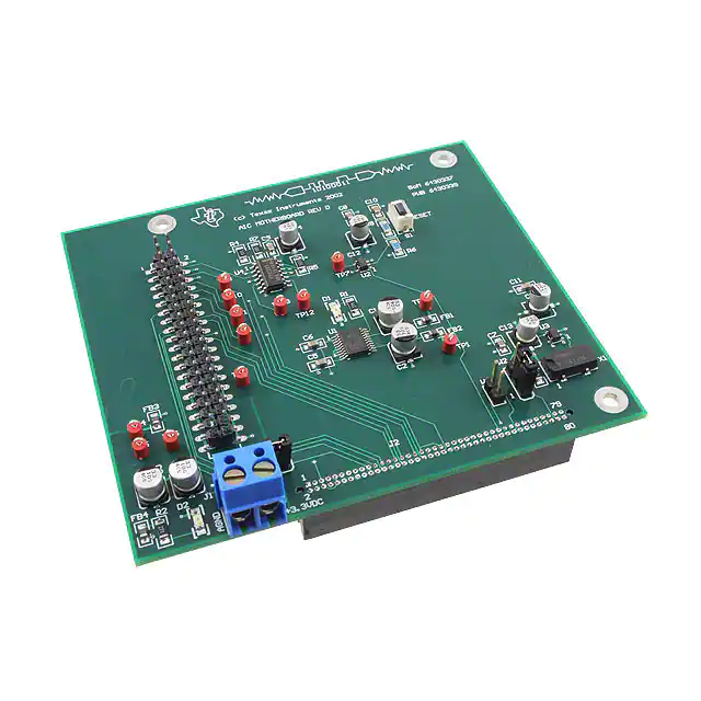
DSP−Codec Development
Platform
User’s Guide
September 2002
Data Acquisition Products
SLAU090
�IMPORTANT NOTICE
Texas Instruments Incorporated and its subsidiaries (TI) reserve the right to make corrections, modifications,
enhancements, improvements, and other changes to its products and services at any time and to discontinue
any product or service without notice. Customers should obtain the latest relevant information before placing
orders and should verify that such information is current and complete. All products are sold subject to TI’s terms
and conditions of sale supplied at the time of order acknowledgment.
TI warrants performance of its hardware products to the specifications applicable at the time of sale in
accordance with TI’s standard warranty. Testing and other quality control techniques are used to the extent TI
deems necessary to support this warranty. Except where mandated by government requirements, testing of all
parameters of each product is not necessarily performed.
TI assumes no liability for applications assistance or customer product design. Customers are responsible for
their products and applications using TI components. To minimize the risks associated with customer products
and applications, customers should provide adequate design and operating safeguards.
TI does not warrant or represent that any license, either express or implied, is granted under any TI patent right,
copyright, mask work right, or other TI intellectual property right relating to any combination, machine, or process
in which TI products or services are used. Information published by TI regarding third-party products or services
does not constitute a license from TI to use such products or services or a warranty or endorsement thereof.
Use of such information may require a license from a third party under the patents or other intellectual property
of the third party, or a license from TI under the patents or other intellectual property of TI.
Reproduction of information in TI data books or data sheets is permissible only if reproduction is without
alteration and is accompanied by all associated warranties, conditions, limitations, and notices. Reproduction
of this information with alteration is an unfair and deceptive business practice. TI is not responsible or liable for
such altered documentation.
Resale of TI products or services with statements different from or beyond the parameters stated by TI for that
product or service voids all express and any implied warranties for the associated TI product or service and
is an unfair and deceptive business practice. TI is not responsible or liable for any such statements.
Mailing Address:
Texas Instruments
Post Office Box 655303
Dallas, Texas 75265
Copyright 2002, Texas Instruments Incorporated
�EVM IMPORTANT NOTICE
Texas Instruments (TI) provides the enclosed product(s) under the following conditions:
This evaluation kit being sold by TI is intended for use for ENGINEERING DEVELOPMENT OR EVALUATION
PURPOSES ONLY and is not considered by TI to be fit for commercial use. As such, the goods being provided
may not be complete in terms of required design-, marketing-, and/or manufacturing-related protective
considerations, including product safety measures typically found in the end product incorporating the goods.
As a prototype, this product does not fall within the scope of the European Union directive on electromagnetic
compatibility and therefore may not meet the technical requirements of the directive.
Should this evaluation kit not meet the specifications indicated in the EVM User’s Guide, the kit may be returned
within 30 days from the date of delivery for a full refund. THE FOREGOING WARRANTY IS THE EXCLUSIVE
WARRANTY MADE BY SELLER TO BUYER AND IS IN LIEU OF ALL OTHER WARRANTIES, EXPRESSED,
IMPLIED, OR STATUTORY, INCLUDING ANY WARRANTY OF MERCHANTABILITY OR FITNESS FOR ANY
PARTICULAR PURPOSE.
The user assumes all responsibility and liability for proper and safe handling of the goods. Further, the user
indemnifies TI from all claims arising from the handling or use of the goods. Please be aware that the products
received may not be regulatory compliant or agency certified (FCC, UL, CE, etc.). Due to the open construction
of the product, it is the user’s responsibility to take any and all appropriate precautions with regard to electrostatic
discharge.
EXCEPT TO THE EXTENT OF THE INDEMNITY SET FORTH ABOVE, NEITHER PARTY SHALL BE LIABLE
TO THE OTHER FOR ANY INDIRECT, SPECIAL, INCIDENTAL, OR CONSEQUENTIAL DAMAGES.
TI currently deals with a variety of customers for products, and therefore our arrangement with the user is not
exclusive.
TI assumes no liability for applications assistance, customer product design, software performance, or
infringement of patents or services described herein.
Please read the EVM User’s Guide and, specifically, the EVM Warnings and Restrictions notice in the EVM
User’s Guide prior to handling the product. This notice contains important safety information about temperatures
and voltages. For further safety concerns, please contact the TI application engineer.
Persons handling the product must have electronics training and observe good laboratory practice standards.
No license is granted under any patent right or other intellectual property right of TI covering or relating to any
machine, process, or combination in which such TI products or services might be or are used.
Mailing Address:
Texas Instruments
Post Office Box 655303
Dallas, Texas 75265
Copyright 2002, Texas Instruments Incorporated
�EVM WARNINGS AND RESTRICTIONS
It is important to operate this EVM within the input voltage range of 3.3 V described in the EVM
User’s Guide.
Exceeding the specified input range may cause unexpected operation and/or irreversible
damage to the EVM. If there are questions concerning the input range, please contact a TI
field representative prior to connecting the input power.
Applying loads outside of the specified output range may result in unintended operation and/or
possible permanent damage to the EVM. Please consult the EVM User’s Guide prior to
connecting any load to the EVM output. If there is uncertainty as to the load specification,
please contact a TI field representative.
During normal operation, some circuit components may have case temperatures greater than
60°C. The EVM is designed to operate properly with certain components above 60°C as long
as the input and output ranges are maintained. These components include but are not limited
to linear regulators, switching transistors, pass transistors, and current sense resistors. These
types of devices can be identified using the EVM schematic located in the EVM User’s Guide.
When placing measurement probes near these devices during operation, please be aware
that these devices may be very warm to the touch.
Mailing Address:
Texas Instruments
Post Office Box 655303
Dallas, Texas 75265
Copyright 2002, Texas Instruments Incorporated
�Related Documentation From Texas Instruments
Preface
Read This First
About This Manual
This user’s guide describes the operation and use of the DSP-codec
development platform. A complete circuit description as well as schematic
diagram and bill of materials are also included.
How to Use This Manual
This document contains the following chapters:
- Chapter 1 – Introduction and EVM Overview
- Chapter 2 – Digital Interface
- Chapter 3 – Support Functions
- Chapter 4 – EVM Bill of Materials and Schematic
Related Documentation From Texas Instruments
To obtain a copy of any of the following TI documents, call the Texas
Instruments literature response center at (800) 477-8924 or the product
information center (PIC) at (972) 644-5580. When ordering, please identify
this booklet by its title and literature number. Updated documents can also be
obtained through the TI website at www.ti.com.
Data Sheets:
Literature Number:
SN74LVC1G08DBVR
SN74LVC74ADR
SCES217J
SCAS287M
TPS70151PWP
SLVS222A
v
�Contents
FCC Warning
This equipment is intended for use in a laboratory test environment only. It
generates, uses, and can radiate radio frequency energy and has not been
tested for compliance with the limits of computing devices pursuant to subpart
J of part 15 of FCC rules, which are designed to provide reasonable protection
against radio frequency interference. Operation of this equipment in other
environments may cause interference with radio communications, in which
case the user at his own expense will be required to take whatever measures
may be required to correct this interference.
vi
�Contents
Contents
1
Introduction and EVM Overview . . . . . . . . . . . . . . . . . . . . . . . . . . . . . . . . . . . . . . . . . . . . . . . . . . 1-1
1.1
Features . . . . . . . . . . . . . . . . . . . . . . . . . . . . . . . . . . . . . . . . . . . . . . . . . . . . . . . . . . . . . . . . . . 1-2
1.2
Introduction . . . . . . . . . . . . . . . . . . . . . . . . . . . . . . . . . . . . . . . . . . . . . . . . . . . . . . . . . . . . . . . . 1-2
2
Digital Interface . . . . . . . . . . . . . . . . . . . . . . . . . . . . . . . . . . . . . . . . . . . . . . . . . . . . . . . . . . . . . . . . .
2.1
Introduciton . . . . . . . . . . . . . . . . . . . . . . . . . . . . . . . . . . . . . . . . . . . . . . . . . . . . . . . . . . . . . . . .
2.2
DSP-to-Platform . . . . . . . . . . . . . . . . . . . . . . . . . . . . . . . . . . . . . . . . . . . . . . . . . . . . . . . . . . . .
2.3
Platform-to-Codec . . . . . . . . . . . . . . . . . . . . . . . . . . . . . . . . . . . . . . . . . . . . . . . . . . . . . . . . . .
2-1
2-2
2-3
2-3
3
Support Functions . . . . . . . . . . . . . . . . . . . . . . . . . . . . . . . . . . . . . . . . . . . . . . . . . . . . . . . . . . . . . . .
3.1
Introduction . . . . . . . . . . . . . . . . . . . . . . . . . . . . . . . . . . . . . . . . . . . . . . . . . . . . . . . . . . . . . . . .
3.1.1 MCLK Generation . . . . . . . . . . . . . . . . . . . . . . . . . . . . . . . . . . . . . . . . . . . . . . . . . . .
3.1.2 Reset Generation . . . . . . . . . . . . . . . . . . . . . . . . . . . . . . . . . . . . . . . . . . . . . . . . . . . .
3.1.3 Power Options . . . . . . . . . . . . . . . . . . . . . . . . . . . . . . . . . . . . . . . . . . . . . . . . . . . . . .
3.2
Key Signal Synchronization . . . . . . . . . . . . . . . . . . . . . . . . . . . . . . . . . . . . . . . . . . . . . . . . . .
3-1
3-2
3-2
3-2
3-2
3-3
4
EVM Bill of Materials and Schematic . . . . . . . . . . . . . . . . . . . . . . . . . . . . . . . . . . . . . . . . . . . . . . 4-1
4.1
EVM Bill of Materials . . . . . . . . . . . . . . . . . . . . . . . . . . . . . . . . . . . . . . . . . . . . . . . . . . . . . . . . 4-2
4.2
EVM Schematic . . . . . . . . . . . . . . . . . . . . . . . . . . . . . . . . . . . . . . . . . . . . . . . . . . . . . . . . . . . . 4-2
Figures
2-1
DSP-Codec Development Platform . . . . . . . . . . . . . . . . . . . . . . . . . . . . . . . . . . . . . . . . . . . . . . 2-2
Tables
2-1
3-1
3-2
J2 Connector Pinouts . . . . . . . . . . . . . . . . . . . . . . . . . . . . . . . . . . . . . . . . . . . . . . . . . . . . . . . . . . 2-3
Jumper W2 Function . . . . . . . . . . . . . . . . . . . . . . . . . . . . . . . . . . . . . . . . . . . . . . . . . . . . . . . . . . 3-2
Jumper W1 Function . . . . . . . . . . . . . . . . . . . . . . . . . . . . . . . . . . . . . . . . . . . . . . . . . . . . . . . . . . 3-2
vii
�Contents
viii
�Chapter 1
Introduction and EVM Overview
This chapter provides a brief overview of the DSP-codec development platform.
Topic
Page
1.1
Features . . . . . . . . . . . . . . . . . . . . . . . . . . . . . . . . . . . . . . . . . . . . . . . . . . . . . 1-2
1.2
Introduction . . . . . . . . . . . . . . . . . . . . . . . . . . . . . . . . . . . . . . . . . . . . . . . . . . 1-2
Introduction and EVM Overview
1-1
�Features
1.1 Features
- Provides all necessary voltages for device under test
- Provides bit clock for codecs
- Flexible interface to popular TI DSPs
- General codec requirements are addressed
1.2 Introduction
The DSP-codec development platform provides all the supplementary control
signals necessary to interface a range of TI codecs to TI DSP starter kits
(DSKs).
The platform supports the following devices
- TLV320AIC1103
- TLV320AIC1106
- TLV320AIC1107
- TLV320AIC1109
- TLV320AIC1110
- TLV320AIC12
- TLV320AIC13
- TLV320AIC14
- TLV320AIC15
- TLV320AIC20
- TLV320AIC21
- TLV320AIC22
- TLV320AIC24
1-2
�Chapter 2
Digital Interface
This chapter describes the digital interface of the DSP-codec development
platform.
Topic
Page
2.1
Introduction . . . . . . . . . . . . . . . . . . . . . . . . . . . . . . . . . . . . . . . . . . . . . . . . . . 2-2
2.2
DSP-to-Platform . . . . . . . . . . . . . . . . . . . . . . . . . . . . . . . . . . . . . . . . . . . . . . 2-3
2.3
Platform-to-Codec . . . . . . . . . . . . . . . . . . . . . . . . . . . . . . . . . . . . . . . . . . . . 2-3
Digital Interface
2-1
�Introduciton
2.1 Introduciton
There are two sections within the digital interface of the development platform:
- DSP-to-platform
- Platform-to-codec
Figure 2-1. DSP-Codec Development Platform
40 Pin Connector
Is Assembled Onto
the Top Side of
Board and Mates
With Various Codecs
80 Pin DSK
Connector Is
Assembled Onto the
Bottom Side of Bosrd
and Mates With DSK
2-2
�DSP-to-Platform
2.2 DSP-to-Platform
The development platform mates with TI DSKs via the 80-pin Samtec
connector located at J2. Consult the schematic for pinout details.
2.3 Platform-to-Codec
Codec EVMs mate with the development platform via a 40-pin Samtec
connector located at J3. The mating connector (Samtec part number,
SSW-120-22-F-D-VS-K)
is used on the EVM board to provide the electrical
connections necessary for various codec EVMs. Consult Samtec at
www.samtec.com or 1-800-SAMTEC-9 for more information.
The pinout for the 40-pin connector is given in Table 2-1.
Table 2-1. J2 Connector Pinouts
Pin Number
J2.1
Signal
MCLK
Description
Master clock
J2.2
J2.3
DGND
SCLK
Digital ground
Serial data clock
J2.4
J2.5
DGND
DIN
Digital ground
Data in
J2.6
J2.7
DGND
DOUT
Digital ground
Data out
J2.8
J2.9
Reserved
FS
Reserved for future use
Frame sync
J2.10
J2.11
Reserved
CLKX
Reserved for future use
Transmit clock
J2.12
J2.13
Reserved
FSX
Reserved for future use
Frame sync transmit
J2.14
J2.15
Reserved
DX
Reserved for future use
Data transmit
J2.16
J2.17
J2.18
DR
RESET
FSR
Data receive
Global reset for all devices
Frame sync receive
J2.19
J2.20
PWDN
CLKR
Global power down for all devices
Receive clock
J2.21
J2.22
CNTLb
CNTLa
GPIO pin
GPIO pin
J2.23
J2.24
STATb
STATa
Status pin
Status pin
J2.25
J2.26
3.3V_D
Reserved
Digital 3.3 V
Reserved for future use
J2.27
J2.28
3.3V_D
DGND
Digital 3.3 V
Digital ground
J2.29
J2.30
1.8V_D
DGND
Digital 1.8 V
Digital ground
J2.31
1.8V_D
Digital 1.8 V
Digital Interface
2-3
�Platform-to-Codec
Table 2-1. J2 Connector Pinouts (Continued)
2-4
Pin Number
J2.32
Signal
DGND
Description
Digital ground
J2.33
J2.34
3.3V_A_DRV
AGND
Output driver supply 3.3 V
Analog ground
J2.35
J2.36
3.3V_A_DRV
AGND
Output driver supply 3.3 V
Analog ground
J2.37
J2.38
3.3V_A
AGND
Analog 3.3 V
Analog ground
J2.39
J2.40
3.3V_A
AGND
Analog 3.3 V
Analog ground
�Chapter 3
Support Functions
This chapter provides a description of the codec support functions.
Topic
Page
3.1
Introduction . . . . . . . . . . . . . . . . . . . . . . . . . . . . . . . . . . . . . . . . . . . . . . . . . . 3-2
3.2
Key Signal Synchronization . . . . . . . . . . . . . . . . . . . . . . . . . . . . . . . . . . . . 3-3
Support Functions
3-1
�Introduction
3.1 Introduction
The development platform supports a number of functions required by the
codecs:
- MCLK generation
- Reset generation
- Power options
Alternatives for each function are described below.
3.1.1
MCLK Generation
MCLK is the clock required by the Sigma Delta converter. All other timing is
derived from MCLK. The DSK provides a clock that can be used as MCLK for
the codecs. Alternatively, a 100 MHz clock is available on the development
platform. Jumper W2 selects the clock source.
Table 3-1. Jumper W2 Function
Position
3.1.2
Function
1-2
DSP Clock is selected
2-3
100 MHz clock from development platform is selected
Reset Generation
Reset may be generated by either the DSK via software, or manually by
momentarily pressing SW1. Either of these options is valid and generates a
RESET signal that is asynchronous to MCLK.
3.1.3
Power Options
System power may be supplied from either the DSK via connector J2, or an
external source via connector J1. If an external source is used to supply
system power, switch the position of jumper W1.
Table 3-2. Jumper W1 Function
Position
3-2
W1 Function
1-2
3.3 V is supplied via the DSK
2-3
3.3 V is supplied via the J1 screw terminals
�Key Signal Synchronization
3.2 Key Signal Synchronization
The reset and power-down signals must be synchronized to MCLK before
being applied to any codec. As mentioned previously, RESET is generated by
the DSK or the user, and is asynchronous to the MCLK. Synchronization is
achieved by D-type flip-flop. Similarly, the PWDN signal is generated by the
user’s software, and is asynchronous to the MCLK signal. Synchronization of
PWDN is also achieved by D-type flip-flop.
Support Functions
3-3
�3-4
�Chapter 4
EVM Bill of Materials and Schematic
The development platform bill of materials and schematic are provided in this
chapter.
Topic
Page
4.1
EVM Bill of Materials . . . . . . . . . . . . . . . . . . . . . . . . . . . . . . . . . . . . . . . . . . 4-2
4.2
EVM Schematic . . . . . . . . . . . . . . . . . . . . . . . . . . . . . . . . . . . . . . . . . . . . . . . 4-2
EVM Bill of Materials and Schematic
4-1
�EVM Bill of Materials
4.1 EVM Bill of Materials
The following table contains a complete bill of materials for the DSP-codec
development platform. The schematic diagram is also provided for reference.
Contact the product information center, or e-mail dataconvapps@list.ti.com if
you have questions regarding this EVM.
Ref Des
Description
Vendor
Part number
C7, C8, C9, C10,
C11
Capacitor, 0.1 µF 50 V, ceramic
X7R 0805
Panasonic
ECJ-2YB1H104K
C5, C6
Capacitor, .22 µF 16 V ceramic X7R Panasonic
0805
ECJ-2VB1C224K
C12, C13, C14, C15
Capacitor, 10 µF 16 V
VS electrolytic SMD
Panasonic
ECE-V1CA100SR
C1, C2, C3, C4
Capacitor, 33 µF 10 V
VS electrolytic SMD
Panasonic
ECE-V1AA330SR
FairRite
2744044447
FB1, FB2, FB3, FB4, Ferrite bead inductor
FB5
R1, R2
RES 270 Ω 1/8 W 5%, 1206 SMD
Panasonic
ERJ-8GEYJ271V
R8
RES 1.0 kΩ 1/8 W,5%, 1206 SMD
Panasonic
ERJ-8GEYJ102V
R3, R4, R5
Resistor 10 kΩ, 1/8 W 5%, 1206
SMD
Panasonic
ERJ-8GEYJ103V
R6
Resistor 130 kΩ, 1/8 W 5% 1206
SMD
Panasonic
ERJ-8GEYJ134V
D1, D2
LED, green, clear 1206 SMD
Chicago Miniature
Lamp Inc
CMD5-21VGC/TR8
X1
100 MHz Oscillator
Epson
SG-8002JC100M-PCC
R7
TLV320 AIC motherboard
6430339
TLV320 AIC motherboard DDB
Texas Instruments
6430338
U2, U3
Single 2-input positive-AND gate
Texas Instruments
SN74LVC1G08DBVR
U4
IC, dual D-type flip-flop 14-SOP
Texas Instruments
SN74LVC74ADR
U1
IC, dual 3.3/1.8 LDO Reg. 20
HTSSOP
Texas Instruments
TPS70151PWP
J1
2-Terminal screw connector
Lumberg
KRMZ2
W1, W2
3-position jumper
Samtec
TSW-103-07-L-S
J3
40-PIN SMT plug
Samtec
TSM-120-01-T-DV-P
J2
80-Pin 0.05” center
Samtec
TFM-140-31-S-D-A
S1
Switch, light touch 6X3.5 240 GF
SMD
Panasonic
EVQ-PJU04K
Keystone
5000
TP1, TP2, TP3, TP4, Test point
TP5, TP6, TP7, TP8,
TP9, TP10, TP11,
TP12, TP13
4.2 EVM Schematic
The full DSP-codec EVM schematic is on the following pages.
4-2
�Revision History
REV
ECN Number
Approved
D
D
Power Supply
Power
DSP & AIC Interface
DSP interface
DSP_3.3VDC
DSP_5VDC
DSP_3.3VDC
DSP_5VDC
1.8V_D
3.3V_D
3.3V_A
3.3V_A_DRV
1.8V_D
3.3V_D
3.3V_A
3.3V_A_DRV
C
C
B
B
A
A
12500 TI Boulevard. Dallas, Texas 75243
Title:
DSP / CODEC Development Platform
Engineer:
DOCUMENTCONTROL #
1
2
3
4
5
FILE:
DATE:
CODEC Development system
REV:
6430338
Drawn By:
9-Jul-2002
SIZE:
6
SHEET:
1
OF:
C
3
�Revision History
REV
ECN Number
Approved
D1
D
D
R1
270R
DGND
3.3V_D
TP2
U1
3
2
DSP_5VDC
Vin_1
Vin_1
C6
0.22uF
9
10
19
18
17
Vout_1
Vout_1
Vsense1
Vin_2
Vin_2
16
15
PG1
/RESET
C5
0.22uF
6
1.8V_D
TP1
DGND
FB2
VOUT2
1.8V_D
+ C2
33uF
4
5
/MR1
/MR2
/EN
C
12
13
14
Vout_2
Vout_2
Vsense2
GND
SEQ
3.3V_D
+ C1
33uF
DGND
8
7
FB1
VOUT1
C
TPS70151
DGND
DGND
TP3
TP4
FB3
DGND
AGND
D2
R2
270R
AGND
3.3V_A_DRV
B
B
TP6
DSP_3.3VDC
FB4
3.3V_A_DRV
W1
+ C3
33uF
3.3V_A
TP5
AGND
FB5
3.3V_A
J1
1
+ C4
33uF
3.3VDC PW
2
AGND
A
A
12500 TI Boulevard. Dallas, Texas 75243
Title:
DSP / CODEC Development Platform
1
2
3
4
5
Engineer:
Wendy X. Fang
Drawn By:
Wendy X. Fang
FILE:
Power
DOCUMENTCONTROL #
REV:
6430338
DATE:
9-Jul-2002
SIZE:
6
SHEET:
3
OF:
C
3
�1
2
3
4
5
6
Peripheral & Control Connector
J2
D
DSP_5VDC
DSP_3.3VDC
CLKXb
FSXb
CLKRb
FSRb
3.3V_D
SCLK
3.3V_D
3.3V_D
0.1uF
FS_1
10uF +
C8
C12
R5
10K
R6
130K
TP12
TP7
9
8
SYNC_RESET*
5
U4B
C
10
11
12
13
PRE
CLK
D
CLR
Q
Q
DGND
U2
1
4
2
CNTLb
STATb
SN74X1G08(DBV)
3
SN74X74
R8
100K
S1
DGND
C10
3.3V_D
TP10
TP9
TP8
J3
MCLK
SCLK
FS_1
CLKXb
FSXb
DXb
SYNC_RESET*
SYNC_PWDN*
CNTLb
STATb
W3
3.3V_D
CNTLa
STATa
DGND
1
3
5
7
9
11
13
15
17
19
21
23
25
27
29
31
33
35
37
39
DXa/DIN
DRa/DOUT
1.8V_D
3.3V_A_DRV
3.3V_A
2
4
6
8
10
12
14
16
18
20
22
24
26
28
30
32
34
36
38
40
DRb
FSRb
CLKRb
CNTLa
STATa
C
40PIN_IDC
CLKOUT
R7
10K
MCLK
3.3V_D
+ C15
C11
0.1uF
10uF
R3
10K
4
3
2
1
X1
CNTLa
1
5
PRE
CLK
D
CLR
TP11
DGND
14
Q
Q
GND
B
5
6
DRb
DGND
R4
10K
DGND
VCC
SYNC_PWDN*
DXb
AGND
+
10uF
U4A
D
3.3V_D
C14
0.1uF
TP13
2
4
6
8
10
12
14
16
18
20
22
24
26
28
30
32
34
36
38
40
42
44
46
48
50
52
54
56
58
60
62
64
66
68
70
72
74
76
78
80
0.1uF
3.3V_D
C9
1
3
5
7
9
11
13
15
17
19
21
23
25
27
29
31
33
35
37
39
41
43
45
47
49
51
53
55
57
59
61
63
65
67
69
71
73
75
77
79
W2
DGND
U3
OE
VCC
4
C7
0.1uF
+ C13
10uF
B
1
4
2
3
7
SN74X74
SN74X1G08(DBV)
3
OUT
GND
2
100MHz
DGND
DGND
DGND
A
A
12500 TI Boulevard. Dallas, Texas 75243
Title:
DSP / CODEC Development Platform
Engineer:
Wendy X. Fang
Drawn By:
Wendy X. Fang
FILE:
1
2
3
4
5
DOCUMENTCONTROL #
REV:
6430338
DATE:
9-Jul-2002
SIZE:
6
SHEET:
2
OF:
C
3
�