Product
Folder
Order
Now
Technical
Documents
Support &
Community
Tools &
Software
AM26LV31
SLLS201H – MAY 1995 – REVISED APRIL 2018
AM26LV31 Low-Voltage High-Speed Quadruple Differential Line Drivers
1 Features
3 Description
•
•
•
•
•
•
•
The AM26LV31C and AM26LV31I are BiCMOS
quadruple differential line drivers with 3-state outputs.
They are designed to be similar to TIA/EIA-422-B and
ITU Recommendation V.11 drivers with reduced
supply-voltage range.
1
•
•
•
•
•
•
Switching Rates up to 32 MHz
Operate From a Single 3.3-V Supply
Propagation Delay Time: 8 ns Typical
Pulse Skew Time: 500 ps Typical
High Output-Drive Current: ±30 mA
Controlled Rise and Fall Times: 3 ns Typical
Differential Output Voltage With 100-Ω
Load: 1.5 V Typical
Ultra-Low Power Dissipation
– dc, 0.3 mW Maximum
– 32 MHz All Channels (No Load), 385 mW
Typical
Accept 5-V Logic Inputs With 3.3-V Supply
Low-Voltage Pin-to-Pin Compatible Replacement
for AM26C31, AM26LS31, MB571
High Output Impedance in Power-Off Condition
Driver Output Short-Protection Circuit
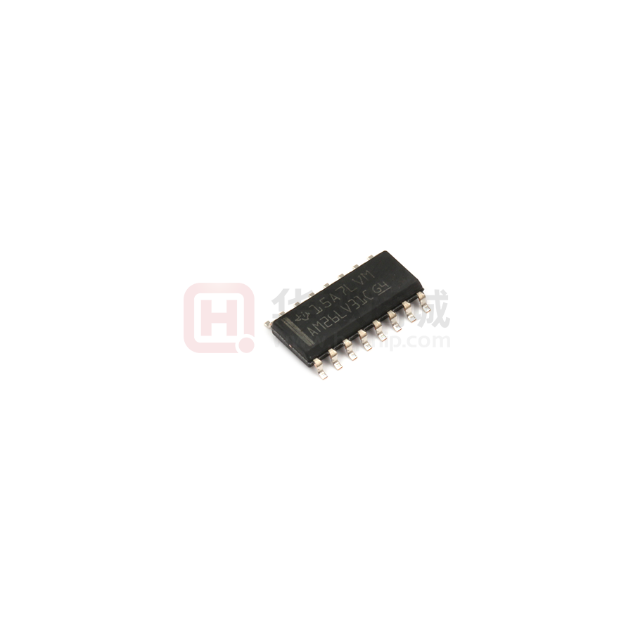
Package Options Include Plastic Small-Outline (D,
NS) Packages
•
The AM26LV31C is characterized for operation from
0°C to 70°C. The AM26LV31I is characterized for
operation from –45°C to 85°.C
Device Information(1)
PART NUMBER
2 Applications
•
•
The devices are optimized for balanced-bus
transmission at switching rates up to 32 MHz. The
outputs have very high current capability for driving
balanced lines such as twisted-pair transmission lines
and provide a high impedance in the power-off
condition. The enable function is common to all four
drivers and offers the choice of active-high or activelow enable inputs. The AM26LV31C and AM26LV31I
are designed using Texas Instruments proprietary
LinIMPACT-C60™ technology, facilitating ultra-low
power consumption without sacrificing speed. These
devices offer optimum performance when used with
the AM26LV32 quadruple line receivers.
AM26LV31C
Motor Control: Brushless DC and Brushed DC
Field Transmitters: Temperature Sensors and
Pressure Sensors
Temperature Sensors or Controllers Using
Modbus
AM26LV31I
PACKAGE
BODY SIZE (NOM)
SOIC (D) 16
9.90 mm x 3.91 mm
SOIC (D) 16
9.90 mm x 3.91 mm
SO (NS) 16
10.3 mm x 5.30 mm
(1) For all available packages, see the orderable addendum at
the end of the data sheet.
Logic Diagram (Positive Logic)
G
G
1A
2A
3A
4A
4
12
1
2
3
7
6
5
9
10
11
15
14
13
1Y
1Z
2Y
2Z
3Y
3Z
4Y
4Z
1
An IMPORTANT NOTICE at the end of this data sheet addresses availability, warranty, changes, use in safety-critical applications,
intellectual property matters and other important disclaimers. PRODUCTION DATA.
�AM26LV31
SLLS201H – MAY 1995 – REVISED APRIL 2018
www.ti.com
Table of Contents
1
2
3
4
5
6
7
8
Features ..................................................................
Applications ...........................................................
Description .............................................................
Revision History.....................................................
Pin Configuration and Functions .........................
Specifications.........................................................
1
1
1
2
3
4
6.1
6.2
6.3
6.4
6.5
6.6
6.7
4
4
4
4
5
5
6
Absolute Maximum Ratings ......................................
ESD Ratings..............................................................
Recommended Operating Conditions.......................
Thermal Information ..................................................
Electrical Characteristics..........................................
Switching Characteristics.........................................
Typical Characteristics ..............................................
Parameter Measurement Information .................. 7
Detailed Description ............................................ 10
8.1 Overview ................................................................. 10
8.2 Functional Block Diagram ....................................... 10
8.3 Feature Description................................................. 10
8.4 Device Functional Modes........................................ 11
9
Application and Implementation ........................ 12
9.1 Application Information............................................ 12
9.2 Typical Application ................................................. 12
10 Power Supply Recommendations ..................... 13
11 Layout................................................................... 14
11.1 Layout Guidelines ................................................. 14
11.2 Layout Example .................................................... 14
12 Device and Documentation Support ................. 15
12.1
12.2
12.3
12.4
12.5
12.6
Device Support ....................................................
Receiving Notification of Documentation Updates
Community Resources..........................................
Trademarks ...........................................................
Electrostatic Discharge Caution ............................
Glossary ................................................................
15
15
15
15
15
15
13 Mechanical, Packaging, and Orderable
Information ........................................................... 15
4 Revision History
NOTE: Page numbers for previous revisions may differ from page numbers in the current version.
Changes from Revision G (May 2005) to Revision H
Page
•
Added Device Information table, ESD Ratings table, Feature Description section, Device Functional Modes,
Application and Implementation section, Power Supply Recommendations section, Layout section, Device and
Documentation Support section, and Mechanical, Packaging, and Orderable Information section ..................................... 1
•
Changed the tPLH and tPHL MAX value From: 12 ns To: 20 ns in the Switching Characteristics ........................................... 5
•
Changed the tsk(p) and tsk(o) MAX value From: 1.5 ns To: 3 ns in the Switching Characteristics ........................................... 5
2
Submit Documentation Feedback
Copyright © 1995–2018, Texas Instruments Incorporated
Product Folder Links: AM26LV31
�AM26LV31
www.ti.com
SLLS201H – MAY 1995 – REVISED APRIL 2018
5 Pin Configuration and Functions
D or NS Package
SOIC 16 Pins
Top View
1A
1
16
VCC
1Y
2
15
4A
1Z
3
14
4Y
G
4
13
4Z
2Z
5
12
G
2Y
6
11
3Z
2A
7
10
3Y
GND
8
9
3A
Not to scale
Pin Functions
PIN
NO.
NAME
I/O
DESCRIPTION
1
1A
I
Driver 1 input
2
1Y
O
Driver 1 output
3
1Z
O
Driver 1 inverted output
4
G
I
Active high enable
5
2Z
O
Driver 2 inverted output
6
2Y
O
Driver 2 output
7
2A
I
Driver 2 input
8
GND
9
3A
I
Driver 3 input
10
3Y
O
Driver 3 output
11
3Z
O
Driver 3 inverted output
12
G
I
Active low enable
13
4Z
O
Driver 4 inverted output
14
4Y
O
Driver 4 output
15
4A
I
Driver 4 input
16
VCC
—
—
Ground pin
Power pin
Submit Documentation Feedback
Copyright © 1995–2018, Texas Instruments Incorporated
Product Folder Links: AM26LV31
3
�AM26LV31
SLLS201H – MAY 1995 – REVISED APRIL 2018
www.ti.com
6 Specifications
6.1 Absolute Maximum Ratings
over operating free-air temperature range (unless otherwise noted) (1)
MIN
MAX
UNIT
Supply voltage range, VCC (2)
–0.3
6
V
Input voltage range, VI
–0.3
6
V
Output voltage range, VO
–0.3
6
V
Storage temperature, Tstg
–65
150
°C
(1)
(2)
Stresses beyond those listed under Absolute Maximum Ratings may cause permanent damage to the device. These are stress ratings
only, which do not imply functional operation of the device at these or any other conditions beyond those indicated under Recommended
Operating Conditions. Exposure to absolute-maximum-rated conditions for extended periods may affect device reliability.
All voltage values are with respect to GND.
6.2 ESD Ratings
VALUE
Human-body model (HBM), per ANSI/ESDA/JEDEC JS-001
V(ESD)
(1)
(2)
Electrostatic discharge
(1)
UNIT
±3000
Charged-device model (CDM), per JEDEC specification JESD22C101 (2)
V
±250
JEDEC document JEP155 states that 500-V HBM allows safe manufacturing with a standard ESD control process. .
JEDEC document JEP157 states that 250-V CDM allows safe manufacturing with a standard ESD control process.
6.3 Recommended Operating Conditions
MIN
NOM
MAX
VCC
Supply voltage
3
3.3
3.6
VIH
High-level input voltage
2
VIL
Low-level input voltage
0.8
V
IOH
High-level output current
–30
mA
IOL
Low-level output current
30
mA
0
70
°C
–45
85
°C
TA
Operating free-air temperature
AM26LV31C
AM26LV31I
UNIT
V
V
6.4 Thermal Information
THERMAL METRIC (1)
D (SOIC)
NS (SO)
16 PINS
16 PINS
UNIT
RθJA
Junction-to-ambient thermal resistance
81.9
76.9
°C/W
RθJC(top)
Junction-to-case (top) thermal resistance
40.3
33.1
°C/W
RθJB
Junction-to-board thermal resistance
40.1
37.1
°C/W
ψJT
Junction-to-top characterization parameter
7.9
4.3
°C/W
ψJB
Junction-to-board characterization parameter
39.8
37.3
°C/W
RθJC(bot)
Junction-to-case (bottom) thermal resistance
n/a
n/a
°C/W
(1)
4
For more information about traditional and new thermal metrics, see the Semiconductor and IC Package Thermal Metrics application
report.
Submit Documentation Feedback
Copyright © 1995–2018, Texas Instruments Incorporated
Product Folder Links: AM26LV31
�AM26LV31
www.ti.com
6.5
SLLS201H – MAY 1995 – REVISED APRIL 2018
Electrical Characteristics
over recommended operating supply-voltage and free-air temperature ranges (unless otherwise noted)
PARAMETER
TEST CONDITIONS
VIK
Input clamp voltage
II = 18 mA
VOH
High-level output voltage
VIH = 2 V,
IOH = –12 mA
VOL
Low-level output voltage
VIL = 0.8 V,
IOH = 12 mA
|VOD|
Differential output voltage (2)
VOC
Common-mode output voltage
Δ|VOC|
Change in magnitude of
common-mode output voltage (2)
IO
Output current with power off
VO = –0.25 V or 6 V,
IOZ
Off-state (high-impedance state)
output current
IH
MIN
TYP (1)
1.85
2.3
0.8
0.95
1.5
1.3
1.55
MAX
UNIT
–1.5
V
V
1.05
V
V
1.8
V
±0.2
V
VCC = 0
±100
μA
VO = –0.25 V or 6 V,
G = 0.8 V or G = 2 V
±100
μA
High-level input current
VCC = 0 or 3 V,
VI = 5.5 V
10
μA
IL
Low-level input current
VCC = 3.6 V,
VI = 0
–10
μA
IOS
Short-circuit output current
VCC = 3.6 V,
VO = 0
–200
mA
ICC
Supply current (all drivers)
VI = VCC or GND,
No load
100
μA
Cpd
Power-dissipation capacitance
(all drivers) (3)
No load
(1)
(2)
(3)
RL = 100 Ω
160
pF
All typical values are at VCC = 3.3 V, TA = 25°C.
Δ|VOD| and Δ|VOC| are the changes in magnitude of VOD and VOC, respectively, that occur when the input is changed from a high level to
a low level.
Cpd determines the no-load dynamic current consumption. IS = Cpd × VCC × f + ICC
6.6
Switching Characteristics
VCC = 3.3 V, TA = 25°C
PARAMETER
TEST CONDITIONS
tPLH
Propagation delay time, low- to high-level output
tPHL
Propagation delay time, high- to low-level output
tt
Transition time (tr or tf)
See Figure 3
MIN
TYP (1)
MAX
4
8
20
ns
4
8
20
ns
3
(2)
ns
SR
Slew rate, single-ended output voltage
See Note
0.3
1
V/ns
tPZH
Output-enable time to high level
See Figure 4
10
20
ns
tPZL
Output-enable time to low level
See Figure 5
10
20
ns
tPHZ
Output-disable time from high level
See Figure 4
10
20
ns
tPLZ
Output-disable time from low level
See Figure 5
10
20
ns
tsk(p)
Pulse skew
f = 32 MHz,
0.5
3
ns
tsk(o)
Skew limit
f = 32 MHz
3
ns
3
ns
tsk(lim)
(1)
(2)
(3)
(4)
Skew limit (device to device)
f = 32 MHz,
and Figure 3
UNIT
See Note
See Note
(3)
(4)
All typical values are at VCC = 3.3 V, TA = 25°C.
Slew rate is defined by Equation 1
Pulse skew is defined as the |tPLH - tPHL| of each channel of the same device.
Skew limit (device to device) is the maximum difference in propagation delay times between any two channels of any two devices.
Submit Documentation Feedback
Copyright © 1995–2018, Texas Instruments Incorporated
Product Folder Links: AM26LV31
5
�AM26LV31
SLLS201H – MAY 1995 – REVISED APRIL 2018
SR =
90% (VOH
www.ti.com
- VOL) - 10% (VOH - VOL)
tr
, the differential slew rate of VCC is 2 x SR.
(1)
6.7 Typical Characteristics
30
-45qC
25qC
85qC
Current (mA)
25
20
15
10
5
0
0
5
10
15
20
Frequency (MHz)
25
30
35
D001
Figure 1. Current vs Frequency
6
Submit Documentation Feedback
Copyright © 1995–2018, Texas Instruments Incorporated
Product Folder Links: AM26LV31
�AM26LV31
www.ti.com
SLLS201H – MAY 1995 – REVISED APRIL 2018
7 Parameter Measurement Information
RL/2
Y
Z
A
VOD2
G
RL/2
VOC
G
Figure 2. Differential and Common-Mode Output Voltages
Y
A
Generator
(see Note B)
VCC
Z
CL = 15 pF
(see Note A)
RL = 100 :
VO
VOD
50 :
VO
G
G
TEST CIRCUIT
VCC
Input
50%
50%
A
0V
tPHL
tPLH
Z
Output, VO
Y
PROPAGATION DELAY TIMES
90%
10%
Y
VOH
90%
10%
tr
tf
tf
tr
VOL
Output, VO
Z
90%
90%
10%
10%
VOH
VOL
RISE AND FALL TIMES
A.
CL includes probe and jig capacitance.
B.
The input pulse is supplied by a generator having the following characteristics: PRR = 32 MHz, ZO = 50 Ω, 50%v duty
cycle, tr and tf ≤ 2 ns.
Figure 3. Test Circuit and Voltage Waveforms, tPHL and tPLH
Submit Documentation Feedback
Copyright © 1995–2018, Texas Instruments Incorporated
Product Folder Links: AM26LV31
7
�AM26LV31
SLLS201H – MAY 1995 – REVISED APRIL 2018
www.ti.com
Parameter Measurement Information (continued)
S1
Y
A
VCC
Z
Output
CL = 15 pF
(see Note A)
RL = 110 :
G
Generator
(see Note B)
G
50 :
VCC
(see Note C)
TEST CIRCUIT
VCC
50%
Input
50%
0V
tPHZ
tPZH
0.3 V
VOH
Output
50%
Voff C 0
VOLTAGE WAVEFORMS
A.
CL includes probe and jig capacitance.
B.
The input pulse is supplied by a generator having the following characteristics: PRR = 1 MHz, ZO = 50 Ω, 50%v duty
cycle, tr and tf (10% to 90%) ≤ 2 ns.
C.
To test the active-low enable G, ground G and apply an inverted waveform to G.
Figure 4. Test Circuit and Voltage Waveforms, tPZH and tPHZ
8
Submit Documentation Feedback
Copyright © 1995–2018, Texas Instruments Incorporated
Product Folder Links: AM26LV31
�AM26LV31
www.ti.com
SLLS201H – MAY 1995 – REVISED APRIL 2018
Parameter Measurement Information (continued)
VCC
Y
A
VCC
RL = 110 :
S1
Z
Output
CL = 15 pF
(see Note A)
G
Generator
(see Note B)
50 :
G
VCC
(see Note C)
TEST CIRCUIT
VCC
Input
50%
50%
0V
tPLZ
tPZL
Voff C VCC
Output
50%
VOL
VOLTAGE WAVEFORMS
0.3 V
A.
CL includes probe and jig capacitance.
B.
The input pulse is supplied by a generator having the following characteristics: PRR = 1 MHz, ZO = 50 Ω, 50%v duty
cycle, tr and tf (10% to 90%) ≤ 2 ns.
C.
To test the active-low enable G, ground G and apply an inverted waveform to G.
Figure 5. Test Circuit and Voltage Waveforms, tPZL and tPLZ
Submit Documentation Feedback
Copyright © 1995–2018, Texas Instruments Incorporated
Product Folder Links: AM26LV31
9
�AM26LV31
SLLS201H – MAY 1995 – REVISED APRIL 2018
www.ti.com
8 Detailed Description
8.1 Overview
The AM26LV31C and AM26LV31I are BiCMOS quadruple differential line drivers with 3-state outputs. The
devices are designed to be similar to TIA/EIA-422-B and ITU Recommendation V.11 drivers with a single 3.3-V
power supply. The drivers also integrate active-high and active-low enables for precise device control.
8.2 Functional Block Diagram
G
G
1A
2A
3A
4A
4
12
2
1
3
6
7
5
9
10
11
15
14
13
1Y
1Z
2Y
2Z
3Y
3Z
4Y
4Z
8.3 Feature Description
8.3.1 Active high and active low
The devices can be configured using the G and G logic inputs to select transmitter output. A logic high on the G
pin or a logic low on the G pin enables the device to operate. These pins are simply a way to configure the logic
to match that of the receiving or transmitting controller or microprocessor.
8.3.2 Operates from a 3.3-V Supply with up to 5-V Logic
While the transmitters operate from a single 3.3-V rail, the logic can operate off the same rail or another 5-V rail,
making designs much more flexible to communicate to controllers.
8.3.3 High Speed Transmission
The AM26LV31C and AM26LV31I are optimized for balanced-bus transmission at switching rates up to 32 MHz.
The devices are designed using Texas Instruments proprietary LinIMPACT-C60™ technology, facilitating ultralow power consumption without sacrificing speed.
10
Submit Documentation Feedback
Copyright © 1995–2018, Texas Instruments Incorporated
Product Folder Links: AM26LV31
�AM26LV31
www.ti.com
SLLS201H – MAY 1995 – REVISED APRIL 2018
8.4 Device Functional Modes
Table 1. Function Table (1)
(1)
ENABLES
OUTPUTS
INPUT
A
G
G
Y
H
H
X
H
L
L
H
X
L
H
H
X
L
H
L
L
X
L
L
H
X
L
H
Z
Z
Z
H = high level, L = low level, X = irrelevant, Z = high impedance (off)
EQUIVALENT OF EACH INPUT (A, G, OR G)
TYPICAL OF ALL OUTPUTS (Y AND Z)
VCC
VCC
100 :
40 k:
6:
Input
Output
GND
GND
ll resistor values are nominal.
Figure 6. Schematic (Each Driver)
Submit Documentation Feedback
Copyright © 1995–2018, Texas Instruments Incorporated
Product Folder Links: AM26LV31
11
�AM26LV31
SLLS201H – MAY 1995 – REVISED APRIL 2018
www.ti.com
9 Application and Implementation
NOTE
Information in the following applications sections is not part of the TI component
specification, and TI does not warrant its accuracy or completeness. TI’s customers are
responsible for determining suitability of components for their purposes. Customers should
validate and test their design implementation to confirm system functionality.
9.1 Application Information
When designing a system that uses drivers, receivers, and transceivers, proper cable termination is essential for
highly reliable applications with reduced reflections in the transmission line. If termination is used, it can be
placed at the end of the cable near the last receiver. Factors to consider when determining the type of
termination usually are performance requirements of the application and the ever-present factor, cost. The
different types of termination techniques discussed are unterminated lines, parallel termination, AC termination,
and multipoint termination. For laboratory experiments, 100 feet of 100-Ω, 24-AWG, twisted-pair cable (Bertek)
was used. A single driver and receiver, TI AM26LV31C and AM26LV32C, respectively, were tested at room
temperature with a 3.3-V supply voltage. The first plot shows output waveforms from the driver at the start of the
cable (A/B); the second plot shows input waveforms to the receiver at the far end of the cable (Y).
9.2 Typical Application
VCC
VCC
0.1 PF
Input 1 Signal
1A
1Y
Output 1
Differential Pair
1Z
G
2Z
Output 2
Differential Pair
Input 2 Signal
2Y
2A
16
1
15
2
14
3
13
4
12
5
11
6
10
7
9
4A
Input 4 Signal
4Y
4Z
G
Output 4
Differential Pair
Active Low Enable Signal
3Z
3Y
3A
Output 3
Differential Pair
Input 3 Signal
8
GND
Figure 7. Differential Terminated Configuration With All Channels and Active Low Enable Used
12
Submit Documentation Feedback
Copyright © 1995–2018, Texas Instruments Incorporated
Product Folder Links: AM26LV31
�AM26LV31
www.ti.com
SLLS201H – MAY 1995 – REVISED APRIL 2018
Typical Application (continued)
9.2.1 Design Requirements
Resistor and capacitor (if used) termination values are shown for each laboratory experiment, but vary from
system to system. For example, the termination resistor, RT, must be within 20% of the characteristic
impedance, Zo, of the cable and can vary from about 80 Ω to 120 Ω.
This example requires the following:
• 3.3-V power source
• RS-485 bus operating at 32 MHz or less
• Connector that ensures the correct polarity for port pins
9.2.2 Detailed Design Procedure
Ensure values in Absolute Maximum Ratings are not exceeded. Supply voltage, VIH, and VIL must comply with
Recommended Operating Conditions.
Place the device close to bus connector to keep traces (stub) short to prevent adding reflections to the bus line.
If desired, add external fail-safe biasing to ensure 200 mV on the A-B port, if the drive is in high impedance state
(see Failsafe in RS-485 data buses).
9.2.3 Application Curves
5
4
Voltage (V)
3
2
1
0
±1
±2
Y
A/B
±3
0
0.1
0.2
0.3
Time ( s)
0.4
0.5
C001
Figure 8. Differential 120-Ω Terminated Output Waveforms (Cat 5E Cable)
10 Power Supply Recommendations
Place a 0.1-μF bypass capacitors close to the power-supply pins to reduce errors coupling in from noisy or high
impedance power supplies.
Submit Documentation Feedback
Copyright © 1995–2018, Texas Instruments Incorporated
Product Folder Links: AM26LV31
13
�AM26LV31
SLLS201H – MAY 1995 – REVISED APRIL 2018
www.ti.com
11 Layout
11.1 Layout Guidelines
For best operational performance of the device, use good PCB layout practices, including:
• Noise can propagate into analog circuitry through the power pins of the circuit as a whole, as well as the
operational amplifier. Bypass capacitors are used to reduce the coupled noise by providing low impedance
power sources local to the analog circuitry. Connect low-ESR, 0.1-μF ceramic bypass capacitors between
supply pin and ground, placed as close to the device as possible.
• Separate grounding for analog and digital portions of circuitry is one of the simplest and most effective
methods of noise suppression. One or more layers on multilayer PCBs are usually devoted to ground planes.
A ground plane helps distribute heat and reduces EMI noise pickup. Make sure to physically separate digital
and analog grounds, paying attention to the flow of the ground current.
• To reduce parasitic coupling, run the input traces as far away from the supply or output traces as possible. If
it is not possible to keep them separate, it is much better to cross the sensitive trace perpendicular as
opposed to in parallel with the noisy trace.
• Keep the length of input traces as short as possible. Always remember that the input traces are the most
sensitive part of the circuit.
• Consider a driven, low-impedance guard ring around the critical traces. A guard ring can significantly reduce
leakage currents from nearby traces that are at different potentials.
11.2 Layout Example
Differential
Output 1
0.1 PF
Input 1
VCC
1
1A
VCC 16
2
1Y
4A 15
3
1Z
4Y 14
4
G
4Z 13
AM26LV31
Differential
Output 2
Input 2
5
2Z
G 12
6
2Y
3Z 11
7
2A
3Y 10
8
GND
3A
Active Low
Enable
9
Figure 9. Trace Layout on PCB and Recommendations
14
Submit Documentation Feedback
Copyright © 1995–2018, Texas Instruments Incorporated
Product Folder Links: AM26LV31
�AM26LV31
www.ti.com
SLLS201H – MAY 1995 – REVISED APRIL 2018
12 Device and Documentation Support
12.1 Device Support
12.1.1 Development Support
12.2 Receiving Notification of Documentation Updates
To receive notification of documentation updates, navigate to the device product folder on ti.com. In the upper
right corner, click on Alert me to register and receive a weekly digest of any product information that has
changed. For change details, review the revision history included in any revised document.
12.3 Community Resources
The following links connect to TI community resources. Linked contents are provided "AS IS" by the respective
contributors. They do not constitute TI specifications and do not necessarily reflect TI's views; see TI's Terms of
Use.
TI E2E™ Online Community TI's Engineer-to-Engineer (E2E) Community. Created to foster collaboration
among engineers. At e2e.ti.com, you can ask questions, share knowledge, explore ideas and help
solve problems with fellow engineers.
Design Support TI's Design Support Quickly find helpful E2E forums along with design support tools and
contact information for technical support.
12.4 Trademarks
LinIMPACT-C60, E2E are trademarks of Texas Instruments.
All other trademarks are the property of their respective owners.
12.5 Electrostatic Discharge Caution
This integrated circuit can be damaged by ESD. Texas Instruments recommends that all integrated circuits be handled with
appropriate precautions. Failure to observe proper handling and installation procedures can cause damage.
ESD damage can range from subtle performance degradation to complete device failure. Precision integrated circuits may be more
susceptible to damage because very small parametric changes could cause the device not to meet its published specifications.
12.6 Glossary
SLYZ022 — TI Glossary.
This glossary lists and explains terms, acronyms, and definitions.
13 Mechanical, Packaging, and Orderable Information
The following pages include mechanical, packaging, and orderable information. This information is the most
current data available for the designated devices. This data is subject to change without notice and revision of
this document. For browser-based versions of this data sheet, refer to the left-hand navigation.
Submit Documentation Feedback
Copyright © 1995–2018, Texas Instruments Incorporated
Product Folder Links: AM26LV31
15
�PACKAGE OPTION ADDENDUM
www.ti.com
13-Aug-2021
PACKAGING INFORMATION
Orderable Device
Status
(1)
Package Type Package Pins Package
Drawing
Qty
Eco Plan
(2)
Lead finish/
Ball material
MSL Peak Temp
Op Temp (°C)
Device Marking
(3)
(4/5)
(6)
AM26LV31CD
ACTIVE
SOIC
D
16
40
RoHS & Green
NIPDAU
Level-1-260C-UNLIM
0 to 70
AM26LV31C
AM26LV31CDE4
ACTIVE
SOIC
D
16
40
RoHS & Green
NIPDAU
Level-1-260C-UNLIM
0 to 70
AM26LV31C
AM26LV31CDG4
ACTIVE
SOIC
D
16
40
RoHS & Green
NIPDAU
Level-1-260C-UNLIM
0 to 70
AM26LV31C
AM26LV31CDR
ACTIVE
SOIC
D
16
2500
RoHS & Green
NIPDAU | SN
Level-1-260C-UNLIM
0 to 70
AM26LV31C
AM26LV31CDRE4
ACTIVE
SOIC
D
16
2500
RoHS & Green
NIPDAU
Level-1-260C-UNLIM
0 to 70
AM26LV31C
AM26LV31CDRG4
ACTIVE
SOIC
D
16
2500
RoHS & Green
NIPDAU
Level-1-260C-UNLIM
0 to 70
AM26LV31C
AM26LV31CNSR
ACTIVE
SO
NS
16
2000
RoHS & Green
NIPDAU
Level-1-260C-UNLIM
0 to 70
26LV31
AM26LV31ID
ACTIVE
SOIC
D
16
40
RoHS & Green
NIPDAU
Level-1-260C-UNLIM
-45 to 85
AM26LV31I
AM26LV31IDR
ACTIVE
SOIC
D
16
2500
RoHS & Green
NIPDAU
Level-1-260C-UNLIM
-45 to 85
AM26LV31I
AM26LV31INSR
ACTIVE
SO
NS
16
2000
RoHS & Green
NIPDAU
Level-1-260C-UNLIM
-45 to 85
26LV31I
(1)
The marketing status values are defined as follows:
ACTIVE: Product device recommended for new designs.
LIFEBUY: TI has announced that the device will be discontinued, and a lifetime-buy period is in effect.
NRND: Not recommended for new designs. Device is in production to support existing customers, but TI does not recommend using this part in a new design.
PREVIEW: Device has been announced but is not in production. Samples may or may not be available.
OBSOLETE: TI has discontinued the production of the device.
(2)
RoHS: TI defines "RoHS" to mean semiconductor products that are compliant with the current EU RoHS requirements for all 10 RoHS substances, including the requirement that RoHS substance
do not exceed 0.1% by weight in homogeneous materials. Where designed to be soldered at high temperatures, "RoHS" products are suitable for use in specified lead-free processes. TI may
reference these types of products as "Pb-Free".
RoHS Exempt: TI defines "RoHS Exempt" to mean products that contain lead but are compliant with EU RoHS pursuant to a specific EU RoHS exemption.
Green: TI defines "Green" to mean the content of Chlorine (Cl) and Bromine (Br) based flame retardants meet JS709B low halogen requirements of