Product
Folder
Order
Now
Support &
Community
Tools &
Software
Technical
Documents
AM26LV32, AM26LV32I
SLLS202G – MAY 1995 – REVISED OCTOBER 2017
AM26LV32 Low-Voltage, High-Speed Quadruple Differential Line Receiver
1 Features
3 Description
•
•
•
•
The AM26LV32 device is a BiCMOS, quadruple
differential line receiver with 3-state outputs, which is
designed to be similar to the TIA/EIA-422-B and ITU
Recommendation V.11 receivers with reduced
common-mode voltage range due to reduced supply
voltage.
1
•
•
•
•
•
Switching Rates Up to 32 MHz
Operates From Single 3.3-V Supply
Ultra-Low Power Dissipation: 27 mW Typical
Open-Circuit, Short-Circuit, and Terminated
Fail-Safe
−0.3-V to 5.5-V Common-Mode Range With
±200-mV Sensitivity
Accepts 5-V Logic Inputs With 3.3-V VCC
Input Hysteresis: 50 mV Typical
235 mW With Four Receivers at 32 MHz
Pin-to-Pin Compatible With AM26C32 and
AM26LS32
The device is optimized for balanced bus
transmission at switching rates up to 32 MHz. The
enable function is common to all four receivers and
offers a choice of active-high or active-low inputs.
The 3-state outputs permit connection directly to a
bus-organized system. Each device features high
input impedance, input hysteresis for increased noise
immunity, and input sensitivity of ±200 mV over a
common-mode input voltage range from −0.3 V to
5.5 V. When the inputs are open-circuit, the outputs
are in the high logic state.
2 Applications
•
•
•
•
•
High-Reliability Automotive Applications
Factory Automation
ATM and Cash Counters
Smart Grid
AC and Servo Motor Drives
The AM26LV32C is characterized for operation from
0°C to 70°C. The AM26LV32I is characterized for
operation from −45°C to 85°C.
Device Information(1)
PART NUMBER
PACKAGE
BODY SIZE (NOM)
AM26LV32D
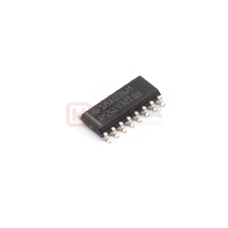
SOIC (16)
9.90 mm × 3.90 mm
AM26LV32NS
SO (16)
10.20 mm × 5.30 mm
(1) For all available packages, see the orderable addendum at
the end of the data sheet.
Logic Diagram (Positive Logic)
G
G
1A
4
12
2
3
1B
2A
6
5
2B
3A
4A
10
3Y
9
14
13
4B
2Y
7
11
3B
1Y
1
4Y
15
1
An IMPORTANT NOTICE at the end of this data sheet addresses availability, warranty, changes, use in safety-critical applications,
intellectual property matters and other important disclaimers. PRODUCTION DATA.
�AM26LV32, AM26LV32I
SLLS202G – MAY 1995 – REVISED OCTOBER 2017
www.ti.com
Table of Contents
1
2
3
4
5
6
7
8
Features ..................................................................
Applications ...........................................................
Description .............................................................
Revision History.....................................................
Pin Configuration and Functions .........................
Specifications.........................................................
1
1
1
2
3
4
6.1
6.2
6.3
6.4
6.5
6.6
6.7
4
4
4
4
5
5
6
Absolute Maximum Ratings ......................................
ESD Ratings..............................................................
Recommended Operating Conditions.......................
Thermal Information ..................................................
Electrical Characteristics...........................................
Switching Characteristics ..........................................
Typical Characteristics ..............................................
Parameter Measurement Information .................. 7
Detailed Description .............................................. 9
8.1 Overview ................................................................... 9
8.2 Functional Block Diagram ......................................... 9
8.3 Feature Description................................................... 9
8.4 Device Functional Modes........................................ 10
9
Application and Implementation ........................ 17
9.1 Application Information............................................ 17
9.2 Typical Application .................................................. 17
10 Power Supply Recommendations ..................... 19
11 Layout................................................................... 19
11.1 Layout Guidelines ................................................. 19
11.2 Layout Example .................................................... 19
12 Device and Documentation Support ................. 20
12.1
12.2
12.3
12.4
12.5
Receiving Notification of Documentation Updates
Community Resources..........................................
Trademarks ...........................................................
Electrostatic Discharge Caution ............................
Glossary ................................................................
20
20
20
20
20
13 Mechanical, Packaging, and Orderable
Information ........................................................... 20
4 Revision History
NOTE: Page numbers for previous revisions may differ from page numbers in the current version.
Changes from Revision F (November 2016) to Revision G
Page
•
Changed the MAX value of tsk(p) From: 6 ns To: 14 ns in the Switching Characteristics table .............................................. 5
•
Changed the MAX value of tsk(o) From: 6 ns To: 14 ns in the Switching Characteristics table .............................................. 5
Changes from Revision E (June 2005) to Revision F
Page
•
Added ESD Ratings table, Thermal Information table, Feature Description section, Device Functional Modes,
Application and Implementation section, Power Supply Recommendations section, Layout section, Device and
Documentation Support section, and Mechanical, Packaging, and Orderable Information section....................................... 1
•
Deleted MB570 from Features list .......................................................................................................................................... 1
•
Deleted Ordering Information table; see Mechanical, Packaging, and Orderable Information at the end of the data sheet. 1
•
Deleted Lead temperature (260°C maximum) from Absolute Maximum Ratings table.......................................................... 4
•
Changed Package thermal impedance, RθJA, values in Thermal Information table From: 73°C To: 72.9°C (D) and
From: 64°C To: 74°C (NS) ..................................................................................................................................................... 4
2
Submit Documentation Feedback
Copyright © 1995–2017, Texas Instruments Incorporated
Product Folder Links: AM26LV32
�AM26LV32, AM26LV32I
www.ti.com
SLLS202G – MAY 1995 – REVISED OCTOBER 2017
5 Pin Configuration and Functions
D and NS Package
16-Pin SOIC and SO
Top View
1B
1
16
VCC
1A
2
15
4B
1Y
3
14
4A
G
4
13
4Y
2Y
5
12
G
2A
6
11
3Y
2B
7
10
3A
GND
8
9
3B
Not to scale
Pin Functions
PIN
NAME
NO.
1A
2
1B
1Y
I/O
DESCRIPTION
I
RS422, RS485 differential input (noninverting)
1
I
RS422, RS485 differential input (inverting)
3
O
Logic level output
2A
6
I
RS422, RS485 differential input (noninverting)
2B
7
I
RS422, RS485 differential input (inverting)
2Y
5
O
Logic level output
3A
10
I
RS422, RS485 differential input (noninverting)
3B
9
I
RS422, RS485 differential input (inverting)
3Y
11
O
Logic level output
4A
14
I
RS422, RS485 differential input (noninverting)
4B
15
I
RS422, RS485 differential input (inverting)
4Y
13
O
Logic level output
G
12
I
Active-low select
G
4
I
Active-high select
GND
8
—
Ground
VCC
16
—
Power supply
Submit Documentation Feedback
Copyright © 1995–2017, Texas Instruments Incorporated
Product Folder Links: AM26LV32
3
�AM26LV32, AM26LV32I
SLLS202G – MAY 1995 – REVISED OCTOBER 2017
www.ti.com
6 Specifications
6.1 Absolute Maximum Ratings
Over operating free-air temperature range (unless otherwise noted) (1)
Supply voltage, VCC (2)
Input voltage, VI
MIN
MAX
UNIT
–0.3
6
V
–4
Differential input voltage, VID (3)
Enable input voltage
–0.3
Output voltage, VO
–0.3
Maximum output current, IO
Storage temperature, Tstg
(1)
(2)
(3)
–65
8
V
±12
V
6
V
6
V
±25
mA
150
°C
Stresses beyond those listed under Absolute Maximum Ratings may cause permanent damage to the device. These are stress ratings
only, which do not imply functional operation of the device at these or any other conditions beyond those indicated under Recommended
Operating Conditions. Exposure to absolute-maximum-rated conditions for extended periods may affect device reliability.
All voltage values are with respect to the GND terminal.
Differential input voltage is measured at the noninverting input with respect to the corresponding inverting input.
6.2 ESD Ratings
VALUE
V(ESD)
(1)
(2)
Electrostatic discharge
Human-body model (HBM), per ANSI/ESDA/JEDEC JS-001
(1)
UNIT
±500
Charged-device model (CDM), per JEDEC specification JESD22-C101 (2)
V
±500
JEDEC document JEP155 states that 500-V HBM allows safe manufacturing with a standard ESD control process.
JEDEC document JEP157 states that 250-V CDM allows safe manufacturing with a standard ESD control process.
6.3 Recommended Operating Conditions
over operating free-air temperature range (unless otherwise noted)
MIN
NOM
MAX
Supply voltage, VCC
3
3.3
3.6
High-level input voltage, VIH(EN)
2
V
V
Low-level input voltage, VIL(EN)
Common-mode input voltage, VIC
UNIT
–0.3
0.8
V
5.5
V
Differential input voltage, VID
±5.8
High-level output current, IOH
–5
mA
Low-level output current, IOL
5
mA
Operating free-air temperature, TA
AM26LV32C
AM26LV32I
0
70
–40
85
V
°C
6.4 Thermal Information
AM26LV32
THERMAL METRIC
(1) (2)
D (SOIC)
NS (SO)
16 PINS
16 PINS
UNIT
RθJA
Junction-to-ambient thermal resistance
72.9
74
°C/W
RθJC(top)
Junction-to-case (top) thermal resistance
32.4
31.1
°C/W
RθJB
Junction-to-board thermal resistance
30.4
34.8
°C/W
ψJT
Junction-to-top characterization parameter
5.4
5.1
°C/W
ψJB
Junction-to-board characterization parameter
30.1
34.5
°C/W
(1)
(2)
4
For more information about traditional and new thermal metrics, see the Semiconductor and IC Package Thermal Metrics application
report.
The package thermal impedance is calculated in accordance with JESD 51.
Submit Documentation Feedback
Copyright © 1995–2017, Texas Instruments Incorporated
Product Folder Links: AM26LV32
�AM26LV32, AM26LV32I
www.ti.com
SLLS202G – MAY 1995 – REVISED OCTOBER 2017
6.5 Electrical Characteristics
over operating free-air temperature range (unless otherwise noted)
PARAMETER
TEST CONDITIONS
VIT+
Differential input high-threshold voltage
VIT–
Differential input low-threshold voltage
VIK
Enable input clamp voltage
II = − 18 mA
VOH
High-level output voltage
VID = 200 mV, IOH = −5 mA
VOL
Low-level output voltage
VID = 200 mV, IOH = 5 mA
IOZ
High-impedance-state output current
VO = 0 to VCC
IIH(E)
High-level enable input current
VCC = 0 or 3 V, VI = 5.5 V
IIL(E)
Low-level enable input current
VCC = 3.6 V, VI = 0 V
rI
Input resistance
TYP (1)
MAX
UNIT
0.2
V
–0.2
II
Input current
ICC
Supply current
VI(E) = VCC or GND, no load, line
inputs open
Cpd
Power dissipation capacitance (2)
One channel
V
–0.8
2.4
–1.5
V
3.2
0.17
7
VI = 5.5 V or − 0.3 V, all other
inputs GND
(1)
(2)
MIN
V
0.5
V
±50
µA
10
µA
–10
µA
12
8
kΩ
±700
µA
17
mA
150
pF
All typical values are at VCC = 3.3 V and TA = 25°C.
Cpd determines the no-load dynamic current: IS = Cpd × VCC × f + ICC.
6.6 Switching Characteristics
over operating free-air temperature range (unless otherwise noted)
PARAMETER
TEST CONDITIONS
MIN
TYP
MAX
UNIT
tPLH
Propagation delay time,
low- to high-level output
See Figure 4
8
16
20
ns
tPHL
Propagation delay time,
high- to low-level output
See Figure 4
8
16
20
ns
tt
Transition time (tr or tf)
See Figure 4
5
tPZH
Output-enable time to high level
See Figure 5
17
40
ns
tPZL
Output-enable time to low level
See Figure 6
10
40
ns
tPHZ
Output-disable time from high level
See Figure 5
20
40
ns
tPLZ
Output-disable time from low level
See Figure 6
16
40
ns
tsk(p) (1)
Pulse skew
4
14
ns
(2)
Pulse skew
4
14
ns
Pulse skew (device to device)
6
9
ns
tsk(o)
tsk(pp) (3)
(1)
(2)
(3)
ns
tsk(p) is |tPLH − tPHL| of each channel of the same device.
tsk(o) is the maximum difference in propagation delay times between any two channels of the same device switching in the same
direction.
tsk(pp) is the maximum difference in propagation delay times between any two channels of any two devices switching in the same
direction.
Submit Documentation Feedback
Copyright © 1995–2017, Texas Instruments Incorporated
Product Folder Links: AM26LV32
5
�AM26LV32, AM26LV32I
SLLS202G – MAY 1995 – REVISED OCTOBER 2017
www.ti.com
6.7 Typical Characteristics
10
0.4
8
Output Leakage Current (mA)
0.6
Input Current (mA)
0.2
0.0
±0.2
±0.4
±0.6
±0.8
±1.0
A
±1.2
6
4
2
0
±2
±4
±6
Disabled
±8
B
Power Off
±10
±1.4
±4
±2
0
2
4
6
8
Common Mode Voltage (V)
±1
0
1
2
3
Output Voltage (V)
C002
Figure 1. RS422 Port Current vs Common-Mode Voltage
4
5
6
C003
Figure 2. Output Y Leakage Current vs Output Y Voltage
3.6
Output Drive Voltage (V)
3.2
2.8
2.4
2.0
VOL
1.6
VOH
1.2
0.8
0.4
0.0
0
5
10
15
20
Output Current (mA)
25
30
C004
Figure 3. Output Y Drive Voltage vs Output Y Current
6
Submit Documentation Feedback
Copyright © 1995–2017, Texas Instruments Incorporated
Product Folder Links: AM26LV32
�AM26LV32, AM26LV32I
www.ti.com
SLLS202G – MAY 1995 – REVISED OCTOBER 2017
7 Parameter Measurement Information
A
Generator
(see Note B)
Y
VO
B
50 Ω
CL = 15 pF
(see Note A)
50 Ω
A
2V
B
1V
Input
t PLH
Output
VCC
G
G
(see Note C)
t PHL
50%
10%
90%
tr
90%
VOH
50%
10% V
OL
tf
A.
CL includes probe and jig capacitance.
B.
The input pulse is supplied by a generator having the following characteristics: ZO = 50 Ω, PRR = 10 MHz, tr and tf
(10% to 90%) ≤ 2 ns, 50% duty cycle.
C.
To test the active-low enable G, ground G and apply an inverted waveform G.
Figure 4. tPLH and tPHL Test Circuit and Voltage Waveforms
VID = 1 V
A
Y
VO
B
CL = 15 pF
(see Note A)
RL = 2 kΩ
G
Generator
(see Note B)
50 Ω
G
VCC
(see Note C)
VCC
Input
50%
50%
0V
t PZH
Output
t PHZ
VOH
VOH − 0.3 V
Voff ≈ 0
A.
CL includes probe and jig capacitance.
B.
The input pulse is supplied by a generator having the following characteristics: ZO = 50 Ω, PRR = 10 MHz, tr and tf
(10% to 90%) ≤ 2 ns, 50% duty cycle.
C.
To test the active-low enable G, ground G and apply an inverted waveform G.
Figure 5. tPZH and tPHZ Test Circuit and Voltage Waveforms
Submit Documentation Feedback
Copyright © 1995–2017, Texas Instruments Incorporated
Product Folder Links: AM26LV32
7
�AM26LV32, AM26LV32I
SLLS202G – MAY 1995 – REVISED OCTOBER 2017
www.ti.com
Parameter Measurement Information (continued)
VCC
RL = 2 kΩ
A
VID = 1 V
Y
VO
B
CL = 15 pF
(see Note A)
G
Generator
(see Note B)
50 Ω
G
VCC
(see Note C)
VCC
Input
50%
50%
0V
t PZL
t PLZ
Voff ≈ VCC
Output
VOL + 0.3 V
VOL
A.
CL includes probe and jig capacitance.
B.
The input pulse is supplied by a generator having the following characteristics: ZO = 50 Ω, PRR = 10 MHz, tr and tf
(10% to 90%) ≤ 2 ns, 50% duty cycle.
C.
To test the active-low enable G, ground G and apply an inverted waveform G.
Figure 6. tPZL and tPLZ Test Circuit and Voltage Waveforms
8
Submit Documentation Feedback
Copyright © 1995–2017, Texas Instruments Incorporated
Product Folder Links: AM26LV32
�AM26LV32, AM26LV32I
www.ti.com
SLLS202G – MAY 1995 – REVISED OCTOBER 2017
8 Detailed Description
8.1 Overview
The AM26LV32 device is a quadruple differential line receiver that meets the necessary requirements for NSI
TIA/EIA-422-B, TIA/EIA-423-B, and ITU Recommendation V.10 and V.11. This device allows a low-power or lowvoltage MCU to interface with heavy machinery, subsystems, and other devices through long wires of up to
1000 m, giving any design a reliable and easy-to-use connection. As with any RS422 interface, the AM26LV32
works in a differential voltage range, which enables very good signal integrity.
8.2 Functional Block Diagram
G
G
1A
4
12
2
3
1B
2A
6
5
2B
3A
4A
10
3Y
9
14
13
4B
2Y
7
11
3B
1Y
1
4Y
15
Figure 7. Logic Diagram (Positive Logic)
8.3 Feature Description
The device can be configured using the G and G logic inputs to select receiver output. The high voltage or logic
1 on the G pin allows the device to operate on an active-high, and having a low voltage or logic 0 on the G
enables active-low operation. These are simple ways to configure the logic to match that of the receiving or
transmitting controller or microprocessor.
Equivalent of Each Input (A, B)
V CC
Equivalent of Each Enable Input (G, G)
Typical of All Outputs (Y)
VCC
VCC
7.2 kΩ
1.5 kΩ
100 Ω
A, B
15 kΩ
Enable
G, G
Y
GND
GND
1.5 kΩ
7.2 kΩ
GND
Copyright © 2016, Texas Instruments Incorporated
Figure 8. Schematics of Equivalent Inputs and Outputs
Submit Documentation Feedback
Copyright © 1995–2017, Texas Instruments Incorporated
Product Folder Links: AM26LV32
9
�AM26LV32, AM26LV32I
SLLS202G – MAY 1995 – REVISED OCTOBER 2017
www.ti.com
8.4 Device Functional Modes
The receivers implemented in these RS422 devices can be configured using the G and G logic pins to be
enabled or disabled. This allows the option to ignore or filter out transmissions as desired. Table 1 lists the
function of each receiver.
Table 1. Function Table (Each Receiver)
DIFFERENTIAL INPUT
OUTPUT (1)
G
G
H
X
H
X
L
H
H
X
?
X
L
?
H
X
L
X
L
L
Open, shorted, or
terminated (2)
H
X
H
X
L
H
X
L
H
Z
VID ≥ 0.2 V
–0.2 V < VID < 0.2 V
VID ≤ –0.2 V
(1)
(2)
ENABLES
H = high level, L = low level, X = irrelevant, Z = high impedance (off), ? = indeterminate
See Application and Implementation section
8.4.1 Fail-Safe Conditions
The AM26LV32 is a quadruple differential line receiver that is designed to function properly when appropriately
connected to active drivers. Applications do not always have ideal situations where all bits are being used, the
receiver inputs are never left floating, and fault conditions do not exist. In actuality, most applications have the
capability to either place the drivers in a high-impedance mode or power down the drivers altogether, and cables
may be purposely (or inadvertently) disconnected, both of which lead to floating receiver inputs. Furthermore,
even though measures are taken to avoid fault conditions like a short between the differential signals, this does
occur. The AM26LV32 device has an internal fail-safe circuitry which prevents the device from putting an
unknown voltage signal at the receiver outputs. In the following three cases, a high-state is produced at the
respective output:
1. Open fail-safe: Unused input pins are left open. Do not tie unused pins to ground or any other voltage.
Internal circuitry places the output in the high state.
2. 100-Ω terminated fail-safe: Disconnected cables, drivers in high-impedance state, or powered-down drivers
does not cause the AM26LV32 to malfunction. The outputs remain in a high state under these conditions.
When the drivers are either turned-off or placed into the high-impedance state, the receiver input may still be
able to pick up noise due to the cable acting as an antenna. To avoid having a large differential voltage being
generated, the use of twisted-pair cable induces the noise as a common-mode signal and is rejected.
3. Shorted fail-safe: Fault conditions that short the differential input pairs together does not cause incorrect data
at the outputs. A differential voltage (VID) of 0 V forces a high state at the outputs. Shorted fail-safe, however,
is not supported across the recommended common-mode input voltage (VIC) range. An unwanted state can
be induced to all outputs when an input is shorted and is biased with a voltage between −0.3 V and +5.5 V.
The shorted fail-safe circuitry functions properly when an input is shorted, but with no external commonmode voltage applied.
8.4.2 Fail-Safe Precautions
The internal fail-safe circuitry was designed such that the input common-mode (VIC) and differential (VID) voltages
must be observed. To ensure the outputs of unused or inactive receivers remain in a high state when the inputs
are open-circuited, shorted, or terminated, extra precaution must be taken on the active signal. In applications
where the drivers are placed in a high-impedance mode or are powered-down, TI recommends that for 1, 2, or 3
active receiver inputs, the low-level input voltage (VIL) must be greater than 0.4 V. As in all data transmission
applications, it is necessary to provide a return ground path between the two remote grounds (driver and receiver
ground references) to avoid ground differences. Table 2 and Figure 9 through Figure 11 are examples of active
input voltages with their respective waveforms and the effect each have on unused or inactive outputs. Note that
the active receivers behave as expected, regardless of the input levels.
10
Submit Documentation Feedback
Copyright © 1995–2017, Texas Instruments Incorporated
Product Folder Links: AM26LV32
�AM26LV32, AM26LV32I
www.ti.com
SLLS202G – MAY 1995 – REVISED OCTOBER 2017
Table 2. Active Receiver Inputs vs Outputs
1, 2, OR 3 ACTIVE INPUTS
VIL
VID
VIC
SEE FIGURE
1, 2, OR 3 ACTIVE
OUTPUTS
3, 2, OR 1 UNUSED
OR INACTIVE
OUTPUTS
High state
900 mV
200 mV
1V
Figure 9
Known state
–100 mV
200 mV
0V
Figure 10
Known state
?
600 mV
800 mV
1V
Figure 11
Known state
High state
0 mV
800 mV
400 mV
Figure 12
Known state
?
VIL = 900 mV
VIC = 1 V
Produces a High State at
Unused or Inactive Outputs
VID = 200 mV
0V
Figure 9. Waveform 1
VIC = 0 V
VL = -100 mV
An Unknown State is Produced
at Unused or Inactive Outputs
VID = 200 mV
Figure 10. Waveform 2
VID = 800 mV
VIL = 600 mV
Produces a High State at
Unused or Inactive Outputs
VIC = 1 V
0V
Figure 11. Waveform 3
VID = 800 mV
VIL = 0 V
An Unknown State is Produced
at Unused or Inactive Outputs
0V
VIC = 400 mV
Figure 12. Waveform 4
In most applications, having a common-mode input close to ground and a differential voltage larger than 2 V is
not customary. Because the common-mode input voltage is typically around 1.5 V, a 2-V VID would result in a VIL
of 0.5 V, thus satisfying the recommended VIL level of greater than 0.4 V.
Figure 13 plots seven different input threshold curves from a variety of production lots and shows how the failsafe circuitry behaves with the input common-mode voltage levels. These input threshold curves are
representative samples of production devices. The curves specifically illustrate a typical range of input threshold
variation. The AM26LV32 is specified with ±200 mV of input sensitivity to account for the variance in input
threshold. Each data point represents the input’s ability to produce a known state at the output for a given VIC
and VID. Applying a differential voltage at or above a certain point on a curve would produce a known state at the
Submit Documentation Feedback
Copyright © 1995–2017, Texas Instruments Incorporated
Product Folder Links: AM26LV32
11
�AM26LV32, AM26LV32I
SLLS202G – MAY 1995 – REVISED OCTOBER 2017
www.ti.com
output. Applying a differential voltage less than a certain point on a curve would activate the fail-safe circuit and
the output would be in a high state. For example, inspecting the top input threshold curve reveals that for a VIC
that is approximately 1.6 V, VID yields around 87 mV. Applying 90 mV of differential voltage to this particular
production lot generates a known receiver output voltage. Applying a VID of 80 mV activates the input fail-safe
circuitry and the receiver output is placed in the high state. Texas Instruments specifies the input threshold at
±200 mV, because normal process variations affect this parameter. Note that at common-mode input voltages
around 0.2 V, the input differential voltages are low compared to their respective data points. This phenomenon
points to the fact that the inputs are very sensitive to small differential voltages around 0.2 V VIC. TI recommends
that VIC levels be kept greater than 0.5 V to avoid this increased sensitivity at VIC ≈ 0.2 V. In most applications,
because VIC typically is 1.5 V, the fail-safe circuitry functions properly to provide a high state at the receiver
output.
Most
Applications
100
90
VID − Differential Voltage − mV
80
70
60
Not
Recommended
50
40
30
20
10
Increased Receiver Input Sensitivity
0
−1 −0.8 −0.6 −0.4 −0.2
0
0.2 0.4 0.6 0.8
1
1.2 1.4 1.6 1.8
2
2.2
2.4
VIC − Common-Mode Input Voltage − V
Figure 13. VIC vs VID Receiver Sensitivity Levels
Figure 14 represents a typical application where two receivers are not used. In this case, there is no need to
worry about the output voltages of the unused receivers because these are not connected in the system
architecture.
12
Submit Documentation Feedback
Copyright © 1995–2017, Texas Instruments Incorporated
Product Folder Links: AM26LV32
�AM26LV32, AM26LV32I
www.ti.com
SLLS202G – MAY 1995 – REVISED OCTOBER 2017
AM26LV32
Connector
RT
System
RT
Unused Circuit
Copyright © 2016, Texas Instruments Incorporated
Figure 14. Typical Application With Unused Receivers
Figure 15 shows a common application where one or more drivers are either disabled or powered down. To
ensure the inactive receiver outputs are in a high state, the active receiver inputs must have VIL > 0.4 V and
VIC > 0.5 V.
Driver
Connector
AM26LV32
Connector
RT
Enable
RT
Cable
System
RT
Disable or
Power Off
RT
Copyright © 2016, Texas Instruments Incorporated
Figure 15. Typical Application Where Two or More Drivers Are Disabled
Figure 16 is an alternative application design to replace the application in Figure 15. This design uses two
AM26LV32 devices instead of one. However, this design does not require the input levels be monitored to ensure
the outputs are in the correct state, only that they comply to the RS-232 standard.
Submit Documentation Feedback
Copyright © 1995–2017, Texas Instruments Incorporated
Product Folder Links: AM26LV32
13
�AM26LV32, AM26LV32I
SLLS202G – MAY 1995 – REVISED OCTOBER 2017
www.ti.com
Driver
Connector
AM26LV32
Connector
RT
Enable
RT
Cable
Unused Circuit
Disable or
Power Off
System
AM26LV32
RT
RT
Unused Circuit
Copyright © 2016, Texas Instruments Incorporated
Figure 16. Alternative Solution for Figure 15
Figure 17 and Figure 18 show typical applications where a disconnected cable occurs. Figure 17 illustrates a
typical application where a cable is disconnected. Similar to Figure 15, the active input levels must be monitored
to make sure the inactive receiver outputs are in a high state. An alternative solution is shown in Figure 18.
14
Submit Documentation Feedback
Copyright © 1995–2017, Texas Instruments Incorporated
Product Folder Links: AM26LV32
�AM26LV32, AM26LV32I
www.ti.com
SLLS202G – MAY 1995 – REVISED OCTOBER 2017
Driver
Connector
AM26LV32
Connector
Cable
RT
RT
System
Unplugged
Cable
RT
RT
Copyright © 2016, Texas Instruments Incorporated
Figure 17. Typical Application Where Two or More Drivers Are Disconnected
Figure 18 is an alternative solution so the receiver inputs do not have to be monitored. This solution also requires
the use of two AM26LV32 devices instead of one.
Submit Documentation Feedback
Copyright © 1995–2017, Texas Instruments Incorporated
Product Folder Links: AM26LV32
15
�AM26LV32, AM26LV32I
SLLS202G – MAY 1995 – REVISED OCTOBER 2017
www.ti.com
Driver
AM26LV32
Connector
Connector
RT
Cable
RT
Unused Circuit
System
AM26LV32
Unplugged
Cable
RT
RT
Unused Circuit
Copyright © 2016, Texas Instruments Incorporated
Figure 18. Alternative Solution to Figure 17
When designing a system using the AM26LV32, the device provides a robust solution where fail-safe and fault
conditions are of concern. The RS422-like inputs accept common-mode input levels from −0.3 V to 5.5 V with a
specified sensitivity of ±200mV. As previously shown, take care with active input levels because this can affect
the outputs of unused or inactive bits. However, most applications meet or exceed the requirements to allow the
device to perform properly.
16
Submit Documentation Feedback
Copyright © 1995–2017, Texas Instruments Incorporated
Product Folder Links: AM26LV32
�AM26LV32, AM26LV32I
www.ti.com
SLLS202G – MAY 1995 – REVISED OCTOBER 2017
9 Application and Implementation
NOTE
Information in the following applications sections is not part of the TI component
specification, and TI does not warrant its accuracy or completeness. TI’s customers are
responsible for determining suitability of components for their purposes. Customers should
validate and test their design implementation to confirm system functionality.
9.1 Application Information
When designing a system that uses drivers, receivers, and transceivers that comply with RS422 or RS485,
proper cable termination is essential for highly reliable applications with reduced reflections in the transmission
line. Because RS422 allows only one driver on the bus, if termination is used, it is placed only at the end of the
cable near the last receiver. In general, RS485 requires termination at both ends of the cable. Factors to
consider when determining the type of termination usually are performance requirements of the application and
the ever-present factor, cost. The different types of termination techniques include unterminated lines, parallel
termination, ac termination, and multipoint termination.
9.2 Typical Application
AM26LV31E
(One Driver)
AM26LV32E
(One Reciever)
RT
DIN
ROUT
D
D
Copyright © 2016, Texas Instruments Incorporated
Figure 19. Differential Terminated Configuration
9.2.1 Design Requirements
Resistor and capacitor (if used) termination values vary from system to system. The termination resistor, RT,
must be within 20% of the characteristic impedance, ROUT, of the cable and can vary from about 80 Ω to 120 Ω.
9.2.2 Detailed Design Procedure
Figure 19 shows a configuration with RT as termination. Although reflections are present at the receiver inputs at
a data signaling rate of 200 kbps with no termination, the RS422-compliant receiver reads only the input
differential voltage and produces a clean signal at the output.
Submit Documentation Feedback
Copyright © 1995–2017, Texas Instruments Incorporated
Product Folder Links: AM26LV32
17
�AM26LV32, AM26LV32I
SLLS202G – MAY 1995 – REVISED OCTOBER 2017
www.ti.com
Typical Application (continued)
9.2.3 Application Curve
2.0
A
Input Open Circuit Voltage (V)
1.8
B
1.6
1.4
1.2
1.0
0.8
0.6
0.4
0.2
0.0
0.8
1.2
1.6
2.0
2.4
2.8
VCC (V)
3.2
3.6
C001
Figure 20. RS422 Port Open-Circuit Voltage vs VCC
18
Submit Documentation Feedback
Copyright © 1995–2017, Texas Instruments Incorporated
Product Folder Links: AM26LV32
�AM26LV32, AM26LV32I
www.ti.com
SLLS202G – MAY 1995 – REVISED OCTOBER 2017
10 Power Supply Recommendations
Place 0.1-µF bypass capacitors close to the power-supply pins to reduce errors coupling in from noisy or highimpedance power supplies.
11 Layout
11.1 Layout Guidelines
For best operational performance of the device, use good PCB layout practices including:
• Noise can propagate into analog circuitry through the power pins of the circuit as a whole, as well as the
operational amplifier. Bypass capacitors are used to reduce the coupled noise by providing low impedance
power sources local to the analog circuitry.
• Connect low-ESR, 0.1-µF ceramic bypass capacitors between each supply pin and ground, placed as close
to the device as possible. A single bypass capacitor from V+ to ground is applicable for single-supply
applications.
• Separate grounding for analog and digital portions of circuitry is one of the simplest and most-effective
methods of noise suppression. One or more layers on multilayer PCBs are usually devoted to ground planes.
A ground plane helps distribute heat and reduces EMI noise pickup. Make sure to physically separate digital
and analog grounds, and pay attention to the flow of the ground current.
• To reduce parasitic coupling, run the input traces as far away from the supply or output traces as possible. If
it is not possible to keep them separate, it is much better to cross the sensitive trace perpendicular as
opposed to in parallel with the noisy trace.
• Place the external components as close to the device as possible. Keeping RF and RG close to the inverting
input minimizes parasitic capacitance.
• Keep the length of input traces as short as possible. Always remember that the input traces are the most
sensitive part of the circuit.
• Consider a driven, low-impedance guard ring around the critical traces. A guard ring can significantly reduce
leakage currents from nearby traces that are at different potentials.
11.2 Layout Example
VDD
Termination Resistor
Reduce logic signal trace
when possible
1
1B
VCC 16
2
1A
4B 15
3
1Y
4A 14
4
G
4Y 13
5
2Y
G 12
6
2A
3Y 11
7
2B
3A 10
8
3B
0.1 F
9
Figure 21. Layout With PCB Recommendations
Submit Documentation Feedback
Copyright © 1995–2017, Texas Instruments Incorporated
Product Folder Links: AM26LV32
19
�AM26LV32, AM26LV32I
SLLS202G – MAY 1995 – REVISED OCTOBER 2017
www.ti.com
12 Device and Documentation Support
12.1 Receiving Notification of Documentation Updates
To receive notification of documentation updates, navigate to the device product folder on ti.com. In the upper
right corner, click on Alert me to register and receive a weekly digest of any product information that has
changed. For change details, review the revision history included in any revised document.
12.2 Community Resources
The following links connect to TI community resources. Linked contents are provided "AS IS" by the respective
contributors. They do not constitute TI specifications and do not necessarily reflect TI's views; see TI's Terms of
Use.
TI E2E™ Online Community TI's Engineer-to-Engineer (E2E) Community. Created to foster collaboration
among engineers. At e2e.ti.com, you can ask questions, share knowledge, explore ideas and help
solve problems with fellow engineers.
Design Support TI's Design Support Quickly find helpful E2E forums along with design support tools and
contact information for technical support.
12.3 Trademarks
E2E is a trademark of Texas Instruments.
All other trademarks are the property of their respective owners.
12.4 Electrostatic Discharge Caution
These devices have limited built-in ESD protection. The leads should be shorted together or the device placed in conductive foam
during storage or handling to prevent electrostatic damage to the MOS gates.
12.5 Glossary
SLYZ022 — TI Glossary.
This glossary lists and explains terms, acronyms, and definitions.
13 Mechanical, Packaging, and Orderable Information
The following pages include mechanical, packaging, and orderable information. This information is the most
current data available for the designated devices. This data is subject to change without notice and revision of
this document. For browser-based versions of this data sheet, refer to the left-hand navigation.
20
Submit Documentation Feedback
Copyright © 1995–2017, Texas Instruments Incorporated
Product Folder Links: AM26LV32
�PACKAGE OPTION ADDENDUM
www.ti.com
13-Aug-2021
PACKAGING INFORMATION
Orderable Device
Status
(1)
Package Type Package Pins Package
Drawing
Qty
Eco Plan
(2)
Lead finish/
Ball material
MSL Peak Temp
Op Temp (°C)
Device Marking
(3)
(4/5)
(6)
AM26LV32CD
ACTIVE
SOIC
D
16
40
RoHS & Green
NIPDAU
Level-1-260C-UNLIM
0 to 70
AM26LV32C
AM26LV32CDE4
ACTIVE
SOIC
D
16
40
RoHS & Green
NIPDAU
Level-1-260C-UNLIM
0 to 70
AM26LV32C
AM26LV32CDG4
ACTIVE
SOIC
D
16
40
RoHS & Green
NIPDAU
Level-1-260C-UNLIM
0 to 70
AM26LV32C
AM26LV32CDR
ACTIVE
SOIC
D
16
2500
RoHS & Green
NIPDAU
Level-1-260C-UNLIM
0 to 70
AM26LV32C
AM26LV32CDRE4
ACTIVE
SOIC
D
16
2500
RoHS & Green
NIPDAU
Level-1-260C-UNLIM
0 to 70
AM26LV32C
AM26LV32CDRG4
ACTIVE
SOIC
D
16
2500
RoHS & Green
NIPDAU
Level-1-260C-UNLIM
0 to 70
AM26LV32C
AM26LV32CNSR
ACTIVE
SO
NS
16
2000
RoHS & Green
NIPDAU
Level-1-260C-UNLIM
0 to 70
26LV32
AM26LV32CNSRG4
ACTIVE
SO
NS
16
2000
RoHS & Green
NIPDAU
Level-1-260C-UNLIM
0 to 70
26LV32
AM26LV32ID
ACTIVE
SOIC
D
16
40
RoHS & Green
NIPDAU
Level-1-260C-UNLIM
-40 to 85
AM26LV32I
AM26LV32IDE4
ACTIVE
SOIC
D
16
40
RoHS & Green
NIPDAU
Level-1-260C-UNLIM
-40 to 85
AM26LV32I
AM26LV32IDG4
ACTIVE
SOIC
D
16
40
RoHS & Green
NIPDAU
Level-1-260C-UNLIM
-40 to 85
AM26LV32I
AM26LV32IDR
ACTIVE
SOIC
D
16
2500
RoHS & Green
NIPDAU
Level-1-260C-UNLIM
-40 to 85
AM26LV32I
AM26LV32INS
ACTIVE
SO
NS
16
50
RoHS & Green
NIPDAU
Level-1-260C-UNLIM
-40 to 85
26LV32I
AM26LV32INSG4
ACTIVE
SO
NS
16
50
RoHS & Green
NIPDAU
Level-1-260C-UNLIM
-40 to 85
26LV32I
AM26LV32INSR
ACTIVE
SO
NS
16
2000
RoHS & Green
NIPDAU
Level-1-260C-UNLIM
-40 to 85
26LV32I
(1)
The marketing status values are defined as follows:
ACTIVE: Product device recommended for new designs.
LIFEBUY: TI has announced that the device will be discontinued, and a lifetime-buy period is in effect.
NRND: Not recommended for new designs. Device is in production to support existing customers, but TI does not recommend using this part in a new design.
PREVIEW: Device has been announced but is not in production. Samples may or may not be available.
OBSOLETE: TI has discontinued the production of the device.
Addendum-Page 1
Samples
�PACKAGE OPTION ADDENDUM
www.ti.com
13-Aug-2021
(2)
RoHS: TI defines "RoHS" to mean semiconductor products that are compliant with the current EU RoHS requirements for all 10 RoHS substances, including the requirement that RoHS substance
do not exceed 0.1% by weight in homogeneous materials. Where designed to be soldered at high temperatures, "RoHS" products are suitable for use in specified lead-free processes. TI may
reference these types of products as "Pb-Free".
RoHS Exempt: TI defines "RoHS Exempt" to mean products that contain lead but are compliant with EU RoHS pursuant to a specific EU RoHS exemption.
Green: TI defines "Green" to mean the content of Chlorine (Cl) and Bromine (Br) based flame retardants meet JS709B low halogen requirements of


 工商网监
湘ICP备2023018690号
工商网监
湘ICP备2023018690号
