Product
Folder
Sample &
Buy
Support &
Community
Tools &
Software
Technical
Documents
Reference
Design
AMC1200-Q1
SBAS585A – SEPTEMBER 2012 – REVISED JANUARY 2016
AMC1200-Q1 Fully-Differential Isolation Amplifier
1 Features
2 Applications
•
•
•
1
•
•
•
•
•
•
•
•
•
•
•
Qualified for Automotive Applications
AEC-Q100 Qualified With the Following Results:
– Temperature Grade 2: –40°C to 105°C
– HBM ESD Classification Level H2
– CDM ESD Classification Level C3B
±250-mV Input Voltage Range Optimized for
Shunt Resistors
Very Low Nonlinearity: 0.075% (max)
with 5-V High-Side Supply
Low Offset Error: 1.5 mV (max)
Low Noise: 3.1 mVRMS (typical)
Low High-Side Supply Current:
8 mA (max) at 5 V
Input Bandwidth: 60 kHz (min)
Fixed Gain: 8 (0.5% accuracy)
High Common-Mode Rejection Ratio:
108 dB (typical)
3.3-V Operation on Low-Side
Certified Galvanic Isolation:
– UL1577 and VDE V 0884-10 Approved
– Isolation Voltage: 4250 VPEAK
– Working Voltage: 1200 VPEAK
– Transient Immunity: 10 kV/µs (min)
Typical 10-Year Lifespan at Rated Working
Voltage (see Application Report, SLLA197)
Isolated Shunt-Resistor-Based Current or Voltage
Sensing in:
– Traction Inverters
– On-Board Chargers
– DC-DC Converters
– Battery Management Systems
3 Description
The AMC1200-Q1 is a precision isolation amplifier
with the output separated from the input circuitry by a
silicon dioxide (SiO2) barrier that is highly resistant to
magnetic interference. This barrier is certified to
provide galvanic isolation of up to 4250 VPEAK
according to UL1577 and VDE V 0884-10. Used in
conjunction with isolated power supplies, this device
prevents noise currents on a high common-mode
voltage line from entering the local ground and
interfering with or damaging sensitive circuitry.
The input of the AMC1200-Q1 is optimized for direct
connection to shunt resistors or other low-voltage
level signal sources. The performance of the device
supports accurate current control, resulting in systemlevel power saving and (especially in motor-control
applications) lower torque ripple. The common-mode
voltage of the output signal is automatically adjusted
to either the 3-V or 5-V low-side supply.
The AMC1200-Q1 is available in a wide-body, 8-pin
SOIC package (DWV) and a gullwing, 8-pin SOP
package (DUB).
Device Information(1)
PART NUMBER
AMC1200-Q1
PACKAGE
BODY SIZE (NOM)
SOP (8)
9.50 mm × 6.62 mm
SOIC (8)
5.85 mm × 7.50 mm
(1) For all available packages, see the orderable addendum at
the end of the data sheet.
Simplified Schematic
VDD1
VDD2
VDD2 = 5 V
2.55 V
0V
±2 V
VOUTP
VINP
±250 mV
VDD2 = 3.3 V
VOUTN
VINN
1.29 V
GND1
±2 V
GND2
1
An IMPORTANT NOTICE at the end of this data sheet addresses availability, warranty, changes, use in safety-critical applications,
intellectual property matters and other important disclaimers. PRODUCTION DATA.
�AMC1200-Q1
SBAS585A – SEPTEMBER 2012 – REVISED JANUARY 2016
www.ti.com
Table of Contents
1
2
3
4
5
6
7
Features ..................................................................
Applications ...........................................................
Description .............................................................
Revision History.....................................................
Pin Configurations and Functions .......................
Specifications.........................................................
1
1
1
2
3
4
6.1
6.2
6.3
6.4
6.5
6.6
4
4
4
4
5
6
Absolute Maximum Ratings .....................................
ESD Ratings..............................................................
Recommended Operating Conditions.......................
Thermal Information ..................................................
Electrical Characteristics...........................................
Typical Characteristics ..............................................
Detailed Description ............................................ 11
7.1 Overview ................................................................. 11
7.2 Functional Block Diagram ....................................... 11
7.3 Feature Description................................................. 12
7.4 Device Functional Modes........................................ 14
8
Application and Implementation ........................ 15
8.1 Application Information............................................ 15
8.2 Typical Applications ................................................ 15
9 Power Supply Recommendations...................... 18
10 Layout................................................................... 19
10.1 Layout Guidelines ................................................. 19
10.2 Layout Example .................................................... 19
11 Device and Documentation Support ................. 20
11.1
11.2
11.3
11.4
11.5
Documentation Support ........................................
Community Resources..........................................
Trademarks ...........................................................
Electrostatic Discharge Caution ............................
Glossary ................................................................
20
20
20
20
20
12 Mechanical, Packaging, and Orderable
Information ........................................................... 20
4 Revision History
NOTE: Page numbers for previous revisions may differ from page numbers in the current version.
Changes from Original (September 2012) to Revision A
Page
•
Deleted last Features bullet ................................................................................................................................................... 1
•
Added front-page image caption, ESD Ratings table, Feature Description section, Device Functional Modes section,
Application and Implementation section, Power Supply Recommendations section, Layout section, Device and
Documentation Support section, and Mechanical, Packaging, and Orderable Information section....................................... 1
•
Added TI Design .................................................................................................................................................................... 1
•
Changed front-page graphic .................................................................................................................................................. 1
•
Changed Pin Configurations and Functions section: condensed pin out drawing into one because packages have
identical pin layout ................................................................................................................................................................. 3
•
Moved Electrical Characteristics table before Regulatory Information table to comply with latest format ............................ 5
•
Added PSRR to test conditions of Output, PSRR parameter in Electrical Characteristics table .......................................... 5
•
Changed CTI parameter in Package Characteristics table: added DWV package row ...................................................... 13
•
Added sentence to Design Requirements section .............................................................................................................. 16
2
Submit Documentation Feedback
Copyright © 2012–2016, Texas Instruments Incorporated
Product Folder Links: AMC1200-Q1
�AMC1200-Q1
www.ti.com
SBAS585A – SEPTEMBER 2012 – REVISED JANUARY 2016
5 Pin Configurations and Functions
DUB and DWV Packages
8-Pin SOP and SOIC
Top View
VDD1
1
8
VDD2
VINP
2
7
VOUTP
VINN
3
6
VOUTN
GND1
4
5
GND2
Pin Functions
PIN
NO.
1
NAME
I/O
DESCRIPTION
High-side power supply, 4.5 V to 5.5 V.
See the Power Supply Recommendations section for decoupling recommendations.
VDD1
—
2
VINP
I
Noninverting analog input
3
VINN
I
Inverting analog input
4
GND1
—
High-side analog ground
5
GND2
—
Low-side analog ground
6
VOUTN
O
Inverting analog output with self-adjusting, common-mode voltage
7
VOUTP
O
Noninverting analog output with self-adjusting, common-mode voltage
8
VDD2
—
Low-side power supply, 2.7 V to 5.5 V.
See the Power Supply Recommendations section for decoupling recommendations.
Submit Documentation Feedback
Copyright © 2012–2016, Texas Instruments Incorporated
Product Folder Links: AMC1200-Q1
3
�AMC1200-Q1
SBAS585A – SEPTEMBER 2012 – REVISED JANUARY 2016
www.ti.com
6 Specifications
6.1 Absolute Maximum Ratings
over operating ambient temperature range (unless otherwise noted) (1)
MIN
MAX
UNIT
–0.5
6
V
GND1 – 0.5
VDD1 + 0.5
V
–10
10
mA
Junction temperature, TJ
–40
150
°C
Storage temperature, Tstg
–65
150
°C
Supply voltage
VDD1 to GND1 or VDD2 to GND2
Input voltage
VINP, VINN
Input current
VINP, VINN, VOUTP, VOUTN
(1)
Stresses beyond those listed under Absolute Maximum Ratings may cause permanent damage to the device. These are stress ratings
only, and functional operation of the device at these or any other conditions beyond those indicated is not implied. Exposure to absolute
maximum rated conditions for extended periods may affect device reliability.
6.2 ESD Ratings
VALUE
V(ESD)
(1)
(2)
Human-body model (HBM), per AEC-Q100, Classification Level H2
Electrostatic discharge
(1)
±2500
Charged-device model (CDM), per AEC-Q100, Classification Level C3B (2)
±1000
UNIT
V
JEDEC document JEP155 states that 500-V HBM allows safe manufacturing with a standard ESD control process.
JEDEC document JEP157 states that 250-V CDM allows safe manufacturing with a standard ESD control process.
6.3 Recommended Operating Conditions
over operating ambient temperature range (unless otherwise noted)
VDD1
High-side supply voltage
VDD2
Low-side supply voltage
VVINP, VVINN
Absolute input voltage
VIN
Differential input voltage
VVINP – VVINN
VCM
Common-mode input voltage
(VVINP + VVIN) / 2
TA
Operating ambient temperature
MIN
NOM
MAX
4.5
5
5.5
V
2.7
5
5.5
V
GND1 – 0.32
VDD1 + 0.16
–250
250
GND1 – 0.16
–40
25
UNIT
V
mV
VDD1
V
105
°C
6.4 Thermal Information
AMC1200-Q1
THERMAL METRIC (1)
DUB (SOP)
DWV (SOIC)
8 PINS
8 PINS
UNIT
RθJA
Junction-to-ambient thermal resistance
75.1
102.8
°C/W
RθJC(top)
Junction-to-case (top) thermal resistance
61.6
49.8
°C/W
RθJB
Junction-to-board thermal resistance
39.8
56.6
°C/W
ψJT
Junction-to-top characterization parameter
27.2
16
°C/W
ψJB
Junction-to-board characterization parameter
39.4
55.2
°C/W
(1)
4
For more information about traditional and new thermal metrics, see the Semiconductor and IC Package Thermal Metrics application
report, SPRA953.
Submit Documentation Feedback
Copyright © 2012–2016, Texas Instruments Incorporated
Product Folder Links: AMC1200-Q1
�AMC1200-Q1
www.ti.com
SBAS585A – SEPTEMBER 2012 – REVISED JANUARY 2016
6.5 Electrical Characteristics
Minimum and maximum specifications are at TA = –40°C to +105°C, VDD1 = 4.5 V to 5.5 V, and VDD2 = 2.7 V to 5.5 V.
Typical specifications are at TA = 25°C, VDD1 = 5 V, and VDD2 = 3.3 V (unless otherwise noted).
PARAMETER
TEST CONDITIONS
MIN
TYP
MAX
UNIT
INPUT
VClipping
Input voltage with clipping output
VIO
Input offset voltage
–1.5
±0.2
1.5
mV
Input offset thermal drift
–10
±1.5
10
µV/°C
CMRR
Common-mode rejection ratio
CI
Input capacitance
CID
Differential input capacitance
RID
Differential input resistance
VVINP – VVINN
±320
VIN from 0 V to 5 V at 0 Hz
108
VIN from 0 V to 5 V at 50 kHz
dB
95
VINP to GND1 or VINN to GND1
Small-signal bandwidth
mV
3
pF
3.6
pF
28
kΩ
60
100
kHz
–0.5%
±0.05%
0.5%
–1%
±0.05%
1%
OUTPUT
G
EG
Nominal gain
Gain error
8
Initial, TA = 25°C
Gain error thermal drift
Nonlinearity
±56
4.5 V ≤ VDD2 ≤ 5.5 V
–0.075%
±0.015%
0.075%
2.7 V ≤ VDD2 ≤ 3.6 V
–0.1%
±0.023%
0.1%
Nonlinearity thermal drift
Output noise
PSRR
Power-supply rejection ratio
Rise and fall time
VIN to VOUT signal delay
CMTI
Common-mode transient
immunity
Output common-mode voltage
RO
ppm/°C
2.4
ppm/°C
VVINP = VVINN = 0 V
3.1
mVRMS
PSRR vs VDD1, 10-kHz ripple
80
PSRR vs VDD2, 10-kHz ripple
61
0.5-V step, 10% to 90%
dB
3.66
6.6
0.5-V step, 50% to 10%, unfiltered output
1.6
3.3
0.5-V step, 50% to 50%, unfiltered output
3.15
5.6
0.5-V step, 50% to 90%, unfiltered output
5.26
9.9
VCM = 1 kV, TA = 25°C
8
15
2.7 V ≤ VDD2 ≤ 3.6 V
1.15
1.29
1.45
4.5 V ≤ VDD2 ≤ 5.5 V
2.4
2.55
2.7
µs
µs
kV/µs
V
Short-circuit current
20
mA
Output resistance
2.5
Ω
POWER SUPPLY
IDD1
High-side supply current
IDD2
Low-side supply current
PDD1
High-side power dissipation
PDD2
Low-side power dissipation
5.4
8
2.7 V ≤ VDD2 ≤ 3.6 V
3.8
6
4.5 V ≤ VDD2 ≤ 5.5 V
4.4
7
27
44
2.7 V≤ VDD2 ≤ 3.6 V
11.4
21.6
22
38.5
4.5 V ≤ VDD2 ≤ 5.5 V
Submit Documentation Feedback
Copyright © 2012–2016, Texas Instruments Incorporated
Product Folder Links: AMC1200-Q1
mA
mA
mW
mW
5
�AMC1200-Q1
SBAS585A – SEPTEMBER 2012 – REVISED JANUARY 2016
www.ti.com
6.6 Typical Characteristics
TA = 25°C, VDD1 = VDD2 = 5 V, VVINP = –250 mV to 250 mV, and VVINN = 0 V (unless otherwise noted)
2
2
1.5
1.5
1
1
Input Offset (mV)
Input Offset (mV)
VDD2 = 2.7 V to 3.6 V
0.5
0
−0.5
0.5
0
−0.5
−1
−1
−1.5
−1.5
−2
4.5
4.75
5
VDD1 (V)
5.25
−2
2.7
5.5
3
3.3
3.6
VDD2 (V)
Figure 1. Input Offset vs High-Side Supply Voltage
Figure 2. Input Offset vs Low-Side Supply Voltage
2
2
1.5
1
1
Input Offset (mV)
Input Offset (mV)
VDD2 = 4.5 V to 5.5 V
1.5
0.5
0
−0.5
0.5
0
−0.5
−1
−1
−1.5
−1.5
−2
4.5
4.75
5
VDD2 (V)
5.25
−2
−40 −25 −10
5.5
130
40
120
30
110
20
100
90
80
−30
Figure 5. Common-Mode Rejection Ratio
vs Input Frequency
6
110 125
−10
60
100
95
0
−20
1
10
Input Frequency (kHz)
80
10
70
50
0.1
20 35 50 65
Temperature (°C)
Figure 4. Input Offset vs Temperature
Input Current (µA)
CMRR (dB)
Figure 3. Input Offset vs Low-Side Supply Voltage
5
−40
−400
−300
−200
−100
0
100
Input Voltage (mV)
200
300
400
Figure 6. Input Current vs Input Voltage
Submit Documentation Feedback
Copyright © 2012–2016, Texas Instruments Incorporated
Product Folder Links: AMC1200-Q1
�AMC1200-Q1
www.ti.com
SBAS585A – SEPTEMBER 2012 – REVISED JANUARY 2016
Typical Characteristics (continued)
TA = 25°C, VDD1 = VDD2 = 5 V, VVINP = –250 mV to 250 mV, and VVINN = 0 V (unless otherwise noted)
120
1
0.8
0.6
0.4
100
Gain Error (%)
Input Bandwidth (kHz)
110
90
80
0.2
0
−0.2
−0.4
−0.6
70
−0.8
60
−40 −25 −10
5
20 35 50 65
Temperature (°C)
80
95
−1
4.5
110 125
Figure 7. Input Bandwidth vs Temperature
5.25
5.5
1
VDD2 = 2.7 V to 3.6 V
0.6
0.6
0.4
0.4
0.2
0
−0.2
0.2
0
−0.2
−0.4
−0.4
−0.6
−0.6
−0.8
−0.8
−1
2.7
3
3.3
VDD2 = 4.5 V to 5.5 V
0.8
Gain Error (%)
Gain Error (%)
5
VDD1 (V)
Figure 8. Gain Error vs High-Side Supply Voltage
1
0.8
−1
4.5
3.6
VDD2 (V)
Figure 9. Gain Error vs Low-Side Supply Voltage
0.8
0
0.6
−10
Normalized Gain (dB)
10
0.2
0
−0.2
−0.4
−50
−70
80
95
Figure 11. Gain Error vs Temperature
110 125
5.5
−40
−0.8
20 35 50 65
Temperature (°C)
5.25
−30
−60
5
5
VDD2 (V)
−20
−0.6
−1
−40 −25 −10
4.75
Figure 10. Gain Error vs Low-Side Supply Voltage
1
0.4
Gain Error (%)
4.75
−80
1
10
100
Input Frequency (kHz)
500
Figure 12. Normalized Gain vs Input Frequency
Submit Documentation Feedback
Copyright © 2012–2016, Texas Instruments Incorporated
Product Folder Links: AMC1200-Q1
7
�AMC1200-Q1
SBAS585A – SEPTEMBER 2012 – REVISED JANUARY 2016
www.ti.com
Typical Characteristics (continued)
TA = 25°C, VDD1 = VDD2 = 5 V, VVINP = –250 mV to 250 mV, and VVINN = 0 V (unless otherwise noted)
0
5
−30
4.5
−60
VOUTP
VOUTN
4
Output Voltage (V)
Output Phase (°)
−90
−120
−150
−180
−210
−240
3.5
3
2.5
2
1.5
−270
1
−300
0.5
−330
−360
1
10
100
Input Frequency (kHz)
0
−400
1000
Figure 13. Output Phase vs Input Frequency
−200
−100
0
100
Input Voltage (mV)
200
300
400
Figure 14. Output Voltage vs Input Voltage
3.6
3.3
−300
0.1
VDD2 = 2.7 V to 3.6 V
VOUTP
VOUTN
3
0.08
0.06
2.4
Nonlinearity (%)
Output Voltage (V)
2.7
2.1
1.8
1.5
1.2
0.04
0.02
0
−0.02
−0.04
0.9
−0.06
0.6
−0.08
0.3
0
−400
−300
−200
−100
0
100
Input Voltage (mV)
200
300
−0.1
4.5
400
Figure 15. Output Voltage vs Input Voltage
VDD2 = 2.7 V to 3.6 V
5.5
0.06
0.06
0.04
0.04
0.02
0
−0.02
−0.04
0.02
0
−0.02
−0.04
−0.06
−0.06
−0.08
−0.08
3
3.3
3.6
−0.1
4.5
VDD2 (V)
Figure 17. Nonlinearity vs Low-Side Supply Voltage
VDD2 = 4.5 V to 5.5 V
0.08
Nonlinearity (%)
Nonlinearity (%)
5.25
0.1
0.08
8
5
VDD1 (V)
Figure 16. Nonlinearity vs High-Side Supply Voltage
0.1
−0.1
2.7
4.75
4.75
5
VDD2 (V)
5.25
5.5
Figure 18. Nonlinearity vs Low-Side Supply Voltage
Submit Documentation Feedback
Copyright © 2012–2016, Texas Instruments Incorporated
Product Folder Links: AMC1200-Q1
�AMC1200-Q1
www.ti.com
SBAS585A – SEPTEMBER 2012 – REVISED JANUARY 2016
Typical Characteristics (continued)
TA = 25°C, VDD1 = VDD2 = 5 V, VVINP = –250 mV to 250 mV, and VVINN = 0 V (unless otherwise noted)
0.1
0.1
VDD2 = 3 V
VDD2 = 5 V
0.08
0.06
0.06
0.04
0.04
Nonlinearity (%)
Nonlinearity (%)
0.08
0.02
0
−0.02
−0.04
0.02
0
−0.02
−0.04
−0.06
−0.06
−0.08
−0.08
−0.1
−250 −200 −150 −100 −50
0
50 100
Input Voltage (mV)
150
200
−0.1
−40 −25 −10
250
2600
100
2400
90
2200
80
2000
70
1800
1600
1400
110 125
20
800
10
100
VDD1
VDD2
40
30
10
95
50
1000
1
80
60
1200
600
0.1
20 35 50 65
Temperature (°C)
Figure 20. Nonlinearity vs Temperature
PSRR (dB)
Noise (nV/sqrt(Hz))
Figure 19. Nonlinearity vs Input Voltage
5
0
1
10
Ripple Frequency (kHz)
Frequency (kHz)
Figure 21. Output Noise Density vs Frequency
100
Figure 22. Power-Supply Rejection Ratio
vs Ripple Frequency
10
Output Rise/Fall Time (µs)
9
8
500 mV/div
7
6
5
4
200 mV/div
3
2
500 mV/div
1
0
−40 −25 −10
5
20 35 50 65
Temperature (°C)
80
95
110 125
Figure 23. Output Rise and Fall Time vs Temperature
Time (2 ms/div)
Figure 24. Full-Scale Step Response
Submit Documentation Feedback
Copyright © 2012–2016, Texas Instruments Incorporated
Product Folder Links: AMC1200-Q1
9
�AMC1200-Q1
SBAS585A – SEPTEMBER 2012 – REVISED JANUARY 2016
www.ti.com
Typical Characteristics (continued)
TA = 25°C, VDD1 = VDD2 = 5 V, VVINP = –250 mV to 250 mV, and VVINN = 0 V (unless otherwise noted)
10
5
8
Signal Delay (µs)
7
6
5
4
3
2
1
0
−40 −25 −10
5
20 35 50 65
Temperature (°C)
80
95
VDD2 rising
VDD2 falling
Output Common−Mode Voltage (V)
50% to 10%
50% to 50%
50% to 90%
9
4
3
2
1
0
3.5
110 125
Figure 25. Output Signal Delay Time vs Temperature
3.7
3.8
3.9
4
4.1
VDD2 (V)
4.2
4.3
4.4
4.5
Figure 26. Output Common-Mode Voltage
vs Low-Side Supply Voltage
5
8
VDD2 = 2.7 V to 3.6 V
VDD2 = 4.5 V to 5.5 V
Output Common−Mode Voltage (V)
3.6
IDD1
IDD2
7
Supply Current (mA)
4
3
2
6
5
4
3
2
1
1
0
−40 −25 −10
5
20 35 50 65
Temperature (°C)
80
95
0
4.5
110 125
Figure 27. Output Common-Mode Voltage vs Temperature
4.75
5
Supply Voltage (V)
5.25
5.5
Figure 28. Supply Current vs Supply Voltage
8
8
7
6
6
Supply Current (mA)
IDD2 (mA)
VDD2 = 2.7 V to 3.6 V
7
5
4
3
2
1
0
2.7
5
4
3
2
1
3
3.3
3.6
IDD1
IDD2
0
−40 −25 −10
VDD2 (V)
Figure 29. Low-Side Supply Current
vs Low-Side Supply Voltage
10
5
20 35 50 65
Temperature (°C)
80
95
110 125
Figure 30. Supply Current vs Temperature
Submit Documentation Feedback
Copyright © 2012–2016, Texas Instruments Incorporated
Product Folder Links: AMC1200-Q1
�AMC1200-Q1
www.ti.com
SBAS585A – SEPTEMBER 2012 – REVISED JANUARY 2016
7 Detailed Description
7.1 Overview
The AMC1200-Q1 is a fully-differential precision isolation amplifier. The input stage of the device consists of a
second-order, delta-sigma (ΔΣ) modulator, voltage reference, clock generator, and drivers for the capacitive
isolation barrier. The modulator converts the analog input signal to the digital domain. The drivers transfer the
output of the modulator and the clock signal across the isolation barrier that separates the high- and low-voltage
domains. The received bitstream and clock signals are synchronized and processed by a third-order analog filter
with a nominal gain of 8 on the low-side and presented as a differential output of the device, as shown in the
Functional Block Diagram section.
The SiO2-based capacitive isolation barrier supports a high level of magnetic field immunity, as described in
application report, ISO72x Digital Isolator Magnetic-Field Immunity (SLLA181). The digital modulation used in the
AMC1200-Q1 and the isolation barrier characteristics result in high reliability and common-mode transient
immunity.
7.2 Functional Block Diagram
VDD1
VDD2
Isolation
Barrier
2.5-V
Reference
2.56-V
Reference
DATA
TX
RX
Retiming and
3rd-Order
Active
Low-Pass
Filter
VINP
û Modulator
VINN
TX
VOUTP
VOUTN
RX
CLK
RC Oscillator
GND1
GND2
Submit Documentation Feedback
Copyright © 2012–2016, Texas Instruments Incorporated
Product Folder Links: AMC1200-Q1
11
�AMC1200-Q1
SBAS585A – SEPTEMBER 2012 – REVISED JANUARY 2016
www.ti.com
7.3 Feature Description
7.3.1 Insulation Characteristics
over recommended operating conditions (unless otherwise noted)
PARAMETER
VIORM
VPR
TEST CONDITIONS
MIN
TYP
Maximum working
insulation voltage
Input to output test voltage
VIOTM
Transient overvoltage
VISO
Insulation voltage per UL
RS
Insulation resistance
PD
Pollution degree
MAX
UNIT
1200
VPEAK
Qualification test: after input/output safety test subgroup
2/3,
VPR = VIORM × 1.2, t = 10 s, partial discharge < 5 pC
1440
Qualification test: method a, after environmental tests
subgroup 1,
VPR = VIORM × 1.6, t = 10 s, partial discharge < 5 pC
1920
100% production test: method b1, VPR = VIORM × 1.875,
t = 1 s, partial discharge < 5 pC
2250
Qualification test: t = 60 s
4250
Qualification test: VTEST = VISO, t = 60 s
4250
100% production test: VTEST = 1.2 × VISO, t = 1 s
5100
VPEAK
VPEAK
VPEAK
> 109
VIO = 500 V at TS
Ω
2
Table 1. IEC 61000-4-5 Ratings
PARAMETER
Surge immunity
TEST CONDITIONS
1.2-μs and 50-μs voltage surge or 8-μs and 20-μs current
surge
VALUE
UNIT
±6000
V
Table 2. IEC 60664-1 Ratings
PARAMETER
Basic isolation group
Installation classification
TEST CONDITIONS
SPECIFICATION
Material group
II
Rated mains voltage ≤ 150 VRMS
I-IV
Rated mains voltage ≤ 300 VRMS
I-IV
Rated mains voltage ≤ 400 VRMS
I-III
Rated mains voltage < 600 VRMS
I-III
7.3.2 IEC Safety Limiting Values
Safety limiting intends to minimize potential damage to the isolation barrier upon failure of input or output (I/O)
circuitry. A failure of the I/O circuitry can cause low resistance to ground or the supply and, without current
limiting, dissipate sufficient power to overheat the die and damage the isolation barrier, potentially leading to
secondary system failures.
PARAMETER
IS
Safety input, output, or supply current
TC
Maximum case temperature
TEST CONDITIONS
MIN
θJA = 246°C/W, VIN = 5.5 V, TJ = 150°C, TA = 25°C
–10
TYP
MAX
UNIT
10
mA
150
°C
The safety-limiting constraint is the maximum junction temperature specified in the Absolute Maximum Ratings
table. The power dissipation and junction-to-air thermal impedance of the device installed in the application
hardware determine the junction temperature. The assumed junction-to-air thermal resistance in the Thermal
Information table is that of a device installed in the JESD51-3, Low Effective Thermal Conductivity Test Board for
Leaded Surface Mount Packages and is conservative. The power is the recommended maximum input voltage
times the current. The junction temperature is then the ambient temperature plus the power times the junction-toair thermal resistance.
12
Submit Documentation Feedback
Copyright © 2012–2016, Texas Instruments Incorporated
Product Folder Links: AMC1200-Q1
�AMC1200-Q1
www.ti.com
SBAS585A – SEPTEMBER 2012 – REVISED JANUARY 2016
7.3.3 Package Characteristics
Creepage and clearance requirements should be applied according to the specific equipment isolation standards
of a specific application. Take care to maintain the creepage and clearance distance of the board design to
ensure that the mounting pads of the isolator on the printed-circuit-board (PCB) do not reduce this distance.
Creepage and clearance on a PCB become equal according to the measurement techniques shown in the TI
Isolation Glossary. Techniques such as inserting grooves and/or ribs on the PCB are used to help increase these
specifications.
PARAMETER
TEST CONDITIONS
MIN
L(I01)
Minimum air gap
(clearance)
Shortest pin-to-pin distance
through air
DWV package
8
DUB package
7
L(I02)
Minimum external tracking
(creepage)
Shortest pin-to-pin distance
across the package surface
DWV package
8
DUB package
7
CTI
Tracking resistance
(comparative tracking index)
DIN IEC 60112/VDE 0303 part
1
DWV package
600
DUB package
400
Minimum internal gap
(internal clearance)
Distance through the insulation
RIO
MAX
UNIT
mm
mm
V
0.014
Input to output, VIO = 500 V, all pins on each side of
the barrier tied together to create a two-pin device, TA
< 85°C
Isolation resistance
TYP
mm
> 1012
Ω
Input to output, VIO = 500 V,
85°C ≤ TA < TA max
11
> 10
CIO
Barrier capacitance input to
output
VI = 0.5 VPP at 1 MHz
1.2
pF
CI
Input capacitance to ground
VI = 0.5 VPP at 1 MHz
3
pF
7.3.4 Regulatory Information
VDE/IEC
UL
Certified according to VDE V 0884-10
Recognized under 1577 component recognition program
Certificate number: 40016131
File number: E181974
Submit Documentation Feedback
Copyright © 2012–2016, Texas Instruments Incorporated
Product Folder Links: AMC1200-Q1
13
�AMC1200-Q1
SBAS585A – SEPTEMBER 2012 – REVISED JANUARY 2016
www.ti.com
7.3.5 Analog Input
The analog input voltage range (VIN = VVINP – VVINN) is tailored to directly accommodate a voltage drop across a
shunt resistor used for current sensing. Note that there are two restrictions on the analog input signals. If the
absolute input voltage on either VINP or VINN exceeds the absolute maximum range of GND1 – 0.5 V to VDD1
+ 0.5 V, the input current must be limited to 10 mA to prevent damage of the integrated input protection diodes.
In addition, the linearity and the noise performance of the device are ensured only when the differential analog
input voltage remains within ±250 mV.
The differential analog input of the AMC1200-Q1 is a switched-capacitor circuit based on a second-order
modulator stage that digitizes the input signal into a 1-bit output stream. The device compares the differential
input signal VIN against the internal 2.5-V reference using internal capacitors that are continuously charged and
discharged with a typical frequency of 10 MHz. With the S1 switches closed, CID charges to the voltage
difference across VINP and VINN. For the discharge phase, both S1 switches open first and then both S2
switches close. CID discharges to approximately GND1 + 0.8 V during this phase. Figure 31 shows the simplified
equivalent input circuitry.
VDD1
GND1
GND1
CINP = 3 pF
3 pF
400 W
VINP
S2
GND1 + 0.8 V
S1
S1
400 W
Equivalent
Circuit
VINP
RIN = 28 kW
CIND = 3.6 pF
VINN
VINN
GND1 + 0.8 V
S2
3 pF
CINN = 3 pF
GND1
RIN =
GND1
1
fCLK x CDIFF
GND1
(fCLK = 10 MHz)
Figure 31. Equivalent Input Circuit
7.4 Device Functional Modes
The AMC1200-Q1 is operational when the power supplies VDD1 and VDD2 are applied as specified in the
Recommended Operating Conditions section. The AMC1200-Q1 does not have any additional functional modes.
14
Submit Documentation Feedback
Copyright © 2012–2016, Texas Instruments Incorporated
Product Folder Links: AMC1200-Q1
�AMC1200-Q1
www.ti.com
SBAS585A – SEPTEMBER 2012 – REVISED JANUARY 2016
8 Application and Implementation
NOTE
Information in the following applications sections is not part of the TI component
specification, and TI does not warrant its accuracy or completeness. TI’s customers are
responsible for determining suitability of components for their purposes. Customers should
validate and test their design implementation to confirm system functionality.
8.1 Application Information
The AMC1200-Q1 offers unique linearity, high input common-mode rejection, low dc errors, and low temperature
drift. These features make the AMC1200-Q1 a robust, high-performance isolation amplifier for automotive
applications where high voltage isolation is required.
8.2 Typical Applications
8.2.1 Traction Inverter
Figure 32 shows a typical operation of the AMC1200-Q1 for current sensing in a traction inverter application.
Measurement of the phase current is done through the shunt resistor, RSHUNT (in this case, a two-pin shunt). The
differential input and the high common-mode transient immunity of the AMC1200-Q1 ensure reliable and
accurate operation even in high-noise environments (such as the power stage of the traction inverter).
HV+
Floating
Power Supply
Gated
Drive
Circuit
Isolation
Barrier
TMC320
C/F28xxx
R1
AMC1200-Q1
VDD1
D1
5.1 V
C5(1)
0.1 mF
VINP
R3
12 W
RSHUNT
To Load
VOUTP
C2(1)
330 pF
C3
10 pF
(Optional)
Power
Supply
VDD2
C1(1)
0.1 mF
R2
12 W
ADC
C4
10 pF
(Optional)
VINN VOUTN
GND1
GND2
Gated
Drive
Circuit
HV-
(1)
Place these capacitors as close as possible to the AMC1200-Q1.
Figure 32. Typical Application Diagram
Additionally, the AMC1200-Q1 can also be used for isolated voltage measurement of the dc-link as described in
the Isolated Voltage Measurement section.
Submit Documentation Feedback
Copyright © 2012–2016, Texas Instruments Incorporated
Product Folder Links: AMC1200-Q1
15
�AMC1200-Q1
SBAS585A – SEPTEMBER 2012 – REVISED JANUARY 2016
www.ti.com
Typical Applications (continued)
8.2.1.1 Design Requirements
Table 3 lists the parameters for the typical application in Figure 32.
Table 3. Design Requirements
PARAMETER
VALUE
High-side supply voltage
5V
Low-side supply voltage
3 V, or 3.3 V, or 5 V
Voltage drop across shunt for linear response
±250 mV (max)
8.2.1.2 Detailed Design Procedure
The high-side power supply (VDD1) for the AMC1200-Q1 is derived from the power supply of the upper gate
driver. Further details are provided in the Power Supply Recommendations section.
The floating ground reference (GND1) is derived from one of the ends of the shunt resistor that is connected to
the negative input of the AMC1200-Q1 (VINN). If a four-pin shunt is used, the inputs of the AMC1200-Q1 are
connected to the inner leads and GND1 is connected to one of the outer shunt leads.
Use Ohm's Law to calculate the voltage drop across the shunt resistor (VSHUNT) for the desired current to be
measured: VSHUNT = I × RSHUNT.
Consider the following two restrictions to choose the proper value of the shunt resistor RSHUNT:
• The voltage drop caused by the nominal current range must not exceed the recommended differential input
voltage range: VSHUNT ≤ ±250 mV
• The voltage drop caused by the maximum allowed overcurrent must not exceed the input voltage that causes
a clipping output: VSHUNT ≤ VClipping
For best performance, use an RC filter (components R2, R3, and C2 in Figure 32) to limit the noise bandwidth of
the differential input signal. Limiting the value of resistors R2 and R3 to less than 24 Ω is recommended to avoid
incomplete settling of the AMC1200-Q1 input circuitry (see Analog Input).
Optionally, the common-mode capacitors C3 and C4 can be used to reduce charge dumping from the inputs.
Mismatch in values of C3 and C4 leads to a common-mode error at the modulator input. In this case, choose the
value of the differential filter capacitor C2 to be at least 10 times larger than the values of C3 and C4 to limit the
effect of the common-mode error. NP0-type capacitors are recommended to be used for C2, C3 and C4.
The differential output of the AMC1200-Q1 can either directly drive an analog-to-digital converter (ADC) input or
can be further filtered before being processed by an ADC. For more information on the general procedure to
design the filtering and driving stages for SAR ADCs, consult the TI Precision Designs 18 bit, 1Msps Data
Acquisition Block Optimized for Lowest Distortion and Noise (SLAU515), and 18 bit Data Acquisition Block
Optimized for Lowest Power (SLAU513) available for download at www.ti.com.
16
Submit Documentation Feedback
Copyright © 2012–2016, Texas Instruments Incorporated
Product Folder Links: AMC1200-Q1
�AMC1200-Q1
www.ti.com
SBAS585A – SEPTEMBER 2012 – REVISED JANUARY 2016
8.2.1.3 Application Curves
In traction inverter applications, the power switches must be protected in case of an overcurrent condition. To
allow fast powering off of the system, a low delay caused by the isolation amplifier is required. Figure 33 shows
the typical full-scale step response of the AMC1200-Q1.
The high linearity of the AMC1200-Q1, as shown in Figure 34, allows design of traction inverters with low torque
ripple.
0.1
VDD2 = 3 V
VDD2 = 5 V
0.08
0.06
Nonlinearity (%)
500 mV/div
200 mV/div
0.04
0.02
0
−0.02
−0.04
−0.06
500 mV/div
−0.08
−0.1
−250 −200 −150 −100 −50
0
50 100
Input Voltage (mV)
Time (2 ms/div)
150
200
250
Figure 34. Typical Nonlinearity of the AMC1200-Q1
Figure 33. Step Response of the AMC1200-Q1
8.2.2 Isolated Voltage Measurement
The AMC1200-Q1 can also be used for isolated voltage measurement applications, as shown in a simplified way
in Figure 35. In such applications, usually a resistor divider (as conceptually indicated by R1 and R2) is used to
scale the voltage amplitude. Choose the value of R2 to match the maximum voltage to be measured to the
differential input voltage range VIN of the device. R2 and the input resistance RIN of the AMC1200-Q1 also create
a resistance divider that results in additional gain error. With the assumption that R1 and RIN have a considerably
higher value than R2, the resulting total gain error can be estimated using Equation 1:
R
GERRTOT = GERR + 2
RIN
where
•
GERR = the gain error of the AMC1200-Q1
(1)
L1
R1
R2
RIN
L2
Figure 35. Voltage Measurement Application
Submit Documentation Feedback
Copyright © 2012–2016, Texas Instruments Incorporated
Product Folder Links: AMC1200-Q1
17
�AMC1200-Q1
SBAS585A – SEPTEMBER 2012 – REVISED JANUARY 2016
www.ti.com
9 Power Supply Recommendations
In a typical frequency inverter application, the high-side power supply for the AMC1200-Q1 (VDD1) is derived
from the system supply, as shown in Figure 36. For lowest cost, a Zener diode can be used to limit the voltage to
5 V ± 10%. Using a 0.1-µF, low-ESR decoupling capacitor is recommended for filtering VDD1. Using a 0.1-µF
decoupling capacitor is also recommended for filtering the power-supply on the VDD2 side. For best
performance, place the decoupling capacitors (C1 and C4) as close as possible to the VDD1 and VDD2 pins,
respectively. If better filtering is required, an additional 1-µF to 10-µF capacitor can be used in parallel to C1 and
C4.
HV+
Floating
Power Supply,
20 V
R1
800
Gate Driver
AMC1200-Q1
5.1 V
VDD1
VDD2
3.3 V or 5.0 V
C4
0.1 F
C1
0.1 F
Z1
1N751A
GND1
GND2
RSHUNT
VINP
To Load
R2
12
ADS7263
VINN
Gate Driver
VOUTP
C3
330 pF
VOUTN
R3
12
HV-
Figure 36. Zener Diode Based High-Side Supply
For higher power efficiency and better performance, a buck converter can be used to generate VDD1; an
example of such an approach is based on the LM5017. The PMP9480 reference design (Isolated Bias Supplies
+ Isolated Amplifier Combo for Line Voltage or Current Measurement) with performance test results and layout
documentation is available from www.ti.com.
The AMC1200-Q1 does not require any particular power sequence and is operational when both power supplies,
VDD1 and VDD2, are applied.
18
Submit Documentation Feedback
Copyright © 2012–2016, Texas Instruments Incorporated
Product Folder Links: AMC1200-Q1
�AMC1200-Q1
www.ti.com
SBAS585A – SEPTEMBER 2012 – REVISED JANUARY 2016
10 Layout
10.1 Layout Guidelines
A layout recommendation showing the critical placement of the decoupling capacitors placed as close as possible to the AMC1200-Q1 and maintaining a
differential routing of the input signals is shown in Figure 37.
To maintain the isolation barrier and the high CMTI of the device, the distance between the high-side ground (GND1) and the low-side ground (GND2)
must be kept at maximum; that is, the entire area underneath the device must be kept free of any conducting materials.
10.2 Layout Example
Top View
12 W
SMD 0603
To Shunt
12 W
SMD 0603
330 pF
SMD
0603
LEGEND
Top layer; copper pour and traces
VDD1
VDD2
VINP
VOUTP
0.1 µF
SMD
1206
0.1mF
0.1 µF
SMD
1206
AMC1200-Q1
VINN
VOUTN
GND1
GND2
To Filter or ADC
SMD
1206
Clearance area.
Keep free of any
conductive materials.
High-side area
Controller-side area
Via
Figure 37. Layout Recommendation
Submit Documentation Feedback
Copyright © 2012–2016, Texas Instruments Incorporated
Product Folder Links: AMC1200-Q1
19
�AMC1200-Q1
SBAS585A – SEPTEMBER 2012 – REVISED JANUARY 2016
www.ti.com
11 Device and Documentation Support
11.1 Documentation Support
11.1.1 Related Documentation
For related documentation see the following:
• LM5017 Data Sheet, SNVS783
• ADS7263 Data Sheet, SBAS523
• TI Isolation Glossary, SLLA353
• 18 bit, 1Msps Data Acquisition Block Optimized for Lowest Distortion and Noise, SLAU515
• 18 bit Data Acquisition Block Optimized for Lowest Power, SLAU513
• High-Voltage Lifetime of the ISO72x Family of Digital Isolators, SLLA197
• ISO72x Digital Isolator Magnetic-Field Immunity, SLLA181
• AMC1100: Replacement of Input Main Sensing Transformer in Inverters with Isolate Amplifier, SLAA552
• Isolated Current Sensing Reference Design Solution, 5A, 2kV, TIPD121
• Isolated Bias Supplies + Isolated Amplifier Combo for Line Voltage or Current Measurement, PMP9480
• LM5017 Data Sheet, SNVS783
11.2 Community Resources
The following links connect to TI community resources. Linked contents are provided "AS IS" by the respective
contributors. They do not constitute TI specifications and do not necessarily reflect TI's views; see TI's Terms of
Use.
TI E2E™ Online Community TI's Engineer-to-Engineer (E2E) Community. Created to foster collaboration
among engineers. At e2e.ti.com, you can ask questions, share knowledge, explore ideas and help
solve problems with fellow engineers.
Design Support TI's Design Support Quickly find helpful E2E forums along with design support tools and
contact information for technical support.
11.3 Trademarks
E2E is a trademark of Texas Instruments.
All other trademarks are the property of their respective owners.
11.4 Electrostatic Discharge Caution
This integrated circuit can be damaged by ESD. Texas Instruments recommends that all integrated circuits be handled with
appropriate precautions. Failure to observe proper handling and installation procedures can cause damage.
ESD damage can range from subtle performance degradation to complete device failure. Precision integrated circuits may be more
susceptible to damage because very small parametric changes could cause the device not to meet its published specifications.
11.5 Glossary
SLYZ022 — TI Glossary.
This glossary lists and explains terms, acronyms, and definitions.
12 Mechanical, Packaging, and Orderable Information
The following pages include mechanical, packaging, and orderable information. This information is the most
current data available for the designated devices. This data is subject to change without notice and revision of
this document. For browser-based versions of this data sheet, refer to the left-hand navigation.
20
Submit Documentation Feedback
Copyright © 2012–2016, Texas Instruments Incorporated
Product Folder Links: AMC1200-Q1
�PACKAGE OPTION ADDENDUM
www.ti.com
10-Dec-2020
PACKAGING INFORMATION
Orderable Device
Status
(1)
Package Type Package Pins Package
Drawing
Qty
Eco Plan
(2)
Lead finish/
Ball material
MSL Peak Temp
Op Temp (°C)
Device Marking
(3)
(4/5)
(6)
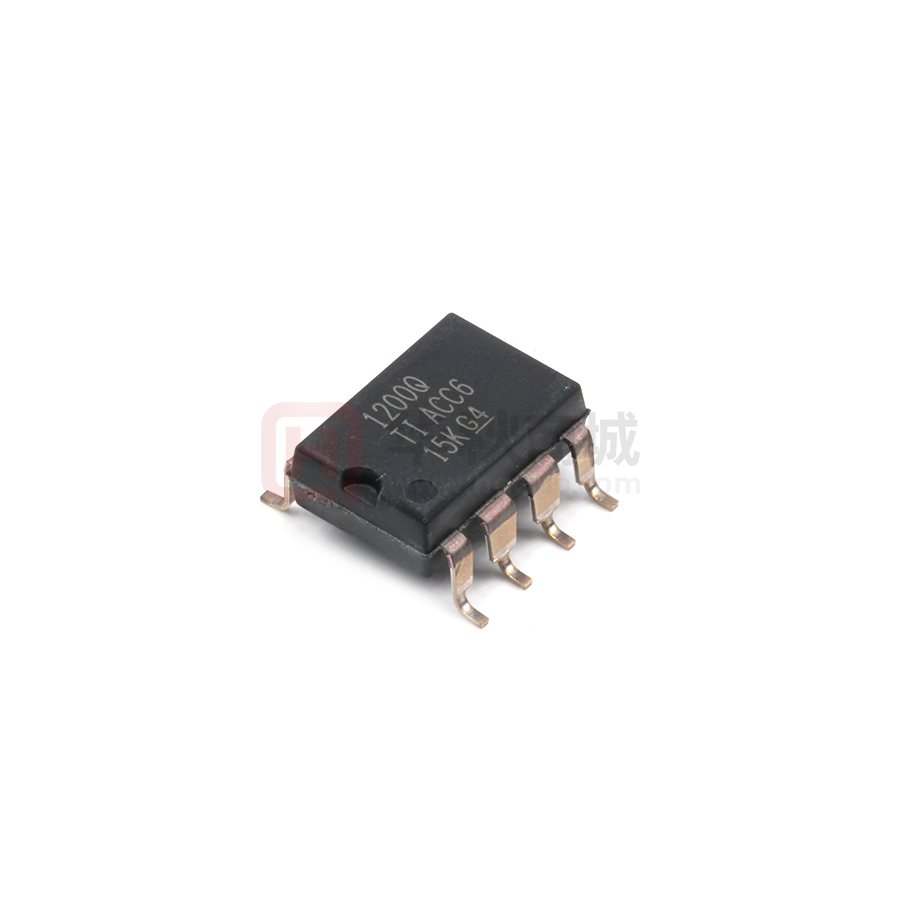
AMC1200STDUBRQ1
ACTIVE
SOP
DUB
8
350
RoHS & Green
NIPDAU
Level-3-260C-168 HR
-40 to 105
1200Q
AMC1200TDWVRQ1
ACTIVE
SOIC
DWV
8
1000
RoHS & Green
NIPDAU
Level-2-260C-1 YEAR
-40 to 105
1200Q
(1)
The marketing status values are defined as follows:
ACTIVE: Product device recommended for new designs.
LIFEBUY: TI has announced that the device will be discontinued, and a lifetime-buy period is in effect.
NRND: Not recommended for new designs. Device is in production to support existing customers, but TI does not recommend using this part in a new design.
PREVIEW: Device has been announced but is not in production. Samples may or may not be available.
OBSOLETE: TI has discontinued the production of the device.
(2)
RoHS: TI defines "RoHS" to mean semiconductor products that are compliant with the current EU RoHS requirements for all 10 RoHS substances, including the requirement that RoHS substance
do not exceed 0.1% by weight in homogeneous materials. Where designed to be soldered at high temperatures, "RoHS" products are suitable for use in specified lead-free processes. TI may
reference these types of products as "Pb-Free".
RoHS Exempt: TI defines "RoHS Exempt" to mean products that contain lead but are compliant with EU RoHS pursuant to a specific EU RoHS exemption.
Green: TI defines "Green" to mean the content of Chlorine (Cl) and Bromine (Br) based flame retardants meet JS709B low halogen requirements of


 工商网监
湘ICP备2023018690号
工商网监
湘ICP备2023018690号

