Sample &
Buy
Product
Folder
Support &
Community
Tools &
Software
Technical
Documents
AMC80
SBOS559B – MAY 2011 – REVISED OCTOBER 2015
AMC80 System Hardware Monitor with Two-Wire and SMBus Serial Interface
1 Features
3 Description
•
•
•
The AMC80 is a system hardware monitoring and
control circuit that includes a seven-channel, 10-bit
analog-to-digital converter (ADC), two programmable
fan-speed monitors, and a two-wire interface. The
AMC80 also includes programmable upper over-limit
and lower under-limit alarms that activate when the
programmed limits are exceeded.
1
•
•
•
•
•
•
•
10-Bit ADC With Seven Analog Inputs
Fan-Speed Monitoring Inputs
Input Range/Resolution:
– Default: 2.56 V/2.5 mV
– Programmable: VDD/6 mV
Chassis Intrusion Detection Input
Interrupt Alarms:
– Upper Over-Limit
– Lower Under-Limit
Interrupt Status Register Input for External
Temperature Sensors
Shutdown Mode
Programmable RST_OUT/OS
Pin Compatible with LM96080 and LM80
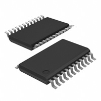
Package: 24-Pin TSSOP
The AMC80 can interface with both linear and digital
temperature sensors. The 2.5-mV least significant bit
(LSB) and 2.56-V input range can accept inputs from
a linear sensor such as the TMP20. The BTI pin is
used as an input from a digital sensor such as the
TMP75. The AMC80 operates from a 3-V to 5.5-V
supply voltage, has low supply current, and can be
configured using a two-wire interface, thus making it
ideal for a wide range of applications.
The AMC80 is available in a 24-lead TSSOP package
and is fully specified over the –40°C to +125°C
temperature range.
2 Applications
•
•
•
•
•
•
Device Information(1)
Communications Equipment
Servers
Industrial and Medical Equipment
Storage Area Networks
Set-Top Boxes
Test and Measurement Equipment
PART NUMBER
AMC80
PACKAGE
TSSOP (24)
BODY SIZE (NOM)
7.80 mm × 4.40 mm
(1) For all available packages, see the package option addendum
at the end of the data sheet.
Simplified Schematic
AMC80
Positive
Voltage
CH0
CH1
CH2
Analog
Inputs
Negative
Voltage
CH3
10-Bit
Delta-Sigma
ADC
CH4
CH5
CH6
Temperature
Sensor
V+
FAN1
TMP75
Temperature
Sensor
Chassis
Intrusion
Detector
FAN2
Limit
Registers
and
Alarm
Comparators
Interrupt
Masking
and
Interrupt
Control
INT
RST_OUT/OS
Interrupt
Outputs
Fan Speed
Counter
BTI
GPI(CI)
INT_IN
SDA
Serial
Bus
Interface
SCL
A0/NTEST_OUT
A1
GPO
Interface and Control
NTEST_IN/RESET_IN
Digital
Inputs
and
Outputs
A2
1
An IMPORTANT NOTICE at the end of this data sheet addresses availability, warranty, changes, use in safety-critical applications,
intellectual property matters and other important disclaimers. PRODUCTION DATA.
�AMC80
SBOS559B – MAY 2011 – REVISED OCTOBER 2015
www.ti.com
Table of Contents
1
2
3
4
5
6
7
Features ..................................................................
Applications ...........................................................
Description .............................................................
Revision History.....................................................
Pin Configuration and Functions .........................
Specifications.........................................................
1
1
1
2
3
5
6.1
6.2
6.3
6.4
6.5
6.6
6.7
5
5
5
5
6
8
9
Absolute Maximum Ratings .....................................
ESD Ratings..............................................................
Recommended Operating Conditions.......................
Thermal Information ..................................................
Electrical Characteristics...........................................
Timing Requirements ................................................
Typical Characteristics ..............................................
Detailed Description ............................................ 10
7.1
7.2
7.3
7.4
7.5
Overview .................................................................
Functional Block Diagram .......................................
Feature Description.................................................
Programming...........................................................
Register Map...........................................................
10
10
10
14
16
8
Application and Implementation ........................ 21
9
Device and Documentation Support.................. 23
8.1 Application Information............................................ 21
9.1
9.2
9.3
9.4
Community Resources............................................
Trademarks .............................................................
Electrostatic Discharge Caution ..............................
Glossary ..................................................................
23
23
23
23
10 Mechanical, Packaging, and Orderable
Information ........................................................... 23
4 Revision History
Changes from Revision A (January 2012) to Revision B
Page
•
Changed INT pin description .................................................................................................................................................. 4
•
Added pins to input voltage range in Absolute Maximum Ratings table ................................................................................ 5
•
Added ESD Ratings table....................................................................................................................................................... 5
•
Added new note 1 to Timing Requirements table .................................................................................................................. 8
•
Added Detailed Description section...................................................................................................................................... 10
•
Added Application and Implementation section.................................................................................................................... 21
•
Added Device and Documentation Support section............................................................................................................. 23
Changes from Original (May 2011) to Revision A
Page
•
Added SMBus timeout parameter to Electrical Characteristics.............................................................................................. 6
•
Changed Bit 0 = '1' in Table 10 ............................................................................................................................................ 18
2
Submit Documentation Feedback
Copyright © 2011–2015, Texas Instruments Incorporated
Product Folder Links: AMC80
�AMC80
www.ti.com
SBOS559B – MAY 2011 – REVISED OCTOBER 2015
5 Pin Configuration and Functions
PW Package
24-Pin TSSOP
Top View
INT_IN
1
24
A2
SDA
2
23
A1
SCL
3
22
A0/NTEST_OUT
FAN1
4
21
CH0
FAN2
5
20
CH1
BTI
6
19
CH2
AMC80
GPI/CI
7
18
CH3
GND
8
17
CH4
V+
9
16
CH5
INT
10
15
CH6
GPO
11
14
AGND
NTEST_IN/RESET_IN
12
13
RST_OUT/OS
Submit Documentation Feedback
Copyright © 2011–2015, Texas Instruments Incorporated
Product Folder Links: AMC80
3
�AMC80
SBOS559B – MAY 2011 – REVISED OCTOBER 2015
www.ti.com
Pin Functions
PIN
NO.
NAME
I/O
TYPE
DESCRIPTION
1
INT_IN
Input
Digital
Interrupt input pin. An active low input that extends the INT_IN signal to the INT output
of the AMC80.
2
SDA
I/O
Digital
Serial bus data line for SMBus, open-drain; requires pull-up resistor.
3
SCL
I/O
Digital
Serial bus clock line for SMBus, open-drain; requires pull-up resistor.
4
FAN1
Input
Digital
Fan tachometer input pin
5
FAN2
Input
Digital
Fan tachometer input pin
6
BTI
Input
Digital
Board temperature interrupt pin. BTI is driven by the over-temperature shutdown (OS)
outputs of the additional temperature sensors. This pin has an internal 10-kΩ pull-up
resistor.
7
GPI(CI)
Input
Digital
General-purpose input pin (chassis interrupt). An active high interrupt input pin to latch
a chassis interrupt event.
8
DGND
Power
Analog
Digital ground.
9
V+
Power
Analog
Positive supply voltage (3V to 5.5V).
10
INT
Output
Digital
Non-maskable interrupt (active high, PMOS, push-pull) or interrupt request (active low,
NMOS, push-pull) pin. The INT pin becomes active when INT_IN, BTI, or GPI
interrupts. This pin does not require a pullup resistor to V+.
11
GPO
Output
Digital
General-purpose output pin. GPO is an active low, NMOS, open-drain output. This pin
is intended to drive an external power PMOS for software power control or to control
power to a cooling fan.
12
NTEST_IN/RESET_IN
Input
Digital
This pin is an active-low input that enables NAND tree board-level connectivity testing.
The AMC80 resets to its power-on state when NAND tree connectivity is enabled.
13
RST_OUT/OS
Output
Digital
This pin is an NMOS open-drain output. RST_OUT provides a master reset to devices
connected to this line. OS is dedicated to the temperature reading alarm.
14
AGND
Power
Analog
Analog ground. This pin must be tied to a low-noise analog ground plane for optimum
performance.
15
CH6
Input
Analog
Analog input channel 6
16
CH5
Input
Analog
Analog input channel 5
17
CH4
Input
Analog
Analog input channel 4
18
CH3
Input
Analog
Analog input channel 3
19
CH2
Input
Analog
Analog input channel 2
20
CH1
Input
Analog
Analog input channel 1
21
CH0
Input
Analog
Analog input channel 0
22
A0/NTEST_OUT
I/O
Digital
The lowest order bit of the serial bus address. During a NAND tree test for ATE boardlevel connectivity, this pin functions as an output.
23
A1
Input
Digital
Address pin 1
24
A2
Input
Digital
Address pin 2
4
Submit Documentation Feedback
Copyright © 2011–2015, Texas Instruments Incorporated
Product Folder Links: AMC80
�AMC80
www.ti.com
SBOS559B – MAY 2011 – REVISED OCTOBER 2015
6 Specifications
6.1 Absolute Maximum Ratings (1)
Over operating free-air temperature range, unless otherwise noted.
MIN
MAX
UNIT
–0.3
7
V
Pins 6, 10, 15, 16, 17, 18, 19, 20, 21, 22, 24
–0.3
(V+) + 0.3
Pins 1, 2, 3, 4, 5, 7, 9, 11, 12, 13, 23
–0.3
7
Power-supply voltage range, V+
Input voltage range, VIN
Input current, IIN
Operating temperature range, TA
–55
Junction temperature range, TJ max
Storage temperature range, TSTG
(1)
–65
V
10
mA
127
°C
150
°C
150
°C
Stresses above these ratings my cause permanent damage. Exposure to absolute maximum conditions for extended periods may
degrade device reliability. These are stress ratings only, and functional operation of the device at these or any other conditions beyond
those specified is not implied.
6.2 ESD Ratings
VALUE
V(ESD)
(1)
(2)
Electrostatic discharge
Human-body model (HBM), per ANSI/ESDA/JEDEC JS-001 (1)
±2500
Charged-device model (CDM), per JEDEC specification JESD22-C101 (2)
±1000
Machine model (MM)
±200
UNIT
V
JEDEC document JEP155 states that 500-V HBM allows safe manufacturing with a standard ESD control process.
JEDEC document JEP157 states that 250-V CDM allows safe manufacturing with a standard ESD control process. ance.
6.3 Recommended Operating Conditions
MIN
Supply voltage range, V+
Input voltage range, VIN
Operating temperature range, TA
NOM
MAX
UNIT
3
5.5
–0.05
(V+) + 0.05
V
V
–40
125
°C
6.4 Thermal Information
AMC80
THERMAL METRIC (1)
PW (TSSOP)
UNIT
24 PINS
RθJA
Junction-to-ambient thermal resistance
100.72
°C/W
RθJC(top)
Junction-to-case (top) thermal resistance
31.4
°C/W
RθJB
Junction-to-board thermal resistance
54.7
°C/W
ψJT
Junction-to-top characterization parameter
1.0
°C/W
ψJB
Junction-to-board characterization parameter
54.2
°C/W
RθJC(bot)
Junction-to-case (bottom) thermal resistance
N/A
°C/W
(1)
For more information about traditional and new thermal metrics, see the Semiconductor and IC Package Thermal Metrics application
report, SPRA953.
Submit Documentation Feedback
Copyright © 2011–2015, Texas Instruments Incorporated
Product Folder Links: AMC80
5
�AMC80
SBOS559B – MAY 2011 – REVISED OCTOBER 2015
www.ti.com
6.5 Electrical Characteristics
At TA –40°C to +125°C and V+ = 3 V to 5.5 V, unless otherwise noted.
PARAMETER
TEST CONDITIONS
MIN
TYP
MAX
UNIT
DIGITAL INPUTS
VIH
Input high voltage
VIL
Input low voltage
VHYS
2
V+ = 3.3 V
Hysteresis voltage
IIH
Input high current
IIL
Input low current
CIN
Input capacitance
V
0.8
0.23
V+ = 5 V
VIH = V+, all pins except BTI
VIH = V+, BTI pin
V
V
0.33
V
–1
–0.005
µA
–10
–1
µA
VIL = 0 V, all pins except BTI
0.005
VIL = 0 V, V+ = 5.5 V, BTI pin
1
µA
2
mA
20
pF
ANALOG INPUTS
Default
0
2.56
Programmable
0
V+
VIN
Input voltage range
IL-ON
Input leakage current (on)
±0.005
IL-OFF
Input leakage current (off)
±0.005
RIN
Input resistance
2
V
V
µA
µA
10
kΩ
DIGITAL OUTPUTS (A0/NTEST_OUT, INT)
VOH
Output high voltage
IOUT = 3 mA/5 mA, V+ = 3 V/4.5 V
VOL
Output low voltage
IOUT = 3 mA/5 mA, V+ = 3 V/4.5 V
2.4
V
0.4
V
DIGITAL OPEN-DRAIN OUTPUTS (GPO, RST_OUT/OS, GPI/CI, SDA)
VOL
Output low voltage
IOUT = 3 mA/5 mA, V+ = 3 V/4.5 V,
all pins except SDA
0.4
IOUT = 4 mA, V+ = 3 V, SDA pin
0.4
IOH
Output high current
VOUT = V+
tw
Pulse duration
RST_OUT/OS, GPI/CI
0.005
10
1
22.5
V
µA
ms
SMBus
SMBus timeout (1)
28
35
ms
TA = –40°C to +125°C
±3
°C
TA = –25°C to +100°C
±2
°C
TEMPERATURE ERROR
TE
Temperature error
TR
Temperature resolution
0.0625
°C
ANALOG-TO-DIGITAL CONVERTER
VR
Resolution
DNL
Differential linearity
ADCERR
Total unadjusted error
VIN = 2.56 V
Power supply rejection ratio
tC (4)
Total conversion time
6
mV
6
–1
(3)
PSRR
(1)
(2)
(3)
(4)
2.5
VIN = V+
1
–1%
LSB (2)
1%
±0.0008
%
662
728
810
ms
The SMBus timeout in the AMC80 resets the interface anytime SCL or SDA is low for over 28 ms.
LSB means least significant bit.
Total unadjusted error contains offset, gain, and linearity errors of the ADC.
Total conversion time contains the temperature conversion, the seven analog input voltage conversions, and the two tachometer
readings.
Submit Documentation Feedback
Copyright © 2011–2015, Texas Instruments Incorporated
Product Folder Links: AMC80
�AMC80
www.ti.com
SBOS559B – MAY 2011 – REVISED OCTOBER 2015
Electrical Characteristics (continued)
At TA –40°C to +125°C and V+ = 3 V to 5.5 V, unless otherwise noted.
PARAMETER
TEST CONDITIONS
MIN
TYP
MAX
UNIT
FAN RPM-TO-DIGITAL CONVERTER
FANERR
Fan RPM error
fCLK
Internal clock frequency
FANRPM
FSC
FAN1 and FAN2 nominal input RPM
–10%
20.2
10%
22.5
Divisor = 1, fan count = 153
8800
Divisor = 2, fan count = 153
4400
Divisor = 3, fan count = 153
2200
Divisor = 4, fan count = 153
1100
Full-scale count
24.8
kHz
RPM
255 Counts
POWER SUPPLY
V+
Specified voltage range
IQA
Quiescent current, average
IQSD
Quiescent current, shutdown mode
3
5.5
V+ = 5.5 V
100
V+ = 3.8 V
25
V+ = 5.5 V
100
V+ = 3.8 V
25
V
µA
µA
TEMPERATURE
TA
Specified range
-40
125
Submit Documentation Feedback
Copyright © 2011–2015, Texas Instruments Incorporated
Product Folder Links: AMC80
°C
7
�AMC80
SBOS559B – MAY 2011 – REVISED OCTOBER 2015
www.ti.com
6.6 Timing Requirements
At TA –40°C to +125°C and VS = 3V to 5.5V, unless otherwise noted.
FAST MODE (1)
HIGH-SPEED MODE (1)
MIN
MAX
MIN
MAX
UNIT
10
400
10
3400
kHz
f(SCL)
SCL operating frequency
t(BUF)
Bus free time between STOP and START conditions
600
160
ns
t(HDSTA)
Hold time after repeated START condition. After this
period, the first clock is generated.
600
160
ns
t(SUSTA)
Repeated START condition setup time
600
160
ns
t(SUSTO)
STOP condition setup time
600
160
ns
(2)
(3)
ns
t(HDDAT)
Data hold time
0
t(SUDAT)
Data setup time
100
10
ns
t(LOW)
Clock low period
1300
160
ns
t(HIGH)
Clock high period
600
60
ns
tR
Clock/Data input rise time
300
160
ns
tF
Clock/Data input fall time
300
160
ns
(1)
(2)
(3)
0
Values based on a statistical analysis of a one-time sample of devices. Minimum and maximum values are not specified and not
production tested.
For cases when the fall time of SCL is less than 20 ns and/or the rise time or fall time of SDA is less than 20 ns, the hold time should be
greater than 20 ns.
For cases when the fall time of SCL is less than 10 ns and/or the rise or fall time of SDA is less than 10 ns, the hold time should be
greater than 10 ns.
t(LOW)
tF
tR
t(HDSTA)
SCL
t(HDSTA)
t(HIGH)
t(HDDAT)
t(SUSTO)
t(SUSTA)
t(SUDAT)
SDA
t(BUF)
P
S
S
P
Figure 1. Serial Bus Interface Timing
8
Submit Documentation Feedback
Copyright © 2011–2015, Texas Instruments Incorporated
Product Folder Links: AMC80
�AMC80
www.ti.com
SBOS559B – MAY 2011 – REVISED OCTOBER 2015
6.7 Typical Characteristics
At TA = +25°C and V+ = 3 V to 5.5 V, unless otherwise noted.
220
50
45
200
40
180
30
IQV (mA)
IQA (mA)
35
25
20
160
140
15
10
120
5
0
100
2.5
3
3.5
4
4.5
5
5.5
3
2.5
3.5
4
4.5
5
5.5
V+ (V)
V+ (V)
Figure 2. Average Quiescent Current vs Supply Voltage
Figure 3. Quiescent Current During Voltage Conversion vs
Supply Voltage
45
240
40
220
35
30
IQSD (mA)
IQT (mA)
200
180
160
25
20
15
140
10
120
5
0
100
2.5
3
3.5
4
4.5
5
2.5
5.5
3
3.5
4
4.5
5
5.5
V+ (V)
V+ (V)
Figure 4. Quiescent Current During Temperature
Conversion vs Supply Voltage
Figure 5. Quiescent Current During Shutdown vs Supply
Voltage
Temperature Error (°C)
0.16
0.12
0.08
0.04
2.5
3
3.5
4
4.5
5
5.5
V+ (V)
Figure 6. Temperature Error vs Supply Voltage
Submit Documentation Feedback
Copyright © 2011–2015, Texas Instruments Incorporated
Product Folder Links: AMC80
9
�AMC80
SBOS559B – MAY 2011 – REVISED OCTOBER 2015
www.ti.com
7 Detailed Description
7.1 Overview
The AMC80 provides seven analog inputs, a temperature sensor, a delta-sigma analog-to-digital converter
(ADC), and a variety of inputs and outputs on a single chip. A two-wire SMBus interface is also provided. The
AMC80 can continuously perform power-supply, temperature, and fan monitoring for a variety of applications.
The AMC80 is fully pin- and software-compatible with the LM96080 and LM80.
7.2 Functional Block Diagram
AMC80
CH0
CH1
Analog
Inputs
CH2
CH3
CH4
CH5
CH6
10-Bit
Delta-Sigma
ADC
Temperature
Sensor
Fan
Tachometer
Pulse Inputs
FAN1
FAN2
Value RAM
Watchdog
IN0
Addr = 20h
IN1
Addr = 21h
IN2
Addr = 22h
IN3
Addr = 23h
IN4
Addr = 24h
IN5
Addr = 25h
IN6
Addr = 26h
Upper Limit
Lower Limit
Upper Limit
Lower Limit
Upper Limit
Lower Limit
Upper Limit
Lower Limit
Upper Limit
Lower Limit
Upper Limit
Lower Limit
Upper Limit
Lower Limit
OS
Hysteresis
Hot
Hysteresis
Temperature
Addr = 27h
Fan Speed
Counter
Fan1
Addr = 28h
Fan2
Addr = 29h
Interrupt
Status
Registers
INT
Interrupt
Masking
and
Interrupt
Control
Interrupt
Outputs
RST_OUT/OS
Upper Limit
Upper Limit
BTI
GPI(CI)
INT_IN
SDA
Serial
Bus
Interface
SCL
A0/TEST_OUT
GPO
Interface and Control
A1
NTEST_IN/RESET_IN
A2
Digital
Inputs
and
Outputs
7.3 Feature Description
7.3.1 Block Level Description
The AMC80 continuously converts analog inputs to 10-bit resolution using a 2.5-mV least significant bit (LSB)
with a default input range of 0 V to 2.56 V, or a 6-mV LSB with a programmable input range of 0 V to V+. The
analog inputs (CH0 to CH6) are intended for connection to the several power supplies present in any typical
system. Temperature can be converted to a 9-bit or 12-bit resolution with either 0.5°C or 0.0625°C LSB,
respectively. The FAN1 and FAN2 inputs can be programmed to accept either a fan failure indicator or
tachometer signals. Fan failure signals can be programmed to be either active high or active low. Fan inputs
measure the period of tachometer pulses from the the fans, providing a higher count for lower fan speeds. The
fan inputs are digital inputs with transition levels according to the Digital Inputs section of the Electrical
Characteristics table. Full-scale fan counts are 255 (8-bit counter), which represent a stopped or very slow fan.
Nominal speeds, based on a count of 153, are programmable from 1100 RPM to 8800 RPM. Signal conditioning
circuitry is included to accommodate slow rise and fall times.
The AMC80 provides a number of internal registers:
• Configuration Register: Provides control and configuration.
• Interrupt Status Registers: Two registers that provide the status of each interrupt alarm.
• Interrupt Mask Registers: Allows masking of individual interrupt sources, as well as separate masking for
10
Submit Documentation Feedback
Copyright © 2011–2015, Texas Instruments Incorporated
Product Folder Links: AMC80
�AMC80
www.ti.com
SBOS559B – MAY 2011 – REVISED OCTOBER 2015
Feature Description (continued)
•
•
•
•
•
•
•
•
both hardware interrupt outputs.
Fan Divisor/RST_OUT/OS Register: Bits 0 to 5 of this register contain the divisor bits for the FAN1 and
FAN2 inputs. Bits 6 and 7 control the function of the RST_OUT/OS output.
OS Configuration/Temperature Resolution Register: The configuration of the overtemperature shutdown
(OS) is controlled by the lower three bits of this register. Bit 3 enables 12-bit temperature conversions. In 12bit mode, bits 4 to 7 represent the four LSBs of the temperature measurement. In 9-bit mode, bit 4 represents
the LSB of the temperature measurement.
Conversion Rate Register: Sets the time interval of the continuous monitoring cycle to either fixed or
programmable (see the Conversion Rate Count Register for setting the programmable time interval).
Voltage/Temperature Channel Disable Register: Allows voltage inputs and the local temperature
conversion to be disabled.
Input Mode Register: Allows voltage inputs to be configured as single-ended or as a differential pair with
normal or reverse polarity.
ADC Control Register: Bits 0 to 2 set the programmable conversion rate for the 10-bit ADC. Bits 3 to 5 allow
for programmable input full-scale voltage.
Conversion Rate Count Register: Selects the adjustable time interval when the conversion rate of the
continuous monitoring cycle is set to programmable.
Value RAM: The monitoring results (for temperature, voltages, fan counts, and Fan Divisor/RST_OUT/OS
Register limits) are all contained in the Value RAM. The Value RAM consists of 32 bytes. The first 10 bytes
are all of the results, the next 20 bytes are the interrupt alarm limits, and the last two bytes are at the upper
locations for manufacturer ID and die revision ID.
The AMC80 SMBus is compatible with both fast mode (400 kHz) and high-speed mode (3.4 MHz) two-wire
interface modes of operation. The AMC80 supports a timeout reset function on SDA and SCL that prevents twowire bus lockup, and includes an analog filter on the two-wire digital control lines that improves noise immunity.
Three address pins (A0 to A2), allow up to eight devices on a single bus. When enabled, the AMC80 starts by
cycling through each measurement in sequence, and continuously loops through the sequence based on the
Conversion Rate Register (address 07h) setting. Each measured value is compared to values stored in the Value
RAM Registers (addresses 2Ah to 3Dh). When the measured value exceeds the programmed limit, the AMC80
sets a corresponding interrupt in the Interrupt Status Registers (addresses 01h and 02h). Two output interrupt
lines (INT and RST_OUT/OS) are available. INT is fully programmable with the ability to mask each interrupt
source and each output. The Fan Divisor/RST_OUT/OS Register (address 05h) has control bits that enable or
disable the hardware interrupts. Additional digital inputs are provided for daisy-chaining the interrupt output pin,
INT. This configuration is achieved by connecting multiple external temperature sensors (for example, the
TMP75) to the board temperature interrupt (BTI) input and/or the GPI/CI input. The chassis intrusion (CI) input is
designed to accept an active high signal from an external circuit that latches (for example, when the chassis from
a server rack is removed).
Submit Documentation Feedback
Copyright © 2011–2015, Texas Instruments Incorporated
Product Folder Links: AMC80
11
�AMC80
SBOS559B – MAY 2011 – REVISED OCTOBER 2015
www.ti.com
Feature Description (continued)
7.3.2 Temperature Measurement
The AMC80 ΔVBE-type temperature sensor, is a ΔΣ ADC that performs 9-bit or 12-bit twos complement
temperature conversions. An 8-bit comparator that compares the readings to the user-programmable hot and
overtemperature setpoints, and hysteresis values is also incorporated into the AMC80.
Temperature data can be read from the Temperature Reading Register (address 27h). Temperature limits can be
read from and written to the Hot Temperature (THOT), Hot Temperature Hysteresis (THOT_HYST), OS Temperature
(TOS), and OS Temperature Hysteresis (TOS_HYST) Limit Registers (addresses 38h to 3Bh). Each limit is
represented in 12-bit, 9-bit, or 8-bit resolution, as shown in Table 1.
Table 1. Temperature Lookup
TEMPERATURE
12-BIT DIGITAL OUTPUT (HEX)
LSB = 0.0625°C
9-BIT DIGITAL OUTPUT (HEX)
LSB = 0.5°C
8-BIT DIGITAL OUTPUT (HEX)
LSB = 1°C
+125°C
07D
0FA
7D
+25°C
019
032
19
+1°C
010
003
01
0.0625°C
001
—
—
0°C
000
000
00
–0.0625°C
FFF
—
—
FF
–1°C
FF0
1FF
–25°C
E70
1CE
E7
–55°C
C90
192
C9
When using a single-byte read, the eight MSBs of the temperature reading can be found in the Value RAM
Register (address 27h). The remainder of the temperature reading can be found in the OS
Configuration/Temperature Resolution Register (address 06h), bits 4 to 7. In 9-bit format, bit 7 is the only valid
bit. In addition, all nine or 12 bits can be read using a double-byte read at register address 27h.
There are four Value RAM Register limits for the temperature reading that affect the INT and OS outputs of the
AMC80. These are the THOT, THOT_HYST, TOS, TOS_HYST Limit Registers (addresses 38h to 3Bh); see Table 15.
There are three interrupt modes of operation: Default Interrupt, One-Time Interrupt, and Comparator. The OS
output of the AMC80 can be programmed for One-Time Interrupt mode and Comparator mode. INT can be
programmed for Default Interrupt mode and One-Time Interrupt mode. These modes are explained in the
following subsections.
7.3.2.1 Default Interrupt Mode
In Default Interrupt mode, exceeding THOT causes an interrupt that remains active indefinitely until reset by
reading Interrupt Status Register 1 (address 01h) or cleared by the INT_Clear bit in the Configuration Register
(address 00h, bit 3). When an interrupt event has occurred by exceeding THOT, and is then reset, another
interrupt occurs again when the next temperature conversion has completed. The interrupts continue to occur in
this manner until the temperature falls below THOT_HYST, at which time the interrupt output automatically clears.
7.3.2.2 One-Time Interrupt Mode
In One-Time Interrupt mode, exceeding THOT causes an interrupt that remains active indefinitely until reset by
reading Interrupt Status Register 1 or cleared by the INT_Clear bit in the Configuration Register. When an
interrupt event has occurred by exceeding THOT, and is then reset, an interrupt does not occur again until the
temperature falls below THOT_HYST.
7.3.2.3 Comparator Mode
In Comparator mode, exceeding TOS causes the OS output to go low (default) and remain low until the
temperature falls below TOS_HYST. When the temperature falls below TOS_HYST, OS goes high.
12
Submit Documentation Feedback
Copyright © 2011–2015, Texas Instruments Incorporated
Product Folder Links: AMC80
�AMC80
www.ti.com
SBOS559B – MAY 2011 – REVISED OCTOBER 2015
7.3.3 Interrupt Structure
Figure 7 depicts the interrupt structure of the AMC80.
OS Status: R06h, B0
Temp Watchdog
OS Polarity: R06h, B1
Input,
Temperature,
and Fan
Watchdogs
Interrupt
Status
Registers
OS Pin Enable: R05h, B6
RST_OUT/OS
RST Enable: R05h, B7
Interrupt
Masking
and
Control
RESET: R00h, B4
INT
BTI
GPI/CI
INT_IN
INT Enable: R00h, B1
INT Clear: R00h, B3
INT Polarity Select: R00h, B2
Figure 7. Interrupt Structure
External interrupt inputs can come from the following sources:
• Board Temperature Interrupt (BTI) - This pin is an active low interrupt recommended to come from the
overtemperature shutdown (OS) output of TMP75 temperature sensors. The TMP75 OS output activates
when its temperature exceeds a programmed threshold. If the temperature of any TMP75 exceeds its
programmed limit, BTI is driven low. This action generates an interrupt through bit 1 of Interrupt Status
Register 2 (address 02h) that notifies the host of a possible overtemperature condition. To disable this
feature, set bit 1 of Interrupt Mask Register 2 (address 04h) to high. This pin also provides an internal, 10-kΩ
pull-up resistor.
• GPI/CI - This pin is an active high interrupt from any type of device that detects and captures chassis
intrusion violations. This action could be accomplished mechanically, optically, or electrically; circuitry external
to the AMC80 is expected to latch the event. Read this interrupt using bit 4 of Interrupt Status Register 2
(address 02h), and disable it using bit 4 of Interrupt Mask Register 2 (address 04h). The design of the AMC80
allows this input to go high even with no power applied, and no clamping or other interference with the line
occurs. This line can also be pulled low by the AMC80 for at least 10ms to reset a typical chassis-intrusion
circuit. Accomplish this reset by setting bit 5 of the Configuration Register (address 00h) to high; this bit is
self-clearing.
• INT_IN - This pin is an active low interrupt that provides a way to connect an INT from other devices through
the AMC80 to the processor. If this pin is pulled low, then bit 7 of Interrupt Status Register 1 (address 01h)
goes high, indicating this interrupt detection. Setting bit 1 of the Configuration Register (address 00h) also
allows the INT pin to go low when INT_IN goes low. To disable this feature, set bit 7 of Interrupt Mask
Register 1 (address 03h) to high.
Device interrupt outputs can come from the following sources:
• INT - This pin becomes active whenever INT_IN, BTI, or GPI/CI interrupts. INT is enabled when bit 1 of the
Configuration Register (address 00h) is set high. Bits 2 and 3 of the Configuration Register are also used to
set the polarity and state of the INT interrupt line.
• OS - In the Fan Divisor/RST_OUT/OS Register (address 05h), bit 6 (OS Pin Enable), must be set high and bit
7 (RST Enable) must be set to low in order to enable the OS function on the RST_OUT/OS pin. The OS pin
has two modes of operation: One-Time Interrupt and Comparator. One-Time Interrupt mode is selected by
taking bit 2 of the OS Configuration/Temperature Resolution Register (address 06h) high. If bit 2 is taken low,
then Comparator mode is selected. Unlike the OS pin, the OS bit in Interrupt Status Register 2 (address 02h,
bit 5) functions in Default Interrupt and One-Time Interrupt modes. The OS bit can be masked to the INT pin
by taking bit 5 in Interrupt Mask Register 2 (address 04h) low.
Reading the Interrupt Status Registers (addresses 01h to 02h) outputs the contents and then resets the registers
and the INT pin. The INT pin is also cleared by the INT_Clear bit (address 00h, bit 3) without affecting the
contents of the Interrupt Status Registers. When this bit is high, the AMC80 monitoring loop is inactive;
monitoring resumes when this bit is low.
Submit Documentation Feedback
Copyright © 2011–2015, Texas Instruments Incorporated
Product Folder Links: AMC80
13
�AMC80
SBOS559B – MAY 2011 – REVISED OCTOBER 2015
www.ti.com
7.4 Programming
7.4.1 Interface and Control
The SMBus control lines in the AMC80 include SDA, SCL, and the A0 to A2 address pins, which allow up to
eight AMC80 devices to be on the same bus. The AMC80 can only operate as a slave device. The SCL line
controls only the serial interface; all other clock-related functions within the AMC80 (such as the ADC and fan
counters) operate with a separate asynchronous internal clock. The default power-on SMBus address for the
AMC80 is '0101'(A2)(A1)(A0) binary, where (A2)(A1)(A0) is the SMBus address.
When using the SMBus interface, a write command always consists of the AMC80 SMBus interface address
byte, followed by the internal address register byte, and then the data byte (see Figure 8).
See Figure 9 for the read operation timing. There are two cases for a read operation:
1. If the contents of the Internal Address Register are known, simply read the AMC80 with the SMBus interface
address byte, followed by the data byte read from the ADC80.
2. If the internal Address Register contents are unknown, write to the AMC80 with the SMBus interface address
byte, followed by the internal address register bye. Then restart the serial communication with a read that
consist of the SMBus interface address byte, followed by the data byte read from the AMC80.
Table 2. Register Overview
INTERNAL
ADDRESS
(HEX)
POWER-ON
VALUE
(HEX)
Configuration Register
00
08
Interrupt Status Register 1
01
xx
Indeterminate
Interrupt Status Register 2
02
xx
Indeterminate
Interrupt Mask Register 1
03
00
Interrupt Mask Register 2
04
00
Fan Divisor/RST_OUT/OS Register
05
14
FAN1 and FAN2 divisor = 2 (count of 153 = 4400 RPM)
OS Configuration/Temperature Resolution
Register
06
x1
Four MSBs are indeterminate
Conversion Rate Register
07
40
Voltage/Temperature Channel Disable
Register
08
00
Input Mode Register
09
00
ADC Control Register
0A
02
Conversion Rate Count Register
0B
40
Value RAM Register
20 to 29
xx
Indeterminate
Value RAM Register
2A to 3D
xx
Indeterminate
Value RAM Register
3E
80
Value RAM Register
3F
09
REGISTER
14
NOTES
Allows voltage monitoring inputs to be disabled
Submit Documentation Feedback
Copyright © 2011–2015, Texas Instruments Incorporated
Product Folder Links: AMC80
�AMC80
www.ti.com
SBOS559B – MAY 2011 – REVISED OCTOBER 2015
1
9
1
9
SCL
¼
0
SDA
1
0
1
A1(1)
A2(1)
A0(1)
P7
R/W
Start By
Master
P6
P5
P4
P3
P2
P1
P0
ACK By
AMC80
¼
ACK By
AMC80
Frame 2 Pointer Register Byte
Frame 1 Two-Wire Slave Address Byte
1
9
1
9
SCL
(Continued)
SDA
(Continued)
D6
D7
D5
D4
D3
D2
D1
D7
D0
D6
D5
D4
D3
D2
D1
Stop By
Master
Frame 4 Data Byte 2
Frame 3 Data Byte 1
(1)
D0
ACK By
AMC80
ACK By
AMC80
The values of A0, A1, and A2 are determined by the A0, A1, and A2 pins, respectively.
Figure 8. Two-Wire Timing for Write Word Format
1
9
1
9
SCL
¼
SDA
0
1
0
1
A2
(1)
A1
(1)
A0
(1)
P7
R/W
Start By
Master
P6
P5
P4
P3
P2
P1
P0
ACK By
AMC80
ACK By
AMC80
Frame 1 Two-Wire Slave Address Byte
Stop By
Master
Frame 2 Pointer Register Byte
1
9
1
9
SCL
(Continued)
¼
SDA
(Continued)
0
1
0
1
A2
(1)
A1
(1)
A0
(1)
D7
R/W
Start By
Master
D6
D5
D4
D3
ACK By
AMC80
Frame 3 Two-Wire Slave Address Byte
1
D2
D1
D0
From
AMC80
¼
ACK By
Master
(2)
Frame 4 Data Byte 1 Read Register
9
SCL
(Continued)
SDA
(Continued)
D7
D6
D5
D4
D3
D2
D1
D0
ACK By
From
AMC80
Master
(3)
Stop By
Master
Frame 5 Data Byte 2 Read Register
(1)
The values of A0, A1, and A2 are determined by the A0, A1, and A2 pins, respectively.
(2)
Master should leave SDA high to terminate a single-byte read operation.
(3)
Master should leave SDA high to terminate a two-byte read operation.
Figure 9. Two-Wire Timing for Read Word Format
Submit Documentation Feedback
Copyright © 2011–2015, Texas Instruments Incorporated
Product Folder Links: AMC80
15
�AMC80
SBOS559B – MAY 2011 – REVISED OCTOBER 2015
www.ti.com
7.5 Register Map
7.5.1 Configuration Register
Table 3. Configuration Register (Address = 00h, Default = 08h)
BIT
NAME
TYPE
DESCRIPTION
0
Start
R/W
'1' enables startup of monitoring activity; '0' puts device in shutdown mode.
1
INT Enable
R/W
'1' enables the INT output.
2
INT Polarity Select
R/W
'1' selects active-high, open-source output; '0' selects active-low, open-drain output.
3
INT_Clear
R/W
'1' disables the INT output without affecting the contents of the Interrupt Status Registers.
The device stops monitoring and resumes on a '0'.
4
RESET
R/W
'1' outputs an active-low reset signal at RST_OUT, if bit 7 and bit 6 in the Fan Divisor/
Register (address 05h) are set to '1' and '0', respectively. This bit is cleared when the pulse
becomes inactive.
5
Chassis Clear
R/W
'1' clears the GPI/CI pin. This bit clears itself after 10ms.
6
GPO
R/W
'1' drives the GPO pin low.
7
INITIALIZATION
R/W
'1' restores power-on-default values to the registers. This bit is self-clearing
7.5.2 Interrupt Status Registers
Table 4. Interrupt Status Register 1 (Address = 01h, Default = xxh; see Table 2)
BIT
NAME
TYPE
DESCRIPTION
0
CH0
Read
'1' indicates a high or low limit has been exceeded.
1
CH1
Read
'1' indicates a high or low limit has been exceeded.
2
CH2
Read
'1' indicates a high or low limit has been exceeded.
3
CH3
Read
'1' indicates a high or low limit has been exceeded.
4
CH4
Read
'1' indicates a high or low limit has been exceeded.
5
CH5
Read
'1' indicates a high or low limit has been exceeded.
6
CH6
Read
'1' indicates a high or low limit has been exceeded.
7
INT_IN
Read
'1' indicates that a low signal has been detected on the INT_IN pin.
Table 5. Interrupt Status Register 2 (Address = 02h, Default = xxh; see Table 2)
BIT
16
NAME
TYPE
DESCRIPTION
0
Hot Temperature
Read
'1' indicates a high or low limit has been exceeded. One-Time Interrupt and Default Interrupt
modes are supported and can be set by bit 6 of Interrupt Mask Register 2 (address 04h).
1
BTI
Read
'1' indicates that an interrupt has occurred from the BTI input pin.
2
FAN 1
Read
'1' indicates that a fan count limit has been exceeded.
3
FAN 2
Read
'1' indicates that a fan count limit has been exceeded.
4
GPI/CI
Read
'1' indidates that GPI/CI has gone high.
5
OS
Read
'1' indicates a high or low temperature limit has been exceeded. One-Time Interrupt and
Default Interrupt modes are supported and can be set by bit 7 of Interrupt Mask Register 2
(address 04h).
6
Reserved
Read
This bit is reserved.
7
Reserved
Read
This bit is reserved.
Submit Documentation Feedback
Copyright © 2011–2015, Texas Instruments Incorporated
Product Folder Links: AMC80
�AMC80
www.ti.com
SBOS559B – MAY 2011 – REVISED OCTOBER 2015
7.5.3 Interrupt Mask Registers
Table 6. Interrupt Mask Register 1 (Address = 03h, Default = 00h)
BIT
NAME
TYPE
0
CH0
R/W
1
CH1
R/W
2
CH2
R/W
3
CH3
R/W
4
CH4
R/W
5
CH5
R/W
6
CH6
R/W
7
INT_IN
R/W
DESCRIPTION
'1' disables the corresponding interrupt status bit in Table 4 to trigger the INT interrupt.
Table 7. Interrupt Mask Register 2 (Address = 04h, Default = 00h)
BIT
NAME
TYPE
DESCRIPTION
0
Hot Temperature
R/W
1
BTI
R/W
2
FAN 1
R/W
3
FAN 2
R/W
4
GPI/CI
R/W
5
OS
R/W
6
INT Interrupt Mode
Select
R/W
'0' selects Default Interrupt mode. '1' selects One-Time Interrupt mode.
7
OS Interrupt Mode
Select
R/W
'0' selects Comparator mode. '1' selects One-Time Interrupt mode.
'1' disables the corresponding interrupt status bit in Table 5 to trigger the INT interrupt.
7.5.4 Fan Divisor/RST_OUT/OS Register
Table 8. Fan Divisor/RST_OUT/OS Register (Address = 05h, Default = 14h)
BIT
NAME
TYPE
DESCRIPTION
0
FAN1 Mode Select
R/W
'1' selects the level-sensitive input mode. '0' selects the fan count mode for the FAN1 input.
1
FAN2 Mode Select
R/W
'1' selects the level-sensitive input mode. '0' selects the fan count mode for the FAN2 input.
2
FAN1 RPM Control 1
R/W
3
FAN1 RPM Control 0
R/W
FAN1 speed control:
'00' = divide by 1.
'01' = divide by 2.
'10' = divide by 4.
'11' = divide by 8.
If level-sensitive input is selected, '01' selects an active-low input and '00' selects an activehigh input.
4
FAN2 RPM Control 1
R/W
5
FAN2 RPM Control 0
R/W
6
OS Pin Enable
R/W
'1' enables OS mode on the RST_OUT/OS pin when bit 7 is set to '0'.
NOTE: When bits 6 and 7 are both set to '1', the RST_OUT/OS pin is disabled.
7
RST_OUT Pin Enable
R/W
'1' enables RST_OUT mode on the RST_OUT/OS pin when bit 6 is set to '0'.
NOTE: When bits 6 and 7 are both set to '1', the RST_OUT/OS pin is disabled.
FAN2 speed control:
'00' = divide by 1.
'01' = divide by 2.
'10' = divide by 4.
'11' = divide by 8.
If level select input is selected, '01' selects an active-low input and '00' selects an active-high
input.
Submit Documentation Feedback
Copyright © 2011–2015, Texas Instruments Incorporated
Product Folder Links: AMC80
17
�AMC80
SBOS559B – MAY 2011 – REVISED OCTOBER 2015
www.ti.com
7.5.5 OS Configuration/Temperature Resolution Register
Table 9. OS Configuration/Temperature Resolution Register (Address = 06h, Default = x1h; see Table 2)
BIT
NAME
TYPE
DESCRIPTION
0
OS Status
Read
This bit mirrors the state of the RST_OUT/OS pin when in OS mode.
1
OS Polarity
R/W
'1' selects OS to be active-high '0' selects OS to be active-low.
2
OS Mode Select
R/W
'1' selects One-Time-Interrupt mode; '0' selects Comparator mode.
3
Temperature
Resolution Control
R/W
'1' selects 11-bit plus sign resolution temperature conversion; '0' selects the default 8-bit plus
sign resolution temperature conversion.
4
Temp3
R/W
5
Temp2
R/W
6
Temp1
R/W
7
Temp0
R/W
The lower four LSBs of the 11-bit plus sign temperature data. For 8-bit plus sign temperature
data, bit 7 is the LSB and bits 4 to 6 are undefined.
7.5.6 Conversion Rate Register
Table 10. Conversion Rate Register (Address = 07h, Default = 40h)
BIT
NAME
TYPE
DESCRIPTION
Controls conversion rate:
'0' = Programmable conversion rate by the following formula:
Monitoring delay = (ms) = 1.42 × (8 × N + 6)
where N can be set by bits 7:0 in the Conversion Rate Count Register (address 0Bh).
0
CR1
R/W
1
Reserved
R/W
'0' must be written to this bit.
2
Reserved
R/W
'0' must be written to this bit.
3
Reserved
R/W
'0' must be written to this bit.
4
Reserved
R/W
'0' must be written to this bit.
5
Reserved
R/W
'0' must be written to this bit.
6
Reserved
R/W
'0' must be written to this bit.
7
Reserved
R/W
'0' must be written to this bit.
'1' = Continuous conversion.
7.5.7 Voltage/Temperature Channel Disable Register
Table 11. Voltage/Temperature Channel Disable Register (Address = 08h, Default = 00h)
BIT
18
TYPE
DESCRIPTION
0
CH0
NAME
R/W
'1' disables conversions and suppresses error events; Value RAM Register reads '0' for CH0.
1
CH1
R/W
'1' disables conversions and suppresses error events; Value RAM Register reads '0' for CH1.
2
CH2
R/W
'1' disables conversions and suppresses error events; Value RAM Register reads '0' for CH2.
3
CH3
R/W
'1' disables conversions and suppresses error events; Value RAM Register reads '0' for CH3.
4
CH4
R/W
'1' disables conversions and suppresses error events; Value RAM Register reads '0' for CH4.
5
CH5
R/W
'1' disables conversions and suppresses error events; Value RAM Register reads '0' for CH5.
6
CH6
R/W
'1' disables conversions and suppresses error events; Value RAM Register reads '0' for CH6.
7
Temp
R/W
'1' disables conversions and suppresses error events; Value RAM Register reads '0' for
temperature.
Submit Documentation Feedback
Copyright © 2011–2015, Texas Instruments Incorporated
Product Folder Links: AMC80
�AMC80
www.ti.com
SBOS559B – MAY 2011 – REVISED OCTOBER 2015
7.5.8 Input Mode Register
Table 12. Input Mode Register (Address = 09h, Default = 00h)
BIT
NAME
TYPE
DESCRIPTION
0
Diff01
R/W
When set to '1', CH0 and CH1 operate as a differential input.
When set to '0', CH0 and CH1 operate as 2 single-ended inputs.
1
Pol01
R/W
When bit 0 = '1', CH0 and CH1 differential inputs are setup in normal polarity mode when
this bit is set to '1', and in reverse polarity mode when this bit is set to '0'.
When bit 0 is set to “0”, this bit is ignored.
2
Diff23
R/W
When set to '1', CH2 and CH3 operate as a differential input.
When set to '0', CH2 and CH3 operate as 2 single-ended inputs.
3
Pol23
R/W
When bit 0 = '1', CH2 and CH3 differential inputs are setup in normal polarity mode when
this bit is set to '1', and in reverse polarity mode when this bit is set to '0'.
When bit 0 is set to “0”, this bit is ignored.
4
Diff45
R/W
When set to '1', CH4 and CH5 operate as a differential input.
When set to '0', CH4 and CH5 operate as 2 single-ended inputs.
5
Pol45
R/W
When bit 0 = '1', CH4 and CH5 differential inputs are setup in normal polarity mode when
this bit is set to '1', and in reverse polarity mode when this bit is set to '0'.
When bit 0 is set to “0”, this bit is ignored.
6
Reserved
R/W
'0' must be written to this bit.
7
Reserved
R/W
'0' must be written to this bit.
7.5.9 ADC Control Register
Table 13. ADC Control Register (Address = 0Ah, Default = 02h)
BIT
NAME
TYPE
DESCRIPTION
0
DR2
R/W
The 10-bit ADC conversion rate for the analog inputs is set as follows:
000 = 0.512 kHz
001 = 1 kHz
010 = 1.98 kHz
011 = 3.6 kHz
100 = 6.3 kHz
101 = 9.8 kHz
110 = 13.15 kHz
111 = 13.15 kHz
1
DR1
R/W
2
DR0
R/W
3
PGA2
R/W
4
PGA1
R/W
5
PGA0
R/W
6
Reserved
R/W
'0' must be written to this bit.
7
Reserved
R/W
'0' must be written to this bit.
The full-scale analog input range is set as follows:
000 = 2.56 V
001 = VDD
010 = 4.096 V or VDD (whichever is less)
011 = 2.048 V
100 = 1.024 V
101 = 0.512 V
110 = 0.256 V
111 = 0.256 V
Submit Documentation Feedback
Copyright © 2011–2015, Texas Instruments Incorporated
Product Folder Links: AMC80
19
�AMC80
SBOS559B – MAY 2011 – REVISED OCTOBER 2015
www.ti.com
7.5.10 Conversion Rate Count Register
Table 14. Conversion Rate Count Register (Address = 0Bh, Default = 40h)
BIT
NAME
TYPE
0
CRC7
R/W
1
CRC6
R/W
2
CRC5
R/W
3
CRC4
R/W
4
CRC3
R/W
5
CRC2
R/W
6
CRC1
R/W
7
CRC0
R/W
DESCRIPTION
When bit 0 of the Conversion Rate Register (address 07h) is set to '0', the monitoring
conversion delay can be programmed as follows:
0000000 = 0
0000001 = 1
0000010 = 2
………
1111111 = 255
When bit 0 of the Conversion Rate Register is set to '1', these bits are ignored.
7.5.11 Value Ram Register
Table 15. Value RAM Register (Addresses = 20h to 3Fh)
ADDRESS (HEX)
20
DESCRIPTION
20
CH0 reading (10-bit)
21
CH1 reading (10-bit)
22
CH2 reading (10-bit)
23
CH3 reading (10-bit)
24
CH4 reading (10-bit)
25
CH5 reading (10-bit)
26
CH6 reading (10-bit)
27
Temperature reading (9-bit or 12-bit for easy readback)
28
FAN1 reading
29
FAN2 reading
2A
CH0 high limit
2B
CH0 low limit
2C
CH1 high limit
2D
CH1 low limit
2E
CH2 high limit
2F
CH2 low limit
30
CH3 high limit
31
CH3 low limit
32
CH4 high limit
33
CH4 low limit
34
CH5 high limit
35
CH5 low limit
36
CH6 high limit
37
CH6 low limit
38
Hot temperature high limit (THOT)
39
Hot temperature hysteresis low limit (THOT_HYST)
3A
OS temperature high limit (TOS)
3B
OS temperature hysteresis low limit (TOS_HYST)
3C
FAN1 fan count limit
3D
FAN2 fan count limit
3E
Manufacturer ID (always defaults to 80h)
3F
Die revision ID (always defaults to 08h)
Submit Documentation Feedback
Copyright © 2011–2015, Texas Instruments Incorporated
Product Folder Links: AMC80
�AMC80
www.ti.com
SBOS559B – MAY 2011 – REVISED OCTOBER 2015
8 Application and Implementation
NOTE
Information in the following applications sections is not part of the TI component
specification, and TI does not warrant its accuracy or completeness. TI’s customers are
responsible for determining suitability of components for their purposes. Customers should
validate and test their design implementation to confirm system functionality.
8.1 Application Information
8.1.1 Device Power-On
The AMC80 undergoes a power-on-reset condition when power is first applied to the device, or when the
Configuration Register INITIALIZATION bit (address 00h, bit 7) is set high; this bit automatically clears after
being set. The AMC80 can also be forced to a reset condition by taking the NTEST_IN/RESET_IN pin low for at
least 50 ns.
To start the AMC80 monitoring functions (temperature, analog inputs, and fan speeds), write to the Configuration
Register with a '0' to INT_Clear (bit 3) and a '1' to Start (bit 0). The AMC80 then performs continuous monitoring
of all temperature, analog inputs, and fan speeds. The sequence of items that are monitored (except for the
temperature reading) corresponds to locations in the Value RAM, respectively:
1. Temperature
2. CH0
3. CH1
4. CH2
5. CH3
6. CH4
7. CH5
8. CH6
9. Fan 1
10. Fan 2
The conversion results are available in the Value RAM (addresses 20h to 29h). Conversions can be read at any
time and provide the result of the last conversion. A typical sequence of events after AMC80 power-on consists
of these actions:
1. Set alarm limits
2. Set interrupt masks
3. Start the AMC80 monitoring process
Submit Documentation Feedback
Copyright © 2011–2015, Texas Instruments Incorporated
Product Folder Links: AMC80
21
�AMC80
SBOS559B – MAY 2011 – REVISED OCTOBER 2015
www.ti.com
Application Information (continued)
8.1.2 Analog Inputs
In the default state, the 10-bit ADC has a 2.5-mV LSB, yielding a 2.56-V full-scale input range. The input range
can also be programmed with several values up to the V+ full-scale input range with a 6-mV LSB. These settings
are programmed by bits 3 to 5 in the ADC Control Register.
In most applications, the analog inputs are often connected to power supplies. The voltage inputs should be
attenuated with external resistors to any desired value within the input range.
CAUTION
Care should be taken not to exceed V+ on the device input pins at any time.
In select applications where inputs to be monitored are differential in nature, analog inputs (CH0 to CH5) can be
configured as up to three differential pairs (inputs 0-1, 2-3, and 4-5) by setting bits 0, 2, and 4 in the Input Mode
Register. If needed, the input pair polarity can be changed by setting bits 1, 3, and 5 in the Input Mode Register.
8.1.3 Fan Inputs
Inputs are provided on the AMC80 for signals from fans equipped with tachometer outputs. Signal conditioning in
the AMC80 accommodates the slow rise and fall times typical of fan tachometer outputs. The maximum input
signal range is 0 V to 5.5 V. In the event that these inputs are supplied from fan outputs that exceed 0 V to 5.5 V,
either resistive division or diode clamping must be included to keep inputs within an acceptable range.
The Fan Inputs gate an internal 22.5-kHz oscillator for one period of the Fan signal into an 8-bit counter
(maximum count = 255). The default divisor is set to 2 (choices are 1, 2, 4, and 8) providing a nominal count of
153 for a 4400 RPM fan with two pulses per revolution. Typical practice is to consider 70% of normal RPM a fan
failure, at which point the count will be 219. The fan count can be determined as shown in Equation 1:
Count =
1.35 ´ 106
RPM ´ Divisor
Where:
RPM = fan speed
Divisor = fan 1 or fan 2 divisor set through the Fan_Divisor/RST_OUT/OS Register (address 05h)
(1)
FAN1 and FAN2 inputs can also be programmed to be level-sensitive interrupt inputs. Fans that provide only one
pulse per revolution require a divisor that is set twice as high as fans that provide two pulses, thus maintaining a
nominal fan count of 153. Therefore, using Equation 1, the divisor should be set to 4 for a fan that provides one
pulse per revolution with a nominal RPM of 4400.
22
Submit Documentation Feedback
Copyright © 2011–2015, Texas Instruments Incorporated
Product Folder Links: AMC80
�AMC80
www.ti.com
SBOS559B – MAY 2011 – REVISED OCTOBER 2015
9 Device and Documentation Support
9.1 Community Resources
The following links connect to TI community resources. Linked contents are provided "AS IS" by the respective
contributors. They do not constitute TI specifications and do not necessarily reflect TI's views; see TI's Terms of
Use.
TI E2E™ Online Community TI's Engineer-to-Engineer (E2E) Community. Created to foster collaboration
among engineers. At e2e.ti.com, you can ask questions, share knowledge, explore ideas and help
solve problems with fellow engineers.
Design Support TI's Design Support Quickly find helpful E2E forums along with design support tools and
contact information for technical support.
9.2 Trademarks
E2E is a trademark of Texas Instruments.
All other trademarks are the property of their respective owners.
9.3 Electrostatic Discharge Caution
This integrated circuit can be damaged by ESD. Texas Instruments recommends that all integrated circuits be handled with
appropriate precautions. Failure to observe proper handling and installation procedures can cause damage.
ESD damage can range from subtle performance degradation to complete device failure. Precision integrated circuits may be more
susceptible to damage because very small parametric changes could cause the device not to meet its published specifications.
9.4 Glossary
SLYZ022 — TI Glossary.
This glossary lists and explains terms, acronyms, and definitions.
10 Mechanical, Packaging, and Orderable Information
The following pages include mechanical, packaging, and orderable information. This information is the most
current data available for the designated devices. This data is subject to change without notice and revision of
this document. For browser-based versions of this data sheet, refer to the left-hand navigation.
Submit Documentation Feedback
Copyright © 2011–2015, Texas Instruments Incorporated
Product Folder Links: AMC80
23
�PACKAGE OPTION ADDENDUM
www.ti.com
10-Dec-2020
PACKAGING INFORMATION
Orderable Device
Status
(1)
Package Type Package Pins Package
Drawing
Qty
Eco Plan
(2)
Lead finish/
Ball material
MSL Peak Temp
Op Temp (°C)
Device Marking
(3)
(4/5)
(6)
AMC80AIPW
ACTIVE
TSSOP
PW
24
60
RoHS & Green
NIPDAU
Level-2-260C-1 YEAR
-40 to 125
AMC80A
AMC80AIPWR
ACTIVE
TSSOP
PW
24
2000
RoHS & Green
NIPDAU
Level-2-260C-1 YEAR
-40 to 125
AMC80A
(1)
The marketing status values are defined as follows:
ACTIVE: Product device recommended for new designs.
LIFEBUY: TI has announced that the device will be discontinued, and a lifetime-buy period is in effect.
NRND: Not recommended for new designs. Device is in production to support existing customers, but TI does not recommend using this part in a new design.
PREVIEW: Device has been announced but is not in production. Samples may or may not be available.
OBSOLETE: TI has discontinued the production of the device.
(2)
RoHS: TI defines "RoHS" to mean semiconductor products that are compliant with the current EU RoHS requirements for all 10 RoHS substances, including the requirement that RoHS substance
do not exceed 0.1% by weight in homogeneous materials. Where designed to be soldered at high temperatures, "RoHS" products are suitable for use in specified lead-free processes. TI may
reference these types of products as "Pb-Free".
RoHS Exempt: TI defines "RoHS Exempt" to mean products that contain lead but are compliant with EU RoHS pursuant to a specific EU RoHS exemption.
Green: TI defines "Green" to mean the content of Chlorine (Cl) and Bromine (Br) based flame retardants meet JS709B low halogen requirements of