Product
Folder
Order
Now
Technical
Documents
Tools &
Software
Support &
Community
Reference
Design
AMIC110
SPRS971D – AUGUST 2016 – REVISED MARCH 2020
AMIC110 Sitara™ SoC
1 Device Overview
1.1
Features
1
• Up to 300-MHz Sitara™ ARM® Cortex®-A8 32‑Bit
RISC Processor
– NEON™ SIMD Coprocessor
– 32KB of L1 Instruction and 32KB of Data Cache
With Single-Error Detection (Parity)
– 256KB of L2 Cache With Error Correcting Code
(ECC)
– 176KB of On-Chip Boot ROM
– 64KB of Dedicated RAM
– Emulation and Debug - JTAG
– Interrupt Controller (up to 128 Interrupt
Requests)
• On-Chip Memory (Shared L3 RAM)
– 64KB of General-Purpose On-Chip Memory
Controller (OCMC) RAM
– Accessible to All Masters
– Supports Retention for Fast Wakeup
• External Memory Interfaces (EMIF)
– mDDR(LPDDR), DDR2, DDR3, DDR3L
Controller:
– mDDR: 200-MHz Clock (400-MHz Data Rate)
– DDR2: 266-MHz Clock (532-MHz Data Rate)
– DDR3: 400-MHz Clock (800-MHz Data Rate)
– DDR3L: 400-MHz Clock (800-MHz Data
Rate)
– 16-Bit Data Bus
– 1GB of Total Addressable Space
– Supports One x16 or Two x8 Memory Device
Configurations
– General-Purpose Memory Controller (GPMC)
– Flexible 8-Bit and 16-Bit Asynchronous
Memory Interface With up to Seven Chip
Selects (NAND, NOR, Muxed-NOR, SRAM)
– Uses BCH Code to Support 4-, 8-, or 16-Bit
ECC
– Uses Hamming Code to Support 1-Bit ECC
– Error Locator Module (ELM)
– Used in Conjunction With the GPMC to
Locate Addresses of Data Errors from
Syndrome Polynomials Generated Using a
BCH Algorithm
– Supports 4-, 8-, and 16-Bit per 512-Byte
Block Error Location Based on BCH
Algorithms
• Programmable Real-Time Unit Subsystem and
Industrial Communication Subsystem (PRU-ICSS)
– Supports Protocols such as EtherCAT®,
PROFIBUS, PROFINET, EtherNet/IP™, and
More
– Two Programmable Real-Time Units (PRUs)
– 32-Bit Load/Store RISC Processor Capable
of Running at 200 MHz
– 8KB of Instruction RAM With Single-Error
Detection (Parity)
– 8KB of Data RAM With Single-Error Detection
(Parity)
– Single-Cycle 32-Bit Multiplier With 64-Bit
Accumulator
– Enhanced GPIO Module Provides ShiftIn/Out Support and Parallel Latch on External
Signal
– 12KB of Shared RAM With Single-Error
Detection (Parity)
– Three 120-Byte Register Banks Accessible by
Each PRU
– Interrupt Controller (INTC) for Handling System
Input Events
– Local Interconnect Bus for Connecting Internal
and External Masters to the Resources Inside
the PRU-ICSS
– Peripherals Inside the PRU-ICSS:
– One UART Port With Flow Control Pins,
Supports up to 12 Mbps
– One Enhanced Capture (eCAP) Module
– Two MII Ethernet Ports that Support Industrial
Ethernet, such as EtherCAT
– One MDIO Port
• Power, Reset, and Clock Management (PRCM)
Module
– Controls the Entry and Exit of Stand-By and
Deep-Sleep Modes
– Responsible for Sleep Sequencing, Power
Domain Switch-Off Sequencing, Wake-Up
Sequencing, and Power Domain Switch-On
Sequencing
– Clocks
– Integrated 15- to 35-MHz High-Frequency
Oscillator Used to Generate a Reference
Clock for Various System and Peripheral
Clocks
– Supports Individual Clock Enable and Disable
Control for Subsystems and Peripherals to
Facilitate Reduced Power Consumption
– Five ADPLLs to Generate System Clocks
(MPU Subsystem, DDR Interface, USB and
1
An IMPORTANT NOTICE at the end of this data sheet addresses availability, warranty, changes, use in safety-critical applications,
intellectual property matters and other important disclaimers. PRODUCTION DATA.
�AMIC110
SPRS971D – AUGUST 2016 – REVISED MARCH 2020
www.ti.com
Peripherals [MMC and SD, UART, SPI, I2C],
L3, L4, Ethernet, GFX [SGX530], LCD Pixel
Clock (1))
– Power
– Two Nonswitchable Power Domains (RealTime Clock [RTC], Wake-Up Logic
[WAKEUP])
– Three Switchable Power Domains (MPU
Subsystem [MPU], SGX530 [GFX](1),
Peripherals and Infrastructure [PER])
– Implements SmartReflex™ Class 2B for Core
Voltage Scaling Based On Die Temperature,
Process Variation, and Performance
(Adaptive Voltage Scaling [AVS])
– Dynamic Voltage Frequency Scaling (DVFS)
• Real-Time Clock (RTC)
– Real-Time Date (Day-Month-Year-Day of Week)
and Time (Hours-Minutes-Seconds) Information
– Internal 32.768-kHz Oscillator, RTC Logic and
1.1-V Internal LDO
– Independent Power-on-Reset
(RTC_PWRONRSTn) Input
– Dedicated Input Pin (EXT_WAKEUP) for
External Wake Events
– Programmable Alarm Can be Used to Generate
Internal Interrupts to the PRCM (for Wakeup) or
Cortex-A8 (for Event Notification)
– Programmable Alarm Can be Used With
External Output (PMIC_POWER_EN) to Enable
the Power Management IC to Restore Non-RTC
Power Domains
• Peripherals
– Up to Two USB 2.0 High-Speed DRD (DualRole Device) Ports With Integrated PHY
– Up to Two Industrial Gigabit Ethernet MACs (10,
100, 1000 Mbps)
– Integrated Switch
– Each MAC Supports MII, RMII, RGMII, and
MDIO Interfaces
– Ethernet MACs and Switch Can Operate
Independent of Other Functions
– IEEE 1588v1 Precision Time Protocol (PTP)
– Up to Two Controller-Area Network (CAN) Ports
– Supports CAN Version 2 Parts A and B
– Up to Two Multichannel Audio Serial Ports
(McASPs)
– Transmit and Receive Clocks up to 50 MHz
– Up to Four Serial Data Pins per McASP Port
With Independent TX and RX Clocks
– Supports Time Division Multiplexing (TDM),
Inter-IC Sound (I2S), and Similar Formats
(1)
2
–
–
–
–
–
–
–
–
–
–
– Supports Digital Audio Interface Transmission
(SPDIF, IEC60958-1, and AES-3 Formats)
– FIFO Buffers for Transmit and Receive (256
Bytes)
Up to Six UARTs
– All UARTs Support IrDA and CIR Modes
– All UARTs Support RTS and CTS Flow
Control
– UART1 Supports Full Modem Control
Up to Two Master and Slave McSPI Serial
Interfaces
– Up to Two Chip Selects
– Up to 48 MHz
Up to Three MMC, SD, SDIO Ports
– 1-, 4- and 8-Bit MMC, SD, SDIO Modes
– MMCSD0 has Dedicated Power Rail for 1.8‑V
or 3.3-V Operation
– Up to 48-MHz Data Transfer Rate
– Supports Card Detect and Write Protect
– Complies With MMC4.3, SD, SDIO 2.0
Specifications
Up to Three I2C Master and Slave Interfaces
– Standard Mode (up to 100 kHz)
– Fast Mode (up to 400 kHz)
Up to Four Banks of General-Purpose I/O
(GPIO) Pins
– 32 GPIO Pins per Bank (Multiplexed With
Other Functional Pins)
– GPIO Pins Can be Used as Interrupt Inputs
(up to Two Interrupt Inputs per Bank)
Up to Three External DMA Event Inputs that can
Also be Used as Interrupt Inputs
Eight 32-Bit General-Purpose Timers
– DMTIMER1 is a 1-ms Timer Used for
Operating System (OS) Ticks
– DMTIMER4–DMTIMER7 are Pinned Out
One Watchdog Timer
12-Bit Successive Approximation Register
(SAR) ADC
– 200K Samples per Second
– Input can be Selected from any of the Eight
Analog Inputs Multiplexed Through an 8:1
Analog Switch
Up to Three Enhanced High-Resolution PWM
Modules (eHRPWMs)
– Dedicated 16-Bit Time-Base Counter With
Time and Frequency Controls
– Configurable as Six Single-Ended, Six DualEdge Symmetric, or Three Dual-Edge
Asymmetric Outputs
The GFX [SGX530] and LCD modules are not supported for
this family of devices, but the "LCD" and "GFX" names are
still present in some PLL, power domain, or supply voltage
names.
Device Overview
Copyright © 2016–2020, Texas Instruments Incorporated
Submit Documentation Feedback
Product Folder Links: AMIC110
�AMIC110
www.ti.com
SPRS971D – AUGUST 2016 – REVISED MARCH 2020
• Device Identification
– Contains Electrical Fuse Farm (FuseFarm) of
Which Some Bits are Factory Programmable
– Production ID
– Device Part Number (Unique JTAG ID)
– Device Revision (Readable by Host ARM)
• Debug Interface Support
– JTAG and cJTAG for ARM (Cortex-A8 and
PRCM), PRU-ICSS Debug
– Supports Device Boundary Scan
– Supports IEEE 1500
• DMA
– On-Chip Enhanced DMA Controller (EDMA) has
Three Third-Party Transfer Controllers (TPTCs)
and One Third-Party Channel Controller
(TPCC), Which Supports up to 64
Programmable Logical Channels and Eight
QDMA Channels. EDMA is Used for:
– Transfers to and from On-Chip Memories
– Transfers to and from External Storage
(EMIF, GPMC, Slave Peripherals)
• Inter-Processor Communication (IPC)
– Integrates Hardware-Based Mailbox for IPC and
Spinlock for Process Synchronization Between
Cortex-A8, PRCM, and PRU-ICSS
– Mailbox Registers that Generate Interrupts
– Four Initiators (Cortex-A8, PRCM, PRU0,
PRU1)
– Spinlock has 128 Software-Assigned Lock
Registers
• Boot Modes
– Boot Mode is Selected Through Boot
Configuration Pins Latched on the Rising Edge
of the PWRONRSTn Reset Input Pin
• Package:
– 324-Pin S-PBGA-N324 Package
(ZCZ Suffix), 0.80-mm Ball Pitch
Device Overview
Copyright © 2016–2020, Texas Instruments Incorporated
Submit Documentation Feedback
Product Folder Links: AMIC110
3
�AMIC110
SPRS971D – AUGUST 2016 – REVISED MARCH 2020
1.2
•
•
Applications
Industrial Communications
Connected Industrial Drives
1.3
www.ti.com
•
Backplane I/O
Description
The AMIC110 device is a multiprotocol programmable industrial communications processor providing
ready-to-use solutions for most industrial Ethernet and fieldbus communications slaves, as well as some
masters. The device is based on the ARM Cortex-A8 processor, peripherals, and industrial interface
options. The devices support high-level operating systems (HLOS). Processor SDK Linux® and TI-RTOS
are available free of charge from TI. Other RTOS are also offered by TI ecosystem partners. The
AMIC110 microprocessor is an ideal companion communications chip to the C2000 family of
microcontrollers for connected drives.
The AMIC110 microprocessor contains the subsystems shown in Figure 1-1 and a brief description of
each follows:
The microprocessor unit (MPU) subsystem is based on the ARM Cortex-A8 processor. The PRU-ICSS is
separate from the ARM core, allowing independent operation and clocking for greater efficiency and
flexibility. The PRU-ICSS enables additional peripheral interfaces and real-time protocols such as
EtherCAT, PROFINET IRT, EtherNet/IP, PROFIBUS, Ethernet Powerlink, Sercos III, and others.
Additionally, the programmable nature of the PRU-ICSS, along with its access to pins, events and all
system-on-chip (SoC) resources, provides flexibility in implementing fast, real-time responses, specialized
data handling operations, custom peripheral interfaces, and in offloading tasks from the other processor
cores of SoC.
Device Information (1)
PART NUMBER
AMIC110ZCZ
(1)
4
PACKAGE
BODY SIZE
NFBGA (324)
15.0 mm × 15.0 mm
For more information, see Section 9, Mechanical, Packaging, and Orderable Information.
Device Overview
Copyright © 2016–2020, Texas Instruments Incorporated
Submit Documentation Feedback
Product Folder Links: AMIC110
�AMIC110
www.ti.com
1.4
SPRS971D – AUGUST 2016 – REVISED MARCH 2020
Functional Block Diagram
Figure 1-1 shows the AMIC110 microprocessor functional block diagram.
ARM
Cortex-A8
Up to 300 MHz
PRU-ICSS
32KB and 32KB L1 + SED
256KB L2 + ECC
176KB ROM 64KB RAM
EtherCAT, PROFINET,
EtherNet/IP,
and more
64KB
shared
RAM
L3 and L4 interconnect
Serial
System
UART x6
eDMA
SPI x2
Timers x8
2
ADC (8 channel)
12-bit SAR
WDT
I C x3
McASP x2
(4 channel)
RTC
Parallel
MMC, SD and
SDIO x3
GPIO
JTAG
eHRPWM x3
CAN x2
(Ver. 2 A and B)
PRCM
USB 2.0 HS
DRD + PHY x2
Crystal
Oscillator x2
Memory interface
(1)
EMAC (2-port ) 10M, 100M, 1G
IEEE 1588v1, and switch
(MII, RMII, RGMII)
(1)
eCAP x3
mDDR(LPDDR), DDR2,
DDR3, DDR3L
(16-bit; 200, 266, 400, 400 MHz)
NAND and NOR (16-bit ECC)
Only 1 port in pinned out on the device.
Figure 1-1. AMIC110 Functional Block Diagram
Device Overview
Copyright © 2016–2020, Texas Instruments Incorporated
Submit Documentation Feedback
Product Folder Links: AMIC110
5
�AMIC110
SPRS971D – AUGUST 2016 – REVISED MARCH 2020
www.ti.com
Table of Contents
1
Device Overview ......................................... 1
Features .............................................. 1
1.2
Applications ........................................... 4
7.3
OPP50 Support .................................... 108
Description ............................................ 4
7.4
Controller Area Network (CAN) .................... 109
........................... 5
Revision History ......................................... 7
Device Comparison ..................................... 8
3.1
Related Products ..................................... 9
Terminal Configuration and Functions ............ 10
4.1
Pin Diagram ......................................... 10
4.2
Pin Attributes ........................................ 14
4.3
Signal Descriptions .................................. 42
Specifications ........................................... 68
5.1
Absolute Maximum Ratings ......................... 69
5.2
ESD Ratings ........................................ 70
5.3
Power-On Hours (POH) ............................. 71
5.4
Operating Performance Points (OPPs) ............. 71
5.5
Recommended Operating Conditions ............... 74
5.6
Power Consumption Summary...................... 77
5.7
DC Electrical Characteristics ........................ 79
7.5
7.6
DMTimer ........................................... 110
Ethernet Media Access Controller (EMAC) and
Switch .............................................. 111
7.7
External Memory Interfaces ........................ 119
7.8
I2C .................................................. 182
1.4
4
5
Functional Block Diagram
5.8
7
6.1
Power Supplies ...................................... 90
6.2
Clock Specifications ................................. 98
Peripheral Information and Timings .............. 107
7.1
6
8
External Capacitors ................................. 85
Touch Screen Controller and Analog-to-Digital
Subsystem Electrical Parameters ................... 88
Power and Clocking ................................... 90
Parameter Information ............................. 107
7.9
JTAG Electrical Data and Timing .................. 183
7.10
LCD Controller (LCDC) ............................ 185
7.11
Multichannel Audio Serial Port (McASP)
7.12
Multichannel Serial Port Interface (McSPI) ........ 191
7.13
7.14
Multimedia Card (MMC) Interface ................. 197
Programmable Real-Time Unit Subsystem and
Industrial Communication Subsystem (PRU-ICSS) 200
Universal Asynchronous Receiver Transmitter
(UART) ............................................. 209
7.15
Thermal Resistance Characteristics for ZCE and
ZCZ Packages ...................................... 84
5.9
5.10
6
Recommended Clock and Control Signal Transition
Behavior............................................ 107
1.1
1.3
2
3
7.2
9
..........
186
Device and Documentation Support .............. 212
8.1
Device Nomenclature .............................. 212
8.2
Tools and Software ................................ 213
8.3
Documentation Support ............................ 215
8.4
Support Resources
8.5
Trademarks ........................................ 218
8.6
Electrostatic Discharge Caution
8.7
Glossary............................................ 218
................................
...................
217
218
Mechanical, Packaging, and Orderable
Information ............................................. 219
9.1
Via Channel ........................................ 219
9.2
Packaging Information ............................. 219
Table of Contents
Copyright © 2016–2020, Texas Instruments Incorporated
Submit Documentation Feedback
Product Folder Links: AMIC110
�AMIC110
www.ti.com
SPRS971D – AUGUST 2016 – REVISED MARCH 2020
2 Revision History
Changes from December 1, 2018 to March 31, 2020 (from C Revision (December 2018) to D Revision)
•
•
•
•
•
•
•
•
•
•
•
•
•
Page
Changed IEEE 1588v2 feature to IEEE 1588v1. ................................................................................ 2
Updated ADC Clock Frequency in the TSC_ADC Electrical Parameters table. ............................................ 89
Updated DCAN Timing Conditions table. ...................................................................................... 109
Updated DMTimer Timing Conditions table. .................................................................................. 110
Updated Switching Characteristics for MDIO_DATA.......................................................................... 112
Updated MDIO_DATA Timing - Output Mode image.......................................................................... 112
Added Transition time, RD and Transition time, RX_CTL to Timing Requirements for RGMII[x]_RD[3:0], and
RGMII[x]_RCTL - RGMII Mode. ................................................................................................. 117
Updated GPMC and NOR Flash—Synchronous Burst Read—4x16-Bit (GpmcFCLKDivider = 0) image. ............ 125
Updated GPMC and Multiplexed NOR Flash—Synchronous Burst Write image. ........................................ 127
Updated JTAG Timing Conditions table. ....................................................................................... 184
Updated MMC[x]_CLK (Output) Timing image. ................................................................................ 198
Updated PRU-ICSS MDIO Switching Characteristics - MDIO_DATA ...................................................... 206
Updated PRU-ICSS MDIO_DATA Timing – Output Mode image. .......................................................... 206
Revision History
Copyright © 2016–2020, Texas Instruments Incorporated
Submit Documentation Feedback
Product Folder Links: AMIC110
7
�AMIC110
SPRS971D – AUGUST 2016 – REVISED MARCH 2020
www.ti.com
3 Device Comparison
Table 3-1 lists the features supported on the AMIC110 device.
Table 3-1. Device Features Comparison
FUNCTION
AMIC110
ARM Cortex-A8
Yes
Frequency
300 MHz
MIPS
600
On-chip L1 cache
64KB
On-chip L2 cache
256KB
Graphics accelerator (SGX530)
—
Hardware acceleration
—
Programmable real-time unit subsystem and industrial communication subsystem (PRUICSS)
On-chip memory
Features including all Industrial protocols
128KB
Not supported(1)
Display options
General-purpose memory
1 16-bit (GPMC, NAND flash, NOR flash, SRAM)
DRAM
1 16-bit (LPDDR-400, DDR2-532, DDR3-800)
Universal serial bus (USB)
2 ports
10/10/1000
1 port pinned out
Ethernet media access controller (EMAC) with 2-port switch
Multimedia card (MMC)
3
Controller-area network (CAN)
2
Universal asynchronous receiver and transmitter (UART)
6
Analog-to-digital converter (ADC)
8-ch 12-bit
Enhanced high-resolution PWM modules (eHRPWM)
3
Enhanced capture modules (eCAP)
3
Not supported(1)
Enhanced quadrature encoder pulse (eQEP)
Real-time clock (RTC)
1
Inter-integrated circuit (I2C)
3
Multichannel audio serial port (McASP)
2
Multichannel serial port interface (McSPI)
2
Enhanced direct memory access (EDMA)
64-Ch
Input/output (I/O) supply
1.8 V, 3.3 V
Operating temperature range
–40 to 105°C
DEV_FEATURE register value
0x00FF0383
(1) Features noted as "not supported" must not be used. Features that are "not supported" may not function, meet performance criteria, or
be tested. Even if an unsupported feature may seem useable in part, exercising the unsupported feature would constitute misuse of the
device and may void the warranty of the device.
8
Device Comparison
Copyright © 2016–2020, Texas Instruments Incorporated
Submit Documentation Feedback
Product Folder Links: AMIC110
�AMIC110
www.ti.com
3.1
SPRS971D – AUGUST 2016 – REVISED MARCH 2020
Related Products
For information about other devices in this family of products, see the following links:
Sitara Processors Scalable processors based on ARM Cortex-A cores with flexible peripherals,
connectivity and unified software support – perfect for sensors to servers.
TI's ARM Cortex-A8 Advantage The ARM Cortex-A8 core is highly-optimized by ARM for performance
and power efficiency. With the ability to scale in speed from 300 MHz to 1.35 GHz, the ARM
Cortex-A8-based processor can meet the requirements for power optimized devices with a
power budget of less than the Cortex-A8 core a dual-issue superscalar, achieving twice the
instructions executed per clock cycle at 2 DMIPS/MHz.
AMIC110 (and AM335x) Sitara SoC Scalable ARM Cortex-A8-based core from 300 MHz up to 1 GHz,
3D graphics option for enhanced user interface, dual-core PRU-ICSS for industrial Ethernet
protocols and position feedback control, and premium secure boot option.
Companion Products for AMIC110 Sitara SoC Review products that are frequently purchased or used
with this product.
TI Designs for AM335x and AMIC110 Sitara SoC The TI Designs Reference Design Library is a robust
reference design library spanning analog, embedded processor and connectivity. Created by
TI experts to help you jump start your system design, all TI Designs include schematic or
block diagrams, BOMs and design files to speed your time to market. Search and download
designs at ti.com/tidesigns.
Device Comparison
Copyright © 2016–2020, Texas Instruments Incorporated
Submit Documentation Feedback
Product Folder Links: AMIC110
9
�AMIC110
SPRS971D – AUGUST 2016 – REVISED MARCH 2020
www.ti.com
4 Terminal Configuration and Functions
4.1
Pin Diagram
NOTE
The terms 'ball', 'pin', and 'terminal' are used interchangeably throughout the document. An
attempt is made to use 'ball' only when referring to the physical package.
4.1.1
ZCE Package Pin Maps (Top View)
NOTE
The ZCE package is not supported on this device.
4.1.2
ZCZ Package Pin Maps (Top View)
The pin maps that follow show the pin assignments on the ZCZ package in three sections (left, middle,
and right).
10
Terminal Configuration and Functions
Copyright © 2016–2020, Texas Instruments Incorporated
Submit Documentation Feedback
Product Folder Links: AMIC110
�AMIC110
www.ti.com
SPRS971D – AUGUST 2016 – REVISED MARCH 2020
Table 4-1. ZCZ Pin Map [Section Left - Top View]
A
B
C
D
E
F
18
VSS
EXTINTn
ECAP0_IN_PWM0_OUT
UART1_CTSn
UART0_CTSn
MMC0_DAT2
17
SPI0_SCLK
SPI0_D0
I2C0_SDA
UART1_RTSn
UART0_RTSn
MMC0_DAT3
16
SPI0_CS0
SPI0_D1
I2C0_SCL
UART1_RXD
UART0_TXD
USB0_DRVVBUS
15
XDMA_EVENT_INTR0
PWRONRSTn
SPI0_CS1
UART1_TXD
UART0_RXD
USB1_DRVVBUS
14
MCASP0_AHCLKX
EMU1
EMU0
XDMA_EVENT_INTR1
VDDS
VDDSHV6
13
MCASP0_ACLKX
MCASP0_FSX
MCASP0_FSR
MCASP0_AXR1
VDDSHV6
VDD_MPU
12
TCK
MCASP0_ACLKR
MCASP0_AHCLKR
MCASP0_AXR0
VDDSHV6
VDD_MPU
11
TDO
TDI
TMS
CAP_VDD_SRAM_MPU
VDDSHV6
VDD_MPU
10
WARMRSTn
TRSTn
CAP_VBB_MPU
VDDS_SRAM_MPU_BB
VDDSHV6
VDD_MPU
9
VREFN
VREFP
AIN7
CAP_VDD_SRAM_CORE
VDDS_SRAM_CORE_BG
VDDS
8
AIN6
AIN5
AIN4
VDDA_ADC
VSSA_ADC
VSS
7
AIN3
AIN2
AIN1
VDDS_RTC
VDDS_PLL_DDR
VDD_CORE
6
RTC_XTALIN
AIN0
PMIC_POWER_EN
CAP_VDD_RTC
VDDS
VDD_CORE
5
VSS_RTC
RTC_PWRONRSTn
EXT_WAKEUP
DDR_A6
VDDS_DDR
VDDS_DDR
4
RTC_XTALOUT
RTC_KALDO_ENn
DDR_BA0
DDR_A8
DDR_A2
DDR_A10
3
RESERVED
DDR_BA2
DDR_A3
DDR_A15
DDR_A12
DDR_A0
2
VDD_MPU_MON
DDR_WEn
DDR_A4
DDR_CK
DDR_A7
DDR_A11
1
VSS
DDR_A5
DDR_A9
DDR_CKn
DDR_BA1
DDR_CASn
Pin map section location
Left
Terminal Configuration and Functions
Copyright © 2016–2020, Texas Instruments Incorporated
Submit Documentation Feedback
Product Folder Links: AMIC110
11
�AMIC110
SPRS971D – AUGUST 2016 – REVISED MARCH 2020
www.ti.com
Table 4-2. ZCZ Pin Map [Section Middle - Top View]
G
H
J
K
L
M
18
MMC0_CMD
RMII1_REF_CLK
MII1_TXD3
MII1_TX_CLK
MII1_RX_CLK
MDC
17
MMC0_CLK
MII1_CRS
MII1_RX_DV
MII1_TXD0
MII1_RXD3
MDIO
16
MMC0_DAT0
MII1_COL
MII1_TX_EN
MII1_TXD1
MII1_RXD2
MII1_RXD0
15
MMC0_DAT1
VDDS_PLL_MPU
MII1_RX_ER
MII1_TXD2
MII1_RXD1
USB0_CE
14
VDDSHV6
VDDSHV4
VDDSHV4
VDDSHV5
VDDSHV5
VSSA_USB
13
VDD_MPU
VDD_MPU
VDD_MPU
VDDS
VSS
VDD_CORE
12
VSS
VSS
VDD_CORE
VDD_CORE
VSS
VSS
11
VSS
VDD_CORE
VSS
VSS
VSS
VDD_CORE
10
VDD_CORE
VSS
VSS
VSS
VSS
VSS
9
VSS
VSS
VSS
VSS
VDD_CORE
VSS
8
VSS
VSS
VSS
VDD_CORE
VDD_CORE
VSS
7
VDD_CORE
VSS
VSS
VSS
VDD_CORE
VSS
6
VDD_CORE
VSS
VSS
VDD_CORE
VDD_CORE
VSS
5
VDDS_DDR
VDDS_DDR
VDDS_DDR
VDDS_DDR
VDDS_DDR
VPP
4
DDR_RASn
DDR_A14
DDR_VREF
DDR_D12
DDR_D14
DDR_D1
3
DDR_CKE
DDR_A13
DDR_VTP
DDR_D11
DDR_D13
DDR_D0
2
DDR_RESETn
DDR_CSn0
DDR_DQM1
DDR_D10
DDR_DQSn1
DDR_DQM0
1
DDR_ODT
DDR_A1
DDR_D8
DDR_D9
DDR_DQS1
DDR_D15
Pin map section location
Middle
12
Terminal Configuration and Functions
Copyright © 2016–2020, Texas Instruments Incorporated
Submit Documentation Feedback
Product Folder Links: AMIC110
�AMIC110
www.ti.com
SPRS971D – AUGUST 2016 – REVISED MARCH 2020
Table 4-3. ZCZ Pin Map [Section Right - Top View]
N
P
R
T
U
V
18
USB0_DM
USB1_CE
USB1_DM
USB1_VBUS
GPMC_BEn1
VSS
17
USB0_DP
USB1_ID
USB1_DP
GPMC_WAIT0
GPMC_WPn
GPMC_A11
16
VDDA1P8V_USB0
USB0_ID
VDDA1P8V_USB1
GPMC_A10
GPMC_A9
GPMC_A8
15
VDDA3P3V_USB0
USB0_VBUS
VDDA3P3V_USB1
GPMC_A7
GPMC_A6
GPMC_A5
14
VSSA_USB
VDDS
GPMC_A4
GPMC_A3
GPMC_A2
GPMC_A1
13
VDD_CORE
VDDSHV3
GPMC_A0
GPMC_CSn3
GPMC_AD15
GPMC_AD14
12
VDD_CORE
VDDSHV3
GPMC_AD13
GPMC_AD12
GPMC_AD11
GPMC_CLK
11
VSS
VDDSHV2
VDDS_OSC
GPMC_AD10
XTALOUT
VSS_OSC
10
VSS
VDDSHV2
VDDS_PLL_CORE_LCD
GPMC_AD9
GPMC_AD8
XTALIN
9
VDD_CORE
VDDS
GPMC_AD6
GPMC_AD7
GPMC_CSn1
GPMC_CSn2
8
VDD_CORE
VDDSHV1
GPMC_AD2
GPMC_AD3
GPMC_AD4
GPMC_AD5
7
VSS
VDDSHV1
GPMC_ADVn_ALE
GPMC_OEn_REn
GPMC_AD0
GPMC_AD1
6
VDDS
VDDSHV6
LCD_AC_BIAS_EN
GPMC_BEn0_CLE
GPMC_WEn
GPMC_CSn0
5
VDDSHV6
VDDSHV6
LCD_HSYNC
LCD_DATA15
LCD_VSYNC
LCD_PCLK
4
DDR_D5
DDR_D7
LCD_DATA3
LCD_DATA7
LCD_DATA11
LCD_DATA14
3
DDR_D4
DDR_D6
LCD_DATA2
LCD_DATA6
LCD_DATA10
LCD_DATA13
2
DDR_D3
DDR_DQSn0
LCD_DATA1
LCD_DATA5
LCD_DATA9
LCD_DATA12
1
DDR_D2
DDR_DQS0
LCD_DATA0
LCD_DATA4
LCD_DATA8
VSS
Pin map section location
Right
Terminal Configuration and Functions
Copyright © 2016–2020, Texas Instruments Incorporated
Submit Documentation Feedback
Product Folder Links: AMIC110
13
�AMIC110
SPRS971D – AUGUST 2016 – REVISED MARCH 2020
4.2
www.ti.com
Pin Attributes
The AM335x and AMIC110 Sitara Processors Technical Reference Manual and this document may
reference internal signal names when discussing peripheral input and output signals because many of the
AMIC110 package terminals can be multiplexed to one of several peripheral signals. The following table
has a Pin Name column that lists all device terminal names and a Signal Name column that lists all
internal signal names multiplexed to each terminal which provides a cross reference of internal signal
names to terminal names. This table also identifies other important terminal characteristics.
(1) BALL NUMBER: Package ball numbers associated with each signals.
(2) PIN NAME: The name of the package pin or terminal.
Note: The table does not take into account subsystem terminal multiplexing options.
(3) SIGNAL NAME: The signal name for that pin in the mode being used.
(4) MODE: Multiplexing mode number.
a. Mode 0 is the primary mode; this means that when mode 0 is set, the function mapped on the terminal corresponds to the name of
the terminal. There is always a function mapped on the primary mode. Notice that primary mode is not necessarily the default
mode.
b.
Note: The default mode is the mode at the release of the reset; also see the RESET REL. MODE column.
Modes 1 to 7 are possible modes for alternate functions. On each terminal, some modes are effectively used for alternate
functions, while some modes are not used and do not correspond to a functional configuration.
(5) TYPE: Signal direction
– I = Input
– O = Output
– I/O = Input and Output
– D = Open drain
– DS = Differential
– A = Analog
– PWR = Power
– GND = Ground
Note: In the safe_mode, the buffer is configured in high-impedance.
(6) BALL RESET STATE: State of the terminal while the active low PWRONRSTn terminal is low.
– 0: The buffer drives VOL (pulldown or pullup resistor not activated)
0(PD): The buffer drives VOL with an active pulldown resistor
– 1: The buffer drives VOH (pulldown or pullup resistor not activated)
1(PU): The buffer drives VOH with an active pullup resistor
– Z: High-impedance
– L: High-impedance with an active pulldown resistor
– H : High-impedance with an active pullup resistor
(7) BALL RESET REL. STATE: State of the terminal after the active low PWRONRSTn terminal transitions from low to high.
– 0: The buffer drives VOL (pulldown or pullup resistor not activated)
0(PD): The buffer drives VOL with an active pulldown resistor
– 1: The buffer drives VOH (pulldown or pullup resistor not activated)
1(PU): The buffer drives VOH with an active pullup resistor
– Z: High-impedance.
– L: High-impedance with an active pulldown resistor
– H : High-impedance with an active pullup resistor
(8) RESET REL. MODE: The mode is automatically configured after the active low PWRONRSTn terminal transitions from low to high.
(9) POWER: The voltage supply that powers the I/O buffers of the terminal.
(10) HYS: Indicates if the input buffer is with hysteresis.
(11) BUFFER STRENGTH: Drive strength of the associated output buffer.
(12) PULLUP OR PULLDOWN TYPE: Denotes the presence of an internal pullup or pulldown resistor. Pullup and pulldown resistors can
be enabled or disabled via software.
(13) I/O CELL: I/O cell information.
Note: Configuring two terminals to the same input signal is not supported as it can yield unexpected results. This can be easily prevented
with the proper software configuration.
14
Terminal Configuration and Functions
Copyright © 2016–2020, Texas Instruments Incorporated
Submit Documentation Feedback
Product Folder Links: AMIC110
�AMIC110
www.ti.com
SPRS971D – AUGUST 2016 – REVISED MARCH 2020
Table 4-4. Pin Attributes (ZCZ Package)
ZCZ BALL
NUMBER [1]
PIN NAME [2]
SIGNAL NAME [3]
MODE [4]
TYPE [5]
BALL RESET
BALL RESET
RESET REL.
REL. STATE
ZCZ POWER [9] HYS [10]
STATE [6]
MODE [8]
[7]
BUFFER
STRENGTH
(mA) [11]
PULLUP
/DOWN TYPE
[12]
I/O CELL [13]
B6
AIN0
AIN0
0
A
(23)
Z
Z
0
VDDA_ADC
NA
25
NA
Analog
C7
AIN1
AIN1
0
A
(22)
Z
Z
0
VDDA_ADC
NA
25
NA
Analog
B7
AIN2
AIN2
0
A
(22)
Z
Z
0
VDDA_ADC
NA
25
NA
Analog
A7
AIN3
AIN3
0
A
(21)
Z
Z
0
VDDA_ADC
NA
25
NA
Analog
C8
AIN4
AIN4
0
A
(21)
Z
Z
0
VDDA_ADC
NA
25
NA
Analog
B8
AIN5
AIN5
0
A
Z
Z
0
VDDA_ADC
NA
NA
NA
Analog
A8
AIN6
AIN6
0
A
Z
Z
0
VDDA_ADC
NA
NA
NA
Analog
C9
AIN7
AIN7
0
A
Z
Z
0
VDDA_ADC
NA
NA
NA
Analog
C10
CAP_VBB_MPU
CAP_VBB_MPU
NA
A
D6
CAP_VDD_RTC
CAP_VDD_RTC
NA
A
D9
CAP_VDD_SRAM_CORE
CAP_VDD_SRAM_CORE
NA
A
D11
CAP_VDD_SRAM_MPU
CAP_VDD_SRAM_MPU
NA
A
F3
DDR_A0
ddr_a0
0
O
H
1
0
VDDS_DDR
NA
8
PU/PD
LVCMOS/SSTL/
HSTL
H1
DDR_A1
ddr_a1
0
O
H
1
0
VDDS_DDR
NA
8
PU/PD
LVCMOS/SSTL/
HSTL
E4
DDR_A2
ddr_a2
0
O
H
1
0
VDDS_DDR
NA
8
PU/PD
LVCMOS/SSTL/
HSTL
C3
DDR_A3
ddr_a3
0
O
H
1
0
VDDS_DDR
NA
8
PU/PD
LVCMOS/SSTL/
HSTL
C2
DDR_A4
ddr_a4
0
O
H
1
0
VDDS_DDR
NA
8
PU/PD
LVCMOS/SSTL/
HSTL
B1
DDR_A5
ddr_a5
0
O
H
1
0
VDDS_DDR
NA
8
PU/PD
LVCMOS/SSTL/
HSTL
D5
DDR_A6
ddr_a6
0
O
H
1
0
VDDS_DDR
NA
8
PU/PD
LVCMOS/SSTL/
HSTL
E2
DDR_A7
ddr_a7
0
O
H
1
0
VDDS_DDR
NA
8
PU/PD
LVCMOS/SSTL/
HSTL
D4
DDR_A8
ddr_a8
0
O
H
1
0
VDDS_DDR
NA
8
PU/PD
LVCMOS/SSTL/
HSTL
C1
DDR_A9
ddr_a9
0
O
H
1
0
VDDS_DDR
NA
8
PU/PD
LVCMOS/SSTL/
HSTL
F4
DDR_A10
ddr_a10
0
O
H
1
0
VDDS_DDR
NA
8
PU/PD
LVCMOS/SSTL/
HSTL
F2
DDR_A11
ddr_a11
0
O
H
1
0
VDDS_DDR
NA
8
PU/PD
LVCMOS/SSTL/
HSTL
E3
DDR_A12
ddr_a12
0
O
H
1
0
VDDS_DDR
NA
8
PU/PD
LVCMOS/SSTL/
HSTL
H3
DDR_A13
ddr_a13
0
O
H
1
0
VDDS_DDR
NA
8
PU/PD
LVCMOS/SSTL/
HSTL
H4
DDR_A14
ddr_a14
0
O
H
1
0
VDDS_DDR
NA
8
PU/PD
LVCMOS/SSTL/
HSTL
D3
DDR_A15
ddr_a15
0
O
H
1
0
VDDS_DDR
NA
8
PU/PD
LVCMOS/SSTL/
HSTL
Terminal Configuration and Functions
Copyright © 2016–2020, Texas Instruments Incorporated
Submit Documentation Feedback
Product Folder Links: AMIC110
15
�AMIC110
SPRS971D – AUGUST 2016 – REVISED MARCH 2020
www.ti.com
Table 4-4. Pin Attributes (ZCZ Package) (continued)
ZCZ BALL
NUMBER [1]
PIN NAME [2]
SIGNAL NAME [3]
MODE [4]
TYPE [5]
BALL RESET
BALL RESET
RESET REL.
REL. STATE
ZCZ POWER [9] HYS [10]
STATE [6]
MODE [8]
[7]
BUFFER
STRENGTH
(mA) [11]
PULLUP
/DOWN TYPE
[12]
I/O CELL [13]
C4
DDR_BA0
ddr_ba0
0
O
H
1
0
VDDS_DDR
NA
8
PU/PD
LVCMOS/SSTL/
HSTL
E1
DDR_BA1
ddr_ba1
0
O
H
1
0
VDDS_DDR
NA
8
PU/PD
LVCMOS/SSTL/
HSTL
B3
DDR_BA2
ddr_ba2
0
O
H
1
0
VDDS_DDR
NA
8
PU/PD
LVCMOS/SSTL/
HSTL
F1
DDR_CASn
ddr_casn
0
O
H
1
0
VDDS_DDR
NA
8
PU/PD
LVCMOS/SSTL/
HSTL
D2
DDR_CK
ddr_ck
0
O
L
0
0
VDDS_DDR
NA
8
PU/PD
LVCMOS/SSTL/
HSTL
G3
DDR_CKE
ddr_cke
0
O
L
0
0
VDDS_DDR
NA
8
PU/PD
LVCMOS/SSTL/
HSTL
D1
DDR_CKn
ddr_nck
0
O
H
1
0
VDDS_DDR
NA
8
PU/PD
LVCMOS/SSTL/
HSTL
H2
DDR_CSn0
ddr_csn0
0
O
H
1
0
VDDS_DDR
NA
8
PU/PD
LVCMOS/SSTL/
HSTL
M3
DDR_D0
ddr_d0
0
I/O
L
Z
0
VDDS_DDR
Yes
8
PU/PD
LVCMOS/SSTL/
HSTL
M4
DDR_D1
ddr_d1
0
I/O
L
Z
0
VDDS_DDR
Yes
8
PU/PD
LVCMOS/SSTL/
HSTL
N1
DDR_D2
ddr_d2
0
I/O
L
Z
0
VDDS_DDR
Yes
8
PU/PD
LVCMOS/SSTL/
HSTL
N2
DDR_D3
ddr_d3
0
I/O
L
Z
0
VDDS_DDR
Yes
8
PU/PD
LVCMOS/SSTL/
HSTL
N3
DDR_D4
ddr_d4
0
I/O
L
Z
0
VDDS_DDR
Yes
8
PU/PD
LVCMOS/SSTL/
HSTL
N4
DDR_D5
ddr_d5
0
I/O
L
Z
0
VDDS_DDR
Yes
8
PU/PD
LVCMOS/SSTL/
HSTL
P3
DDR_D6
ddr_d6
0
I/O
L
Z
0
VDDS_DDR
Yes
8
PU/PD
LVCMOS/SSTL/
HSTL
P4
DDR_D7
ddr_d7
0
I/O
L
Z
0
VDDS_DDR
Yes
8
PU/PD
LVCMOS/SSTL/
HSTL
J1
DDR_D8
ddr_d8
0
I/O
L
Z
0
VDDS_DDR
Yes
8
PU/PD
LVCMOS/SSTL/
HSTL
K1
DDR_D9
ddr_d9
0
I/O
L
Z
0
VDDS_DDR
Yes
8
PU/PD
LVCMOS/SSTL/
HSTL
K2
DDR_D10
ddr_d10
0
I/O
L
Z
0
VDDS_DDR
Yes
8
PU/PD
LVCMOS/SSTL/
HSTL
K3
DDR_D11
ddr_d11
0
I/O
L
Z
0
VDDS_DDR
Yes
8
PU/PD
LVCMOS/SSTL/
HSTL
K4
DDR_D12
ddr_d12
0
I/O
L
Z
0
VDDS_DDR
Yes
8
PU/PD
LVCMOS/SSTL/
HSTL
L3
DDR_D13
ddr_d13
0
I/O
L
Z
0
VDDS_DDR
Yes
8
PU/PD
LVCMOS/SSTL/
HSTL
L4
DDR_D14
ddr_d14
0
I/O
L
Z
0
VDDS_DDR
Yes
8
PU/PD
LVCMOS/SSTL/
HSTL
16
Terminal Configuration and Functions
Copyright © 2016–2020, Texas Instruments Incorporated
Submit Documentation Feedback
Product Folder Links: AMIC110
�AMIC110
www.ti.com
SPRS971D – AUGUST 2016 – REVISED MARCH 2020
Table 4-4. Pin Attributes (ZCZ Package) (continued)
ZCZ BALL
NUMBER [1]
PIN NAME [2]
SIGNAL NAME [3]
MODE [4]
TYPE [5]
BALL RESET
BALL RESET
RESET REL.
REL. STATE
ZCZ POWER [9] HYS [10]
STATE [6]
MODE [8]
[7]
BUFFER
STRENGTH
(mA) [11]
PULLUP
/DOWN TYPE
[12]
I/O CELL [13]
M1
DDR_D15
ddr_d15
0
I/O
L
Z
0
VDDS_DDR
Yes
8
PU/PD
LVCMOS/SSTL/
HSTL
M2
DDR_DQM0
ddr_dqm0
0
O
H
1
0
VDDS_DDR
NA
8
PU/PD
LVCMOS/SSTL/
HSTL
J2
DDR_DQM1
ddr_dqm1
0
O
H
1
0
VDDS_DDR
NA
8
PU/PD
LVCMOS/SSTL/
HSTL
P1
DDR_DQS0
ddr_dqs0
0
I/O
L
Z
0
VDDS_DDR
Yes
8
PU/PD
LVCMOS/SSTL/
HSTL
L1
DDR_DQS1
ddr_dqs1
0
I/O
L
Z
0
VDDS_DDR
Yes
8
PU/PD
LVCMOS/SSTL/
HSTL
P2
DDR_DQSn0
ddr_dqsn0
0
I/O
H
Z
0
VDDS_DDR
Yes
8
PU/PD
LVCMOS/SSTL/
HSTL
L2
DDR_DQSn1
ddr_dqsn1
0
I/O
H
Z
0
VDDS_DDR
Yes
8
PU/PD
LVCMOS/SSTL/
HSTL
G1
DDR_ODT
ddr_odt
0
O
L
0
0
VDDS_DDR
NA
8
PU/PD
LVCMOS/SSTL/
HSTL
G4
DDR_RASn
ddr_rasn
0
O
H
1
0
VDDS_DDR
NA
8
PU/PD
LVCMOS/SSTL/
HSTL
G2
DDR_RESETn
ddr_resetn
0
O
L
0
0
VDDS_DDR
NA
8
PU/PD
LVCMOS/SSTL/
HSTL
J4
DDR_VREF
ddr_vref
0
A
NA
NA
NA
VDDS_DDR
NA
NA
NA
Analog
NA
NA
NA
VDDS_DDR
NA
NA
NA
Analog
(19)
(20)
J3
DDR_VTP
ddr_vtp
0
I
B2
DDR_WEn
ddr_wen
0
O
H
1
0
VDDS_DDR
NA
8
PU/PD
LVCMOS/SSTL/
HSTL
C18
ECAP0_IN_PWM0_OUT
eCAP0_in_PWM0_out (15)
0
I/O
Z
L
7
VDDSHV6
Yes
4
PU/PD
LVCMOS
uart3_txd
1
O
spi1_cs1
2
I/O
pr1_ecap0_ecap_capin_apwm_o
3
I/O
spi1_sclk
4
I/O
mmc0_sdwp
5
I
xdma_event_intr2
6
I
gpio0_7
7
I/O
EMU0
0
I/O
H
H
0
VDDSHV6
Yes
6
PU/PD
LVCMOS
gpio3_7
7
I/O
EMU1
0
I/O
H
H
0
VDDSHV6
Yes
6
PU/PD
LVCMOS
gpio3_8
7
I/O
C14
B14
EMU0
EMU1
B18
EXTINTn
nNMI
0
I
Z
H
0
VDDSHV6
Yes
NA
PU/PD
LVCMOS
C5
EXT_WAKEUP
EXT_WAKEUP
0
I
L
Z
0
VDDS_RTC
Yes
NA
NA
LVCMOS
Terminal Configuration and Functions
Copyright © 2016–2020, Texas Instruments Incorporated
Submit Documentation Feedback
Product Folder Links: AMIC110
17
�AMIC110
SPRS971D – AUGUST 2016 – REVISED MARCH 2020
www.ti.com
Table 4-4. Pin Attributes (ZCZ Package) (continued)
ZCZ BALL
NUMBER [1]
R13
V14
U14
T14
R14
V15
U15
18
PIN NAME [2]
GPMC_A0
GPMC_A1
GPMC_A2
GPMC_A3
GPMC_A4
GPMC_A5
GPMC_A6
SIGNAL NAME [3]
MODE [4]
TYPE [5]
BALL RESET
BALL RESET
RESET REL.
REL. STATE
ZCZ POWER [9] HYS [10]
STATE [6]
MODE [8]
[7]
L
L
7
VDDSHV3
Yes
6
PU/PD
LVCMOS
L
L
7
VDDSHV3
Yes
6
PU/PD
LVCMOS
L
L
7
VDDSHV3
Yes
6
PU/PD
LVCMOS
L
L
7
VDDSHV3
Yes
6
PU/PD
LVCMOS
L
L
7
VDDSHV3
Yes
6
PU/PD
LVCMOS
L
L
7
VDDSHV3
Yes
6
PU/PD
LVCMOS
L
L
7
VDDSHV3
Yes
6
PU/PD
LVCMOS
gpmc_a0
0
O
gpmc_a16
4
O
pr1_mii_mt1_clk
5
I
ehrpwm1_tripzone_input
6
I
gpio1_16
7
I/O
gpmc_a1
0
O
mmc2_dat0
3
I/O
gpmc_a17
4
O
pr1_mii1_txd3
5
O
ehrpwm0_synco
6
O
gpio1_17
7
I/O
gpmc_a2
0
O
mmc2_dat1
3
I/O
gpmc_a18
4
O
pr1_mii1_txd2
5
O
ehrpwm1A
6
O
gpio1_18
7
I/O
gpmc_a3
0
O
mmc2_dat2
3
I/O
gpmc_a19
4
O
pr1_mii1_txd1
5
O
ehrpwm1B
6
O
gpio1_19
7
I/O
gpmc_a4
0
O
gpmc_a20
4
O
pr1_mii1_txd0
5
O
gpio1_20
7
I/O
gpmc_a5
0
O
gpmc_a21
4
O
pr1_mii1_rxd3
5
I
gpio1_21
7
I/O
gpmc_a6
0
O
mmc2_dat4
3
I/O
gpmc_a22
4
O
pr1_mii1_rxd2
5
I
gpio1_22
7
I/O
Terminal Configuration and Functions
BUFFER
STRENGTH
(mA) [11]
PULLUP
/DOWN TYPE
[12]
I/O CELL [13]
Copyright © 2016–2020, Texas Instruments Incorporated
Submit Documentation Feedback
Product Folder Links: AMIC110
�AMIC110
www.ti.com
SPRS971D – AUGUST 2016 – REVISED MARCH 2020
Table 4-4. Pin Attributes (ZCZ Package) (continued)
ZCZ BALL
NUMBER [1]
T15
V16
U16
T16
V17
U7
V7
R8
PIN NAME [2]
GPMC_A7
GPMC_A8
GPMC_A9
(10)
GPMC_A10
GPMC_A11
GPMC_AD0
GPMC_AD1
GPMC_AD2
SIGNAL NAME [3]
MODE [4]
TYPE [5]
BALL RESET
BALL RESET
RESET REL.
REL. STATE
ZCZ POWER [9] HYS [10]
STATE [6]
MODE [8]
[7]
L
L
7
VDDSHV3
Yes
6
PU/PD
LVCMOS
L
L
7
VDDSHV3
Yes
6
PU/PD
LVCMOS
L
L
7
VDDSHV3
Yes
6
PU/PD
LVCMOS
L
L
7
VDDSHV3
Yes
6
PU/PD
LVCMOS
L
L
7
VDDSHV3
Yes
6
PU/PD
LVCMOS
L
L
7
VDDSHV1
Yes
6
PU/PD
LVCMOS
L
L
7
VDDSHV1
Yes
6
PU/PD
LVCMOS
L
L
7
VDDSHV1
Yes
6
PU/PD
LVCMOS
gpmc_a7
0
O
mmc2_dat5
3
I/O
gpmc_a23
4
O
pr1_mii1_rxd1
5
I
gpio1_23
7
I/O
gpmc_a8
0
O
mmc2_dat6
3
I/O
gpmc_a24
4
O
pr1_mii1_rxd0
5
I
mcasp0_aclkx
6
I/O
gpio1_24
7
I/O
gpmc_a9
0
O
mmc2_dat7 / rmii2_crs_dv
3
I/O
gpmc_a25
4
O
pr1_mii_mr1_clk
5
I
mcasp0_fsx
6
I/O
gpio1_25
7
I/O
gpmc_a10
0
O
gpmc_a26
4
O
pr1_mii1_rxdv
5
I
mcasp0_axr0
6
I/O
gpio1_26
7
I/O
gpmc_a11
0
O
gpmc_a27
4
O
pr1_mii1_rxer
5
I
mcasp0_axr1
6
I/O
gpio1_27
7
I/O
gpmc_ad0
0
I/O
mmc1_dat0
1
I/O
gpio1_0
7
I/O
gpmc_ad1
0
I/O
mmc1_dat1
1
I/O
gpio1_1
7
I/O
gpmc_ad2
0
I/O
mmc1_dat2
1
I/O
gpio1_2
7
I/O
BUFFER
STRENGTH
(mA) [11]
PULLUP
/DOWN TYPE
[12]
I/O CELL [13]
Terminal Configuration and Functions
Copyright © 2016–2020, Texas Instruments Incorporated
Submit Documentation Feedback
Product Folder Links: AMIC110
19
�AMIC110
SPRS971D – AUGUST 2016 – REVISED MARCH 2020
www.ti.com
Table 4-4. Pin Attributes (ZCZ Package) (continued)
ZCZ BALL
NUMBER [1]
T8
U8
V8
R9
T9
U10
T10
T11
20
PIN NAME [2]
GPMC_AD3
GPMC_AD4
GPMC_AD5
GPMC_AD6
GPMC_AD7
GPMC_AD8
GPMC_AD9
GPMC_AD10
SIGNAL NAME [3]
MODE [4]
TYPE [5]
BALL RESET
BALL RESET
RESET REL.
REL. STATE
ZCZ POWER [9] HYS [10]
STATE [6]
MODE [8]
[7]
L
L
7
VDDSHV1
Yes
6
PU/PD
LVCMOS
L
L
7
VDDSHV1
Yes
6
PU/PD
LVCMOS
L
L
7
VDDSHV1
Yes
6
PU/PD
LVCMOS
L
L
7
VDDSHV1
Yes
6
PU/PD
LVCMOS
L
L
7
VDDSHV1
Yes
6
PU/PD
LVCMOS
L
L
7
VDDSHV2
Yes
6
PU/PD
LVCMOS
L
L
7
VDDSHV2
Yes
6
PU/PD
LVCMOS
L
L
7
VDDSHV2
Yes
6
PU/PD
LVCMOS
gpmc_ad3
0
I/O
mmc1_dat3
1
I/O
gpio1_3
7
I/O
gpmc_ad4
0
I/O
mmc1_dat4
1
I/O
gpio1_4
7
I/O
gpmc_ad5
0
I/O
mmc1_dat5
1
I/O
gpio1_5
7
I/O
gpmc_ad6
0
I/O
mmc1_dat6
1
I/O
gpio1_6
7
I/O
gpmc_ad7
0
I/O
mmc1_dat7
1
I/O
gpio1_7
7
I/O
gpmc_ad8
0
I/O
mmc1_dat0
2
I/O
mmc2_dat4
3
I/O
ehrpwm2A
4
O
pr1_mii_mt0_clk
5
I
gpio0_22
7
I/O
gpmc_ad9
0
I/O
mmc1_dat1
2
I/O
mmc2_dat5
3
I/O
ehrpwm2B
4
O
pr1_mii0_col
5
I
gpio0_23
7
I/O
gpmc_ad10
0
I/O
mmc1_dat2
2
I/O
mmc2_dat6
3
I/O
ehrpwm2_tripzone_input
4
I
pr1_mii0_txen
5
O
gpio0_26
7
I/O
Terminal Configuration and Functions
BUFFER
STRENGTH
(mA) [11]
PULLUP
/DOWN TYPE
[12]
I/O CELL [13]
Copyright © 2016–2020, Texas Instruments Incorporated
Submit Documentation Feedback
Product Folder Links: AMIC110
�AMIC110
www.ti.com
SPRS971D – AUGUST 2016 – REVISED MARCH 2020
Table 4-4. Pin Attributes (ZCZ Package) (continued)
ZCZ BALL
NUMBER [1]
U12
T12
R12
V13
U13
R7
T6
PIN NAME [2]
GPMC_AD11
GPMC_AD12
GPMC_AD13
GPMC_AD14
GPMC_AD15
GPMC_ADVn_ALE
GPMC_BEn0_CLE
SIGNAL NAME [3]
MODE [4]
TYPE [5]
BALL RESET
BALL RESET
RESET REL.
REL. STATE
ZCZ POWER [9] HYS [10]
STATE [6]
MODE [8]
[7]
L
L
7
VDDSHV2
Yes
6
PU/PD
LVCMOS
L
L
7
VDDSHV2
Yes
6
PU/PD
LVCMOS
L
L
7
VDDSHV2
Yes
6
PU/PD
LVCMOS
L
L
7
VDDSHV2
Yes
6
PU/PD
LVCMOS
L
L
7
VDDSHV2
Yes
6
PU/PD
LVCMOS
H
H
7
VDDSHV1
Yes
6
PU/PD
LVCMOS
H
H
7
VDDSHV1
Yes
6
PU/PD
LVCMOS
gpmc_ad11
0
I/O
mmc1_dat3
2
I/O
mmc2_dat7
3
I/O
ehrpwm0_synco
4
O
pr1_mii0_txd3
5
O
gpio0_27
7
I/O
gpmc_ad12
0
I/O
mmc1_dat4
2
I/O
mmc2_dat0
3
I/O
pr1_mii0_txd2
5
O
pr1_pru0_pru_r30_14
6
O
gpio1_12
7
I/O
gpmc_ad13
0
I/O
mmc1_dat5
2
I/O
mmc2_dat1
3
I/O
pr1_mii0_txd1
5
O
pr1_pru0_pru_r30_15
6
O
gpio1_13
7
I/O
gpmc_ad14
0
I/O
mmc1_dat6
2
I/O
mmc2_dat2
3
I/O
pr1_mii0_txd0
5
O
pr1_pru0_pru_r31_14
6
I
gpio1_14
7
I/O
gpmc_ad15
0
I/O
mmc1_dat7
2
I/O
mmc2_dat3
3
I/O
pr1_ecap0_ecap_capin_apwm_o
5
I/O
pr1_pru0_pru_r31_15
6
I
gpio1_15
7
I/O
gpmc_advn_ale
0
O
timer4
2
I/O
gpio2_2
7
I/O
gpmc_be0n_cle
0
O
timer5
2
I/O
gpio2_5
7
I/O
BUFFER
STRENGTH
(mA) [11]
PULLUP
/DOWN TYPE
[12]
I/O CELL [13]
Terminal Configuration and Functions
Copyright © 2016–2020, Texas Instruments Incorporated
Submit Documentation Feedback
Product Folder Links: AMIC110
21
�AMIC110
SPRS971D – AUGUST 2016 – REVISED MARCH 2020
www.ti.com
Table 4-4. Pin Attributes (ZCZ Package) (continued)
ZCZ BALL
NUMBER [1]
U18
V12
V6
U9
V9
22
PIN NAME [2]
GPMC_BEn1
GPMC_CLK
GPMC_CSn0
GPMC_CSn1
GPMC_CSn2
SIGNAL NAME [3]
MODE [4]
TYPE [5]
BALL RESET
BALL RESET
RESET REL.
REL. STATE
ZCZ POWER [9] HYS [10]
STATE [6]
MODE [8]
[7]
H
H
7
VDDSHV3
Yes
6
PU/PD
LVCMOS
L
L
7
VDDSHV2
Yes
6
PU/PD
LVCMOS
H
H
7
VDDSHV1
Yes
6
PU/PD
LVCMOS
H
H
7
VDDSHV1
Yes
6
PU/PD
LVCMOS
H
H
7
VDDSHV1
Yes
6
PU/PD
LVCMOS
gpmc_be1n
0
O
gpmc_csn6
2
O
mmc2_dat3
3
I/O
gpmc_dir
4
O
pr1_mii1_rxlink
5
I
mcasp0_aclkr
6
I/O
gpio1_28
7
I/O
gpmc_clk
0
I/O
gpmc_wait1
2
I
mmc2_clk
3
I/O
pr1_mii1_crs
4
I
pr1_mdio_mdclk
5
O
mcasp0_fsr
6
I/O
gpio2_1
7
I/O
gpmc_csn0
0
O
gpio1_29
7
I/O
gpmc_csn1
0
O
gpmc_clk
1
I/O
mmc1_clk
2
I/O
pr1_edio_data_in6
3
I
pr1_edio_data_out6
4
O
pr1_pru1_pru_r30_12
5
O
pr1_pru1_pru_r31_12
6
I
gpio1_30
7
I/O
gpmc_csn2
0
O
gpmc_be1n
1
O
mmc1_cmd
2
I/O
pr1_edio_data_in7
3
I
pr1_edio_data_out7
4
O
pr1_pru1_pru_r30_13
5
O
pr1_pru1_pru_r31_13
6
I
gpio1_31
7
I/O
Terminal Configuration and Functions
BUFFER
STRENGTH
(mA) [11]
PULLUP
/DOWN TYPE
[12]
I/O CELL [13]
Copyright © 2016–2020, Texas Instruments Incorporated
Submit Documentation Feedback
Product Folder Links: AMIC110
�AMIC110
www.ti.com
SPRS971D – AUGUST 2016 – REVISED MARCH 2020
Table 4-4. Pin Attributes (ZCZ Package) (continued)
ZCZ BALL
NUMBER [1]
T13
T7
T17
U6
U17
C17
C16
PIN NAME [2]
GPMC_CSn3 (6)
GPMC_OEn_REn
GPMC_WAIT0
GPMC_WEn
GPMC_WPn
I2C0_SDA
I2C0_SCL
SIGNAL NAME [3]
MODE [4]
TYPE [5]
BALL RESET
BALL RESET
RESET REL.
REL. STATE
ZCZ POWER [9] HYS [10]
STATE [6]
MODE [8]
[7]
H
H
7
VDDSHV2
Yes
6
PU/PD
LVCMOS
H
H
7
VDDSHV1
Yes
6
PU/PD
LVCMOS
H
H
7
VDDSHV3
Yes
6
PU/PD
LVCMOS
H
H
7
VDDSHV1
Yes
6
PU/PD
LVCMOS
H
H
7
VDDSHV3
Yes
6
PU/PD
LVCMOS
Z
H
7
VDDSHV6
Yes
4
PU/PD
LVCMOS
Z
H
7
VDDSHV6
Yes
4
PU/PD
LVCMOS
gpmc_csn3
0
O
gpmc_a3
1
O
mmc2_cmd
3
I/O
pr1_mii0_crs
4
I
pr1_mdio_data
5
I/O
EMU4
6
I/O
gpio2_0
7
I/O
gpmc_oen_ren
0
O
timer7
2
I/O
gpio2_3
7
I/O
gpmc_wait0
0
I
gpmc_csn4
2
O
mmc1_sdcd
4
I
pr1_mii1_col
5
I
uart4_rxd
6
I
gpio0_30
7
I/O
gpmc_wen
0
O
timer6
2
I/O
gpio2_4
7
I/O
gpmc_wpn
0
O
gpmc_csn5
2
O
mmc2_sdcd
4
I
pr1_mii1_txen
5
O
uart4_txd
6
O
gpio0_31
7
I/O
I2C0_SDA
0
I/OD
timer4
1
I/O
uart2_ctsn
2
I
eCAP2_in_PWM2_out
3
I/O
gpio3_5
7
I/O
I2C0_SCL
0
I/OD
timer7
1
I/O
uart2_rtsn
2
O
eCAP1_in_PWM1_out
3
I/O
gpio3_6
7
I/O
BUFFER
STRENGTH
(mA) [11]
PULLUP
/DOWN TYPE
[12]
I/O CELL [13]
Terminal Configuration and Functions
Copyright © 2016–2020, Texas Instruments Incorporated
Submit Documentation Feedback
Product Folder Links: AMIC110
23
�AMIC110
SPRS971D – AUGUST 2016 – REVISED MARCH 2020
www.ti.com
Table 4-4. Pin Attributes (ZCZ Package) (continued)
ZCZ BALL
NUMBER [1]
R6
R1
R2
R3
R4
24
PIN NAME [2]
LCD_AC_BIAS_EN
LCD_DATA0
LCD_DATA1
LCD_DATA2
LCD_DATA3
(5)
(5)
(5)
(5)
SIGNAL NAME [3]
lcd_ac_bias_en
(15)
MODE [4]
TYPE [5]
BALL RESET
BALL RESET
RESET REL.
REL. STATE
ZCZ POWER [9] HYS [10]
STATE [6]
MODE [8]
[7]
Z
L
7
VDDSHV6
Yes
6
PU/PD
LVCMOS
Z
Z
7
VDDSHV6
Yes
6
PU/PD
LVCMOS
Z
Z
7
VDDSHV6
Yes
6
PU/PD
LVCMOS
Z
Z
7
VDDSHV6
Yes
6
PU/PD
LVCMOS
Z
Z
7
VDDSHV6
Yes
6
PU/PD
LVCMOS
0
O
gpmc_a11
1
O
pr1_mii1_crs
2
I
pr1_edio_data_in5
3
I
pr1_edio_data_out5
4
O
pr1_pru1_pru_r30_11
5
O
pr1_pru1_pru_r31_11
6
I
gpio2_25
7
I/O
lcd_data0 (15)
0
I/O
gpmc_a0
1
O
pr1_mii_mt0_clk
2
I
ehrpwm2A
3
O
pr1_pru1_pru_r30_0
5
O
pr1_pru1_pru_r31_0
6
I
gpio2_6
7
I/O
lcd_data1 (15)
0
I/O
gpmc_a1
1
O
pr1_mii0_txen
2
O
ehrpwm2B
3
O
pr1_pru1_pru_r30_1
5
O
pr1_pru1_pru_r31_1
6
I
gpio2_7
7
I/O
lcd_data2 (15)
0
I/O
gpmc_a2
1
O
pr1_mii0_txd3
2
O
ehrpwm2_tripzone_input
3
I
pr1_pru1_pru_r30_2
5
O
pr1_pru1_pru_r31_2
6
I
gpio2_8
7
I/O
lcd_data3 (15)
0
I/O
gpmc_a3
1
O
pr1_mii0_txd2
2
O
ehrpwm0_synco
3
O
pr1_pru1_pru_r30_3
5
O
pr1_pru1_pru_r31_3
6
I
gpio2_9
7
I/O
Terminal Configuration and Functions
BUFFER
STRENGTH
(mA) [11]
PULLUP
/DOWN TYPE
[12]
I/O CELL [13]
Copyright © 2016–2020, Texas Instruments Incorporated
Submit Documentation Feedback
Product Folder Links: AMIC110
�AMIC110
www.ti.com
SPRS971D – AUGUST 2016 – REVISED MARCH 2020
Table 4-4. Pin Attributes (ZCZ Package) (continued)
ZCZ BALL
NUMBER [1]
T1
T2
T3
T4
U1
PIN NAME [2]
LCD_DATA4
LCD_DATA5
LCD_DATA6
LCD_DATA7
LCD_DATA8
(5)
(5)
(5)
(5)
(5)
SIGNAL NAME [3]
MODE [4]
TYPE [5]
BALL RESET
BALL RESET
RESET REL.
REL. STATE
ZCZ POWER [9] HYS [10]
STATE [6]
MODE [8]
[7]
Z
Z
7
VDDSHV6
Yes
6
PU/PD
LVCMOS
Z
Z
7
VDDSHV6
Yes
6
PU/PD
LVCMOS
Z
Z
7
VDDSHV6
Yes
6
PU/PD
LVCMOS
Z
Z
7
VDDSHV6
Yes
6
PU/PD
LVCMOS
Z
Z
7
VDDSHV6
Yes
6
PU/PD
LVCMOS
lcd_data4 (15)
0
I/O
gpmc_a4
1
O
pr1_mii0_txd1
2
O
pr1_pru1_pru_r30_4
5
O
pr1_pru1_pru_r31_4
6
I
gpio2_10
7
I/O
lcd_data5 (15)
0
I/O
gpmc_a5
1
O
pr1_mii0_txd0
2
O
pr1_pru1_pru_r30_5
5
O
pr1_pru1_pru_r31_5
6
I
gpio2_11
7
I/O
lcd_data6 (15)
0
I/O
gpmc_a6
1
O
pr1_edio_data_in6
2
I
pr1_edio_data_out6
4
O
pr1_pru1_pru_r30_6
5
O
pr1_pru1_pru_r31_6
6
I
gpio2_12
7
I/O
lcd_data7 (15)
0
I/O
gpmc_a7
1
O
pr1_edio_data_in7
2
I
pr1_edio_data_out7
4
O
pr1_pru1_pru_r30_7
5
O
pr1_pru1_pru_r31_7
6
I
gpio2_13
7
I/O
lcd_data8 (15)
0
I/O
gpmc_a12
1
O
ehrpwm1_tripzone_input
2
I
mcasp0_aclkx
3
I/O
uart5_txd
4
O
pr1_mii0_rxd3
5
I
uart2_ctsn
6
I
gpio2_14
7
I/O
BUFFER
STRENGTH
(mA) [11]
PULLUP
/DOWN TYPE
[12]
I/O CELL [13]
Terminal Configuration and Functions
Copyright © 2016–2020, Texas Instruments Incorporated
Submit Documentation Feedback
Product Folder Links: AMIC110
25
�AMIC110
SPRS971D – AUGUST 2016 – REVISED MARCH 2020
www.ti.com
Table 4-4. Pin Attributes (ZCZ Package) (continued)
ZCZ BALL
NUMBER [1]
U2
U3
U4
V2
V3
26
PIN NAME [2]
LCD_DATA9
(5)
LCD_DATA10 (5)
LCD_DATA11 (5)
LCD_DATA12 (5)
LCD_DATA13 (5)
SIGNAL NAME [3]
MODE [4]
TYPE [5]
BALL RESET
BALL RESET
RESET REL.
REL. STATE
ZCZ POWER [9] HYS [10]
STATE [6]
MODE [8]
[7]
Z
Z
7
VDDSHV6
Yes
6
PU/PD
LVCMOS
Z
Z
7
VDDSHV6
Yes
6
PU/PD
LVCMOS
Z
Z
7
VDDSHV6
Yes
6
PU/PD
LVCMOS
Z
Z
7
VDDSHV6
Yes
6
PU/PD
LVCMOS
Z
Z
7
VDDSHV6
Yes
6
PU/PD
LVCMOS
lcd_data9 (15)
0
I/O
gpmc_a13
1
O
ehrpwm0_synco
2
O
mcasp0_fsx
3
I/O
uart5_rxd
4
I
pr1_mii0_rxd2
5
I
uart2_rtsn
6
O
gpio2_15
7
I/O
0
I/O
gpmc_a14
1
O
ehrpwm1A
2
O
mcasp0_axr0
3
I/O
pr1_mii0_rxd1
5
I
uart3_ctsn
6
I
gpio2_16
7
I/O
0
I/O
gpmc_a15
1
O
ehrpwm1B
2
O
mcasp0_ahclkr
3
I/O
mcasp0_axr2
4
I/O
pr1_mii0_rxd0
5
I
uart3_rtsn
6
O
gpio2_17
7
I/O
0
I/O
gpmc_a16
1
O
mcasp0_aclkr
3
I/O
mcasp0_axr2
4
I/O
pr1_mii0_rxlink
5
I
uart4_ctsn
6
I
gpio0_8
7
I/O
0
I/O
gpmc_a17
1
O
mcasp0_fsr
3
I/O
mcasp0_axr3
4
I/O
pr1_mii0_rxer
5
I
uart4_rtsn
6
O
gpio0_9
7
I/O
lcd_data10
lcd_data11
lcd_data12
lcd_data13
(15)
(15)
(15)
(15)
Terminal Configuration and Functions
BUFFER
STRENGTH
(mA) [11]
PULLUP
/DOWN TYPE
[12]
I/O CELL [13]
Copyright © 2016–2020, Texas Instruments Incorporated
Submit Documentation Feedback
Product Folder Links: AMIC110
�AMIC110
www.ti.com
SPRS971D – AUGUST 2016 – REVISED MARCH 2020
Table 4-4. Pin Attributes (ZCZ Package) (continued)
ZCZ BALL
NUMBER [1]
V4
T5
R5
V5
U5
PIN NAME [2]
LCD_DATA14 (5)
LCD_DATA15 (5)
LCD_HSYNC (7)
LCD_PCLK
LCD_VSYNC
(7)
SIGNAL NAME [3]
lcd_data14
(15)
MODE [4]
TYPE [5]
BALL RESET
BALL RESET
RESET REL.
REL. STATE
ZCZ POWER [9] HYS [10]
STATE [6]
MODE [8]
[7]
Z
Z
7
VDDSHV6
Yes
6
PU/PD
LVCMOS
Z
Z
7
VDDSHV6
Yes
6
PU/PD
LVCMOS
Z
L
7
VDDSHV6
Yes
6
PU/PD
LVCMOS
Z
L
7
VDDSHV6
Yes
6
PU/PD
LVCMOS
Z
L
7
VDDSHV6
Yes
6
PU/PD
LVCMOS
0
I/O
gpmc_a18
1
O
mcasp0_axr1
3
I/O
uart5_rxd
4
I
pr1_mii_mr0_clk
5
I
uart5_ctsn
6
I
gpio0_10
7
I/O
0
I/O
gpmc_a19
1
O
mcasp0_ahclkx
3
I/O
mcasp0_axr3
4
I/O
pr1_mii0_rxdv
5
I
uart5_rtsn
6
O
gpio0_11
7
I/O
0
O
gpmc_a9
1
O
gpmc_a2
2
O
pr1_edio_data_in3
3
I
pr1_edio_data_out3
4
O
pr1_pru1_pru_r30_9
5
O
pr1_pru1_pru_r31_9
6
I
gpio2_23
7
I/O
lcd_pclk (15)
0
O
gpmc_a10
1
O
pr1_mii0_crs
2
I
pr1_edio_data_in4
3
I
pr1_edio_data_out4
4
O
pr1_pru1_pru_r30_10
5
O
pr1_pru1_pru_r31_10
6
I
gpio2_24
7
I/O
lcd_vsync (15)
0
O
gpmc_a8
1
O
gpmc_a1
2
O
pr1_edio_data_in2
3
I
pr1_edio_data_out2
4
O
pr1_pru1_pru_r30_8
5
O
pr1_pru1_pru_r31_8
6
I
gpio2_22
7
I/O
lcd_data15
lcd_hsync
(15)
(15)
BUFFER
STRENGTH
(mA) [11]
PULLUP
/DOWN TYPE
[12]
I/O CELL [13]
Terminal Configuration and Functions
Copyright © 2016–2020, Texas Instruments Incorporated
Submit Documentation Feedback
Product Folder Links: AMIC110
27
�AMIC110
SPRS971D – AUGUST 2016 – REVISED MARCH 2020
www.ti.com
Table 4-4. Pin Attributes (ZCZ Package) (continued)
ZCZ BALL
NUMBER [1]
B13
B12
C12
A14
A13
28
PIN NAME [2]
MCASP0_FSX
MCASP0_ACLKR
MCASP0_AHCLKR
MCASP0_AHCLKX
MCASP0_ACLKX
SIGNAL NAME [3]
MODE [4]
TYPE [5]
BALL RESET
BALL RESET
RESET REL.
REL. STATE
ZCZ POWER [9] HYS [10]
STATE [6]
MODE [8]
[7]
L
L
7
VDDSHV6
Yes
6
PU/PD
LVCMOS
L
L
7
VDDSHV6
Yes
6
PU/PD
LVCMOS
L
L
7
VDDSHV6
Yes
6
PU/PD
LVCMOS
L
L
7
VDDSHV6
Yes
6
PU/PD
LVCMOS
L
L
7
VDDSHV6
Yes
6
PU/PD
LVCMOS
mcasp0_fsx
0
I/O
ehrpwm0B
1
O
spi1_d0
3
I/O
mmc1_sdcd
4
I
pr1_pru0_pru_r30_1
5
O
pr1_pru0_pru_r31_1
6
I
gpio3_15
7
I/O
mcasp0_aclkr
0
I/O
mcasp0_axr2
2
I/O
mcasp1_aclkx
3
I/O
mmc0_sdwp
4
I
pr1_pru0_pru_r30_4
5
O
pr1_pru0_pru_r31_4
6
I
gpio3_18
7
I/O
mcasp0_ahclkr
0
I/O
ehrpwm0_synci
1
I
mcasp0_axr2
2
I/O
spi1_cs0
3
I/O
eCAP2_in_PWM2_out
4
I/O
pr1_pru0_pru_r30_3
5
O
pr1_pru0_pru_r31_3
6
I
gpio3_17
7
I/O
mcasp0_ahclkx
0
I/O
mcasp0_axr3
2
I/O
mcasp1_axr1
3
I/O
EMU4
4
I/O
pr1_pru0_pru_r30_7
5
O
pr1_pru0_pru_r31_7
6
I
gpio3_21
7
I/O
mcasp0_aclkx
0
I/O
ehrpwm0A
1
O
spi1_sclk
3
I/O
mmc0_sdcd
4
I
pr1_pru0_pru_r30_0
5
O
pr1_pru0_pru_r31_0
6
I
gpio3_14
7
I/O
Terminal Configuration and Functions
BUFFER
STRENGTH
(mA) [11]
PULLUP
/DOWN TYPE
[12]
I/O CELL [13]
Copyright © 2016–2020, Texas Instruments Incorporated
Submit Documentation Feedback
Product Folder Links: AMIC110
�AMIC110
www.ti.com
SPRS971D – AUGUST 2016 – REVISED MARCH 2020
Table 4-4. Pin Attributes (ZCZ Package) (continued)
ZCZ BALL
NUMBER [1]
C13
D12
D13
M18
M17
PIN NAME [2]
MCASP0_FSR
MCASP0_AXR0
MCASP0_AXR1
MDC
MDIO
SIGNAL NAME [3]
MODE [4]
TYPE [5]
BALL RESET
BALL RESET
RESET REL.
REL. STATE
ZCZ POWER [9] HYS [10]
STATE [6]
MODE [8]
[7]
L
L
7
VDDSHV6
Yes
6
PU/PD
LVCMOS
L
L
7
VDDSHV6
Yes
6
PU/PD
LVCMOS
L
L
7
VDDSHV6
Yes
6
PU/PD
LVCMOS
H
H
7
VDDSHV5
Yes
6
PU/PD
LVCMOS
H
H
7
VDDSHV5
Yes
6
PU/PD
LVCMOS
mcasp0_fsr
0
I/O
mcasp0_axr3
2
I/O
mcasp1_fsx
3
I/O
EMU2
4
I/O
pr1_pru0_pru_r30_5
5
O
pr1_pru0_pru_r31_5
6
I
gpio3_19
7
I/O
mcasp0_axr0
0
I/O
ehrpwm0_tripzone_input
1
I
spi1_d1
3
I/O
mmc2_sdcd
4
I
pr1_pru0_pru_r30_2
5
O
pr1_pru0_pru_r31_2
6
I
gpio3_16
7
I/O
mcasp0_axr1
0
I/O
mcasp1_axr0
3
I/O
EMU3
4
I/O
pr1_pru0_pru_r30_6
5
O
pr1_pru0_pru_r31_6
6
I
gpio3_20
7
I/O
mdio_clk
0
O
timer5
1
I/O
uart5_txd
2
O
uart3_rtsn
3
O
mmc0_sdwp
4
I
mmc1_clk
5
I/O
mmc2_clk
6
I/O
gpio0_1
7
I/O
mdio_data
0
I/O
timer6
1
I/O
uart5_rxd
2
I
uart3_ctsn
3
I
mmc0_sdcd
4
I
mmc1_cmd
5
I/O
mmc2_cmd
6
I/O
gpio0_0
7
I/O
BUFFER
STRENGTH
(mA) [11]
PULLUP
/DOWN TYPE
[12]
I/O CELL [13]
Terminal Configuration and Functions
Copyright © 2016–2020, Texas Instruments Incorporated
Submit Documentation Feedback
Product Folder Links: AMIC110
29
�AMIC110
SPRS971D – AUGUST 2016 – REVISED MARCH 2020
www.ti.com
Table 4-4. Pin Attributes (ZCZ Package) (continued)
ZCZ BALL
NUMBER [1]
J17
J16
J15
L18
K18
30
PIN NAME [2]
MII1_RX_DV
MII1_TX_EN
MII1_RX_ER
MII1_RX_CLK
MII1_TX_CLK
SIGNAL NAME [3]
MODE [4]
TYPE [5]
BALL RESET
BALL RESET
RESET REL.
REL. STATE
ZCZ POWER [9] HYS [10]
STATE [6]
MODE [8]
[7]
L
L
7
VDDSHV5
Yes
6
PU/PD
LVCMOS
L
L
7
VDDSHV5
Yes
6
PU/PD
LVCMOS
L
L
7
VDDSHV5
Yes
6
PU/PD
LVCMOS
L
L
7
VDDSHV5
Yes
6
PU/PD
LVCMOS
L
L
7
VDDSHV5
Yes
6
PU/PD
LVCMOS
gmii1_rxdv
0
I
rgmii1_rctl
2
I
uart5_txd
3
O
mcasp1_aclkx
4
I/O
mmc2_dat0
5
I/O
mcasp0_aclkr
6
I/O
gpio3_4
7
I/O
gmii1_txen
0
O
rmii1_txen
1
I
rgmii1_tctl
2
I
timer4
3
I/O
mcasp1_axr0
4
I/O
mmc2_cmd
6
I/O
gpio3_3
7
I/O
gmii1_rxerr
0
I
rmii1_rxerr
1
I
spi1_d1
2
I/O
I2C1_SCL
3
I/OD
mcasp1_fsx
4
I/O
uart5_rtsn
5
O
uart2_txd
6
O
gpio3_2
7
I/O
gmii1_rxclk
0
I
uart2_txd
1
O
rgmii1_rclk
2
I
mmc0_dat6
3
I/O
mmc1_dat1
4
I/O
uart1_dsrn
5
I
mcasp0_fsx
6
I/O
gpio3_10
7
I/O
gmii1_txclk
0
I
uart2_rxd
1
I
rgmii1_rclk
2
I
mmc0_dat7
3
I/O
mmc1_dat0
4
I/O
uart1_dcdn
5
I
mcasp0_aclkx
6
I/O
gpio3_9
7
I/O
Terminal Configuration and Functions
BUFFER
STRENGTH
(mA) [11]
PULLUP
/DOWN TYPE
[12]
I/O CELL [13]
Copyright © 2016–2020, Texas Instruments Incorporated
Submit Documentation Feedback
Product Folder Links: AMIC110
�AMIC110
www.ti.com
SPRS971D – AUGUST 2016 – REVISED MARCH 2020
Table 4-4. Pin Attributes (ZCZ Package) (continued)
ZCZ BALL
NUMBER [1]
H16
H17
M16
L15
L16
PIN NAME [2]
MII1_COL
MII1_CRS
MII1_RXD0
MII1_RXD1
MII1_RXD2
SIGNAL NAME [3]
MODE [4]
TYPE [5]
BALL RESET
BALL RESET
RESET REL.
REL. STATE
ZCZ POWER [9] HYS [10]
STATE [6]
MODE [8]
[7]
L
L
7
VDDSHV5
Yes
6
PU/PD
LVCMOS
L
L
7
VDDSHV5
Yes
6
PU/PD
LVCMOS
L
L
7
VDDSHV5
Yes
6
PU/PD
LVCMOS
L
L
7
VDDSHV5
Yes
6
PU/PD
LVCMOS
L
L
7
VDDSHV5
Yes
6
PU/PD
LVCMOS
gmii1_col
0
I
spi1_sclk
2
I/O
uart5_rxd
3
I
mcasp1_axr2
4
I/O
mmc2_dat3
5
I/O
mcasp0_axr2
6
I/O
gpio3_0
7
I/O
gmii1_crs
0
I
rmii1_crs_dv
1
I
spi1_d0
2
I/O
I2C1_SDA
3
I/OD
mcasp1_aclkx
4
I/O
uart5_ctsn
5
I
uart2_rxd
6
I
gpio3_1
7
I/O
gmii1_rxd0
0
I
rmii1_rxd0
1
I
rgmii1_rd0
2
I
mcasp1_ahclkx
3
I/O
mcasp1_ahclkr
4
I/O
mcasp1_aclkr
5
I/O
mcasp0_axr3
6
I/O
gpio2_21
7
I/O
gmii1_rxd1
0
I
rmii1_rxd1
1
I
rgmii1_rd1
2
I
mcasp1_axr3
3
I/O
mcasp1_fsr
4
I/O
mmc2_clk
6
I/O
gpio2_20
7
I/O
gmii1_rxd2
0
I
uart3_txd
1
O
rgmii1_rd2
2
I
mmc0_dat4
3
I/O
mmc1_dat3
4
I/O
uart1_rin
5
I
mcasp0_axr1
6
I/O
gpio2_19
7
I/O
BUFFER
STRENGTH
(mA) [11]
PULLUP
/DOWN TYPE
[12]
I/O CELL [13]
Terminal Configuration and Functions
Copyright © 2016–2020, Texas Instruments Incorporated
Submit Documentation Feedback
Product Folder Links: AMIC110
31
�AMIC110
SPRS971D – AUGUST 2016 – REVISED MARCH 2020
www.ti.com
Table 4-4. Pin Attributes (ZCZ Package) (continued)
ZCZ BALL
NUMBER [1]
L17
K17
K16
K15
J18
32
PIN NAME [2]
MII1_RXD3
MII1_TXD0
MII1_TXD1
MII1_TXD2
MII1_TXD3
SIGNAL NAME [3]
MODE [4]
TYPE [5]
BALL RESET
BALL RESET
RESET REL.
REL. STATE
ZCZ POWER [9] HYS [10]
STATE [6]
MODE [8]
[7]
L
L
7
VDDSHV5
Yes
6
PU/PD
LVCMOS
L
L
7
VDDSHV5
Yes
6
PU/PD
LVCMOS
L
L
7
VDDSHV5
Yes
6
PU/PD
LVCMOS
L
L
7
VDDSHV5
Yes
6
PU/PD
LVCMOS
L
L
7
VDDSHV5
Yes
6
PU/PD
LVCMOS
gmii1_rxd3
0
I
uart3_rxd
1
I
rgmii1_rd3
2
I
mmc0_dat5
3
I/O
mmc1_dat2
4
I/O
uart1_dtrn
5
O
mcasp0_axr0
6
I/O
gpio2_18
7
I/O
gmii1_txd0
0
O
rmii1_txd0
1
I
rgmii1_td0
2
I
mcasp1_axr2
3
I/O
mcasp1_aclkr
4
I/O
mmc1_clk
6
I/O
gpio0_28
7
I/O
gmii1_txd1
0
O
rmii1_txd1
1
I
rgmii1_td1
2
I
mcasp1_fsr
3
I/O
mcasp1_axr1
4
I/O
mmc1_cmd
6
I/O
gpio0_21
7
I/O
gmii1_txd2
0
O
dcan0_rx
1
I
rgmii1_td2
2
I
uart4_txd
3
O
mcasp1_axr0
4
I/O
mmc2_dat2
5
I/O
mcasp0_ahclkx
6
I/O
gpio0_17
7
I/O
gmii1_txd3
0
O
dcan0_tx
1
O
rgmii1_td3
2
I
uart4_rxd
3
I
mcasp1_fsx
4
I/O
mmc2_dat1
5
I/O
mcasp0_fsr
6
I/O
gpio0_16
7
I/O
Terminal Configuration and Functions
BUFFER
STRENGTH
(mA) [11]
PULLUP
/DOWN TYPE
[12]
I/O CELL [13]
Copyright © 2016–2020, Texas Instruments Incorporated
Submit Documentation Feedback
Product Folder Links: AMIC110
�AMIC110
www.ti.com
SPRS971D – AUGUST 2016 – REVISED MARCH 2020
Table 4-4. Pin Attributes (ZCZ Package) (continued)
ZCZ BALL
NUMBER [1]
G18
G17
G16
G15
PIN NAME [2]
MMC0_CMD
MMC0_CLK
MMC0_DAT0
MMC0_DAT1
SIGNAL NAME [3]
MODE [4]
TYPE [5]
BALL RESET
BALL RESET
RESET REL.
REL. STATE
ZCZ POWER [9] HYS [10]
STATE [6]
MODE [8]
[7]
H
H
7
VDDSHV4
Yes
6
PU/PD
LVCMOS
H
H
7
VDDSHV4
Yes
6
PU/PD
LVCMOS
H
H
7
VDDSHV4
Yes
6
PU/PD
LVCMOS
H
H
7
VDDSHV4
Yes
6
PU/PD
LVCMOS
mmc0_cmd
0
I/O
gpmc_a25
1
O
uart3_rtsn
2
O
uart2_txd
3
O
dcan1_rx
4
I
pr1_pru0_pru_r30_13
5
O
pr1_pru0_pru_r31_13
6
I
gpio2_31
7
I/O
mmc0_clk
0
I/O
gpmc_a24
1
O
uart3_ctsn
2
I
uart2_rxd
3
I
dcan1_tx
4
O
pr1_pru0_pru_r30_12
5
O
pr1_pru0_pru_r31_12
6
I
gpio2_30
7
I/O
mmc0_dat0
0
I/O
gpmc_a23
1
O
uart5_rtsn
2
O
uart3_txd
3
O
uart1_rin
4
I
pr1_pru0_pru_r30_11
5
O
pr1_pru0_pru_r31_11
6
I
gpio2_29
7
I/O
mmc0_dat1
0
I/O
gpmc_a22
1
O
uart5_ctsn
2
I
uart3_rxd
3
I
uart1_dtrn
4
O
pr1_pru0_pru_r30_10
5
O
pr1_pru0_pru_r31_10
6
I
gpio2_28
7
I/O
BUFFER
STRENGTH
(mA) [11]
PULLUP
/DOWN TYPE
[12]
I/O CELL [13]
Terminal Configuration and Functions
Copyright © 2016–2020, Texas Instruments Incorporated
Submit Documentation Feedback
Product Folder Links: AMIC110
33
�AMIC110
SPRS971D – AUGUST 2016 – REVISED MARCH 2020
www.ti.com
Table 4-4. Pin Attributes (ZCZ Package) (continued)
ZCZ BALL
NUMBER [1]
F18
F17
PIN NAME [2]
MMC0_DAT2
MMC0_DAT3
SIGNAL NAME [3]
MODE [4]
TYPE [5]
BALL RESET
BALL RESET
RESET REL.
REL. STATE
ZCZ POWER [9] HYS [10]
STATE [6]
MODE [8]
[7]
H
H
7
VDDSHV4
Yes
6
PU/PD
LVCMOS
H
H
7
VDDSHV4
Yes
6
PU/PD
LVCMOS
NA
6
NA
LVCMOS
Yes
NA
NA
LVCMOS
mmc0_dat2
0
I/O
gpmc_a21
1
O
uart4_rtsn
2
O
timer6
3
I/O
uart1_dsrn
4
I
pr1_pru0_pru_r30_9
5
O
pr1_pru0_pru_r31_9
6
I
gpio2_27
7
I/O
mmc0_dat3
0
I/O
gpmc_a20
1
O
uart4_ctsn
2
I
timer5
3
I/O
uart1_dcdn
4
I
pr1_pru0_pru_r30_8
5
O
pr1_pru0_pru_r31_8
6
I
gpio2_26
7
I/O
BUFFER
STRENGTH
(mA) [11]
PULLUP
/DOWN TYPE
[12]
I/O CELL [13]
C6
PMIC_POWER_EN
PMIC_POWER_EN
0
O
H
1
0
VDDS_RTC
B15
PWRONRSTn
porz
0
I
Z
Z
0
VDDSHV6
A3
RESERVED
testout
0
O
NA
NA
NA
VDDSHV6
NA
NA
NA
Analog
H18
RMII1_REF_CLK
rmii1_refclk
0
I/O
L
L
7
VDDSHV5
Yes
6
PU/PD
LVCMOS
xdma_event_intr2
1
I
spi1_cs0
2
I/O
uart5_txd
3
O
mcasp1_axr3
4
I/O
mmc0_pow
5
O
mcasp1_ahclkx
6
I/O
gpio0_29
7
I/O
Analog
(3)
(12)
B4
RTC_KALDO_ENn
ENZ_KALDO_1P8V
0
I
Z
Z
0
VDDS_RTC
NA
NA
NA
B5
RTC_PWRONRSTn
RTC_PORz
0
I
Z
Z
0
VDDS_RTC
Yes
NA
NA
A6
RTC_XTALIN
OSC1_IN
0
I
H
H
0
VDDS_RTC
Yes
NA
PU
A4
RTC_XTALOUT
OSC1_OUT
0
O
Z (24)
Z (24)
0
VDDS_RTC
NA
NA
34
Terminal Configuration and Functions
(16)
NA
LVCMOS
(1)
LVCMOS
LVCMOS
Copyright © 2016–2020, Texas Instruments Incorporated
Submit Documentation Feedback
Product Folder Links: AMIC110
�AMIC110
www.ti.com
SPRS971D – AUGUST 2016 – REVISED MARCH 2020
Table 4-4. Pin Attributes (ZCZ Package) (continued)
ZCZ BALL
NUMBER [1]
A17
A16
C15
B17
PIN NAME [2]
SPI0_SCLK
SPI0_CS0
SPI0_CS1
SPI0_D0
SIGNAL NAME [3]
MODE [4]
TYPE [5]
BALL RESET
BALL RESET
RESET REL.
REL. STATE
ZCZ POWER [9] HYS [10]
STATE [6]
MODE [8]
[7]
Z
H
7
VDDSHV6
Yes
6
PU/PD
LVCMOS
Z
H
7
VDDSHV6
Yes
6
PU/PD
LVCMOS
Z
H
7
VDDSHV6
Yes
6
PU/PD
LVCMOS
Z
H
7
VDDSHV6
Yes
6
PU/PD
LVCMOS
spi0_sclk
0
I/O
uart2_rxd
1
I
I2C2_SDA
2
I/OD
ehrpwm0A
3
O
pr1_uart0_cts_n
4
I
pr1_edio_sof
5
O
EMU2
6
I/O
gpio0_2
7
I/O
spi0_cs0
0
I/O
mmc2_sdwp
1
I
I2C1_SCL
2
I/OD
ehrpwm0_synci
3
I
pr1_uart0_txd
4
O
pr1_edio_data_in1
5
I
pr1_edio_data_out1
6
O
gpio0_5
7
I/O
spi0_cs1
0
I/O
uart3_rxd
1
I
eCAP1_in_PWM1_out
2
I/O
mmc0_pow
3
O
xdma_event_intr2
4
I
mmc0_sdcd
5
I
EMU4
6
I/O
gpio0_6
7
I/O
spi0_d0
0
I/O
uart2_txd
1
O
I2C2_SCL
2
I/OD
ehrpwm0B
3
O
pr1_uart0_rts_n
4
O
pr1_edio_latch_in
5
I
EMU3
6
I/O
gpio0_3
7
I/O
BUFFER
STRENGTH
(mA) [11]
PULLUP
/DOWN TYPE
[12]
I/O CELL [13]
Terminal Configuration and Functions
Copyright © 2016–2020, Texas Instruments Incorporated
Submit Documentation Feedback
Product Folder Links: AMIC110
35
�AMIC110
SPRS971D – AUGUST 2016 – REVISED MARCH 2020
www.ti.com
Table 4-4. Pin Attributes (ZCZ Package) (continued)
ZCZ BALL
NUMBER [1]
B16
PIN NAME [2]
SPI0_D1
SIGNAL NAME [3]
MODE [4]
TYPE [5]
BALL RESET
BALL RESET
RESET REL.
REL. STATE
ZCZ POWER [9] HYS [10]
STATE [6]
MODE [8]
[7]
Z
H
7
VDDSHV6
Yes
6
PU/PD
LVCMOS
spi0_d1
0
I/O
mmc1_sdwp
1
I
I2C1_SDA
2
I/OD
ehrpwm0_tripzone_input
3
I
pr1_uart0_rxd
4
I
pr1_edio_data_in0
5
I
pr1_edio_data_out0
6
O
gpio0_4
7
I/O
BUFFER
STRENGTH
(mA) [11]
PULLUP
/DOWN TYPE
[12]
I/O CELL [13]
A12
TCK
TCK
0
I
H
H
0
VDDSHV6
Yes
NA
PU/PD
LVCMOS
B11
TDI
TDI
0
I
H
H
0
VDDSHV6
Yes
NA
PU/PD
LVCMOS
A11
TDO
TDO
0
O
H
H
0
VDDSHV6
NA
4
PU/PD
LVCMOS
C11
TMS
TMS
0
I
H
H
0
VDDSHV6
Yes
NA
PU/PD
LVCMOS
B10
TRSTn
nTRST
0
I
L
L
0
VDDSHV6
Yes
NA
PU/PD
LVCMOS
E16
UART0_TXD
uart0_txd
0
O
Z
H
7
VDDSHV6
Yes
4
PU/PD
LVCMOS
spi1_cs1
1
I/O
dcan0_rx
2
I
I2C2_SCL
3
I/OD
eCAP1_in_PWM1_out
4
I/O
pr1_pru1_pru_r30_15
5
O
pr1_pru1_pru_r31_15
6
I
gpio1_11
7
I/O
uart0_ctsn
0
I
Z
H
7
VDDSHV6
Yes
4
PU/PD
LVCMOS
uart4_rxd
1
I
dcan1_tx
2
O
I2C1_SDA
3
I/OD
spi1_d0
4
I/O
timer7
5
I/O
pr1_edc_sync0_out
6
O
gpio1_8
7
I/O
uart0_rxd
0
I
Z
H
7
VDDSHV6
Yes
4
PU/PD
LVCMOS
spi1_cs0
1
I/O
dcan0_tx
2
O
I2C2_SDA
3
I/OD
eCAP2_in_PWM2_out
4
I/O
pr1_pru1_pru_r30_14
5
O
pr1_pru1_pru_r31_14
6
I
gpio1_10
7
I/O
E18
E15
36
UART0_CTSn
UART0_RXD
Terminal Configuration and Functions
Copyright © 2016–2020, Texas Instruments Incorporated
Submit Documentation Feedback
Product Folder Links: AMIC110
�AMIC110
www.ti.com
SPRS971D – AUGUST 2016 – REVISED MARCH 2020
Table 4-4. Pin Attributes (ZCZ Package) (continued)
ZCZ BALL
NUMBER [1]
E17
D15
D16
D17
D18
PIN NAME [2]
UART0_RTSn
UART1_TXD
UART1_RXD
UART1_RTSn
UART1_CTSn
SIGNAL NAME [3]
MODE [4]
TYPE [5]
BALL RESET
BALL RESET
RESET REL.
REL. STATE
ZCZ POWER [9] HYS [10]
STATE [6]
MODE [8]
[7]
Z
H
7
VDDSHV6
Yes
4
PU/PD
LVCMOS
Z
H
7
VDDSHV6
Yes
4
PU/PD
LVCMOS
Z
H
7
VDDSHV6
Yes
4
PU/PD
LVCMOS
Z
H
7
VDDSHV6
Yes
4
PU/PD
LVCMOS
Z
H
7
VDDSHV6
Yes
4
PU/PD
LVCMOS
uart0_rtsn
0
O
uart4_txd
1
O
dcan1_rx
2
I
I2C1_SCL
3
I/OD
spi1_d1
4
I/O
spi1_cs0
5
I/O
pr1_edc_sync1_out
6
O
gpio1_9
7
I/O
uart1_txd
0
O
mmc2_sdwp
1
I
dcan1_rx
2
I
I2C1_SCL
3
I/OD
pr1_uart0_txd
5
O
pr1_pru0_pru_r31_16
6
I
gpio0_15
7
I/O
uart1_rxd
0
I
mmc1_sdwp
1
I
dcan1_tx
2
O
I2C1_SDA
3
I/OD
pr1_uart0_rxd
5
I
pr1_pru1_pru_r31_16
6
I
gpio0_14
7
I/O
uart1_rtsn
0
O
timer5
1
I/O
dcan0_rx
2
I
I2C2_SCL
3
I/OD
spi1_cs1
4
I/O
pr1_uart0_rts_n
5
O
pr1_edc_latch1_in
6
I
gpio0_13
7
I/O
uart1_ctsn
0
I
timer6
1
I/O
dcan0_tx
2
O
I2C2_SDA
3
I/OD
spi1_cs0
4
I/O
pr1_uart0_cts_n
5
I
pr1_edc_latch0_in
6
I
gpio0_12
7
I/O
BUFFER
STRENGTH
(mA) [11]
PULLUP
/DOWN TYPE
[12]
I/O CELL [13]
Terminal Configuration and Functions
Copyright © 2016–2020, Texas Instruments Incorporated
Submit Documentation Feedback
Product Folder Links: AMIC110
37
�AMIC110
SPRS971D – AUGUST 2016 – REVISED MARCH 2020
www.ti.com
Table 4-4. Pin Attributes (ZCZ Package) (continued)
ZCZ BALL
NUMBER [1]
M15
PIN NAME [2]
USB0_CE
SIGNAL NAME [3]
USB0_CE
MODE [4]
0
TYPE [5]
BALL RESET
BALL RESET
RESET REL.
REL. STATE
ZCZ POWER [9] HYS [10]
STATE [6]
MODE [8]
[7]
A
Z
Z
0
VDDA*_USB0
BUFFER
STRENGTH
(mA) [11]
PULLUP
/DOWN TYPE
[12]
I/O CELL [13]
NA
NA
NA
Analog
NA
NA
NA
Analog
Yes (17)
8
NA
Analog
(27)
P15
USB0_VBUS
USB0_VBUS
0
A
Z
Z
0
VDDA*_USB0
(27)
N18
USB0_DM
USB0_DM
0
A
Z
Z
0
(13)
VDDA*_USB0
(17)
(27)
F16
USB0_DRVVBUS
P16
USB0_ID
USB0_DRVVBUS
0
O
gpio0_18
7
I/O
USB0_ID
0
A
L
0(PD)
0
VDDSHV6
Yes
4
PU/PD
LVCMOS
Z
Z
0
VDDA*_USB0
NA
NA
NA
Analog
Yes (17)
8
NA
Analog
NA
NA
NA
Analog
NA
NA
NA
Analog
NA
NA
NA
Analog
Yes (18)
8
NA
Analog
VDDSHV6
Yes
4
PU/PD
LVCMOS
VDDA*_USB1
Yes (18)
8
NA
Analog
(27)
N17
USB0_DP
USB0_DP
0
A
Z
Z
0
(13)
VDDA*_USB0
(17)
(27)
P18
USB1_CE
USB1_CE
0
A
Z
Z
0
VDDA*_USB1
(28)
P17
USB1_ID
USB1_ID
0
A
Z
Z
0
VDDA*_USB1
(28)
T18
USB1_VBUS
USB1_VBUS
0
A
Z
Z
0
VDDA*_USB1
(28)
R17
USB1_DP
USB1_DP
0
A
Z
Z
0
(14)
VDDA*_USB1
(18)
(28)
F15
USB1_DRVVBUS
R18
USB1_DM
USB1_DRVVBUS
0
O
gpio3_13
7
I/O
USB1_DM
0
A
L
0(PD)
0
Z
Z
0
(14)
(18)
(28)
N16
VDDA1P8V_USB0
VDDA1P8V_USB0
NA
PWR
R16
VDDA1P8V_USB1
VDDA1P8V_USB1
NA
PWR
N15
VDDA3P3V_USB0
VDDA3P3V_USB0
NA
PWR
R15
VDDA3P3V_USB1
VDDA3P3V_USB1
NA
PWR
D8
VDDA_ADC
VDDA_ADC
NA
PWR
E6, E14, F9,
K13, N6, P9,
P14
VDDS
VDDS
NA
PWR
P7, P8
VDDSHV1
VDDSHV1
NA
PWR
P10, P11
VDDSHV2
VDDSHV2
NA
PWR
P12, P13
VDDSHV3
VDDSHV3
NA
PWR
H14, J14
VDDSHV4
VDDSHV4
NA
PWR
K14, L14
VDDSHV5
VDDSHV5
NA
PWR
E10, E11,
VDDSHV6
E12, E13,
F14, G14, N5,
P5, P6
VDDSHV6
NA
PWR
E5, F5, G5,
VDDS_DDR
H5, J5, K5, L5
VDDS_DDR
NA
PWR
R11
VDDS_OSC
NA
PWR
38
VDDS_OSC
Terminal Configuration and Functions
Copyright © 2016–2020, Texas Instruments Incorporated
Submit Documentation Feedback
Product Folder Links: AMIC110
�AMIC110
www.ti.com
SPRS971D – AUGUST 2016 – REVISED MARCH 2020
Table 4-4. Pin Attributes (ZCZ Package) (continued)
ZCZ BALL
NUMBER [1]
PIN NAME [2]
SIGNAL NAME [3]
MODE [4]
TYPE [5]
BALL RESET
BALL RESET
RESET REL.
REL. STATE
ZCZ POWER [9] HYS [10]
STATE [6]
MODE [8]
[7]
BUFFER
STRENGTH
(mA) [11]
PULLUP
/DOWN TYPE
[12]
I/O CELL [13]
R10
VDDS_PLL_CORE_LCD
VDDS_PLL_CORE_LCD
NA
PWR
E7
VDDS_PLL_DDR
VDDS_PLL_DDR
NA
PWR
H15
VDDS_PLL_MPU
VDDS_PLL_MPU
NA
PWR
D7
VDDS_RTC
VDDS_RTC
NA
PWR
E9
VDDS_SRAM_CORE_BG
VDDS_SRAM_CORE_BG
NA
PWR
D10
VDDS_SRAM_MPU_BB
VDDS_SRAM_MPU_BB
NA
PWR
F6, F7, G6,
VDD_CORE
G7, G10, H11,
J12, K6, K8,
K12, L6, L7,
L8, L9, M11,
M13, N8, N9,
N12, N13
VDD_CORE
NA
PWR
F10, F11,
VDD_MPU
F12, F13,
G13, H13, J13
VDD_MPU
NA
PWR
A2
VDD_MPU_MON
VDD_MPU_MON (31)
NA
A
M5
VPP
VPP
NA
PWR
A9
VREFN
VREFN
0
AP
Z
Z
0
VDDA_ADC
NA
NA
NA
Analog
B9
VREFP
VREFP
0
AP
Z
Z
0
VDDA_ADC
NA
NA
NA
Analog
A1, A18, F8, VSS
G8, G9, G11,
G12, H6, H7,
H8, H9, H10,
H12, J6, J7,
J8, J9, J10,
J11, K7, K9,
K10, K11,
L10, L11, L12,
L13, M6, M7,
M8, M9, M10,
M12, N7, N10,
N11, V1, V18
VSS
NA
GND
E8
VSSA_ADC
VSSA_ADC
NA
GND
M14, N14
VSSA_USB
VSSA_USB
NA
GND
V11
VSS_OSC
VSS_OSC (29)
NA
A
A5
VSS_RTC
VSS_RTC
(30)
NA
A
A10
WARMRSTn
nRESETIN_OUT
0
I/OD
0
VDDSHV6
Yes
4
PU/PD
LVCMOS
(9)
VDDSHV6
Yes
4
PU/PD
LVCMOS
A15
XDMA_EVENT_INTR0
xdma_event_intr0
0
I
timer4
2
I/O
clkout1
3
O
spi1_cs1
4
I/O
pr1_pru1_pru_r31_16
5
I
EMU2
6
I/O
gpio0_19
7
I/O
(8)
0
Z
(26)
0(PU)
(11)
(4)
Terminal Configuration and Functions
Copyright © 2016–2020, Texas Instruments Incorporated
Submit Documentation Feedback
Product Folder Links: AMIC110
39
�AMIC110
SPRS971D – AUGUST 2016 – REVISED MARCH 2020
www.ti.com
Table 4-4. Pin Attributes (ZCZ Package) (continued)
ZCZ BALL
NUMBER [1]
D14
V10
U11
PIN NAME [2]
XDMA_EVENT_INTR1
XTALIN
XTALOUT
SIGNAL NAME [3]
MODE [4]
TYPE [5]
BALL RESET
BALL RESET
RESET REL.
REL. STATE
ZCZ POWER [9] HYS [10]
STATE [6]
MODE [8]
[7]
Z
L
7
VDDSHV6
Yes
4
0
VDDS_OSC
Yes
NA
xdma_event_intr1
0
I
tclkin
2
I
clkout2
3
O
timer7
4
I/O
pr1_pru0_pru_r31_16
5
I
EMU3
6
I/O
gpio0_20
7
I/O
OSC0_IN
0
I
Z
Z
O
(25)
(25)
OSC0_OUT
0
0
VDDS_OSC
NA
BUFFER
STRENGTH
(mA) [11]
NA
PULLUP
/DOWN TYPE
[12]
PU/PD
PD
(16)
(2)
NA
I/O CELL [13]
LVCMOS
LVCMOS
LVCMOS
(1) An internal 10 kohm pull up is turned on when the oscillator is diasabled. The oscillator is disabled by default after power is applied.
(2) An internal 15 kohm pull down is turned on when the oscillator is disabled. The oscillator is enabled by default after power is applied.
(3) Do not connect anything to this terminal.
(4) If sysboot[5] is low on the rising edge of PWRONRSTn, this terminal has an internal pull-down turned on after reset is released. If sysboot[5] is high on the rising edge or PWRONRSTn,
this terminal will initially be driven low after reset is released then it begins to toggle at the same frequency of the XTALIN terminal.
(5) LCD_DATA[15:0] terminals are respectively SYSBOOT[15:0] inputs, latched on the rising edge of PWRONRSTn.
(6) Mode1 and Mode2 signal assignments for this terminal are only available with silicon revision 2.0 or newer devices.
(7) Mode2 signal assignment for this terminal is only available with silicon revision 2.0 or newer devices.
(8) Refer to the External Warm Reset section of the AM335x and AMIC110 Sitara Processors Technical Reference Manual for more information related to the operation of this terminal.
(9) Reset Release Mode = 7 if sysboot[5] is low. Mode = 3 if sysboot[5] is high.
(10) Silicon revision 1.0 devices only provide the MMC2_DAT7 signal when Mode3 is selected. Silicon revision 2.0 and newer devices implement another level of pin multiplexing which
provides the original MMC2_DAT7 signal or RMII2_CRS_DV signal when Mode3 is selected. This new level of pin multiplexing is selected with bit zero of the SMA2 register. For more
details refer to the Control Module section of the AM335x and AMIC110 Sitara Processors Technical Reference Manual.
(11) The 0(PU) indicates that this terminal is initially low based on the description in the AM335x and AMIC110 Sitara Processors Technical Reference Manual. However, it is also has a weak
internal pull up applied.
(12) The input voltage thresholds for this input are not a function of VDDSHV6. Please refer to the DC Electrical Characteristics section for details related to electrical parameters associated
with this input terminal.
(13) The internal USB PHY can be configured to multiplex the UART2_TX or UART2_RX signals to this terminal. For more details refer to USB GPIO Details section of the AM335x and
AMIC110 Sitara Processors Technical Reference Manual.
(14) The internal USB PHY can be configured to multiplex the UART3_TX or UART3_RX signals to this terminal. For more details refer to USB GPIO Details section of the AM335x and
AMIC110 Sitara Processors Technical Reference Manual.
(15) This function is not available on this device, but signal names are retained for consistency with the AM335x family of devices.
(16) This output should only be used to source the recommended crystal circuit.
(17) This parameter only applies when this USB PHY terminal is operating in UART2 mode.
(18) This parameter only applies when this USB PHY terminal is operating in UART3 mode.
(19) This terminal is a analog input used to set the switching threshold of the DDR input buffers to (VDDS_DDR / 2).
(20) This terminal is a analog passive signal that connects to an external 49.9 ohm 1%, 20mW reference resistor which is used to calibrate the DDR input/output buffers.
(21) This terminal is analog input that may also be configured as an open-drain output.
40
Terminal Configuration and Functions
Copyright © 2016–2020, Texas Instruments Incorporated
Submit Documentation Feedback
Product Folder Links: AMIC110
�AMIC110
www.ti.com
SPRS971D – AUGUST 2016 – REVISED MARCH 2020
(22) This terminal is analog input that may also be configured as an open-source or open-drain output.
(23) This terminal is analog input that may also be configured as an open-source output.
(24) This terminal is high-Z when the oscillator is diasabled. This terminal is driven high if RTC_XTALIN is less than VIL, driven low if RTC_XTALIN is greater than VIH, and driven to a
unknown value if RTC_XTALIN is between VIL and VIH when the oscillator is enabled. The oscillator is disabled by default after power is applied.
(25) This terminal is high-Z when the oscillator is diasabled. This terminal is driven high if XTALIN is less than VIL, driven low if XTALIN is greater than VIH, and driven to a unknown value if
XTALIN is between VIL and VIH when the oscillator is enabled. The oscillator is enabled by default after power is applied.
(26) This terminal is not defined until all the supplies are ramped.
(27) This terminal requires two power supplies, VDDA3p3v_USB0 and VDDA1p8v_USB0. The "*" character in the power supply name is a wild card that represents "3p3v" and "1p8v".
(28) This terminal requires two power supplies, VDDA3p3v_USB1 and VDDA1p8v_USB1. The "*" character in the power supply name is a wild card that represents "3p3v" and "1p8v".
(29) Refer to Section 6.2.2 for additional details about VSS_OSC.
(30) Refer to Section 6.2.2 for additional details about VSS_RTC.
(31) This terminal provides a Kelvin connection to VDD_MPU. It can be connected to the power supply feedback input to provide remote sensing which compensates for voltage drop in the
PCB power distribution network and package. When the Kelvin connection is not used it should be connected to the same power source as VDD_MPU.
Terminal Configuration and Functions
Copyright © 2016–2020, Texas Instruments Incorporated
Submit Documentation Feedback
Product Folder Links: AMIC110
41
�AMIC110
SPRS971D – AUGUST 2016 – REVISED MARCH 2020
4.3
www.ti.com
Signal Descriptions
The AMIC110 device contains many peripheral interfaces. In order to reduce package size and lower
overall system cost while maintaining maximum functionality, many of the AMIC110 terminals can
multiplex up to eight signal functions. Although there are many combinations of pin multiplexing that are
possible, only a certain number of sets, called I/O Sets, are valid due to timing limitations. These valid I/O
Sets were carefully chosen to provide many possible application scenarios for the user.
Texas Instruments has developed a Windows-based application called Pin Mux Utility that helps a system
designer select the appropriate pin-multiplexing configuration for their AMIC110-based product design.
The Pin Mux Utility provides a way to select valid I/O Sets of specific peripheral interfaces to ensure the
pin-multiplexing configuration selected for a design only uses valid I/O Sets supported by the AMIC110
device.
42
Terminal Configuration and Functions
Copyright © 2016–2020, Texas Instruments Incorporated
Submit Documentation Feedback
Product Folder Links: AMIC110
�AMIC110
www.ti.com
SPRS971D – AUGUST 2016 – REVISED MARCH 2020
(1) SIGNAL NAME: The signal name
(2) DESCRIPTION: Description of the signal
(3) TYPE: Ball type for this specific function:
– I = Input
– O = Output
– I/O = Input/Output
– D = Open drain
– DS = Differential
– A = Analog
(4) BALL: Package ball location
Table 4-5. ADC Signals Description
SIGNAL NAME [1]
DESCRIPTION [2]
TYPE [3]
ZCZ BALL [4]
AIN0
Analog Input/Output
A
B6
AIN1
Analog Input/Output
A
C7
AIN2
Analog Input/Output
A
B7
AIN3
Analog Input/Output
A
A7
AIN4
Analog Input/Output
A
C8
AIN5
Analog Input
A
B8
AIN6
Analog Input
A
A8
AIN7
Analog Input
A
C9
VREFN
Analog Negative Reference Input
AP
A9
VREFP
Analog Positive Reference Input
AP
B9
Table 4-6. Debug Subsystem Signals Description
SIGNAL NAME [1]
DESCRIPTION [2]
TYPE [3]
ZCZ BALL [4]
EMU0
MISC EMULATION PIN
I/O
C14
EMU1
MISC EMULATION PIN
I/O
B14
EMU2
MISC EMULATION PIN
I/O
A15, A17, C13
EMU3
MISC EMULATION PIN
I/O
B17, D13, D14
EMU4
MISC EMULATION PIN
I/O
A14, C15, T13
nTRST
JTAG TEST RESET (ACTIVE LOW)
I
B10
TCK
JTAG TEST CLOCK
I
A12
TDI
JTAG TEST DATA INPUT
I
B11
TDO
JTAG TEST DATA OUTPUT
O
A11
TMS
JTAG TEST MODE SELECT
I
C11
Table 4-7. LCD Controller Signals Description
NOTE
LCD Controller module not supported for this family of devices.
Terminal Configuration and Functions
Copyright © 2016–2020, Texas Instruments Incorporated
Submit Documentation Feedback
Product Folder Links: AMIC110
43
�AMIC110
SPRS971D – AUGUST 2016 – REVISED MARCH 2020
4.3.1
www.ti.com
External Memory Interfaces
Table 4-8. External Memory Interfaces/DDR Signals Description
SIGNAL NAME [1]
DESCRIPTION [2]
TYPE [3]
ZCZ BALL [4]
ddr_a0
DDR SDRAM ROW/COLUMN ADDRESS OUTPUT
O
F3
ddr_a1
DDR SDRAM ROW/COLUMN ADDRESS OUTPUT
O
H1
ddr_a10
DDR SDRAM ROW/COLUMN ADDRESS OUTPUT
O
F4
ddr_a11
DDR SDRAM ROW/COLUMN ADDRESS OUTPUT
O
F2
ddr_a12
DDR SDRAM ROW/COLUMN ADDRESS OUTPUT
O
E3
ddr_a13
DDR SDRAM ROW/COLUMN ADDRESS OUTPUT
O
H3
ddr_a14
DDR SDRAM ROW/COLUMN ADDRESS OUTPUT
O
H4
ddr_a15
DDR SDRAM ROW/COLUMN ADDRESS OUTPUT
O
D3
ddr_a2
DDR SDRAM ROW/COLUMN ADDRESS OUTPUT
O
E4
ddr_a3
DDR SDRAM ROW/COLUMN ADDRESS OUTPUT
O
C3
ddr_a4
DDR SDRAM ROW/COLUMN ADDRESS OUTPUT
O
C2
ddr_a5
DDR SDRAM ROW/COLUMN ADDRESS OUTPUT
O
B1
ddr_a6
DDR SDRAM ROW/COLUMN ADDRESS OUTPUT
O
D5
ddr_a7
DDR SDRAM ROW/COLUMN ADDRESS OUTPUT
O
E2
ddr_a8
DDR SDRAM ROW/COLUMN ADDRESS OUTPUT
O
D4
ddr_a9
DDR SDRAM ROW/COLUMN ADDRESS OUTPUT
O
C1
ddr_ba0
DDR SDRAM BANK ADDRESS OUTPUT
O
C4
ddr_ba1
DDR SDRAM BANK ADDRESS OUTPUT
O
E1
ddr_ba2
DDR SDRAM BANK ADDRESS OUTPUT
O
B3
ddr_casn
DDR SDRAM COLUMN ADDRESS STROBE OUTPUT
(ACTIVE LOW)
O
F1
ddr_ck
DDR SDRAM CLOCK OUTPUT (Differential+)
O
D2
ddr_cke
DDR SDRAM CLOCK ENABLE OUTPUT
O
G3
ddr_csn0
DDR SDRAM CHIP SELECT OUTPUT
O
H2
ddr_d0
DDR SDRAM DATA INPUT/OUTPUT
I/O
M3
ddr_d1
DDR SDRAM DATA INPUT/OUTPUT
I/O
M4
ddr_d10
DDR SDRAM DATA INPUT/OUTPUT
I/O
K2
ddr_d11
DDR SDRAM DATA INPUT/OUTPUT
I/O
K3
ddr_d12
DDR SDRAM DATA INPUT/OUTPUT
I/O
K4
ddr_d13
DDR SDRAM DATA INPUT/OUTPUT
I/O
L3
ddr_d14
DDR SDRAM DATA INPUT/OUTPUT
I/O
L4
ddr_d15
DDR SDRAM DATA INPUT/OUTPUT
I/O
M1
ddr_d2
DDR SDRAM DATA INPUT/OUTPUT
I/O
N1
ddr_d3
DDR SDRAM DATA INPUT/OUTPUT
I/O
N2
ddr_d4
DDR SDRAM DATA INPUT/OUTPUT
I/O
N3
ddr_d5
DDR SDRAM DATA INPUT/OUTPUT
I/O
N4
ddr_d6
DDR SDRAM DATA INPUT/OUTPUT
I/O
P3
ddr_d7
DDR SDRAM DATA INPUT/OUTPUT
I/O
P4
ddr_d8
DDR SDRAM DATA INPUT/OUTPUT
I/O
J1
ddr_d9
DDR SDRAM DATA INPUT/OUTPUT
I/O
K1
ddr_dqm0
DDR WRITE ENABLE / DATA MASK FOR DATA[7:0]
O
M2
ddr_dqm1
DDR WRITE ENABLE / DATA MASK FOR DATA[15:8]
O
J2
ddr_dqs0
DDR DATA STROBE FOR DATA[7:0] (Differential+)
I/O
P1
ddr_dqs1
DDR DATA STROBE FOR DATA[15:8] (Differential+)
I/O
L1
ddr_dqsn0
DDR DATA STROBE FOR DATA[7:0] (Differential-)
I/O
P2
ddr_dqsn1
DDR DATA STROBE FOR DATA[15:8] (Differential-)
I/O
L2
44
Terminal Configuration and Functions
Copyright © 2016–2020, Texas Instruments Incorporated
Submit Documentation Feedback
Product Folder Links: AMIC110
�AMIC110
www.ti.com
SPRS971D – AUGUST 2016 – REVISED MARCH 2020
Table 4-8. External Memory Interfaces/DDR Signals Description (continued)
SIGNAL NAME [1]
DESCRIPTION [2]
TYPE [3]
ZCZ BALL [4]
ddr_nck
DDR SDRAM CLOCK OUTPUT (Differential-)
O
D1
ddr_odt
ODT OUTPUT
O
G1
ddr_rasn
DDR SDRAM ROW ADDRESS STROBE OUTPUT
(ACTIVE LOW)
O
G4
ddr_resetn
DDR3/DDR3L RESET OUTPUT (ACTIVE LOW)
O
G2
ddr_vref
Voltage Reference Input
A
J4
ddr_vtp
VTP Compensation Resistor
I
J3
ddr_wen
DDR SDRAM WRITE ENABLE OUTPUT (ACTIVE LOW)
O
B2
Table 4-9. External Memory Interfaces/General Purpose Memory Controller Signals Description
SIGNAL NAME [1]
DESCRIPTION [2]
TYPE [3]
ZCZ BALL [4]
gpmc_a0
GPMC Address
O
R1, R13
gpmc_a1
GPMC Address
O
R2, U5, V14
gpmc_a10
GPMC Address
O
T16, V5
gpmc_a11
GPMC Address
O
R6, V17
gpmc_a12
GPMC Address
O
U1
gpmc_a13
GPMC Address
O
U2
gpmc_a14
GPMC Address
O
U3
gpmc_a15
GPMC Address
O
U4
gpmc_a16
GPMC Address
O
R13, V2
gpmc_a17
GPMC Address
O
V14, V3
gpmc_a18
GPMC Address
O
U14, V4
gpmc_a19
GPMC Address
O
T14, T5
gpmc_a2
GPMC Address
O
R3, R5, U14
gpmc_a20
GPMC Address
O
F17, R14
gpmc_a21
GPMC Address
O
F18, V15
gpmc_a22
GPMC Address
O
G15, U15
gpmc_a23
GPMC Address
O
G16, T15
gpmc_a24
GPMC Address
O
G17, V16
gpmc_a25
GPMC Address
O
G18, U16
gpmc_a26
GPMC Address
O
T16
gpmc_a27
GPMC Address
O
V17
gpmc_a3
GPMC Address
O
R4, T13, T14
gpmc_a4
GPMC Address
O
R14, T1
gpmc_a5
GPMC Address
O
T2, V15
gpmc_a6
GPMC Address
O
T3, U15
gpmc_a7
GPMC Address
O
T15, T4
gpmc_a8
GPMC Address
O
U5, V16
gpmc_a9
GPMC Address
O
R5, U16
gpmc_ad0
GPMC Address and Data
I/O
U7
gpmc_ad1
GPMC Address and Data
I/O
V7
gpmc_ad10
GPMC Address and Data
I/O
T11
gpmc_ad11
GPMC Address and Data
I/O
U12
gpmc_ad12
GPMC Address and Data
I/O
T12
gpmc_ad13
GPMC Address and Data
I/O
R12
gpmc_ad14
GPMC Address and Data
I/O
V13
gpmc_ad15
GPMC Address and Data
I/O
U13
Terminal Configuration and Functions
Copyright © 2016–2020, Texas Instruments Incorporated
Submit Documentation Feedback
Product Folder Links: AMIC110
45
�AMIC110
SPRS971D – AUGUST 2016 – REVISED MARCH 2020
www.ti.com
Table 4-9. External Memory Interfaces/General Purpose Memory Controller Signals
Description (continued)
SIGNAL NAME [1]
DESCRIPTION [2]
TYPE [3]
ZCZ BALL [4]
gpmc_ad2
GPMC Address and Data
I/O
R8
gpmc_ad3
GPMC Address and Data
I/O
T8
gpmc_ad4
GPMC Address and Data
I/O
U8
gpmc_ad5
GPMC Address and Data
I/O
V8
gpmc_ad6
GPMC Address and Data
I/O
R9
gpmc_ad7
GPMC Address and Data
I/O
T9
gpmc_ad8
GPMC Address and Data
I/O
U10
gpmc_ad9
GPMC Address and Data
I/O
T10
gpmc_advn_ale
GPMC Address Valid / Address Latch Enable
O
R7
gpmc_be0n_cle
GPMC Byte Enable 0 / Command Latch Enable
O
T6
gpmc_be1n
GPMC Byte Enable 1
O
U18, V9
gpmc_clk
GPMC Clock
I/O
U9, V12
gpmc_csn0
GPMC Chip Select
O
V6
gpmc_csn1
GPMC Chip Select
O
U9
gpmc_csn2
GPMC Chip Select
O
V9
gpmc_csn3
GPMC Chip Select
O
T13
gpmc_csn4
GPMC Chip Select
O
T17
gpmc_csn5
GPMC Chip Select
O
U17
gpmc_csn6
GPMC Chip Select
O
U18
gpmc_dir
GPMC Data Direction
O
U18
gpmc_oen_ren
GPMC Output / Read Enable
O
T7
gpmc_wait0
GPMC Wait 0
I
T17
gpmc_wait1
GPMC Wait 1
I
V12
gpmc_wen
GPMC Write Enable
O
U6
gpmc_wpn
GPMC Write Protect
O
U17
46
Terminal Configuration and Functions
Copyright © 2016–2020, Texas Instruments Incorporated
Submit Documentation Feedback
Product Folder Links: AMIC110
�AMIC110
www.ti.com
4.3.2
SPRS971D – AUGUST 2016 – REVISED MARCH 2020
General Purpose IOs
Table 4-10. General Purpose IOs/GPIO0 Signals Description
SIGNAL NAME [1]
DESCRIPTION [2]
TYPE [3]
ZCZ BALL [4]
gpio0_0
GPIO
I/O
M17
gpio0_1
GPIO
I/O
M18
gpio0_10
GPIO
I/O
V4
gpio0_11
GPIO
I/O
T5
gpio0_12
GPIO
I/O
D18
gpio0_13
GPIO
I/O
D17
gpio0_14
GPIO
I/O
D16
gpio0_15
GPIO
I/O
D15
gpio0_16
GPIO
I/O
J18
gpio0_17
GPIO
I/O
K15
gpio0_18
GPIO
I/O
F16
gpio0_19
GPIO
I/O
A15
gpio0_2
GPIO
I/O
A17
gpio0_20
GPIO
I/O
D14
gpio0_21
GPIO
I/O
K16
gpio0_22
GPIO
I/O
U10
gpio0_23
GPIO
I/O
T10
gpio0_26
GPIO
I/O
T11
gpio0_27
GPIO
I/O
U12
gpio0_28
GPIO
I/O
K17
gpio0_29
GPIO
I/O
H18
gpio0_3
GPIO
I/O
B17
gpio0_30
GPIO
I/O
T17
gpio0_31
GPIO
I/O
U17
gpio0_4
GPIO
I/O
B16
gpio0_5
GPIO
I/O
A16
gpio0_6
GPIO
I/O
C15
gpio0_7
GPIO
I/O
C18
gpio0_8
GPIO
I/O
V2
gpio0_9
GPIO
I/O
V3
Table 4-11. General Purpose IOs/GPIO1 Signals Description
SIGNAL NAME [1]
DESCRIPTION [2]
TYPE [3]
ZCZ BALL [4]
gpio1_0
GPIO
I/O
U7
gpio1_1
GPIO
I/O
V7
gpio1_10
GPIO
I/O
E15
gpio1_11
GPIO
I/O
E16
gpio1_12
GPIO
I/O
T12
gpio1_13
GPIO
I/O
R12
gpio1_14
GPIO
I/O
V13
gpio1_15
GPIO
I/O
U13
gpio1_16
GPIO
I/O
R13
gpio1_17
GPIO
I/O
V14
gpio1_18
GPIO
I/O
U14
gpio1_19
GPIO
I/O
T14
Terminal Configuration and Functions
Copyright © 2016–2020, Texas Instruments Incorporated
Submit Documentation Feedback
Product Folder Links: AMIC110
47
�AMIC110
SPRS971D – AUGUST 2016 – REVISED MARCH 2020
www.ti.com
Table 4-11. General Purpose IOs/GPIO1 Signals Description (continued)
SIGNAL NAME [1]
DESCRIPTION [2]
TYPE [3]
ZCZ BALL [4]
gpio1_2
GPIO
I/O
R8
gpio1_20
GPIO
I/O
R14
gpio1_21
GPIO
I/O
V15
gpio1_22
GPIO
I/O
U15
gpio1_23
GPIO
I/O
T15
gpio1_24
GPIO
I/O
V16
gpio1_25
GPIO
I/O
U16
gpio1_26
GPIO
I/O
T16
gpio1_27
GPIO
I/O
V17
gpio1_28
GPIO
I/O
U18
gpio1_29
GPIO
I/O
V6
gpio1_3
GPIO
I/O
T8
gpio1_30
GPIO
I/O
U9
gpio1_31
GPIO
I/O
V9
gpio1_4
GPIO
I/O
U8
gpio1_5
GPIO
I/O
V8
gpio1_6
GPIO
I/O
R9
gpio1_7
GPIO
I/O
T9
gpio1_8
GPIO
I/O
E18
gpio1_9
GPIO
I/O
E17
Table 4-12. General Purpose IOs/GPIO2 Signals Description
SIGNAL NAME [1]
DESCRIPTION [2]
TYPE [3]
ZCZ BALL [4]
gpio2_0
GPIO
I/O
T13
gpio2_1
GPIO
I/O
V12
gpio2_10
GPIO
I/O
T1
gpio2_11
GPIO
I/O
T2
gpio2_12
GPIO
I/O
T3
gpio2_13
GPIO
I/O
T4
gpio2_14
GPIO
I/O
U1
gpio2_15
GPIO
I/O
U2
gpio2_16
GPIO
I/O
U3
gpio2_17
GPIO
I/O
U4
gpio2_18
GPIO
I/O
L17
gpio2_19
GPIO
I/O
L16
gpio2_2
GPIO
I/O
R7
gpio2_20
GPIO
I/O
L15
gpio2_21
GPIO
I/O
M16
gpio2_22
GPIO
I/O
U5
gpio2_23
GPIO
I/O
R5
gpio2_24
GPIO
I/O
V5
gpio2_25
GPIO
I/O
R6
gpio2_26
GPIO
I/O
F17
gpio2_27
GPIO
I/O
F18
gpio2_28
GPIO
I/O
G15
gpio2_29
GPIO
I/O
G16
gpio2_3
GPIO
I/O
T7
48
Terminal Configuration and Functions
Copyright © 2016–2020, Texas Instruments Incorporated
Submit Documentation Feedback
Product Folder Links: AMIC110
�AMIC110
www.ti.com
SPRS971D – AUGUST 2016 – REVISED MARCH 2020
Table 4-12. General Purpose IOs/GPIO2 Signals Description (continued)
SIGNAL NAME [1]
DESCRIPTION [2]
TYPE [3]
ZCZ BALL [4]
gpio2_30
GPIO
I/O
G17
gpio2_31
GPIO
I/O
G18
gpio2_4
GPIO
I/O
U6
gpio2_5
GPIO
I/O
T6
gpio2_6
GPIO
I/O
R1
gpio2_7
GPIO
I/O
R2
gpio2_8
GPIO
I/O
R3
gpio2_9
GPIO
I/O
R4
Table 4-13. General Purpose IOs/GPIO3 Signals Description
SIGNAL NAME [1]
DESCRIPTION [2]
TYPE [3]
ZCZ BALL [4]
gpio3_0
GPIO
I/O
H16
gpio3_1
GPIO
I/O
H17
gpio3_10
GPIO
I/O
L18
gpio3_13
GPIO
I/O
F15
gpio3_14
GPIO
I/O
A13
gpio3_15
GPIO
I/O
B13
gpio3_16
GPIO
I/O
D12
gpio3_17
GPIO
I/O
C12
gpio3_18
GPIO
I/O
B12
gpio3_19
GPIO
I/O
C13
gpio3_2
GPIO
I/O
J15
gpio3_20
GPIO
I/O
D13
gpio3_21
GPIO
I/O
A14
gpio3_3
GPIO
I/O
J16
gpio3_4
GPIO
I/O
J17
gpio3_5
GPIO
I/O
C17
gpio3_6
GPIO
I/O
C16
gpio3_7
GPIO
I/O
C14
gpio3_8
GPIO
I/O
B14
gpio3_9
GPIO
I/O
K18
Terminal Configuration and Functions
Copyright © 2016–2020, Texas Instruments Incorporated
Submit Documentation Feedback
Product Folder Links: AMIC110
49
�AMIC110
SPRS971D – AUGUST 2016 – REVISED MARCH 2020
4.3.3
www.ti.com
Miscellaneous
Table 4-14. Miscellaneous/Miscellaneous Signals Description
SIGNAL NAME [1]
DESCRIPTION [2]
TYPE [3]
ZCZ BALL [4]
clkout1
Clock out1
O
A15
clkout2
Clock out2
O
D14
ENZ_KALDO_1P8V
Active low enable input for internal CAP_VDD_RTC
voltage regulator
I
B4
EXT_WAKEUP
EXT_WAKEUP input
I
C5
nNMI
External Interrupt to ARM Cortext A8 core
I
B18
nRESETIN_OUT
Active low Warm Reset
I/OD
A10
OSC0_IN
High frequency oscillator input
I
V10
OSC0_OUT
High frequency oscillator output
O
U11
OSC1_IN
Low frequency (32.768 KHz) Real Time Clock oscillator
input
I
A6
OSC1_OUT
Low frequency (32.768 KHz) Real Time Clock oscillator
output
O
A4
PMIC_POWER_EN
PMIC_POWER_EN output
O
C6
porz
Active low Power on Reset
I
B15
RTC_PORz
Active low RTC reset input
I
B5
tclkin
Timer Clock In
I
D14
xdma_event_intr0
External DMA Event or Interrupt 0
I
A15
xdma_event_intr1
External DMA Event or Interrupt 1
I
D14
xdma_event_intr2
External DMA Event or Interrupt 2
I
C15, C18, H18
50
Terminal Configuration and Functions
Copyright © 2016–2020, Texas Instruments Incorporated
Submit Documentation Feedback
Product Folder Links: AMIC110
�AMIC110
www.ti.com
4.3.3.1
SPRS971D – AUGUST 2016 – REVISED MARCH 2020
eCAP
Table 4-15. eCAP/eCAP0 Signals Description
SIGNAL NAME [1]
eCAP0_in_PWM0_out
DESCRIPTION [2]
TYPE [3]
Enhanced Capture 0 input or Auxiliary PWM0 output
I/O
ZCZ BALL [4]
C18
Table 4-16. eCAP/eCAP1 Signals Description
SIGNAL NAME [1]
eCAP1_in_PWM1_out
DESCRIPTION [2]
TYPE [3]
Enhanced Capture 1 input or Auxiliary PWM1 output
I/O
ZCZ BALL [4]
C15, C16, E16
Table 4-17. eCAP/eCAP2 Signals Description
SIGNAL NAME [1]
eCAP2_in_PWM2_out
DESCRIPTION [2]
TYPE [3]
Enhanced Capture 2 input or Auxiliary PWM2 output
I/O
ZCZ BALL [4]
C12, C17, E15
Terminal Configuration and Functions
Copyright © 2016–2020, Texas Instruments Incorporated
Submit Documentation Feedback
Product Folder Links: AMIC110
51
�AMIC110
SPRS971D – AUGUST 2016 – REVISED MARCH 2020
4.3.3.2
www.ti.com
eHRPWM
Table 4-18. eHRPWM/eHRPWM0 Signals Description
SIGNAL NAME [1]
DESCRIPTION [2]
TYPE [3]
ZCZ BALL [4]
ehrpwm0A
eHRPWM0 A output.
O
A13, A17
ehrpwm0B
eHRPWM0 B output.
O
B13, B17
ehrpwm0_synci
Sync input to eHRPWM0 module from an external pin
I
A16, C12
ehrpwm0_synco
Sync Output from eHRPWM0 module to an external pin
O
R4, U12, U2, V14
ehrpwm0_tripzone_input
eHRPWM0 trip zone input
I
B16, D12
Table 4-19. eHRPWM/eHRPWM1 Signals Description
SIGNAL NAME [1]
DESCRIPTION [2]
TYPE [3]
ZCZ BALL [4]
ehrpwm1A
eHRPWM1 A output.
O
U14, U3
ehrpwm1B
eHRPWM1 B output.
O
T14, U4
ehrpwm1_tripzone_input
eHRPWM1 trip zone input
I
R13, U1
Table 4-20. eHRPWM/eHRPWM2 Signals Description
SIGNAL NAME [1]
DESCRIPTION [2]
TYPE [3]
ZCZ BALL [4]
ehrpwm2A
eHRPWM2 A output.
O
R1, U10
ehrpwm2B
eHRPWM2 B output.
O
R2, T10
ehrpwm2_tripzone_input
eHRPWM2 trip zone input
I
R3, T11
52
Terminal Configuration and Functions
Copyright © 2016–2020, Texas Instruments Incorporated
Submit Documentation Feedback
Product Folder Links: AMIC110
�AMIC110
www.ti.com
4.3.3.3
SPRS971D – AUGUST 2016 – REVISED MARCH 2020
eQEP
Table 4-21. eQEP/eQEP0 Signals Description
Table 4-22. eQEP/eQEP1 Signals Description
Table 4-23. eQEP/eQEP2 Signals Description
NOTE
eQEP module not supported for this family of devices.
Terminal Configuration and Functions
Copyright © 2016–2020, Texas Instruments Incorporated
Submit Documentation Feedback
Product Folder Links: AMIC110
53
�AMIC110
SPRS971D – AUGUST 2016 – REVISED MARCH 2020
4.3.3.4
www.ti.com
Timer
Table 4-24. Timer/Timer4 Signals Description
SIGNAL NAME [1]
DESCRIPTION [2]
timer4
TYPE [3]
Timer trigger event / PWM out
I/O
ZCZ BALL [4]
A15, C17, J16, R7
Table 4-25. Timer/Timer5 Signals Description
SIGNAL NAME [1]
DESCRIPTION [2]
timer5
TYPE [3]
Timer trigger event / PWM out
I/O
ZCZ BALL [4]
D17, F17, M18, T6
Table 4-26. Timer/Timer6 Signals Description
SIGNAL NAME [1]
DESCRIPTION [2]
timer6
TYPE [3]
Timer trigger event / PWM out
I/O
ZCZ BALL [4]
D18, F18, M17, U6
Table 4-27. Timer/Timer7 Signals Description
SIGNAL NAME [1]
timer7
54
DESCRIPTION [2]
Timer trigger event / PWM out
Terminal Configuration and Functions
TYPE [3]
I/O
ZCZ BALL [4]
C16, D14, E18, T7
Copyright © 2016–2020, Texas Instruments Incorporated
Submit Documentation Feedback
Product Folder Links: AMIC110
�AMIC110
www.ti.com
4.3.4
SPRS971D – AUGUST 2016 – REVISED MARCH 2020
PRU-ICSS
Table 4-28. PRU-ICSS/eCAP Signals Description
SIGNAL NAME [1]
pr1_ecap0_ecap_capin_apwm_o
DESCRIPTION [2]
TYPE [3]
Enhanced capture input or Auxiliary PWM out
I/O
ZCZ BALL [4]
C18, U13
Table 4-29. PRU-ICSS/ECAT Signals Description
SIGNAL NAME [1]
DESCRIPTION [2]
TYPE [3]
ZCZ BALL [4]
pr1_edc_latch0_in
Data In
I
D18
pr1_edc_latch1_in
Data In
I
D17
pr1_edc_sync0_out
Data Out
O
E18
pr1_edc_sync1_out
Data Out
O
E17
pr1_edio_data_in0
Data In
I
B16
pr1_edio_data_in1
Data In
I
A16
pr1_edio_data_in2
Data In
I
U5
pr1_edio_data_in3
Data In
I
R5
pr1_edio_data_in4
Data In
I
V5
pr1_edio_data_in5
Data In
I
R6
pr1_edio_data_in6
Data In
I
T3, U9
pr1_edio_data_in7
Data In
I
T4, V9
pr1_edio_data_out0
Data Out
O
B16
pr1_edio_data_out1
Data Out
O
A16
pr1_edio_data_out2
Data Out
O
U5
pr1_edio_data_out3
Data Out
O
R5
pr1_edio_data_out4
Data Out
O
V5
pr1_edio_data_out5
Data Out
O
R6
pr1_edio_data_out6
Data Out
O
T3, U9
pr1_edio_data_out7
Data Out
O
T4, V9
pr1_edio_latch_in
Latch In
I
B17
pr1_edio_sof
Start of Frame
O
A17
Table 4-30. PRU-ICSS/MDIO Signals Description
SIGNAL NAME [1]
DESCRIPTION [2]
TYPE [3]
ZCZ BALL [4]
pr1_mdio_data
MDIO Data
I/O
T13
pr1_mdio_mdclk
MDIO Clk
O
V12
Table 4-31. PRU-ICSS/MII0 Signals Description
SIGNAL NAME [1]
DESCRIPTION [2]
TYPE [3]
ZCZ BALL [4]
pr1_mii0_col
MII Collision Detect
I
T10
pr1_mii0_crs
MII Carrier Sense
I
T13, V5
pr1_mii0_rxd0
MII Receive Data bit 0
I
U4
pr1_mii0_rxd1
MII Receive Data bit 1
I
U3
pr1_mii0_rxd2
MII Receive Data bit 2
I
U2
pr1_mii0_rxd3
MII Receive Data bit 3
I
U1
pr1_mii0_rxdv
MII Receive Data Valid
I
T5
pr1_mii0_rxer
MII Receive Data Error
I
V3
pr1_mii0_rxlink
MII Receive Link
I
V2
pr1_mii0_txd0
MII Transmit Data bit 0
O
T2, V13
Terminal Configuration and Functions
Copyright © 2016–2020, Texas Instruments Incorporated
Submit Documentation Feedback
Product Folder Links: AMIC110
55
�AMIC110
SPRS971D – AUGUST 2016 – REVISED MARCH 2020
www.ti.com
Table 4-31. PRU-ICSS/MII0 Signals Description (continued)
SIGNAL NAME [1]
DESCRIPTION [2]
TYPE [3]
ZCZ BALL [4]
pr1_mii0_txd1
MII Transmit Data bit 1
O
R12, T1
pr1_mii0_txd2
MII Transmit Data bit 2
O
R4, T12
pr1_mii0_txd3
MII Transmit Data bit 3
O
R3, U12
pr1_mii0_txen
MII Transmit Enable
O
R2, T11
pr1_mii_mr0_clk
MII Receive Clock
I
V4
pr1_mii_mt0_clk
MII Transmit Clock
I
R1, U10
Table 4-32. PRU-ICSS/MII1 Signals Description
SIGNAL NAME [1]
DESCRIPTION [2]
TYPE [3]
ZCZ BALL [4]
pr1_mii1_col
MII Collision Detect
I
T17
pr1_mii1_crs
MII Carrier Sense
I
R6, V12
pr1_mii1_rxd0
MII Receive Data bit 0
I
V16
pr1_mii1_rxd1
MII Receive Data bit 1
I
T15
pr1_mii1_rxd2
MII Receive Data bit 2
I
U15
pr1_mii1_rxd3
MII Receive Data bit 3
I
V15
pr1_mii1_rxdv
MII Receive Data Valid
I
T16
pr1_mii1_rxer
MII Receive Data Error
I
V17
pr1_mii1_rxlink
MII Receive Link
I
U18
pr1_mii1_txd0
MII Transmit Data bit 0
O
R14
pr1_mii1_txd1
MII Transmit Data bit 1
O
T14
pr1_mii1_txd2
MII Transmit Data bit 2
O
U14
pr1_mii1_txd3
MII Transmit Data bit 3
O
V14
pr1_mii1_txen
MII Transmit Enable
O
U17
pr1_mii_mr1_clk
MII Receive Clock
I
U16
pr1_mii_mt1_clk
MII Transmit Clock
I
R13
Table 4-33. PRU-ICSS/UART0 Signals Description
SIGNAL NAME [1]
DESCRIPTION [2]
TYPE [3]
ZCZ BALL [4]
pr1_uart0_cts_n
UART Clear to Send
I
A17, D18
pr1_uart0_rts_n
UART Request to Send
O
B17, D17
pr1_uart0_rxd
UART Receive Data
I
B16, D16
pr1_uart0_txd
UART Transmit Data
O
A16, D15
56
Terminal Configuration and Functions
Copyright © 2016–2020, Texas Instruments Incorporated
Submit Documentation Feedback
Product Folder Links: AMIC110
�AMIC110
www.ti.com
4.3.4.1
SPRS971D – AUGUST 2016 – REVISED MARCH 2020
PRU0
Table 4-34. PRU0/General Purpose Inputs Signals Description
SIGNAL NAME [1]
DESCRIPTION [2]
TYPE [3]
ZCZ BALL [4]
pr1_pru0_pru_r31_0
PRU0 Data In
I
A13
pr1_pru0_pru_r31_1
PRU0 Data In
I
B13
pr1_pru0_pru_r31_10
PRU0 Data In
I
G15
pr1_pru0_pru_r31_11
PRU0 Data In
I
G16
pr1_pru0_pru_r31_12
PRU0 Data In
I
G17
pr1_pru0_pru_r31_13
PRU0 Data In
I
G18
pr1_pru0_pru_r31_14
PRU0 Data In
I
V13
pr1_pru0_pru_r31_15
PRU0 Data In
I
U13
pr1_pru0_pru_r31_16
PRU0 Data In Capture Enable
I
D14, D15
pr1_pru0_pru_r31_2
PRU0 Data In
I
D12
pr1_pru0_pru_r31_3
PRU0 Data In
I
C12
pr1_pru0_pru_r31_4
PRU0 Data In
I
B12
pr1_pru0_pru_r31_5
PRU0 Data In
I
C13
pr1_pru0_pru_r31_6
PRU0 Data In
I
D13
pr1_pru0_pru_r31_7
PRU0 Data In
I
A14
pr1_pru0_pru_r31_8
PRU0 Data In
I
F17
pr1_pru0_pru_r31_9
PRU0 Data In
I
F18
Table 4-35. PRU0/General Purpose Outputs Signals Description
SIGNAL NAME [1]
DESCRIPTION [2]
TYPE [3]
ZCZ BALL [4]
pr1_pru0_pru_r30_0
PRU0 Data Out
O
A13
pr1_pru0_pru_r30_1
PRU0 Data Out
O
B13
pr1_pru0_pru_r30_10
PRU0 Data Out
O
G15
pr1_pru0_pru_r30_11
PRU0 Data Out
O
G16
pr1_pru0_pru_r30_12
PRU0 Data Out
O
G17
pr1_pru0_pru_r30_13
PRU0 Data Out
O
G18
pr1_pru0_pru_r30_14
PRU0 Data Out
O
T12
pr1_pru0_pru_r30_15
PRU0 Data Out
O
R12
pr1_pru0_pru_r30_2
PRU0 Data Out
O
D12
pr1_pru0_pru_r30_3
PRU0 Data Out
O
C12
pr1_pru0_pru_r30_4
PRU0 Data Out
O
B12
pr1_pru0_pru_r30_5
PRU0 Data Out
O
C13
pr1_pru0_pru_r30_6
PRU0 Data Out
O
D13
pr1_pru0_pru_r30_7
PRU0 Data Out
O
A14
pr1_pru0_pru_r30_8
PRU0 Data Out
O
F17
pr1_pru0_pru_r30_9
PRU0 Data Out
O
F18
Terminal Configuration and Functions
Copyright © 2016–2020, Texas Instruments Incorporated
Submit Documentation Feedback
Product Folder Links: AMIC110
57
�AMIC110
SPRS971D – AUGUST 2016 – REVISED MARCH 2020
4.3.4.2
www.ti.com
PRU1
Table 4-36. PRU1/General Purpose Inputs Signals Description
SIGNAL NAME [1]
DESCRIPTION [2]
TYPE [3]
ZCZ BALL [4]
pr1_pru1_pru_r31_0
PRU1 Data In
I
R1
pr1_pru1_pru_r31_1
PRU1 Data In
I
R2
pr1_pru1_pru_r31_10
PRU1 Data In
I
V5
pr1_pru1_pru_r31_11
PRU1 Data In
I
R6
pr1_pru1_pru_r31_12
PRU1 Data In
I
U9
pr1_pru1_pru_r31_13
PRU1 Data In
I
V9
pr1_pru1_pru_r31_14
PRU1 Data In
I
E15
pr1_pru1_pru_r31_15
PRU1 Data In
I
E16
pr1_pru1_pru_r31_16
PRU1 Data In Capture Enable
I
A15, D16
pr1_pru1_pru_r31_2
PRU1 Data In
I
R3
pr1_pru1_pru_r31_3
PRU1 Data In
I
R4
pr1_pru1_pru_r31_4
PRU1 Data In
I
T1
pr1_pru1_pru_r31_5
PRU1 Data In
I
T2
pr1_pru1_pru_r31_6
PRU1 Data In
I
T3
pr1_pru1_pru_r31_7
PRU1 Data In
I
T4
pr1_pru1_pru_r31_8
PRU1 Data In
I
U5
pr1_pru1_pru_r31_9
PRU1 Data In
I
R5
Table 4-37. PRU1/General Purpose Outputs Signals Description
SIGNAL NAME [1]
DESCRIPTION [2]
TYPE [3]
ZCZ BALL [4]
pr1_pru1_pru_r30_0
PRU1 Data Out
O
R1
pr1_pru1_pru_r30_1
PRU1 Data Out
O
R2
pr1_pru1_pru_r30_10
PRU1 Data Out
O
V5
pr1_pru1_pru_r30_11
PRU1 Data Out
O
R6
pr1_pru1_pru_r30_12
PRU1 Data Out
O
U9
pr1_pru1_pru_r30_13
PRU1 Data Out
O
V9
pr1_pru1_pru_r30_14
PRU1 Data Out
O
E15
pr1_pru1_pru_r30_15
PRU1 Data Out
O
E16
pr1_pru1_pru_r30_2
PRU1 Data Out
O
R3
pr1_pru1_pru_r30_3
PRU1 Data Out
O
R4
pr1_pru1_pru_r30_4
PRU1 Data Out
O
T1
pr1_pru1_pru_r30_5
PRU1 Data Out
O
T2
pr1_pru1_pru_r30_6
PRU1 Data Out
O
T3
pr1_pru1_pru_r30_7
PRU1 Data Out
O
T4
pr1_pru1_pru_r30_8
PRU1 Data Out
O
U5
pr1_pru1_pru_r30_9
PRU1 Data Out
O
R5
58
Terminal Configuration and Functions
Copyright © 2016–2020, Texas Instruments Incorporated
Submit Documentation Feedback
Product Folder Links: AMIC110
�AMIC110
www.ti.com
4.3.5
SPRS971D – AUGUST 2016 – REVISED MARCH 2020
Removable Media Interfaces
Table 4-38. Removable Media Interfaces/MMC0 Signals Description
SIGNAL NAME [1]
DESCRIPTION [2]
TYPE [3]
ZCZ BALL [4]
mmc0_clk
MMC/SD/SDIO Clock
I/O
G17
mmc0_cmd
MMC/SD/SDIO Command
I/O
G18
mmc0_dat0
MMC/SD/SDIO Data Bus
I/O
G16
mmc0_dat1
MMC/SD/SDIO Data Bus
I/O
G15
mmc0_dat2
MMC/SD/SDIO Data Bus
I/O
F18
mmc0_dat3
MMC/SD/SDIO Data Bus
I/O
F17
mmc0_dat4
MMC/SD/SDIO Data Bus
I/O
L16
mmc0_dat5
MMC/SD/SDIO Data Bus
I/O
L17
mmc0_dat6
MMC/SD/SDIO Data Bus
I/O
L18
mmc0_dat7
MMC/SD/SDIO Data Bus
I/O
K18
mmc0_pow
MMC/SD Power Switch Control
O
C15, H18
mmc0_sdcd
SD Card Detect
I
A13, C15, M17
mmc0_sdwp
SD Write Protect
I
B12, C18, M18
Table 4-39. Removable Media Interfaces/MMC1 Signals Description
SIGNAL NAME [1]
DESCRIPTION [2]
TYPE [3]
ZCZ BALL [4]
mmc1_clk
MMC/SD/SDIO Clock
I/O
K17, M18, U9
mmc1_cmd
MMC/SD/SDIO Command
I/O
K16, M17, V9
mmc1_dat0
MMC/SD/SDIO Data Bus
I/O
K18, U10, U7
mmc1_dat1
MMC/SD/SDIO Data Bus
I/O
L18, T10, V7
mmc1_dat2
MMC/SD/SDIO Data Bus
I/O
L17, R8, T11
mmc1_dat3
MMC/SD/SDIO Data Bus
I/O
L16, T8, U12
mmc1_dat4
MMC/SD/SDIO Data Bus
I/O
T12, U8
mmc1_dat5
MMC/SD/SDIO Data Bus
I/O
R12, V8
mmc1_dat6
MMC/SD/SDIO Data Bus
I/O
R9, V13
mmc1_dat7
MMC/SD/SDIO Data Bus
I/O
T9, U13
mmc1_sdcd
SD Card Detect
I
B13, T17
mmc1_sdwp
SD Write Protect
I
B16, D16
Table 4-40. Removable Media Interfaces/MMC2 Signals Description
SIGNAL NAME [1]
DESCRIPTION [2]
TYPE [3]
ZCZ BALL [4]
mmc2_clk
MMC/SD/SDIO Clock
I/O
L15, M18, V12
mmc2_cmd
MMC/SD/SDIO Command
I/O
J16, M17, T13
mmc2_dat0
MMC/SD/SDIO Data Bus
I/O
J17, T12, V14
mmc2_dat1
MMC/SD/SDIO Data Bus
I/O
J18, R12, U14
mmc2_dat2
MMC/SD/SDIO Data Bus
I/O
K15, T14, V13
mmc2_dat3
MMC/SD/SDIO Data Bus
I/O
H16, U13, U18
mmc2_dat4
MMC/SD/SDIO Data Bus
I/O
U10, U15
mmc2_dat5
MMC/SD/SDIO Data Bus
I/O
T10, T15
mmc2_dat6
MMC/SD/SDIO Data Bus
I/O
T11, V16
mmc2_dat7
MMC/SD/SDIO Data Bus
I/O
U12
mmc2_sdcd
SD Card Detect
I
D12, U17
mmc2_sdwp
SD Write Protect
I
A16, D15
Terminal Configuration and Functions
Copyright © 2016–2020, Texas Instruments Incorporated
Submit Documentation Feedback
Product Folder Links: AMIC110
59
�AMIC110
SPRS971D – AUGUST 2016 – REVISED MARCH 2020
4.3.6
www.ti.com
Serial Communication Interfaces
4.3.6.1
CAN
Table 4-41. CAN/DCAN0 Signals Description
SIGNAL NAME [1]
DESCRIPTION [2]
TYPE [3]
ZCZ BALL [4]
dcan0_rx
DCAN0 Receive Data
I
D17, E16, K15
dcan0_tx
DCAN0 Transmit Data
O
D18, E15, J18
Table 4-42. CAN/DCAN1 Signals Description
SIGNAL NAME [1]
DESCRIPTION [2]
TYPE [3]
ZCZ BALL [4]
dcan1_rx
DCAN1 Receive Data
I
D15, E17, G18
dcan1_tx
DCAN1 Transmit Data
O
D16, E18, G17
60
Terminal Configuration and Functions
Copyright © 2016–2020, Texas Instruments Incorporated
Submit Documentation Feedback
Product Folder Links: AMIC110
�AMIC110
www.ti.com
4.3.6.2
SPRS971D – AUGUST 2016 – REVISED MARCH 2020
GEMAC_CPSW
Table 4-43. GEMAC_CPSW/MDIO Signals Description
SIGNAL NAME [1]
DESCRIPTION [2]
TYPE [3]
ZCZ BALL [4]
mdio_clk
MDIO Clk
O
M18
mdio_data
MDIO Data
I/O
M17
Table 4-44. GEMAC_CPSW/MII1 Signals Description
SIGNAL NAME [1]
DESCRIPTION [2]
TYPE [3]
ZCZ BALL [4]
gmii1_col
MII Colision
I
H16
gmii1_crs
MII Carrier Sense
I
H17
gmii1_rxclk
MII Receive Clock
I
L18
gmii1_rxd0
MII Receive Data bit 0
I
M16
gmii1_rxd1
MII Receive Data bit 1
I
L15
gmii1_rxd2
MII Receive Data bit 2
I
L16
gmii1_rxd3
MII Receive Data bit 3
I
L17
gmii1_rxdv
MII Receive Data Valid
I
J17
gmii1_rxer
MII Receive Data Error
I
J15
gmii1_txclk
MII Transmit Clock
I
K18
gmii1_txd0
MII Transmit Data bit 0
O
K17
gmii1_txd1
MII Transmit Data bit 1
O
K16
gmii1_txd2
MII Transmit Data bit 2
O
K15
gmii1_txd3
MII Transmit Data bit 3
O
J18
gmii1_txen
MII Transmit Enable
O
J16
Table 4-45. GEMAC_CPSW/RGMII1 Signals Description
SIGNAL NAME [1]
DESCRIPTION [2]
TYPE [3]
ZCZ BALL [4]
rgmii1_rclk
RGMII Receive Clock
I
L18
rgmii1_rctl
RGMII Receive Control
I
J17
rgmii1_rd0
RGMII Receive Data bit 0
I
M16
rgmii1_rd1
RGMII Receive Data bit 1
I
L15
rgmii1_rd2
RGMII Receive Data bit 2
I
L16
rgmii1_rd3
RGMII Receive Data bit 3
I
L17
rgmii1_tclk
RGMII Transmit Clock
O
K18
rgmii1_tctl
RGMII Transmit Control
O
J16
rgmii1_td0
RGMII Transmit Data bit 0
O
K17
rgmii1_td1
RGMII Transmit Data bit 1
O
K16
rgmii1_td2
RGMII Transmit Data bit 2
O
K15
rgmii1_td3
RGMII Transmit Data bit 3
O
J18
Table 4-46. GEMAC_CPSW/RMII1 Signals Description
SIGNAL NAME [1]
DESCRIPTION [2]
TYPE [3]
ZCZ BALL [4]
rmii1_crs_dv
RMII Carrier Sense / Data Valid
I
H17
rmii1_refclk
RMII Reference Clock
I/O
H18
rmii1_rxd0
RMII Receive Data bit 0
I
M16
rmii1_rxd1
RMII Receive Data bit 1
I
L15
rmii1_rxer
RMII Receive Data Error
I
J15
rmii1_txd0
RMII Transmit Data bit 0
O
K17
rmii1_txd1
RMII Transmit Data bit 1
O
K16
Terminal Configuration and Functions
Copyright © 2016–2020, Texas Instruments Incorporated
Submit Documentation Feedback
Product Folder Links: AMIC110
61
�AMIC110
SPRS971D – AUGUST 2016 – REVISED MARCH 2020
www.ti.com
Table 4-46. GEMAC_CPSW/RMII1 Signals Description (continued)
SIGNAL NAME [1]
rmii1_txen
62
DESCRIPTION [2]
RMII Transmit Enable
Terminal Configuration and Functions
TYPE [3]
O
ZCZ BALL [4]
J16
Copyright © 2016–2020, Texas Instruments Incorporated
Submit Documentation Feedback
Product Folder Links: AMIC110
�AMIC110
www.ti.com
4.3.6.3
SPRS971D – AUGUST 2016 – REVISED MARCH 2020
I2C
Table 4-47. I2C/I2C0 Signals Description
SIGNAL NAME [1]
DESCRIPTION [2]
TYPE [3]
ZCZ BALL [4]
I2C0_SCL
I2C0 Clock
I/OD
C16
I2C0_SDA
I2C0 Data
I/OD
C17
Table 4-48. I2C/I2C1 Signals Description
SIGNAL NAME [1]
DESCRIPTION [2]
TYPE [3]
ZCZ BALL [4]
I2C1_SCL
I2C1 Clock
I/OD
A16, D15, E17, J15
I2C1_SDA
I2C1 Data
I/OD
B16, D16, E18, H17
Table 4-49. I2C/I2C2 Signals Description
SIGNAL NAME [1]
DESCRIPTION [2]
TYPE [3]
ZCZ BALL [4]
I2C2_SCL
I2C2 Clock
I/OD
B17, D17, E16
I2C2_SDA
I2C2 Data
I/OD
A17, D18, E15
Terminal Configuration and Functions
Copyright © 2016–2020, Texas Instruments Incorporated
Submit Documentation Feedback
Product Folder Links: AMIC110
63
�AMIC110
SPRS971D – AUGUST 2016 – REVISED MARCH 2020
4.3.6.4
www.ti.com
McASP
Table 4-50. McASP/MCASP0 Signals Description
SIGNAL NAME [1]
DESCRIPTION [2]
TYPE [3]
ZCZ BALL [4]
mcasp0_aclkr
McASP0 Receive Bit Clock
I/O
B12, J17, U18, V2
mcasp0_aclkx
McASP0 Transmit Bit Clock
I/O
A13, K18, U1, V16
mcasp0_ahclkr
McASP0 Receive Master Clock
I/O
C12, U4
mcasp0_ahclkx
McASP0 Transmit Master Clock
I/O
A14, K15, T5
mcasp0_axr0
McASP0 Serial Data (IN/OUT)
I/O
D12, L17, T16, U3
mcasp0_axr1
McASP0 Serial Data (IN/OUT)
I/O
D13, L16, V17, V4
mcasp0_axr2
McASP0 Serial Data (IN/OUT)
I/O
B12, C12, H16, U4,
V2
mcasp0_axr3
McASP0 Serial Data (IN/OUT)
I/O
A14, C13, M16, T5,
V3
mcasp0_fsr
McASP0 Receive Frame Sync
I/O
C13, J18, V12, V3
mcasp0_fsx
McASP0 Transmit Frame Sync
I/O
B13, L18, U16, U2
Table 4-51. McASP/MCASP1 Signals Description
SIGNAL NAME [1]
DESCRIPTION [2]
TYPE [3]
ZCZ BALL [4]
mcasp1_aclkr
McASP1 Receive Bit Clock
I/O
K17, M16
mcasp1_aclkx
McASP1 Transmit Bit Clock
I/O
B12, H17, J17
mcasp1_ahclkr
McASP1 Receive Master Clock
I/O
M16
mcasp1_ahclkx
McASP1 Transmit Master Clock
I/O
H18, M16
mcasp1_axr0
McASP1 Serial Data (IN/OUT)
I/O
D13, J16, K15
mcasp1_axr1
McASP1 Serial Data (IN/OUT)
I/O
A14, K16
mcasp1_axr2
McASP1 Serial Data (IN/OUT)
I/O
H16, K17
mcasp1_axr3
McASP1 Serial Data (IN/OUT)
I/O
H18, L15
mcasp1_fsr
McASP1 Receive Frame Sync
I/O
K16, L15
mcasp1_fsx
McASP1 Transmit Frame Sync
I/O
C13, J15, J18
64
Terminal Configuration and Functions
Copyright © 2016–2020, Texas Instruments Incorporated
Submit Documentation Feedback
Product Folder Links: AMIC110
�AMIC110
www.ti.com
4.3.6.5
SPRS971D – AUGUST 2016 – REVISED MARCH 2020
SPI
Table 4-52. SPI/SPI0 Signals Description
SIGNAL NAME [1]
DESCRIPTION [2]
TYPE [3]
ZCZ BALL [4]
spi0_cs0
SPI Chip Select
I/O
A16
spi0_cs1
SPI Chip Select
I/O
C15
spi0_d0
SPI Data
I/O
B17
spi0_d1
SPI Data
I/O
B16
spi0_sclk
SPI Clock
I/O
A17
Table 4-53. SPI/SPI1 Signals Description
SIGNAL NAME [1]
DESCRIPTION [2]
TYPE [3]
ZCZ BALL [4]
spi1_cs0
SPI Chip Select
I/O
C12, D18, E15, E17,
H18
spi1_cs1
SPI Chip Select
I/O
A15, C18, D17, E16
spi1_d0
SPI Data
I/O
B13, E18, H17
spi1_d1
SPI Data
I/O
D12, E17, J15
spi1_sclk
SPI Clock
I/O
A13, C18, H16
Terminal Configuration and Functions
Copyright © 2016–2020, Texas Instruments Incorporated
Submit Documentation Feedback
Product Folder Links: AMIC110
65
�AMIC110
SPRS971D – AUGUST 2016 – REVISED MARCH 2020
4.3.6.6
www.ti.com
UART
Table 4-54. UART/UART0 Signals Description
SIGNAL NAME [1]
DESCRIPTION [2]
TYPE [3]
ZCZ BALL [4]
uart0_ctsn
UART Clear to Send
I
E18
uart0_rtsn
UART Request to Send
O
E17
uart0_rxd
UART Receive Data
I
E15
uart0_txd
UART Transmit Data
O
E16
Table 4-55. UART/UART1 Signals Description
SIGNAL NAME [1]
DESCRIPTION [2]
TYPE [3]
ZCZ BALL [4]
uart1_ctsn
UART Clear to Send
I
D18
uart1_dcdn
UART Data Carrier Detect
I
F17, K18
uart1_dsrn
UART Data Set Ready
I
F18, L18
uart1_dtrn
UART Data Terminal Ready
O
G15, L17
uart1_rin
UART Ring Indicator
I
G16, L16
uart1_rtsn
UART Request to Send
O
D17
uart1_rxd
UART Receive Data
I
D16
uart1_txd
UART Transmit Data
O
D15
Table 4-56. UART/UART2 Signals Description
SIGNAL NAME [1]
DESCRIPTION [2]
TYPE [3]
ZCZ BALL [4]
uart2_ctsn
UART Clear to Send
I
C17, U1
uart2_rtsn
UART Request to Send
O
C16, U2
uart2_rxd
UART Receive Data
I
A17, G17, H17, K18
uart2_txd
UART Transmit Data
O
B17, G18, J15, L18
Table 4-57. UART/UART3 Signals Description
SIGNAL NAME [1]
DESCRIPTION [2]
TYPE [3]
ZCZ BALL [4]
uart3_ctsn
UART Clear to Send
I
G17, M17, U3
uart3_rtsn
UART Request to Send
O
G18, M18, U4
uart3_rxd
UART Receive Data
I
C15, G15, L17
uart3_txd
UART Transmit Data
O
C18, G16, L16
Table 4-58. UART/UART4 Signals Description
SIGNAL NAME [1]
DESCRIPTION [2]
TYPE [3]
ZCZ BALL [4]
uart4_ctsn
UART Clear to Send
I
F17, V2
uart4_rtsn
UART Request to Send
O
F18, V3
uart4_rxd
UART Receive Data
I
E18, J18, T17
uart4_txd
UART Transmit Data
O
E17, K15, U17
Table 4-59. UART/UART5 Signals Description
SIGNAL NAME [1]
DESCRIPTION [2]
TYPE [3]
ZCZ BALL [4]
uart5_ctsn
UART Clear to Send
I
G15, H17, V4
uart5_rtsn
UART Request to Send
O
G16, J15, T5
uart5_rxd
UART Receive Data
I
H16, M17, U2, V4
uart5_txd
UART Transmit Data
O
H18, J17, M18, U1
66
Terminal Configuration and Functions
Copyright © 2016–2020, Texas Instruments Incorporated
Submit Documentation Feedback
Product Folder Links: AMIC110
�AMIC110
www.ti.com
4.3.6.7
SPRS971D – AUGUST 2016 – REVISED MARCH 2020
USB
Table 4-60. USB/USB0 Signals Description
SIGNAL NAME [1]
DESCRIPTION [2]
TYPE [3]
ZCZ BALL [4]
USB0_CE
USB0 Active high Charger Enable output
A
M15
USB0_DM
USB0 Data minus
A
N18
USB0_DP
USB0 Data plus
A
N17
USB0_DRVVBUS
USB0 Active high VBUS control output
O
F16
USB0_ID
USB0 ID (Micro-A or Micro-B Plug)
A
P16
USB0_VBUS
USB0 VBUS
A
P15
Table 4-61. USB/USB1 Signals Description
SIGNAL NAME [1]
DESCRIPTION [2]
TYPE [3]
ZCZ BALL [4]
USB1_CE
USB1 Active high Charger Enable output
A
P18
USB1_DM
USB1 Data minus
A
R18
USB1_DP
USB1 Data plus
A
R17
USB1_DRVVBUS
USB1 Active high VBUS control output
O
F15
USB1_ID
USB1 ID (Micro-A or Micro-B Plug)
A
P17
USB1_VBUS
USB1 VBUS
A
T18
Terminal Configuration and Functions
Copyright © 2016–2020, Texas Instruments Incorporated
Submit Documentation Feedback
Product Folder Links: AMIC110
67
�AMIC110
SPRS971D – AUGUST 2016 – REVISED MARCH 2020
www.ti.com
5 Specifications
NOTE
•
•
68
The LCD module is not supported for this family of devices, but the "LCD" name is still
present in some supply voltage or PLL names.
The ZCE package is not supported for this family of devices.
Specifications
Copyright © 2016–2020, Texas Instruments Incorporated
Submit Documentation Feedback
Product Folder Links: AMIC110
�AMIC110
www.ti.com
5.1
SPRS971D – AUGUST 2016 – REVISED MARCH 2020
Absolute Maximum Ratings
over junction temperature range (unless otherwise noted)(1)(2)
MIN
MAX
UNIT
VDD_MPU(3)
Supply voltage for the MPU core domain
–0.5
1.5
V
VDD_CORE
Supply voltage for the core domain
–0.5
1.5
V
CAP_VDD_RTC(4)
Supply voltage for the RTC core domain
–0.5
1.5
V
VPP(5)
Supply voltage for the FUSE ROM domain
–0.5
2.2
V
VDDS_RTC
Supply voltage for the RTC domain
–0.5
2.1
V
VDDS_OSC
Supply voltage for the System oscillator
–0.5
2.1
V
VDDS_SRAM_CORE_BG
Supply voltage for the Core SRAM LDOs
–0.5
2.1
V
VDDS_SRAM_MPU_BB
Supply voltage for the MPU SRAM LDOs
–0.5
2.1
V
VDDS_PLL_DDR
Supply voltage for the DPLL DDR
–0.5
2.1
V
VDDS_PLL_CORE_LCD
Supply voltage for the DPLL Core and LCD
–0.5
2.1
V
VDDS_PLL_MPU
Supply voltage for the DPLL MPU
–0.5
2.1
V
VDDS_DDR
Supply voltage for the DDR I/O domain
–0.5
2.1
V
VDDS
Supply voltage for all dual-voltage I/O domains
–0.5
2.1
V
VDDA1P8V_USB0
Supply voltage for USBPHY
–0.5
2.1
V
VDDA1P8V_USB1(6)
Supply voltage for USBPHY
–0.5
2.1
V
VDDA_ADC
Supply voltage for ADC
–0.5
2.1
V
VDDSHV1
Supply voltage for the dual-voltage I/O domain
–0.5
3.8
V
VDDSHV2(6)
Supply voltage for the dual-voltage I/O domain
–0.5
3.8
V
VDDSHV3(6)
Supply voltage for the dual-voltage I/O domain
–0.5
3.8
V
VDDSHV4
Supply voltage for the dual-voltage I/O domain
–0.5
3.8
V
VDDSHV5
Supply voltage for the dual-voltage I/O domain
–0.5
3.8
V
VDDSHV6
Supply voltage for the dual-voltage I/O domain
–0.5
3.8
V
VDDA3P3V_USB0
Supply voltage for USBPHY
–0.5
4
V
VDDA3P3V_USB1(6)
Supply voltage for USBPHY
–0.5
4
V
USB0_VBUS(7)
Supply voltage for USB VBUS comparator input
–0.5
5.25
V
USB1_VBUS(6)(7)
Supply voltage for USB VBUS comparator input
–0.5
5.25
V
DDR_VREF
Supply voltage for the DDR SSTL and HSTL reference voltage
–0.3
1.1
V
Steady state max voltage
at all I/O pins(8)
–0.5 V to I/O supply voltage + 0.3 V
USB0_ID(9)
Steady state maximum voltage for the USB ID input
–0.5
2.1
V
USB1_ID(6)(9)
Steady state maximum voltage for the USB ID input
–0.5
2.1
V
Transient overshoot and
undershoot specification at
I/O terminal
Latch-up performance(10)
25% of corresponding I/O supply
voltage for up to 30% of signal
period
Class II (105°C)
45
Storage temperature,
Tstg(11)
–55
mA
155
°C
(1) Stresses beyond those listed under Absolute Maximum Ratings may cause permanent damage to the device. These are stress ratings
only, and functional operation of the device at these or any other conditions beyond those indicated under Recommended Operating
Conditions is not implied. Exposure to absolute-maximum-rated conditions for extended periods may affect device reliability.
(2) All voltage values are with respect to their associated VSS or VSSA_x.
(3) Not available on the ZCE package. VDD_MPU is merged with VDD_CORE on the ZCE package.
(4) This supply is sourced from an internal LDO when RTC_KALDO_ENn is low. If RTC_KALDO_ENn is high, this supply must be sourced
from an external power supply.
(5) During functional operation, this pin is a no connect.
(6) Not available on the ZCE package.
(7) This terminal is connected to a fail-safe I/O and does not have a dependence on any I/O supply voltage.
(8) This parameter applies to all I/O terminals which are not fail-safe and the requirement applies to all values of I/O supply voltage. For
example, if the voltage applied to a specific I/O supply is 0 volts the valid input voltage range for any I/O powered by that supply will be
–0.5 to +0.3 V. Apply special attention anytime peripheral devices are not powered from the same power sources used to power the
respective I/O supply. It is important the attached peripheral never sources a voltage outside the valid input voltage range, including
power supply ramp-up and ramp-down sequences.
(9) This terminal is connected to analog circuits in the respective USB PHY. The circuit sources a known current while measuring the
Specifications
Copyright © 2016–2020, Texas Instruments Incorporated
Submit Documentation Feedback
Product Folder Links: AMIC110
69
�AMIC110
SPRS971D – AUGUST 2016 – REVISED MARCH 2020
www.ti.com
Absolute Maximum Ratings (continued)
over junction temperature range (unless otherwise noted)(1)(2)
voltage to determine if the terminal is connected to VSSA_USB with a resistance less than 10 Ω or greater than 100 kΩ. The terminal
should be connected to ground for USB host operation or open-circuit for USB peripheral operation, and should never be connected to
any external voltage source.
(10) Based on JEDEC JESD78D [IC Latch-Up Test].
(11) For tape and reel the storage temperature range is [–10°C; +50°C] with a maximum relative humidity of 70%. TI recommends returning
to ambient room temperature before usage.
Fail-safe I/O terminals are designed such they do not have dependencies on the respective I/O power supply voltage. This allows
external voltage sources to be connected to these I/O terminals when the respective I/O power supplies are turned off. The USB0_VBUS
and USB1_VBUS are the only fail-safe I/O terminals. All other I/O terminals are not fail-safe and the voltage applied to them should be
limited to the value defined by the steady state max. Voltage at all I/O pins parameter in Section 5.1.
5.2
ESD Ratings
VALUE
VESD
(1)
(2)
70
Electrostatic discharge
(ESD) performance:
Human Body Model (HBM), per ANSI/ESDA/JEDEC JS001 (1)
±2000
Charged Device Model (CDM), per JESD22-C101 (2)
±500
UNIT
V
JEDEC document JEP155 states that 500-V HBM allows safe manufacturing with a standard ESD control process.
JEDEC document JEP157 states that 250-V CDM allows safe manufacturing with a standard ESD control process.
Specifications
Copyright © 2016–2020, Texas Instruments Incorporated
Submit Documentation Feedback
Product Folder Links: AMIC110
�AMIC110
www.ti.com
5.3
SPRS971D – AUGUST 2016 – REVISED MARCH 2020
Power-On Hours (POH)
NOTE
Industrial Extended temperature is not supported for this family of devices.
Table 5-1. Reliability Data(1)(2)(3)(4)
OPERATING
CONDITION
COMMERCIAL
INDUSTRIAL
EXTENDED
INDUSTRIAL EXTENDED
JUNCTION
TEMP (TJ)
LIFETIME
(POH)(5)
JUNCTION
TEMP (TJ)
LIFETIME
(POH)(5)
JUNCTION
TEMP (TJ)
LIFETIME
(POH)(5)
JUNCTION
TEMP (TJ)
LIFETIME
(POH)(5)
Nitro
0°C to 90°C
100K
–40°C to 90°C
100K
–40°C to 105°C
37K
–40°C to 125°C
–
–
Turbo
0°C to 90°C
100K
–40°C to 90°C
100K
–40°C to 105°C
80K
–40°C to 125°C
OPP120
0°C to 90°C
100K
–40°C to 90°C
100K
–40°C to 105°C
100K
–40°C to 125°C
–
OPP100
0°C to 90°C
100K
–40°C to 90°C
100K
–40°C to 105°C
100K
–40°C to 125°C
35K
OPP50
0°C to 90°C
100K
–40°C to 90°C
100K
–40°C to 105°C
100K
–40°C to 125°C
95K
(1) The power-on hours (POH) information in this table is provided solely for your convenience and does not extend or modify the warranty
provided under TI's standard terms and conditions for TI semiconductor products.
(2) To avoid significant degradation, the device power-on hours (POH) must be limited as described in this table.
(3) Logic functions and parameter values are not assured out of the range specified in the recommended operating conditions.
(4) The previous notations cannot be deemed a warranty or deemed to extend or modify the warranty under TI's standard terms and
conditions for TI semiconductor products.
(5) POH = Power-on hours when the device is fully functional.
5.4
Operating Performance Points (OPPs)
Device OPPs are defined in Table 5-2 through Table 5-9.
NOTE
•
•
300 MHz is the maximum frequency supported for this family of devices.
The ZCE package is not supported for this family of devices.
Table 5-2. VDD_CORE OPPs for ZCZ Package
With Device Revision Code "Blank"
NOTE
Device Revision Code "Blank" is not supported for this family of devices.
Table 5-3. VDD_MPU OPPs for ZCZ Package
With Device Revision Code "Blank"
NOTE
Device Revision Code "Blank" is not supported for this family of devices.
Specifications
Copyright © 2016–2020, Texas Instruments Incorporated
Submit Documentation Feedback
Product Folder Links: AMIC110
71
�AMIC110
SPRS971D – AUGUST 2016 – REVISED MARCH 2020
www.ti.com
Table 5-4. Valid Combinations of VDD_CORE and VDD_MPU OPPs for ZCZ Package
With Device Revision Code "Blank"
NOTE
Device Revision Code "Blank" is not supported for this family of devices.
Table 5-5. VDD_CORE OPPs for ZCE Package
With Device Revision Code "Blank"
NOTE
Device Revision Code "Blank" is not supported for this family of devices.
Table 5-6. VDD_CORE OPPs for ZCZ Package
With Device Revision Code "A" or Newer(1)
VDD_CORE OPP
Rev "A" or Newer
VDD_CORE
MIN
NOM
MAX
DDR3,
DDR3L(2)
DDR2(2)
mDDR(2)
L3 and L4
OPP100
1.056 V
1.100 V
1.144 V
400 MHz
266 MHz
200 MHz
200 and 100
MHz
OPP50
0.912 V
0.950 V
0.988 V
—
125 MHz
90 MHz
100 and 50
MHz
(1) Frequencies in this table indicate maximum performance for a given OPP condition.
(2) This parameter represents the maximum memory clock frequency. Because data is transferred on both edges of the clock, double-data
rate (DDR), the maximum data rate is two times the maximum memory clock frequency defined in this table.
Table 5-7. VDD_MPU OPPs for ZCZ Package
With Device Revision Code "A" or Newer(1)
VDD_MPU OPP
VDD_MPU
ARM (A8)
MIN
NOM
MAX
Nitro
1.272 V
1.325 V
1.378 V
1 GHz
Turbo
1.210 V
1.260 V
1.326 V
800 MHz
OPP120
1.152 V
1.200 V
1.248 V
720 MHz
OPP100(2)
1.056 V
1.100 V
1.144 V
600 MHz
OPP100(3)
1.056 V
1.100 V
1.144 V
300 MHz
OPP50
0.912 V
0.950 V
0.988 V
300 MHz
(1) Frequencies in this table indicate maximum performance for a given OPP condition.
(2) Applies to all orderable AM335__ZCZ_60 (600-MHz speed grade) or higher devices.
(3) Applies to all orderable AM335__ZCZ_30 (300-MHz speed grade) devices.
72
Specifications
Copyright © 2016–2020, Texas Instruments Incorporated
Submit Documentation Feedback
Product Folder Links: AMIC110
�AMIC110
www.ti.com
SPRS971D – AUGUST 2016 – REVISED MARCH 2020
Table 5-8. Valid Combinations of VDD_CORE and
VDD_MPU OPPs for ZCZ Package With Device
Revision Code "A" or Newer
VDD_CORE
VDD_MPU
OPP50
OPP50
OPP50
OPP100
OPP100
OPP50
OPP100
OPP100
OPP100
OPP120
OPP100
Turbo
OPP100
Nitro
Table 5-9. VDD_CORE OPPs for ZCE Package
With Device Revision Code "A" or Newer(1)
VDD_CORE
OPP
Rev "A" or
newer
VDD_MPU(2)
ARM (A8)
DDR3,
DDR3L(3)
DDR2(3)
mDDR(3)
L3 and L4
1.144 V
600 MHz
400 MHz
266 MHz
200 MHz
200 and 100
MHz
1.100 V
1.144 V
300 MHz
400 MHz
266 MHz
200 MHz
200 and 100
MHz
0.950 V
0.988 V
300 MHz
–
125 MHz
90 MHz
100 and 50
MHz
MIN
NOM
MAX
OPP100
1.056 V
1.100 V
OPP100
1.056 V
OPP50
0.912 V
(1) Frequencies in this table indicate maximum performance for a given OPP condition.
(2) VDD_MPU is merged with VDD_CORE on the ZCE package.
(3) This parameter represents the maximum memory clock frequency. Because data is transferred on both edges of the clock, double-data
rate (DDR), the maximum data rate is two times the maximum memory clock frequency defined in this table.
Specifications
Copyright © 2016–2020, Texas Instruments Incorporated
Submit Documentation Feedback
Product Folder Links: AMIC110
73
�AMIC110
SPRS971D – AUGUST 2016 – REVISED MARCH 2020
www.ti.com
NOTE
•
•
•
5.5
The LCD module is not supported for this family of devices, but the "LCD" name is still
present in some supply voltage or PLL names.
The ZCE package is not supported for this family of devices.
300 MHz is the maximum frequency supported for this family of devices.
Recommended Operating Conditions
over junction temperature range (unless otherwise noted)
SUPPLY NAME
MIN
NOM
MAX
Supply voltage range for core
domain; OPP100
1.056
1.100
1.144
Supply voltage range for core
domain; OPP50
0.912
0.950
0.988
Supply voltage range for MPU
domain, Nitro
1.272
1.325
1.378
Supply voltage range for MPU
domain; Turbo
1.210
1.260
1.326
Supply voltage range for MPU
domain; OPP120
1.152
1.200
1.248
Supply voltage range for MPU
domain; OPP100
1.056
1.100
1.144
Supply voltage range for MPU
domain; OPP50
0.912
0.950
0.988
CAP_VDD_RTC(3)
Supply voltage range for RTC
domain input
0.900
1.100
1.250
V
VDDS_RTC
Supply voltage range for RTC
domain
1.710
1.800
1.890
V
Supply voltage range for DDR
I/O domain (DDR2)
1.710
1.800
1.890
Supply voltage range for DDR
I/O domain (DDR3)
1.425
1.500
1.575
Supply voltage range for DDR
I/O domain (DDR3L)
1.283
1.350
1.418
VDDS(4)
Supply voltage range for all dualvoltage I/O domains
1.710
1.800
1.890
V
VDDS_SRAM_CORE_BG
Supply voltage range for Core
SRAM LDOs, analog
1.710
1.800
1.890
V
VDDS_SRAM_MPU_BB
Supply voltage range for MPU
SRAM LDOs, analog
1.710
1.800
1.890
V
VDDS_PLL_DDR(5)
Supply voltage range for DPLL
DDR, analog
1.710
1.800
1.890
V
VDDS_PLL_CORE_LCD(5)
Supply voltage range for DPLL
CORE and LCD, analog
1.710
1.800
1.890
V
VDDS_PLL_MPU(5)
Supply voltage range for DPLL
MPU, analog
1.710
1.800
1.890
V
VDDS_OSC
Supply voltage range for system
oscillator I/Os, analog
1.710
1.800
1.890
V
VDDA1P8V_USB0(5)
Supply voltage range for
USBPHY and PER DPLL,
analog, 1.8 V
1.710
1.800
1.890
V
VDDA1P8V_USB1(6)
Supply voltage range for USB
PHY, analog, 1.8 V
1.710
1.800
1.890
V
VDDA3P3V_USB0
Supply voltage range for USB
PHY, analog, 3.3 V
3.135
3.300
3.465
V
VDDA3P3V_USB1(6)
Supply voltage range for USB
PHY, analog, 3.3 V
3.135
3.300
3.465
V
VDD_CORE(1)
VDD_MPU(1)(2)
VDDS_DDR
74
DESCRIPTION
UNIT
V
Specifications
V
V
Copyright © 2016–2020, Texas Instruments Incorporated
Submit Documentation Feedback
Product Folder Links: AMIC110
�AMIC110
www.ti.com
SPRS971D – AUGUST 2016 – REVISED MARCH 2020
Recommended Operating Conditions (continued)
over junction temperature range (unless otherwise noted)
SUPPLY NAME
MIN
NOM
MAX
UNIT
VDDA_ADC
Supply voltage range for ADC,
analog
DESCRIPTION
1.710
1.800
1.890
V
VDDSHV1
Supply voltage range for dualvoltage I/O domain (1.8-V
operation)
1.710
1.800
1.890
V
VDDSHV2(6)
Supply voltage range for dualvoltage I/O domain (1.8-V
operation)
1.710
1.800
1.890
V
VDDSHV3(6)
Supply voltage range for dualvoltage I/O domain (1.8-V
operation)
1.710
1.800
1.890
V
VDDSHV4
Supply voltage range for dualvoltage I/O domain (1.8-V
operation)
1.710
1.800
1.890
V
VDDSHV5
Supply voltage range for dualvoltage I/O domain (1.8-V
operation)
1.710
1.800
1.890
V
VDDSHV6
Supply voltage range for dualvoltage I/O domain (1.8-V
operation)
1.710
1.800
1.890
V
VDDSHV1
Supply voltage range for dualvoltage I/O domain (3.3-V
operation)
3.135
3.300
3.465
V
VDDSHV2(6)
Supply voltage range for dualvoltage I/O domain (3.3-V
operation)
3.135
3.300
3.465
V
VDDSHV3(6)
Supply voltage range for dualvoltage I/O domain (3.3-V
operation)
3.135
3.300
3.465
V
VDDSHV4
Supply voltage range for dualvoltage I/O domain (3.3-V
operation)
3.135
3.300
3.465
V
VDDSHV5
Supply voltage range for dualvoltage I/O domain (3.3-V
operation)
3.135
3.300
3.465
V
VDDSHV6
Supply voltage range for dualvoltage I/O domain (3.3-V
operation)
3.135
3.300
3.465
V
DDR_VREF
Voltage range for DDR SSTL and
HSTL reference input (DDR2,
0.49 × VDDS_DDR 0.50 × VDDS_DDR 0.51 × VDDS_DDR
DDR3, DDR3L)
V
USB0_VBUS
Voltage range for USB VBUS
comparator input
0.000
5.000
5.250
V
USB1_VBUS(6)
Voltage range for USB VBUS
comparator input
0.000
5.000
5.250
V
USB0_ID
Voltage range for the USB ID
input
(7)
V
USB1_ID(6)
Voltage range for the USB ID
input
(7)
V
Operating temperature
range, TJ
Commercial temperature
Industrial temperature
0
90
–40
90
°C
(1) The supply voltage defined by OPP100 should be applied to this power domain before the device is released from reset.
(2) Not available on the ZCE package. VDD_MPU is merged with VDD_CORE on the ZCE package.
(3) This supply is sourced from an internal LDO when RTC_KALDO_ENn is low. If RTC_KALDO_ENn is high, this supply must be sourced
from an external power supply.
(4) VDDS should be supplied irrespective of 1.8- or 3.3-V mode of operation of the dual-voltage I/Os.
Specifications
Copyright © 2016–2020, Texas Instruments Incorporated
Submit Documentation Feedback
Product Folder Links: AMIC110
75
�AMIC110
SPRS971D – AUGUST 2016 – REVISED MARCH 2020
www.ti.com
Recommended Operating Conditions (continued)
over junction temperature range (unless otherwise noted)
(5) For more details on power supply requirements, see Section 6.1.4.
(6) Not available on the ZCE package.
(7) This terminal is connected to analog circuits in the respective USB PHY. The circuit sources a known current while measuring the
voltage to determine if the terminal is connected to VSSA_USB with a resistance less than 10 Ω or greater than 100 kΩ. The terminal
should be connected to ground for USB host operation or open-circuit for USB peripheral operation, and should never be connected to
any external voltage source.
76
Specifications
Copyright © 2016–2020, Texas Instruments Incorporated
Submit Documentation Feedback
Product Folder Links: AMIC110
�AMIC110
www.ti.com
5.6
SPRS971D – AUGUST 2016 – REVISED MARCH 2020
Power Consumption Summary
NOTE
•
The LCD module is not supported for this family of devices, but the "LCD" name is still
present in some supply voltage or PLL names.
The ZCE package is not supported for this family of devices.
300 MHz is the maximum frequency supported for this family of devices.
•
•
Table 5-10 summarizes the power consumption at the AMIC110 power terminals.
Table 5-10. Maximum Current Ratings at AMIC110 Power Terminals(1)
SUPPLY NAME
VDD_CORE(2)
DESCRIPTION
MAX
Maximum current rating for the core domain; OPP100
400
Maximum current rating for the core domain; OPP50
250
Maximum current rating for the MPU domain; Nitro
Maximum current rating for the MPU domain; Turbo
Maximum current rating for the MPU domain; OPP120
VDD_MPU(2)
Maximum current rating for the MPU domain; OPP100
Maximum current rating for the MPU domain; OPP50
CAP_VDD_RTC(3)
Maximum current rating for RTC domain input and LDO output
VDDS_RTC
VDDS_DDR
VDDS
at 1 GHz
UNIT
mA
1000
at 800 MHz
800
at 720 MHz
720
at 720 MHz
720
at 600 MHz
600
at 600 MHz
600
at 500 MHz
500
at 300 MHz
380
at 275 MHz
350
at 300 MHz
330
at 275 MHz
300
mA
2
mA
Maximum current rating for the RTC domain
5
mA
Maximum current rating for DDR I/O domain
250
mA
Maximum current rating for all dual-voltage I/O domains
50
mA
VDDS_SRAM_CORE_BG
Maximum current rating for core SRAM LDOs
10
mA
VDDS_SRAM_MPU_BB
Maximum current rating for MPU SRAM LDOs
10
mA
VDDS_PLL_DDR
Maximum current rating for the DPLL DDR
10
mA
VDDS_PLL_CORE_LCD
Maximum current rating for the DPLL Core and LCD
20
mA
VDDS_PLL_MPU
Maximum current rating for the DPLL MPU
10
mA
VDDS_OSC
Maximum current rating for the system oscillator I/Os
5
mA
VDDA1P8V_USB0
Maximum current rating for USBPHY 1.8 V
25
mA
VDDA1P8V_USB1
(4)
Maximum current rating for USBPHY 1.8 V
25
mA
VDDA3P3V_USB0
Maximum current rating for USBPHY 3.3 V
40
mA
VDDA3P3V_USB1(4)
Maximum current rating for USBPHY 3.3 V
40
mA
VDDA_ADC
Maximum current rating for ADC
10
mA
(5)
Maximum current rating for dual-voltage I/O domain
50
mA
VDDSHV2(4)
Maximum current rating for dual-voltage I/O domain
50
mA
VDDSHV3(4)
Maximum current rating for dual-voltage I/O domain
50
mA
VDDSHV1
Specifications
Copyright © 2016–2020, Texas Instruments Incorporated
Submit Documentation Feedback
Product Folder Links: AMIC110
77
�AMIC110
SPRS971D – AUGUST 2016 – REVISED MARCH 2020
www.ti.com
Table 5-10. Maximum Current Ratings at AMIC110 Power Terminals(1) (continued)
SUPPLY NAME
DESCRIPTION
VDDSHV4
Maximum current rating for dual-voltage I/O domain
VDDSHV5
VDDSHV6
MAX
UNIT
50
mA
Maximum current rating for dual-voltage I/O domain
50
mA
Maximum current rating for dual-voltage I/O domain
100
mA
(1) Current ratings specified in this table are worst-case estimates. Actual application power supply estimates could be lower. For more
information, see AM335x Power Consumption Summary.
(2) VDD_MPU is merged with VDD_CORE and is not available separately on the ZCE package. The maximum current rating for
VDD_CORE on the ZCE package is the sum of VDD_CORE and VDD_MPU shown in this table.
(3) This supply is sourced from an internal LDO when RTC_KALDO_ENn is low. If RTC_KALDO_ENn is high, this supply must be sourced
from an external power supply.
(4) Not available on the ZCE package.
(5) VDDSHV1 and VDDSHV2 are merged in the ZCE package. The maximum current rating for VDDSHV1 on the ZCE package is the sum
of VDDSHV1 and VDDSHV2 shown in this table.
78
Specifications
Copyright © 2016–2020, Texas Instruments Incorporated
Submit Documentation Feedback
Product Folder Links: AMIC110
�AMIC110
www.ti.com
SPRS971D – AUGUST 2016 – REVISED MARCH 2020
Table 5-11 summarizes the power consumption of the AMIC110 low-power modes.
NOTE
The SGX module is not supported for this family of devices, but the "GFX" name is still
present in some power domain names.
Table 5-11. AMIC110 Low-Power Modes Power Consumption Summary
POWER
MODES
Standby
Deepsleep1
Deepsleep0
5.7
APPLICATION STATE
POWER DOMAINS, CLOCKS, AND
VOLTAGE SUPPLY STATES
NOM
MAX
UNIT
DDR memory is in self-refresh and
contents are preserved. Wake up
from any GPIO. Cortex-A8
context/register contents are lost
and must be saved before entering
standby. On exit, context must be
restored from DDR. For wakeup,
boot ROM executes and branches
to system resume.
Power supplies:
•
All power supplies are ON.
•
VDD_MPU = 0.95 V (nom)
•
VDD_CORE = 0.95 V (nom)
Clocks:
•
Main Oscillator (OSC0) = ON
•
All DPLLs are in bypass.
Power domains:
•
PD_PER = ON
•
PD_MPU = OFF
•
PD_GFX = OFF
•
PD_WKUP = ON
DDR is in self-refresh.
16.5
22.0
mW
On-chip peripheral registers are
preserved. Cortex-A8
context/registers are lost, so the
application must save them to the
L3 OCMC RAM or DDR before
entering DeepSleep. DDR is in selfrefresh. For wakeup, boot ROM
executes and branches to system
resume.
Power supplies:
•
All power supplies are ON.
•
VDD_MPU = 0.95 V (nom)
•
VDD_CORE = 0.95 V (nom)
Clocks:
•
Main Oscillator (OSC0) = OFF
•
All DPLLs are in bypass.
Power domains:
•
PD_PER = ON
•
PD_MPU = OFF
•
PD_GFX = OFF
•
PD_WKUP = ON
DDR is in self-refresh.
6.0
10.0
mW
PD_PER peripheral and CortexA8/MPU register information will be
lost. On-chip peripheral register
(context) information of PD-PER
domain must be saved by
application to SDRAM before
entering this mode. DDR is in selfrefresh. For wakeup, boot ROM
executes and branches to
peripheral context restore followed
by system resume.
Power supplies:
•
All power supplies are ON.
•
VDD_MPU = 0.95 V (nom)
•
VDD_CORE = 0.95 V (nom)
Clocks:
•
Main Oscillator (OSC0) = OFF
•
All DPLLs are in bypass.
Power domains:
•
PD_PER = OFF
•
PD_MPU = OFF
•
PD_GFX = OFF
•
PD_WKUP = ON
DDR is in self-refresh.
3.0
4.3
mW
MAX
UNIT
DC Electrical Characteristics
over recommended ranges of supply voltage and operating temperature (unless otherwise noted)(1)
PARAMETER
MIN
NOM
DDR_RESETn,DDR_CSn0,DDR_CKE,DDR_CK,DDR_CKn,DDR_CASn,DDR_RASn,DDR_WEn,DDR_BA0,DDR_BA1,DDR_BA2,DDR_A0,DDR_A1,DDR_A
2,DDR_A3,DDR_A4,DDR_A5,DDR_A6,DDR_A7,DDR_A8,DDR_A9,DDR_A10,DDR_A11,DDR_A12,DDR_A13,DDR_A14,DDR_A15,DDR_ODT,DDR_D0,DD
R_D1,DDR_D2,DDR_D3,DDR_D4,DDR_D5,DDR_D6,DDR_D7,DDR_D8,DDR_D9,DDR_D10,DDR_D11,DDR_D12,DDR_D13,DDR_D14,DDR_D15,DDR_DQM
0,DDR_DQM1,DDR_DQS0,DDR_DQSn0,DDR_DQS1,DDR_DQSn1 Pins
Specifications
Copyright © 2016–2020, Texas Instruments Incorporated
Submit Documentation Feedback
Product Folder Links: AMIC110
79
�AMIC110
SPRS971D – AUGUST 2016 – REVISED MARCH 2020
www.ti.com
DC Electrical Characteristics (continued)
over recommended ranges of supply voltage and operating temperature (unless otherwise noted)(1)
PARAMETER
MIN
NOM
VIH
High-level input voltage
VIL
Low-level input voltage
VHYS
Hysteresis voltage at an input
VOH
High level output voltage, driver enabled, pullup or
pulldown disabled
IOH = 8 mA
VOL
Low level output voltage, driver enabled, pullup or
pulldown disabled
IOL = 8 mA
0.07
0.35 ×
VDDS_DDR
V
0.25
V
VDDS_DDR –
0.4
V
0.4
V
10
Input leakage current, Receiver disabled, pullup enabled
Input leakage current, Receiver disabled, pulldown enabled
IOZ
UNIT
V
Input leakage current, Receiver disabled, pullup or pulldown inhibited
II
MAX
0.65 ×
VDDS_DDR
–240
–80
80
240
Total leakage current through the terminal connection of a driver-receiver
combination that may include a pullup or pulldown. The driver output is
disabled and the pullup or pulldown is inhibited.
10
µA
µA
DDR_RESETn,DDR_CSn0,DDR_CKE,DDR_CK,DDR_CKn,DDR_CASn,DDR_RASn,DDR_WEn,DDR_BA0,DDR_BA1,DDR_BA2,DDR_A0,DDR_A1,DDR_A
2,DDR_A3,DDR_A4,DDR_A5,DDR_A6,DDR_A7,DDR_A8,DDR_A9,DDR_A10,DDR_A11,DDR_A12,DDR_A13,DDR_A14,DDR_A15,DDR_ODT,DDR_D0,DD
R_D1,DDR_D2,DDR_D3,DDR_D4,DDR_D5,DDR_D6,DDR_D7,DDR_D8,DDR_D9,DDR_D10,DDR_D11,DDR_D12,DDR_D13,DDR_D14,DDR_D15,DDR_DQM
0,DDR_DQM1,DDR_DQS0,DDR_DQSn0,DDR_DQS1,DDR_DQSn1 Pins (DDR2 - SSTL Mode)
DDR_VREF +
0.125
VIH
High-level input voltage
VIL
Low-level input voltage
VHYS
Hysteresis voltage at an input
VOH
High-level output voltage, driver enabled, pullup or
pulldown disabled
IOH = 8 mA
VOL
Low-level output voltage, driver enabled, pullup or
pulldown disabled
IOL = 8 mA
V
DDR_VREF –
0.125
N/A
V
0.4
V
10
Input leakage current, Receiver disabled, pullup enabled
Input leakage current, Receiver disabled, pulldown enabled
IOZ
V
VDDS_DDR –
0.4
Input leakage current, Receiver disabled, pullup or pulldown inhibited
II
V
–240
–80
80
240
Total leakage current through the terminal connection of a driver-receiver
combination that may include a pullup or pulldown. The driver output is
disabled and the pullup or pulldown is inhibited.
10
µA
µA
DDR_RESETn,DDR_CSn0,DDR_CKE,DDR_CK,DDR_CKn,DDR_CASn,DDR_RASn,DDR_WEn,DDR_BA0,DDR_BA1,DDR_BA2,DDR_A0,DDR_A1,DDR_A
2,DDR_A3,DDR_A4,DDR_A5,DDR_A6,DDR_A7,DDR_A8,DDR_A9,DDR_A10,DDR_A11,DDR_A12,DDR_A13,DDR_A14,DDR_A15,DDR_ODT,DDR_D0,DD
R_D1,DDR_D2,DDR_D3,DDR_D4,DDR_D5,DDR_D6,DDR_D7,DDR_D8,DDR_D9,DDR_D10,DDR_D11,DDR_D12,DDR_D13,DDR_D14,DDR_D15,DDR_DQM
0,DDR_DQM1,DDR_DQS0,DDR_DQSn0,DDR_DQS1,DDR_DQSn1 Pins (DDR3 - HSTL Mode)
VDDS_DDR =
1.5 V
DDR_VREF +
0.1
VDDS_DDR =
1.35 V
DDR_VREF +
0.09
VIH
High-level input voltage
VIL
Low-level input voltage
VHYS
Hysteresis voltage at an input
VOH
High-level output voltage, driver enabled, pullup or
pulldown disabled
IOH = 8 mA
VOL
Low-level output voltage, driver enabled, pullup or
pulldown disabled
IOL = 8 mA
VDDS_DDR =
1.5 V
DDR_VREF –
0.1
VDDS_DDR =
1.35 V
DDR_VREF –
0.09
N/A
Input leakage current, Receiver disabled, pullup enabled
Input leakage current, Receiver disabled, pulldown enabled
IOZ
Total leakage current through the terminal connection of a driver-receiver
combination that may include a pullup or pulldown. The driver output is
disabled and the pullup or pulldown is inhibited.
V
V
VDDS_DDR –
0.4
V
0.4
Input leakage current, Receiver disabled, pullup or pulldown inhibited
II
V
V
10
–240
–80
80
240
10
µA
µA
ECAP0_IN_PWM0_OUT,UART0_CTSn,UART0_RTSn,UART0_RXD,UART0_TXD,UART1_CTSn,UART1_RTSn,UART1_RXD,UART1_TXD,I2C0_SDA,I2C0_
SCL,XDMA_EVENT_INTR0,XDMA_EVENT_INTR1,WARMRSTn,EXTINTn,TMS,TDO,USB0_DRVVBUS,USB1_DRVVBUS (VDDSHV6 = 1.8 V)
80
Specifications
Copyright © 2016–2020, Texas Instruments Incorporated
Submit Documentation Feedback
Product Folder Links: AMIC110
�AMIC110
www.ti.com
SPRS971D – AUGUST 2016 – REVISED MARCH 2020
DC Electrical Characteristics (continued)
over recommended ranges of supply voltage and operating temperature (unless otherwise noted)(1)
PARAMETER
MIN
VIH
High-level input voltage
VIL
Low-level input voltage
VHYS
Hysteresis voltage at an input
VOH
High-level output voltage, driver enabled, pullup or
pulldown disabled
IOH = 4 mA
VOL
Low-level output voltage, driver enabled, pullup or
pulldown disabled
IOL = 4 mA
NOM
0.18
0.35 × VDDSHV6
V
0.305
V
VDDSHV6 – 0.45
V
0.45
V
8
Input leakage current, Receiver disabled, pullup enabled
Input leakage current, Receiver disabled, pulldown enabled
IOZ
UNIT
V
Input leakage current, Receiver disabled, pullup or pulldown inhibited
II
MAX
0.65 × VDDSHV6
–161
–100
–52
52
100
170
Total leakage current through the terminal connection of a driver-receiver
combination that may include a pullup or pulldown. The driver output is
disabled and the pullup or pulldown is inhibited.
8
µA
µA
ECAP0_IN_PWM0_OUT,UART0_CTSn,UART0_RTSn,UART0_RXD,UART0_TXD,UART1_CTSn,UART1_RTSn,UART1_RXD,UART1_TXD,I2C0_SDA,I2C0_
SCL,XDMA_EVENT_INTR0,XDMA_EVENT_INTR1,WARMRSTn,EXTINTn,TMS,TDO,USB0_DRVVBUS,USB1_DRVVBUS (VDDSHV6 = 3.3 V)
VIH
High-level input voltage
VIL
Low-level input voltage
2
VHYS
Hysteresis voltage at an input
VOH
High-level output voltage, driver enabled, pullup or
pulldown disabled
IOH = 4 mA
VOL
Low-level output voltage, driver enabled, pullup or
pulldown disabled
IOL = 4 mA
V
0.265
V
V
0.45
V
18
Input leakage current, Receiver disabled, pullup enabled
Input leakage current, Receiver disabled, pulldown enabled
IOZ
V
0.44
VDDSHV6 – 0.45
Input leakage current, Receiver disabled, pullup or pulldown inhibited
II
0.8
–243
–100
–19
51
110
210
Total leakage current through the terminal connection of a driver-receiver
combination that may include a pullup or pulldown. The driver output is
disabled and the pullup or pulldown is inhibited.
18
µA
µA
TCK (VDDSHV6 = 1.8 V)
VIH
High-level input voltage
VIL
Low-level input voltage
VHYS
Hysteresis voltage at an input
1.45
V
0.46
0.4
V
Input leakage current, Receiver disabled, pullup or pulldown inhibited
II
V
8
Input leakage current, Receiver disabled, pullup enabled
Input leakage current, Receiver disabled, pulldown enabled
–161
–100
–52
52
100
170
µA
TCK (VDDSHV6 = 3.3 V)
VIH
High-level input voltage
VIL
Low-level input voltage
VHYS
Hysteresis voltage at an input
2.15
V
0.46
0.4
V
Input leakage current, Receiver disabled, pullup or pulldown inhibited
II
V
18
Input leakage current, Receiver disabled, pullup enabled
Input leakage current, Receiver disabled, pulldown enabled
–243
–100
–19
51
110
210
µA
PWRONRSTn (VDDSHV6 = 1.8 or 3.3 V)(2)
VIH
High-level input voltage
VIL
Low-level input voltage
VHYS
Hysteresis voltage at an input
II
Input leakage current
1.35
V
0.5
0.07
V
V
VI = 1.8 V
0.1
VI = 3.3 V
2
µA
RTC_PWRONRSTn
VIH
High-level input voltage
VIL
Low-level input voltage
VHYS
Hysteresis voltage at an input
0.65 ×
VDDS_RTC
V
0.35 ×
VDDS_RTC
0.065
V
Specifications
Copyright © 2016–2020, Texas Instruments Incorporated
Submit Documentation Feedback
Product Folder Links: AMIC110
V
81
�AMIC110
SPRS971D – AUGUST 2016 – REVISED MARCH 2020
www.ti.com
DC Electrical Characteristics (continued)
over recommended ranges of supply voltage and operating temperature (unless otherwise noted)(1)
PARAMETER
II
MIN
Input leakage current
NOM
–1
MAX
1
UNIT
µA
PMIC_POWER_EN
VOH
High-level output voltage, driver enabled, pullup or
pulldown disabled
IOH = 6 mA
VOL
Low-level output voltage, driver enabled, pullup or
pulldown disabled
IOL = 6 mA
VDDS_RTC –
0.45
0.45
Input leakage current, Receiver disabled, pullup or pulldown inhibited
II
IOZ
V
–1
1
–200
–40
Input leakage current, Receiver disabled, pulldown enabled
40
200
Total leakage current through the terminal connection of a driver-receiver
combination that may include a pullup or pulldown. The driver output is
disabled and the pullup or pulldown is inhibited.
–1
1
Input leakage current, Receiver disabled, pullup enabled
V
µA
µA
EXT_WAKEUP
VIH
High-level input voltage
VIL
Low-level input voltage
VHYS
Hysteresis voltage at an input
0.65 ×
VDDS_RTC
0.35 ×
VDDS_RTC
0.15
Input leakage current, Receiver disabled, pullup or pulldown inhibited
II
V
Input leakage current, Receiver disabled, pullup enabled
Input leakage current, Receiver disabled, pulldown enabled
V
V
–1
1
–200
–40
40
200
µA
XTALIN (OSC0)
VIH
High-level input voltage
VIL
Low-level input voltage
0.65 ×
VDDS_OSC
V
0.35 ×
VDDS_OSC
V
RTC_XTALIN (OSC1)
VIH
High-level input voltage
VIL
Low-level input voltage
0.65 ×
VDDS_RTC
V
0.35 ×
VDDS_RTC
V
All other LVCMOS pins (VDDSHVx = 1.8 V; x = 1 to 6)
VIH
High-level input voltage
VIL
Low-level input voltage
0.65 × VDDSHVx
VHYS
Hysteresis voltage at an input
VOH
High-level output voltage, driver enabled, pullup or
pulldown disabled
IOH = 6 mA
VOL
Low-level output voltage, driver enabled, pullup or
pulldown disabled
IOL = 6 mA
V
0.18
V
V
0.45
V
8
Input leakage current, Receiver disabled, pullup enabled
Input leakage current, Receiver disabled, pulldown enabled
IOZ
V
0.305
VDDSHVx – 0.45
Input leakage current, Receiver disabled, pullup or pulldown inhibited
II
0.35 × VDDSHVx
–161
–100
–52
52
100
170
Total leakage current through the terminal connection of a driver-receiver
combination that may include a pullup or pulldown. The driver output is
disabled and the pullup or pulldown is inhibited.
8
µA
µA
All other LVCMOS pins (VDDSHVx = 3.3 V; x = 1 to 6)
VIH
High-level input voltage
VIL
Low-level input voltage
2
VHYS
Hysteresis voltage at an input
VOH
High-level output voltage, driver enabled, pullup or
pulldown disabled
IOH = 6 mA
VOL
Low-level output voltage, driver enabled, pullup or
pulldown disabled
IOL = 6 mA
V
0.265
Input leakage current, Receiver disabled, pullup enabled
Input leakage current, Receiver disabled, pulldown enabled
82
V
0.44
V
VDDSHVx – 0.45
V
0.45
Input leakage current, Receiver disabled, pullup or pulldown inhibited
II
0.8
Specifications
V
18
–243
–100
–19
51
110
210
µA
Copyright © 2016–2020, Texas Instruments Incorporated
Submit Documentation Feedback
Product Folder Links: AMIC110
�AMIC110
www.ti.com
SPRS971D – AUGUST 2016 – REVISED MARCH 2020
DC Electrical Characteristics (continued)
over recommended ranges of supply voltage and operating temperature (unless otherwise noted)(1)
PARAMETER
IOZ
MIN
Total leakage current through the terminal connection of a driver-receiver
combination that may include a pullup or pulldown. The driver output is
disabled and the pullup or pulldown is inhibited.
NOM
MAX
18
UNIT
µA
(1) The interfaces or signals described in this table correspond to the interfaces or signals available in multiplexing mode 0. All interfaces or
signals multiplexed on the terminals described in this table have the same DC electrical characteristics.
(2) The input voltage thresholds for this input are not a function of VDDSHV6.
Specifications
Copyright © 2016–2020, Texas Instruments Incorporated
Submit Documentation Feedback
Product Folder Links: AMIC110
83
�AMIC110
SPRS971D – AUGUST 2016 – REVISED MARCH 2020
5.8
www.ti.com
Thermal Resistance Characteristics for ZCE and ZCZ Packages
NOTE
The ZCE package is not supported for this family of devices.
Failure to maintain a junction temperature within the range specified in Section 5.5 reduces operating
lifetime, reliability, and performance—and may cause irreversible damage to the system. Therefore, the
product design cycle should include thermal analysis to verify the maximum operating junction
temperature of the device. It is important this thermal analysis is performed using specific system use
cases and conditions. TI provides an application report to aid users in overcoming some of the existing
challenges of producing a good thermal design. For more information, see AM335x Thermal
Considerations.
Table 5-12 provides thermal characteristics for the packages used on this device.
NOTE
Table 5-12 provides simulation data and may not represent actual use-case values.
Table 5-12. Thermal Resistance Characteristics (PBGA Package) [ZCE and ZCZ]
ZCE (°C/W) (1)
(2)
(°C/W) (1)
(2)
AIR FLOW
(m/s) (3)
RΘJC
Junction-to-case
10.3
10.2
N/A
RΘJB
Junction-to-board
11.6
12.1
N/A
24.7
24.2
0
20.5
20.1
1.0
19.7
19.3
2.0
19.2
18.8
3.0
0.4
0.3
0.0
0.6
0.6
1.0
0.7
0.7
2.0
0.9
0.8
3.0
11.9
12.7
0.0
11.7
12.3
1.0
11.7
12.3
2.0
11.6
12.2
3.0
RΘJA
φJT
φJB
(1)
(2)
(3)
84
Junction-to-free air
Junction-to-package top
Junction-to-board
These values are based on a JEDEC-defined 2S2P system (with the exception of the theta JC [RΘJC] value, which is based on a
JEDEC-defined 1S0P system) and will change based on environment as well as application. For more information, see these
EIA/JEDEC standards:
• JESD51-2, Integrated Circuits Thermal Test Method Environmental Conditions - Natural Convection (Still Air)
• JESD51-3, Low Effective Thermal Conductivity Test Board for Leaded Surface Mount Packages
• JESD51-7, High Effective Thermal Conductivity Test Board for Leaded Surface Mount Packages
• JESD51-9, Test Boards for Area Array Surface Mount Package Thermal Measurements
Power dissipation of 2 W and an ambient temperature of 70ºC is assumed.
°C/W = degrees Celsius per watt.
m/s = meters per second.
Specifications
Copyright © 2016–2020, Texas Instruments Incorporated
Submit Documentation Feedback
Product Folder Links: AMIC110
�AMIC110
www.ti.com
5.9
SPRS971D – AUGUST 2016 – REVISED MARCH 2020
External Capacitors
NOTE
•
•
The LCD module is not supported for this family of devices, but the "LCD" name is still
present in some supply voltage or PLL names.
The ZCE package is not supported for this family of devices.
To improve module performance, decoupling capacitors are required to suppress the switching noise
generated by high frequency and to stabilize the supply voltage. A decoupling capacitor is most effective
when it is close to the device, because this minimizes the inductance of the circuit board wiring and
interconnects.
5.9.1
Voltage Decoupling Capacitors
Table 5-13 summarizes the Core voltage decoupling characteristics.
5.9.1.1
Core Voltage Decoupling Capacitors
To improve module performance, decoupling capacitors are required to suppress high-frequency switching
noise and to stabilize the supply voltage. A decoupling capacitor is most effective when located close to
the AMIC110 device, because this minimizes the inductance of the circuit board wiring and interconnects.
Table 5-13. Core Voltage Decoupling Characteristics
TYP
UNIT
CVDD_CORE(1)
PARAMETER
10.08
μF
CVDD_MPU(2)
10.05
μF
TYP
UNIT
(1) The typical value corresponds to one capacitor of 10 μF and eight capacitors of 10 nF.
(2) The typical value corresponds to one capacitor of 10 μF and five capacitors of 10 nF.
5.9.1.2
I/O and Analog Voltage Decoupling Capacitors
Table 5-14 summarizes the power-supply decoupling capacitor recommendations.
Table 5-14. Power-Supply Decoupling Capacitor Characteristics
PARAMETER
CVDDA_ADC
10
nF
CVDDA1P8V_USB0
10
nF
CCVDDA3P3V_USB0
10
nF
CVDDA1P8V_USB1(1)
10
nF
10
nF
10.04
μF
CVDDA3P3V_USB1
(1)
CVDDS(2)
CVDDS_DDR
(3)
CVDDS_OSC
10
nF
CVDDS_PLL_DDR
10
nF
CVDDS_PLL_CORE_LCD
10
nF
CVDDS_SRAM_CORE_BG(4)
10.01
μF
CVDDS_SRAM_MPU_BB(5)
10.01
μF
CVDDS_PLL_MPU
10
nF
CVDDS_RTC
10
nF
CVDDSHV1
(6)
10.02
μF
CVDDSHV2(1)(6)
10.02
μF
CVDDSHV3(1)(6)
10.02
μF
10.02
μF
CVDDSHV4
(6)
Specifications
Copyright © 2016–2020, Texas Instruments Incorporated
Submit Documentation Feedback
Product Folder Links: AMIC110
85
�AMIC110
SPRS971D – AUGUST 2016 – REVISED MARCH 2020
www.ti.com
Table 5-14. Power-Supply Decoupling Capacitor Characteristics (continued)
TYP
UNIT
CVDDSHV5(6)
PARAMETER
10.02
μF
(7)
10.06
μF
CVDDSHV6
(1) Not available on the ZCE package.
(2) Typical values consist of one capacitor of 10 μF and four capacitors of 10 nF.
(3) For more details on decoupling capacitor requirements for the DDR2, DDR3, DDR3L memory interface, see Section 7.7.2.2.2.6 and
Section 7.7.2.2.2.7 when using DDR2 memory devices, or Section 7.7.2.3.3.6 and Section 7.7.2.3.3.7 when using DDR3 or DDR3L
memory devices.
(4) VDDS_SRAM_CORE_BG supply powers an internal LDO for SRAM supplies. Inrush currents could cause voltage drop on the
VDDS_SRAM_CORE_BG supplies when the SRAM LDO is enabled after powering up VDDS_SRAM_CORE_BG terminals. A 10 µF is
recommended to be placed close to the terminal and routed with widest traces possible to minimize the voltage drop on
VDDS_SRAM_CORE_BG terminals.
(5) VDDS_SRAM_MPU_BB supply powers an internal LDO for SRAM supplies. Inrush currents could cause voltage drop on the
VDDS_SRAM_MPU_BB supplies when the SRAM LDO is enabled after powering up VDDS_SRAM_MPU_BB terminals. A 10 µF is
recommended to be placed close to the terminal and routed with widest traces possible to minimize the voltage drop on
VDDS_SRAM_MPU_BB terminals.
(6) Typical values consist of one capacitor of 10 μF and two capacitors of 10 nF.
(7) Typical values consist of one capacitor of 10 μF and six capacitors of 10 nF.
5.9.2
Output Capacitors
Internal low dropout output (LDO) regulators require external capacitors to stabilize their outputs. These
capacitors should be placed as close as possible to the respective terminals of the AMIC110 device
. Table 5-15 summarizes the LDO output capacitor recommendations.
Table 5-15. Output Capacitor Characteristics
PARAMETER
TYP
UNIT
CCAP_VDD_SRAM_CORE(1)
1
μF
CCAP_VDD_RTC(1)(2)
1
μF
1
μF
1
μF
CCAP_VDD_SRAM_MPU
(1)
CCAP_VBB_MPU(1)
(1) LDO regulator outputs should not be used as a power source for any external components.
(2) The CAP_VDD_RTC terminal operates as an input to the RTC core voltage domain when the RTC_KALDO_ENn terminal is high.
86
Specifications
Copyright © 2016–2020, Texas Instruments Incorporated
Submit Documentation Feedback
Product Folder Links: AMIC110
�AMIC110
www.ti.com
SPRS971D – AUGUST 2016 – REVISED MARCH 2020
Figure 5-1 shows an example of the external capacitors.
AMIC110 Device
VDDS_PLL_MPU
MPU
PLL
VDD_MPU
CVDDS_PLL_MPU
MPU
CVDD_MPU
VDDS_PLL_CORE_LCD
CORE
PLL
VDD_CORE
CORE
LCD
PLL
CVDDS_PLL_CORE_LCD
CAP_VBB_MPU
CVDD_CORE
CCAP_VBB_MPU
CVDDS
CVDDSHV1
VDDS
I/O
VDDS_SRAM_MPU_BB
VDDSHV1
I/Os
MPU SRAM
LDO
Back Bias
LDO
CVDDSHV2
VDDSHV2
I/Os
CVDDSHV3
VDDSHV3
I/Os
CVDDSHV4
VDDSHV4
I/Os
CVDDSHV5
VDDSHV5
I/Os
CVDDSHV6
VDDSHV6
I/Os
CVDDS_SRAM_MPU_BB
CAP_VDD_SRAM_MPU
CCAP_VDD_SRAM_MPU
VDDS_SRAM_CORE_BG
CORE SRAM
LDO
Band Gap
Reference
CVDDS_SRAM_CORE_BG
CAP_VDD_SRAM_CORE
CCAP_VDD_SRAM_CORE
VDDA_3P3V_USBx
CVDDS_DDR
CVDDA_3P3V_USBx
USB PHYx
CVDDA_1P8V_USBx
VSSA_USB
VDDS_DDR
I/Os
VDDA_ADC
ADC
CVDDS_RTC
VSSA_USB
VDDA_1P8V_USBx
VDDS_RTC
I/Os
CVDDA_ADC
VSSA_ADC
VDDS_OSC
CVDDS_OSC
VDDS_PLL_DDR
CVDDS_PLL_DDR
DDR
PLL
CAP_VDD_RTC
RTC
CCAP_VDD_RTC
Copyright © 2016, Texas Instruments Incorporated
A.
B.
Decoupling capacitors must be placed as closed as possible to the power terminal. Choose the ground closest to the
power pin for each decoupling capacitor. In case of interconnecting powers, first insert the decoupling capacitor and
then interconnect the powers.
The decoupling capacitor value depends on the characteristics of the board.
Figure 5-1. External Capacitors
Specifications
Copyright © 2016–2020, Texas Instruments Incorporated
Submit Documentation Feedback
Product Folder Links: AMIC110
87
�AMIC110
SPRS971D – AUGUST 2016 – REVISED MARCH 2020
www.ti.com
5.10 Touch Screen Controller and Analog-to-Digital Subsystem Electrical Parameters
NOTE
The touch screen controller (TSC) function is not supported for this family of devices.
The touch screen controller (TSC) and analog-to-digital converter (ADC) subsystem (TSC_ADC) is an 8channel general-purpose ADC with optional support for interleaving TSC conversions for 4-wire, 5-wire, or
8-wire resistive panels. The TSC_ADC subsystem can be configured for use in one of the following
applications:
• 8 general-purpose ADC channels
• 4-wire TSC with 4 general-purpose ADC channels
• 5-wire TSC with 3 general-purpose ADC channels
• 8-wire TSC.
Table 5-16 summarizes the TSC_ADC subsystem electrical parameters.
Table 5-16. TSC_ADC Electrical Parameters
PARAMETER
TEST CONDITIONS
MIN
NOM
MAX
UNIT
Analog Input
VREFP(1)
(0.5 × VDDA_ADC) +
0.25
VDDA_ADC
V
VREFN(1)
0
(0.5 × VDDA_ADC) –
0.25
V
VREFP + VREFN(1)
Full-scale input range
Differential nonlinearity
(DNL)
Integral nonlinearity (INL)
VDDA_ADC
Internal voltage reference
V
0
VDDA_ADC
External voltage reference
VREFN
VREFP
Internal voltage reference:
VDDA_ADC = 1.8 V
External voltage reference:
VREFP – VREFN = 1.8 V
–1
0.5
1
Source impedance = 50 Ω
Internal voltage reference:
VDDA_ADC = 1.8 V
External voltage reference:
VREFP – VREFN = 1.8 V
–2
±1
2
V
LSB
LSB
Source impedance = 1 kΩ
Internal voltage reference:
VDDA_ADC = 1.8 V
External voltage reference:
VREFP – VREFN = 1.8 V
±1
Gain error
Internal voltage reference:
VDDA_ADC = 1.8 V
External voltage reference:
VREFP – VREFN = 1.8 V
±2
LSB
Offset error
Internal voltage reference:
VDDA_ADC = 1.8 V
External voltage reference:
VREFP – VREFN = 1.8 V
±2
LSB
5.5
pF
70
dB
Input sampling capacitance
Signal-to-noise ratio (SNR)
88
Internal voltage reference:
VDDA_ADC = 1.8 V
External voltage reference:
VREFP – VREFN = 1.8 V
Input signal: 30-kHz sine wave at
–0.5-dB full scale
Specifications
Copyright © 2016–2020, Texas Instruments Incorporated
Submit Documentation Feedback
Product Folder Links: AMIC110
�AMIC110
www.ti.com
SPRS971D – AUGUST 2016 – REVISED MARCH 2020
Table 5-16. TSC_ADC Electrical Parameters (continued)
PARAMETER
TEST CONDITIONS
MIN
NOM
MAX
UNIT
Total harmonic distortion
(THD)
Internal voltage reference:
VDDA_ADC = 1.8 V
External voltage reference:
VREFP – VREFN = 1.8 V
Input signal: 30-kHz sine wave at
–0.5-dB full scale
75
dB
Spurious free dynamic
range
Internal voltage reference:
VDDA_ADC = 1.8 V
External voltage reference:
VREFP – VREFN = 1.8 V
Input signal: 30-kHz sine wave at
–0.5-dB full scale
80
dB
Signal-to-noise plus
distortion
Internal voltage reference:
VDDA_ADC = 1.8 V
External voltage reference:
VREFP – VREFN = 1.8 V
Input signal: 30-kHz sine wave at
–0.5-dB full scale
69
dB
20
kΩ
VREFP and VREFN input impedance
Input impedance of
AIN[7:0](2)
[1 / ((65.97 × 10⁻¹²) × ƒ)]
ƒ = Input frequency
Ω
Sampling Dynamics
ADC clock frequency
1
Conversion time
3
ADC
clock
cycles
13
Acquisition time
2
Sampling rate
Channel-to-channel isolation
MHz
257
ADC
clock
cycles
200
kSPS
100
dB
2
Ω
Touch Screen Switch Drivers
Pullup and pulldown switch ON resistance (Ron)
Pullup and pulldown switch
current leakage Ileak
Source impedance = 500 Ω
Drive current
0.5
uA
25
mA
Touch screen resistance
6
kΩ
Pen touch detect
2
kΩ
(1) VREFP and VREFN must be tied to ground if the internal voltage reference is used.
(2) This parameter is valid when the respective AIN terminal is configured to operate as a general-purpose ADC input.
Specifications
Copyright © 2016–2020, Texas Instruments Incorporated
Submit Documentation Feedback
Product Folder Links: AMIC110
89
�AMIC110
SPRS971D – AUGUST 2016 – REVISED MARCH 2020
www.ti.com
6 Power and Clocking
NOTE
The ZCE package is not supported for this family of devices.
6.1
6.1.1
Power Supplies
Power Supply Slew Rate Requirement
To maintain the safe operating range of the internal ESD protection devices, TI recommends limiting the
maximum slew rate for powering on the supplies to be less than 1.0E +5 V/s. For instance, as shown in
Figure 6-1, TI recommends a value greater than 18 µs for the supply ramp slew for a 1.8-V supply.
Supply value
t
slew rate < 1E + 5 V/s
slew > (supply value) / (1E + 5V/s)
supply value ´ 10 µs
0
Figure 6-1. Power Supply Slew and Slew Rate
90
Power and Clocking
Copyright © 2016–2020, Texas Instruments Incorporated
Submit Documentation Feedback
Product Folder Links: AMIC110
�AMIC110
www.ti.com
SPRS971D – AUGUST 2016 – REVISED MARCH 2020
1.8 V
VDDS_RTC
1.8 V
RTC_PWRONRSTn
1.8 V
PMIC_POWER_EN
1.8 V
All 1.8-V Supplies
1.8 V/1.5 V/1.35 V
VDDS_DDR
3.3 V
I/O 3.3-V Supplies
1.1 V
VDD_CORE, VDD_MPU
PWRONRSTn
CLK_M_OSC
A.
B.
C.
D.
E.
F.
G.
RTC_PWRONRSTn should be asserted for at least 1 ms to provide enough time for the internal RTC LDO output to
reach a valid level before RTC reset is released.
When using the ZCZ package option, VDD_MPU and VDD_CORE power inputs may be powered from the same
source if the application only uses operating performance points (OPPs) that define a common power supply voltage
for VDD_MPU and VDD_CORE. The ZCE package option has the VDD_MPU domain merged with the VDD_CORE
domain.
If a USB port is not used, the respective VDDA1P8V_USB terminal may be connected to any 1.8-V power supply and
the respective VDDA3P3V_USB terminal may be connected to any 3.3-V power supply. If the system does not have a
3.3-V power supply, the VDDA3P3V_USB terminal may be connected to ground.
If the system uses mDDR or DDR2 memory devices, VDDS_DDR can be ramped simultaneously with the other 1.8-V
I/O power supplies.
VDDS_RTC can be ramped independent of other power supplies if PMIC_POWER_EN functionality is not required. If
VDDS_RTC is ramped after VDD_CORE, there might be a small amount of additional leakage current on
VDD_CORE. The power sequence shown provides the lowest leakage option.
To configure VDDSHVx [1-6] as 1.8 V, power up the respective VDDSHVx [1-6] to 1.8 V following the recommended
sequence. To configure VDDSHVx [1-6] as 3.3 V, power up the respective VDDSHVx [1-6] to 3.3 V following the
recommended sequence.
If all the 1.8-V supplies are not sourced from the same power supply, it is required to power up VDDS before other
1.8-V supplies. Further, it is also recommended to source VDDS and VDDSHvx [x = 1-6] when configured as 1.8V
from the same power supply.
Figure 6-2. Preferred Power-Supply Sequencing With Dual-Voltage I/Os Configured as 3.3 V
Power and Clocking
Copyright © 2016–2020, Texas Instruments Incorporated
Submit Documentation Feedback
Product Folder Links: AMIC110
91
�AMIC110
SPRS971D – AUGUST 2016 – REVISED MARCH 2020
www.ti.com
1.8 V
VDDS_RTC
1.8 V
RTC_PWRONRSTn
1.8 V
PMIC_POWER_EN
3.3 V
All 1.8-V Supplies
All 3.3-V Supplies
See Notes Below
1.8 V
1.8 V/1.5 V/1.35 V
VDDS_DDR
1.1 V
VDD_CORE, VDD_MPU
PWRONRSTn
CLK_M_OSC
A.
B.
C.
D.
E.
F.
G.
H.
RTC_PWRONRSTn should be asserted for at least 1 ms to provide enough time for the internal RTC LDO output to
reach a valid level before RTC reset is released.
The 3.3-V I/O power supplies may be ramped simultaneously with the 1.8-V I/O power supplies if the voltage sourced
by any 3.3-V power supplies does not exceed the voltage sourced by any 1.8-V power supply by more than 2 V.
Serious reliability issues may occur if the system power supply design allows any 3.3-V I/O power supplies to exceed
any 1.8-V I/O power supplies by more than 2 V.
When using the ZCZ package option, VDD_MPU and VDD_CORE power inputs may be powered from the same
source if the application only uses operating performance points (OPPs) that define a common power supply voltage
for VDD_MPU and VDD_CORE. The ZCE package option has the VDD_MPU domain merged with the VDD_CORE
domain.
If a USB port is not used, the respective VDDA1P8V_USB terminal may be connected to any 1.8-V power supply and
the respective VDDA3P3V_USB terminal may be connected to any 3.3-V power supply. If the system does not have a
3.3-V power supply, the VDDA3P3V_USB terminal may be connected to ground.
If the system uses mDDR or DDR2 memory devices, VDDS_DDR can be ramped simultaneously with the other 1.8-V
I/O power supplies.
VDDS_RTC can be ramped independent of other power supplies if PMIC_POWER_EN functionality is not required. If
VDDS_RTC is ramped after VDD_CORE, there might be a small amount of additional leakage current on
VDD_CORE. The power sequence shown provides the lowest leakage option.
To configure VDDSHVx [1-6] as 1.8 V, power up the respective VDDSHVx [1-6] to 1.8 V following the recommended
sequence. To configure VDDSHVx [1-6] as 3.3 V, power up the respective VDDSHVx [1-6] to 3.3 V following the
recommended sequence.
If all the 1.8-V supplies are not sourced from the same power supply, it is required to power up VDDS before other
1.8-V supplies. Further, it is also recommended to source VDDS and VDDSHvx [x = 1-6] when configured as 1.8V
from the same power supply.
Figure 6-3. Alternate Power-Supply Sequencing With Dual-Voltage I/Os Configured as 3.3 V
92
Power and Clocking
Copyright © 2016–2020, Texas Instruments Incorporated
Submit Documentation Feedback
Product Folder Links: AMIC110
�AMIC110
www.ti.com
SPRS971D – AUGUST 2016 – REVISED MARCH 2020
1.8 V
VDDS_RTC
1.8V
RTC_PWRONRSTn
1.8 V
PMIC_POWER_EN
1.8 V
All 1.8-V Supplies
1.8 V/1.5 V/1.35 V
VDDS_DDR
3.3 V
All 3.3-V Supplies
1.1 V
VDD_CORE, VDD_MPU
PWRONRSTn
CLK_M_OSC
A.
B.
C.
D.
E.
F.
G.
RTC_PWRONRSTn should be asserted for at least 1 ms to provide enough time for the internal RTC LDO output to
reach a valid level before RTC reset is released.
When using the ZCZ package option, VDD_MPU and VDD_CORE power inputs may be powered from the same
source if the application only uses operating performance points (OPPs) that define a common power supply voltage
for VDD_MPU and VDD_CORE. The ZCE package option has the VDD_MPU domain merged with the VDD_CORE
domain.
If a USB port is not used, the respective VDDA1P8V_USB terminal may be connected to any 1.8-V power supply and
the respective VDDA3P3V_USB terminal may be connected to any 3.3-V power supply. If the system does not have a
3.3-V power supply, the VDDA3P3V_USB terminal may be connected to ground.
If the system uses mDDR or DDR2 memory devices, VDDS_DDR can be ramped simultaneously with the other 1.8-V
I/O power supplies.
VDDS_RTC can be ramped independent of other power supplies if PMIC_POWER_EN functionality is not required. If
VDDS_RTC is ramped after VDD_CORE, there might be a small amount of additional leakage current on
VDD_CORE. The power sequence shown provides the lowest leakage option.
To configure VDDSHVx [1-6] as 1.8 V, power up the respective VDDSHVx [1-6] to 1.8 V following the recommended
sequence. To configure VDDSHVx [1-6] as 3.3 V, power up the respective VDDSHVx [1-6] to 3.3 V following the
recommended sequence.
If all the 1.8-V supplies are not sourced from the same power supply, it is required to power up VDDS before other
1.8-V supplies. Further, it is also recommended to source VDDS and VDDSHvx [x = 1-6] when configured as 1.8V
from the same power supply.
Figure 6-4. Power-Supply Sequencing With Dual-Voltage I/Os Configured as 1.8 V
Power and Clocking
Copyright © 2016–2020, Texas Instruments Incorporated
Submit Documentation Feedback
Product Folder Links: AMIC110
93
�AMIC110
SPRS971D – AUGUST 2016 – REVISED MARCH 2020
www.ti.com
1.8 V
1.1 V
VDDS_RTC,
CAP_VDD_RTC
1.8 V
RTC_PWRONRSTn
1.8 V
PMIC_POWER_EN
1.8 V
VDDSHV 1-6
All other 1.8-V Supplies
1.8 V/1.5 V/1.35 V
VDDS_DDR
3.3 V
All 3.3-V Supplies
1.1 V
VDD_CORE, VDD_MPU
PWRONRSTn
CLK_M_OSC
A.
B.
C.
D.
E.
F.
G.
H.
RTC_PWRONRSTn should be asserted for at least 1 ms to provide enough time for the internal RTC LDO output to
reach a valid level before RTC reset is released.
The CAP_VDD_RTC terminal operates as an input to the RTC core voltage domain when the internal RTC LDO is
disabled by connecting the RTC_KALDO_ENn terminal to VDDS_RTC. If the internal RTC LDO is disabled,
CAP_VDD_RTC should be sourced from an external 1.1-V power supply.
When using the ZCZ package option, VDD_MPU and VDD_CORE power inputs may be powered from the same
source if the application only uses operating performance points (OPPs) that define a common power supply voltage
for VDD_MPU and VDD_CORE. The ZCE package option has the VDD_MPU domain merged with the VDD_CORE
domain.
If a USB port is not used, the respective VDDA1P8V_USB terminal may be connected to any 1.8-V power supply and
the respective VDDA3P3V_USB terminal may be connected to any 3.3-V power supply. If the system does not have a
3.3-V power supply, the VDDA3P3V_USB terminal may be connected to ground.
If the system uses mDDR or DDR2 memory devices, VDDS_DDR can be ramped simultaneously with the other 1.8-V
I/O power supplies.
VDDS_RTC should be ramped at the same time or before CAP_VDD_RTC, but these power inputs can be ramped
independent of other power supplies if PMIC_POWER_EN functionality is not required. If CAP_VDD_RTC is ramped
after VDD_CORE, there might be a small amount of additional leakage current on VDD_CORE. The power sequence
shown provides the lowest leakage option.
To configure VDDSHVx [1-6] as 1.8 V, power up the respective VDDSHVx [1-6] to 1.8 V following the recommended
sequence. To configure VDDSHVx [1-6] as 3.3 V, power up the respective VDDSHVx [1-6] to 3.3 V following the
recommended sequence.
If all the 1.8-V supplies are not sourced from the same power supply, it is required to power up VDDS before other
1.8-V supplies. Further, it is also recommended to source VDDS and VDDSHvx [x = 1-6] when configured as 1.8V
from the same power supply.
Figure 6-5. Power-Supply Sequencing With Internal RTC LDO Disabled
94
Power and Clocking
Copyright © 2016–2020, Texas Instruments Incorporated
Submit Documentation Feedback
Product Folder Links: AMIC110
�AMIC110
www.ti.com
SPRS971D – AUGUST 2016 – REVISED MARCH 2020
1.8 V
VDDS_RTC,
All other 1.8-V Supplies
1.8 V/1.5 V/1.35 V
VDDS_DDR
3.3 V
All 3.3-V Supplies
1.1 V
VDD_CORE, VDD_MPU
CAP_VDD_RTC
PWRONRSTn
CLK_M_OSC
A.
B.
C.
D.
E.
F.
G.
CAP_VDD_RTC terminal operates as an input to the RTC core voltage domain when the internal RTC LDO is
disabled by connecting the RTC_KALDO_ENn terminal to VDDS_RTC. If the internal RTC LDO is disabled,
CAP_VDD_RTC should be sourced from an external 1.1-V power supply. The PMIC_POWER_EN output cannot be
used when the RTC is disabled.
When using the ZCZ package option, VDD_MPU and VDD_CORE power inputs may be powered from the same
source if the application only uses operating performance points (OPPs) that define a common power supply voltage
for VDD_MPU and VDD_CORE. The ZCE package option has the VDD_MPU domain merged with the VDD_CORE
domain.
If a USB port is not used, the respective VDDA1P8V_USB terminal may be connected to any 1.8-V power supply and
the respective VDDA3P3V_USB terminal may be connected to any 3.3-V power supply. If the system does not have a
3.3-V power supply, the VDDA3P3V_USB terminal may be connected to ground.
If the system uses mDDR or DDR2 memory devices, VDDS_DDR can be ramped simultaneously with the other 1.8-V
I/O power supplies.
VDDS_RTC should be ramped at the same time or before CAP_VDD_RTC, but these power inputs can be ramped
independent of other power supplies if PMIC_POWER_EN functionality is not required. If CAP_VDD_RTC is ramped
after VDD_CORE, there might be a small amount of additional leakage current on VDD_CORE. The power sequence
shown provides the lowest leakage option.
To configure VDDSHVx [1-6] as 1.8 V, power up the respective VDDSHVx [1-6] to 1.8 V following the recommended
sequence. To configure VDDSHVx [1-6] as 3.3 V, power up the respective VDDSHVx [1-6] to 3.3 V following the
recommended sequence.
If all the 1.8-V supplies are not sourced from the same power supply, it is required to power up VDDS before other
1.8-V supplies. Further, it is also recommended to source VDDS and VDDSHvx [x = 1-6] when configured as 1.8V
from the same power supply.
Figure 6-6. Power-Supply Sequencing With RTC Feature Disabled
6.1.2
Power-Down Sequencing
PWRONRSTn input terminal should be taken low, which stops all internal clocks before power supplies
are turned off. All other external clocks to the device should be shut off.
The preferred way to sequence power down is to have all the power supplies ramped down sequentially in
the exact reverse order of the power-up sequencing. In other words, the power supply that has been
ramped up first should be the last one that should be ramped down. This ensures there would be no
spurious current paths during the power-down sequence. The VDDS power supply must ramp down after
all 3.3-V VDDSHVx [1-6] power supplies.
If it is desired to ramp down VDDS and VDDSHVx [1-6] simultaneously, it should always be ensured that
the difference between VDDS and VDDSHVx [1-6] during the entire power-down sequence is 5 pF
18
24
Cshunt ≤ 5 pF
12
24
Cshunt > 5 pF
18
24
7
ƒxtal = 19.2 MHz, oscillator has nominal
negative resistance of 272 Ω and worstcase negative resistance of 163 Ω
54.4
ƒxtal = 24 MHz, oscillator has nominal
negative resistance of 240 Ω and worstcase negative resistance of 144 Ω
48.0
ƒxtal = 25 MHz, oscillator has nominal
negative resistance of 233 Ω and worstcase negative resistance of 140 Ω
46.6
ƒxtal = 26 MHz, oscillator has nominal
negative resistance of 227 Ω and worstcase negative resistance of 137 Ω
45.3
ppm
pF
pF
pF
Ω
Initial accuracy, temperature drift, and aging effects should be combined when evaluating a reference clock for this requirement.
Power and Clocking
Copyright © 2016–2020, Texas Instruments Incorporated
Submit Documentation Feedback
Product Folder Links: AMIC110
99
�AMIC110
SPRS971D – AUGUST 2016 – REVISED MARCH 2020
www.ti.com
Table 6-3. OSC0 Crystal Circuit Characteristics
NAME
DESCRIPTION
MIN
TYP
ZCE package
0.01
ZCZ package
0.01
Cpkg
Shunt capacitance of
package
Pxtal
The actual values of the ESR, ƒxtal, and CL should be used to yield a
typical crystal power dissipation value. Using the maximum values
specified for ESR, ƒxtal, and CL parameters yields a maximum power
dissipation value.
tsX
Start-up time
UNIT
pF
Pxtal = 0.5 ESR (2 π ƒxtal
CL VDDS_OSC)2
1.5
VDD_CORE (min.)
MAX
ms
VDD_CORE
Voltage
VSS
VDDS_OSC (min.)
VSS
VDDS_OSC
XTALOUT
tsX
Time
Figure 6-10. OSC0 Start-Up Time
100
Power and Clocking
Copyright © 2016–2020, Texas Instruments Incorporated
Submit Documentation Feedback
Product Folder Links: AMIC110
�AMIC110
www.ti.com
6.2.2.2
SPRS971D – AUGUST 2016 – REVISED MARCH 2020
OSC0 LVCMOS Digital Clock Source
Figure 6-11 shows the recommended oscillator connections when OSC0 is connected to an LVCMOS
square-wave digital clock source. The LVCMOS clock source is connected to the XTALIN terminal. The
ground for the LVCMOS clock source and VSS_OSC should be connected directly to the nearest PCB
digital ground (VSS). In this mode of operation, the XTALOUT terminal should not be used to source any
external components. The PCB design should provide a mechanism to disconnect the XTALOUT terminal
from any external components or signal traces that may couple noise into OSC0 via the XTALOUT
terminal.
The XTALIN terminal has a 15- to 40-kΩ internal pulldown resistor which is enabled when OSC0 is
disabled. This internal resistor prevents the XTALIN terminal from floating to an invalid logic level which
may increase leakage current through the oscillator input buffer.
AMIC110
XTALIN
VSS_OSC
XTALOUT
VDDS_OSC
LVCMOS
Digital
Clock
Source
Copyright © 2016, Texas Instruments Incorporated
Figure 6-11. OSC0 LVCMOS Circuit Schematic
Table 6-4. OSC0 LVCMOS Reference Clock Requirements
NAME
ƒ(XTALIN)
DESCRIPTION
MIN
TYP
MAX
19.2, 24, 25,
or 26
Frequency, LVCMOS reference clock
Frequency, LVCMOS reference clock stability and tolerance (1)
UNIT
MHz
–50
50
tdc(XTALIN)
Duty cycle, LVCMOS reference clock period
45%
55%
tjpp(XTALIN)
Jitter peak-to-peak, LVCMOS reference clock period
–1%
1%
tR(XTALIN)
Time, LVCMOS reference clock rise
5
ns
tF(XTALIN)
Time, LVCMOS reference clock fall
5
ns
(1)
ppm
Initial accuracy, temperature drift, and aging effects should be combined when evaluating a reference clock for this requirement.
6.2.2.3
OSC1 Internal Oscillator Clock Source
Figure 6-12 shows the recommended crystal circuit for OSC1 of the ZCE package and Figure 6-13 shows
the recommended crystal circuit for OSC1 of the ZCZ package. TI recommends that preproduction PCB
designs include the two optional resistors Rbias and Rd in case they are required for proper oscillator
operation when combined with production crystal circuit components. In most cases, Rbias is not required
and Rd is a 0-Ω resistor. These resistors may be removed from production PCB designs after evaluating
oscillator performance with production crystal circuit components installed on preproduction PCBs.
The RTC_XTALIN terminal has a 10- to 40-kΩ internal pullup resistor which is enabled when OSC1 is
disabled. This internal resistor prevents the RTC_XTALIN terminal from floating to an invalid logic level
which may increase leakage current through the oscillator input buffer.
Power and Clocking
Copyright © 2016–2020, Texas Instruments Incorporated
Submit Documentation Feedback
Product Folder Links: AMIC110
101
�AMIC110
SPRS971D – AUGUST 2016 – REVISED MARCH 2020
www.ti.com
AMIC110
(ZCE Package)
RTC_XTALIN
RTC_XTALOUT
Optional Rbias
Optional Rd
Crystal
C1
C2
Copyright © 2016, Texas Instruments Incorporated
A.
B.
Oscillator components (Crystal, C1, C2, optional Rbias and Rd) must be located close to the AMIC110 package.
Parasitic capacitance to the PCB ground and other signals should be minimized to reduce noise coupled into the
oscillator. VSS_RTC and respective crystal circuit component grounds should be connected directly to the nearest
PCB digital ground (VSS).
C1 and C2 represent the total capacitance of the respective PCB trace, load capacitor, and other components
(excluding the crystal) connected to each crystal terminal. The value of capacitors C1 and C2 should be selected to
provide the total load capacitance, CL, specified by the crystal manufacturer. The total load capacitance is CL = [(C1 ×
C2) / (C1 + C2)] + Cshunt, where Cshunt is the crystal shunt capacitance (C0) specified by the crystal manufacturer plus
any mutual capacitance (Cpkg + CPCB) seen across the AMIC110 RTC_XTALIN and RTC_XTALOUT signals. For
recommended values of crystal circuit components, see Table 6-5.
Figure 6-12. OSC1 (ZCE Package) Crystal Circuit Schematic
AMIC110
(ZCZ Package)
VSS_RTC
RTC_XTALIN
RTC_XTALOUT
C1
C2
Crystal
Optional Rd
Optional Rbias
Copyright © 2016, Texas Instruments Incorporated
A.
B.
Oscillator components (Crystal, C1, C2, optional Rbias and Rd) must be located close to the AMIC110 package.
Parasitic capacitance to the PCB ground and other signals should be minimized to reduce noise coupled into the
oscillator. VSS_RTC and respective crystal circuit component grounds should be connected directly to the nearest
PCB digital ground (VSS).
C1 and C2 represent the total capacitance of the respective PCB trace, load capacitor, and other components
(excluding the crystal) connected to each crystal terminal. The value of capacitors C1 and C2 should be selected to
provide the total load capacitance, CL, specified by the crystal manufacturer. The total load capacitance is CL = [(C1 ×
C2) / (C1 + C2)] + Cshunt, where Cshunt is the crystal shunt capacitance (C0) specified by the crystal manufacturer plus
any mutual capacitance (Cpkg + CPCB) seen across the AMIC110 RTC_XTALIN and RTC_XTALOUT signals. For
recommended values of crystal circuit components, see Table 6-5.
Figure 6-13. OSC1 (ZCZ Package) Crystal Circuit Schematic
102
Power and Clocking
Copyright © 2016–2020, Texas Instruments Incorporated
Submit Documentation Feedback
Product Folder Links: AMIC110
�AMIC110
www.ti.com
SPRS971D – AUGUST 2016 – REVISED MARCH 2020
Table 6-5. OSC1 Crystal Circuit Requirements
NAME
DESCRIPTION
MIN
Crystal parallel resonance
frequency
ƒxtal
Crystal frequency stability
and tolerance (1)
Fundamental mode oscillation only
TYP
MAX
32.768
UNIT
kHz
Maximum RTC error = 10.512 minutes
per year
–20.0
20.0
ppm
Maximum RTC error = 26.28 minutes per
year
–50.0
50.0
ppm
CC1
C1 capacitance
12.0
24.0
pF
CC2
C2 capacitance
12.0
24.0
pF
Cshunt
Shunt capacitance
1.5
pF
ESR
Crystal effective series
resistance
80
kΩ
(1)
ƒxtal = 32.768 kHz, oscillator has nominal
negative resistance of 725 kΩ and worstcase negative resistance of 250 kΩ
Initial accuracy, temperature drift, and aging effects should be combined when evaluating a reference clock for this requirement.
Table 6-6. OSC1 Crystal Circuit Characteristics
NAME
DESCRIPTION
MIN
Cpkg
Shunt capacitance of
package
Pxtal
The actual values of the ESR, ƒxtal, and CL should be used to yield a
typical crystal power dissipation value. Using the maximum values
specified for ESR, ƒxtal, and CL parameters yields a maximum power
dissipation value.
tsX
Start-up time
TYP
MAX
UNIT
ZCE package
0.17
pF
ZCZ package
0.01
pF
Pxtal = 0.5 ESR (2 π ƒxtal CL
VDDS_RTC)2
2
CAP_VDD_RTC (min.)
s
CAP_VDD_RTC
Voltage
VSS_RTC
VDDS_RTC (min.)
VDDS_RTC
RTC_XTALOUT
VSS_RTC
tsX
Time
Figure 6-14. OSC1 Start-up Time
Power and Clocking
Copyright © 2016–2020, Texas Instruments Incorporated
Submit Documentation Feedback
Product Folder Links: AMIC110
103
�AMIC110
SPRS971D – AUGUST 2016 – REVISED MARCH 2020
6.2.2.4
www.ti.com
OSC1 LVCMOS Digital Clock Source
Figure 6-15 shows the recommended oscillator connections when OSC1 of the ZCE package is connected
to an LVCMOS square-wave digital clock source and Figure 6-16 shows the recommended oscillator
connections when OSC1 of the ZCZ package is connected to an LVCMOS square-wave digital clock
source. The LVCMOS clock source is connected to the RTC_XTALIN terminal. The ground for the
LVCMOS clock source and VSS_RTC of the ZCZ package should be connected directly to the nearest
PCB digital ground (VSS). In this mode of operation, the RTC_XTALOUT terminal should not be used to
source any external components. The PCB design should provide a mechanism to disconnect the
RTC_XTALOUT terminal from any external components or signal traces that may couple noise into OSC1
through the RTC_XTALOUT terminal.
The RTC_XTALIN terminal has a 10- to 40-kΩ internal pullup resistor which is enabled when OSC1 is
disabled. This internal resistor prevents the RTC_XTALIN terminal from floating to an invalid logic level
which may increase leakage current through the oscillator input buffer.
AMIC110
(ZCE Package)
RTC_XTALIN
RTC_XTALOUT
VDDS_RTC
LVCMOS
Digital
Clock
Source
N/C
Copyright © 2016, Texas Instruments Incorporated
Figure 6-15. OSC1 (ZCE Package) LVCMOS Circuit Schematic
AMIC110
(ZCZ Package)
RTC_XTALIN
VSS_RTC
RTC_XTALOUT
VDDS_RTC
LVCMOS
Digital
Clock
Source
N/C
Copyright © 2016, Texas Instruments Incorporated
Figure 6-16. OSC1 (ZCZ Package) LVCMOS Circuit Schematic
Table 6-7. OSC1 LVCMOS Reference Clock Requirements
NAME
DESCRIPTION
MIN
Frequency, LVCMOS reference clock
ƒ(RTC_XTALIN)
Frequency, LVCMOS reference clock
stability and tolerance (1)
TYP MAX
32.768
UNIT
kHz
Maximum RTC error =
10.512 minutes/year
–20
20
ppm
Maximum RTC error = 26.28
minutes/year
–50
50
ppm
tdc(RTC_XTALIN)
Duty cycle, LVCMOS reference clock period
45%
55%
tjpp(RTC_XTALIN)
Jitter peak-to-peak, LVCMOS reference clock period
–1%
1%
tR(RTC_XTALIN)
Time, LVCMOS reference clock rise
5
ns
tF(RTC_XTALIN)
Time, LVCMOS reference clock fall
5
ns
(1)
104
Initial accuracy, temperature drift, and aging effects should be combined when evaluating a reference clock for this requirement.
Power and Clocking
Copyright © 2016–2020, Texas Instruments Incorporated
Submit Documentation Feedback
Product Folder Links: AMIC110
�AMIC110
www.ti.com
6.2.2.5
SPRS971D – AUGUST 2016 – REVISED MARCH 2020
OSC1 Not Used
Figure 6-17 shows the recommended oscillator connections when OSC1 of the ZCE package is not used
and Figure 6-18 shows the recommended oscillator connections when OSC1 of the ZCZ package is not
used. An internal 10-kΩ pullup on the RTC_XTALIN terminal is turned on when OSC1 is disabled to
prevent this input from floating to an invalid logic level which may increase leakage current through the
oscillator input buffer. OSC1 is disabled by default after power is applied. Therefore, both RTC_XTALIN
and RTC_XTALOUT terminals should be a no connect (NC) when OSC1 is not used.
AMIC110
(ZCE Package)
RTC_XTALIN
RTC_XTALOUT
N/C
N/C
Copyright © 2016, Texas Instruments Incorporated
Figure 6-17. OSC1 (ZCE Package) Not Used Schematic
AMIC110
(ZCZ Package)
RTC_XTALIN
VSS_RTC
RTC_XTALOUT
N/C
N/C
Copyright © 2016, Texas Instruments Incorporated
Figure 6-18. OSC1 (ZCZ Package) Not Used Schematic
Power and Clocking
Copyright © 2016–2020, Texas Instruments Incorporated
Submit Documentation Feedback
Product Folder Links: AMIC110
105
�AMIC110
SPRS971D – AUGUST 2016 – REVISED MARCH 2020
6.2.3
www.ti.com
Output Clock Specifications
The AMIC110 device has two clock output signals. The CLKOUT1 signal is always a replica of the OSC0
input clock which is referred to as the master oscillator (CLK_M_OSC) in the AM335x and AMIC110 Sitara
Processors Technical Reference Manual. The CLKOUT2 signal can be configured to output the OSC1
input clock, which is referred to as the 32K oscillator (CLK_32K_RTC) in the AM335x and AMIC110 Sitara
Processors Technical Reference Manual, or four other internal clocks. For more information related to
configuring these clock output signals, see the CLKOUT Signals section of the AM335x and AMIC110
Sitara Processors Technical Reference Manual.
6.2.4
Output Clock Characteristics
NOTE
The AMIC110 CLKOUT1 and CLKOUT2 clock outputs should not be used as a synchronous
clock for any of the peripheral interfaces because they were not timing closed to any other
signals. These clock outputs also were not designed to source any time critical external
circuits that require a low jitter reference clock. The jitter performance of these outputs is
unpredictable due to complex combinations of many system variables. For example,
CLKOUT2 may be sourced from several PLLs with each PLL supporting many configurations
that yield different jitter performance. There are also other unpredictable contributors to jitter
performance such as application specific noise or crosstalk into the clock circuits. Therefore,
there are no plans to specify jitter performance for these outputs.
6.2.4.1
CLKOUT1
The CLKOUT1 signal can be output on the XDMA_EVENT_INTR0 terminal. This terminal connects to one
of seven internal signals via configurable multiplexers. The XDMA_EVENT_INTR0 multiplexer must be
configured for Mode 3 to connect the CLKOUT1 signal to the XDMA_EVENT_INTR0 terminal.
The default reset configuration of the XDMA_EVENT_INTR0 multiplexer is selected by the logic level
applied to the LCD_DATA5 terminal on the rising edge of PWRONRSTn. The XDMA_EVENT_INTR0
multiplexer is configured to Mode 7 if the LCD_DATA5 terminal is low on the rising edge of PWRONRSTn
or Mode 3 if the LCD_DATA5 terminal is high on the rising edge of PWRONRSTn. This allows the
CLKOUT1 signal to be output on the XDMA_EVENT_INTR0 terminal without software intervention. In this
mode, the output is held low while PWRONRSTn is active and begins to toggle after PWRONRSTn is
released.
6.2.4.2
CLKOUT2
The CLKOUT2 signal can be output on the XDMA_EVENT_INTR1 terminal. This terminal connects to one
of seven internal signals via configurable multiplexers. The XDMA_EVENT_INTR1 multiplexer must be
configured for Mode 3 to connect the CLKOUT2 signal to the XDMA_EVENT_INTR1 terminal.
The default reset configuration of the XDMA_EVENT_INTR1 multiplexer is always Mode 7. Software must
configure the XDMA_EVENT_INTR1 multiplexer to Mode 3 for the CLKOUT2 signal to be output on the
XDMA_EVENT_INTR1 terminal.
106
Power and Clocking
Copyright © 2016–2020, Texas Instruments Incorporated
Submit Documentation Feedback
Product Folder Links: AMIC110
�AMIC110
www.ti.com
SPRS971D – AUGUST 2016 – REVISED MARCH 2020
7 Peripheral Information and Timings
The AMIC110 device contains many peripheral interfaces. In order to reduce package size and lower
overall system cost while maintaining maximum functionality, many of the AMIC110 terminals can
multiplex up to eight signal functions. Although there are many combinations of pin multiplexing that are
possible, only a certain number of sets, called I/O Sets, are valid due to timing limitations. These valid I/O
Sets were carefully chosen to provide many possible application scenarios for the user.
Texas Instruments has developed a Windows-based application called Pin Mux Utility that helps a system
designer select the appropriate pin-multiplexing configuration for their AMIC110-based product design.
The Pin Mux Utility provides a way to select valid I/O Sets of specific peripheral interfaces to ensure the
pin-multiplexing configuration selected for a design only uses valid I/O Sets supported by the AMIC110
device.
7.1
Parameter Information
The data provided in the following Timing Requirements and Switching Characteristics tables assumes the
device is operating within the Recommended Operating Conditions defined in Section 5, unless otherwise
noted.
7.1.1
Timing Parameters and Board Routing Analysis
The timing parameter values specified in this data manual do not include delays by board routings. As a
good board design practice, such delays must always be taken into account. Timing values may be
adjusted by increasing or decreasing such delays. TI recommends using the available I/O buffer
information specification (IBIS) models to analyze the timing characteristics correctly. If needed, external
logic hardware such as buffers may be used to compensate any timing differences.
The timing parameter values specified in this data manual assume the SLEWCTRL bit in each pad control
register is configured for fast mode (0b).
For the mDDR(LPDDR), DDR2, DDR3, DDR3L memory interface, it is not necessary to use the IBIS
models to analyze timing characteristics. TI provides a PCB routing rules solution that describes the
routing rules to ensure the mDDR(LPDDR), DDR2, DDR3, DDR3L memory interface timings are met.
7.2
Recommended Clock and Control Signal Transition Behavior
All clocks and control signals must transition between VIH and VIL (or between VIL and VIH) in a monotonic
manner.
Peripheral Information and Timings
Copyright © 2016–2020, Texas Instruments Incorporated
Submit Documentation Feedback
Product Folder Links: AMIC110
107
�AMIC110
SPRS971D – AUGUST 2016 – REVISED MARCH 2020
7.3
www.ti.com
OPP50 Support
NOTE
The LCD module is not supported for this family of devices, but the "LCD" name is still
present in some supply voltage or PLL names.
Some peripherals and features have limited support when the device is operating in OPP50. A complete
list of these limitations follows.
108
Not supported when operating in OPP50:
Reduced performance when operating in
OPP50:
•
•
•
•
•
•
•
•
•
•
•
•
•
•
•
CPSW
DDR3
DEBUGSS-Trace
GPMC Asynchronous Mode
LCDC LIDD Mode
MDIO
PRU-ICSS MII
DDR2
DEBUGSS-JTAG
GPMC Synchronous Mode
LCDC Raster Mode
LPDDR
McASP
McSPI
MMCSD
Peripheral Information and Timings
Copyright © 2016–2020, Texas Instruments Incorporated
Submit Documentation Feedback
Product Folder Links: AMIC110
�AMIC110
www.ti.com
7.4
SPRS971D – AUGUST 2016 – REVISED MARCH 2020
Controller Area Network (CAN)
For more information, see the Controller Area Network (CAN) section of the AM335x and AMIC110 Sitara
Processors Technical Reference Manual.
7.4.1
DCAN Electrical Data and Timing
Table 7-1. DCAN Timing Conditions
(see Figure 7-1)
PARAMETER
MIN
TYP
MAX
UNIT
Input Conditions
tR
Input signal rise time
10
ns
tF
Input signal fall time
10
ns
10
pF
Output Conditions
CLOAD
Output load capacitance
Table 7-2. Timing Requirements for DCANx Receive
(see Figure 7-1)
NO.
1
MIN
ƒbaud(baud)
Maximum programmable baud rate
tw(RX)
Pulse duration, receive data bit
H – 2(1)
MAX
UNIT
1
Mbps
H + 2(1)
ns
(1) H = Period of baud rate, 1 / programmed baud rate
Table 7-3. Switching Characteristics for DCANx Transmit
(see Figure 7-1)
NO.
2
PARAMETER
ƒbaud(baud)
Maximum programmable baud rate
tw(TX)
Pulse duration, transmit data bit
MIN
MAX
UNIT
1
Mbps
H – 2(1)
H + 2(1)
ns
(1) H = Period of baud rate, 1 / programmed baud rate
1
DCANx_RX
2
DCANx_TX
Figure 7-1. DCANx Timings
Peripheral Information and Timings
Copyright © 2016–2020, Texas Instruments Incorporated
Submit Documentation Feedback
Product Folder Links: AMIC110
109
�AMIC110
SPRS971D – AUGUST 2016 – REVISED MARCH 2020
7.5
www.ti.com
DMTimer
7.5.1
DMTimer Electrical Data and Timing
Table 7-4. DMTimer Timing Conditions
(see Figure 7-1)
PARAMETER
MIN
TYP
MAX
UNIT
Input Conditions
tR
Input signal rise time
10
ns
tF
Input signal fall time
10
ns
10
pF
Output Conditions
CLOAD
Output load capacitance
Table 7-5. Timing Requirements for DMTimer [1-7]
(see Figure 7-2)
NO.
1
(1)
MIN
tc(TCLKIN)
Cycle time, TCLKIN
4P + 1
MAX
(1)
UNIT
ns
P = Period of PICLKOCP (interface clock).
Table 7-6. Switching Characteristics for DMTimer [4-7]
(see Figure 7-2)
NO.
PARAMETER
MIN
MAX
UNIT
2
tw(TIMERxH)
Pulse duration, high
4P – 3 (1)
ns
3
tw(TIMERxL)
Pulse duration, low
4P – 3 (1)
ns
(1)
P = Period of PICLKTIMER (functional clock).
1
TCLKIN
2
3
TIMER[x]
Figure 7-2. Timer Timing
110
Peripheral Information and Timings
Copyright © 2016–2020, Texas Instruments Incorporated
Submit Documentation Feedback
Product Folder Links: AMIC110
�AMIC110
www.ti.com
7.6
SPRS971D – AUGUST 2016 – REVISED MARCH 2020
Ethernet Media Access Controller (EMAC) and Switch
7.6.1
EMAC and Switch Electrical Data and Timing
The EMAC and Switch implemented in the AMIC120
device supports GMII mode, but the AMIC120 design does not pin out 9 of the 24 GMII signals. This was
done to reduce the total number of package terminals. Therefore, the AMIC120 device does not support
GMII mode. MII mode is supported with the remaining GMII signals.
The AM335x and AMIC110 Sitara Processors Technical Reference Manual and this document may
reference internal signal names when discussing peripheral input and output signals because many of the
AMIC120 package terminals can be multiplexed to one of several peripheral signals. For example, the
AMIC120 terminal names for port 1 of the EMAC and switch have been changed from GMII to MII to
indicate their Mode 0 function, but the internal signal is named GMII. However, documents that describe
the Ethernet switch reference these signals by their internal signal name. For a cross-reference of internal
signal names to terminal names, see Table 4-4.
Operation of the EMAC and switch is not supported for OPP50.
Table 7-7. EMAC and Switch Timing Conditions
PARAMETER
MIN
TYP
MAX
UNIT
Input Conditions
tR
Input signal rise time
tF
Input signal fall time
1(1)
5(1)
ns
(1)
(1)
ns
30
pF
1
5
Output Condition
CLOAD
Output load capacitance
3
(1) Except when specified otherwise.
7.6.1.1
EMAC/Switch MDIO Electrical Data and Timing
Table 7-8. Timing Requirements for MDIO_DATA
(see Figure 7-3)
NO.
MIN
1
tsu(MDIO-MDC)
Setup time, MDIO valid before MDC high
2
th(MDIO-MDC)
Hold time, MDIO valid from MDC high
TYP
MAX
UNIT
90
ns
0
ns
1
2
MDIO_CLK (Output)
MDIO_DATA (Input)
Figure 7-3. MDIO_DATA Timing - Input Mode
Table 7-9. Switching Characteristics for MDIO_CLK
(see Figure 7-4)
NO.
PARAMETER
MIN
TYP
MAX
UNIT
1
tc(MDC)
Cycle time, MDC
400
ns
2
tw(MDCH)
Pulse duration, MDC high
160
ns
3
tw(MDCL)
Pulse duration, MDC low
160
ns
Peripheral Information and Timings
Copyright © 2016–2020, Texas Instruments Incorporated
Submit Documentation Feedback
Product Folder Links: AMIC110
111
�AMIC110
SPRS971D – AUGUST 2016 – REVISED MARCH 2020
www.ti.com
1
3
2
MDIO_CLK
Figure 7-4. MDIO_CLK Timing
Table 7-10. Switching Characteristics for MDIO_DATA
(see Figure 7-5)
NO.
1
PARAMETER
td(MDC-MDIO)
MIN
Delay time, MDC high to MDIO valid
TYP
-150
MAX
UNIT
150
ns
1
MDIO_CLK (Output)
MDIO_DATA (Output)
Figure 7-5. MDIO_DATA Timing - Output Mode
7.6.1.2
EMAC and Switch MII Electrical Data and Timing
Table 7-11. Timing Requirements for GMII[x]_RXCLK - MII Mode
(see Figure 7-6)
10 Mbps
NO.
MIN
TYP
100 Mbps
MAX
MIN
TYP
MAX
UNIT
1
tc(RX_CLK)
Cycle time, RX_CLK
399.96
400.04
39.996
40.004
ns
2
tw(RX_CLKH)
Pulse duration, RX_CLK high
140
260
14
26
ns
3
tw(RX_CLKL)
Pulse duration, RX_CLK low
140
260
14
26
ns
4
tt(RX_CLK)
Transition time, RX_CLK
5
ns
5
4
1
3
2
GMII[x]_RXCLK
4
Figure 7-6. GMII[x]_RXCLK Timing - MII Mode
112
Peripheral Information and Timings
Copyright © 2016–2020, Texas Instruments Incorporated
Submit Documentation Feedback
Product Folder Links: AMIC110
�AMIC110
www.ti.com
SPRS971D – AUGUST 2016 – REVISED MARCH 2020
Table 7-12. Timing Requirements for GMII[x]_TXCLK - MII Mode
(see Figure 7-7)
10 Mbps
NO.
MIN
100 Mbps
TYP
MAX
MIN
TYP
MAX
UNIT
1
tc(TX_CLK)
Cycle time, TX_CLK
399.96
400.04
39.996
40.004
ns
2
tw(TX_CLKH)
Pulse duration, TX_CLK high
140
260
14
26
ns
3
tw(TX_CLKL)
Pulse duration, TX_CLK low
140
260
14
26
ns
4
tt(TX_CLK)
Transition time, TX_CLK
5
ns
5
4
1
3
2
GMII[x]_TXCLK
4
Figure 7-7. GMII[x]_TXCLK Timing - MII Mode
Table 7-13. Timing Requirements for GMII[x]_RXD[3:0], GMII[x]_RXDV, and GMII[x]_RXER - MII Mode
(see Figure 7-8)
10 Mbps
NO
.
1
2
MIN
tsu(RXD-RX_CLK)
Setup time, RXD[3:0] valid before RX_CLK
tsu(RX_DV-RX_CLK)
Setup time, RX_DV valid before RX_CLK
tsu(RX_ER-RX_CLK)
Setup time, RX_ER valid before RX_CLK
th(RX_CLK-RXD)
Hold time RXD[3:0] valid after RX_CLK
th(RX_CLK-RX_DV)
Hold time RX_DV valid after RX_CLK
th(RX_CLK-RX_ER)
Hold time RX_ER valid after RX_CLK
100 Mbps
TYP
MAX
MIN
TYP
MAX
UNIT
8
8
ns
8
8
ns
1
2
GMII[x]_MRCLK (Input)
GMII[x]_RXD[3:0], GMII[x]_RXDV,
GMII[x]_RXER (Inputs)
Figure 7-8. GMII[x]_RXD[3:0], GMII[x]_RXDV, GMII[x]_RXER Timing - MII Mode
Peripheral Information and Timings
Copyright © 2016–2020, Texas Instruments Incorporated
Submit Documentation Feedback
Product Folder Links: AMIC110
113
�AMIC110
SPRS971D – AUGUST 2016 – REVISED MARCH 2020
www.ti.com
Table 7-14. Switching Characteristics for GMII[x]_TXD[3:0], and GMII[x]_TXEN - MII Mode
(see Figure 7-9)
NO.
1
10 Mbps
PARAMETER
MIN
td(TX_CLK-TXD)
Delay time, TX_CLK high to TXD[3:0] valid
td(TX_CLK-TX_EN)
Delay time, TX_CLK to TX_EN valid
5
TYP
100 Mbps
MAX
MIN
25
5
TYP
MAX
25
UNIT
ns
1
GMII[x]_TXCLK (input)
GMII[x]_TXD[3:0],
GMII[x]_TXEN (outputs)
Figure 7-9. GMII[x]_TXD[3:0], GMII[x]_TXEN Timing - MII Mode
114
Peripheral Information and Timings
Copyright © 2016–2020, Texas Instruments Incorporated
Submit Documentation Feedback
Product Folder Links: AMIC110
�AMIC110
www.ti.com
7.6.1.3
SPRS971D – AUGUST 2016 – REVISED MARCH 2020
EMAC and Switch RMII Electrical Data and Timing
Table 7-15. Timing Requirements for RMII[x]_REFCLK - RMII Mode
(see Figure 7-10)
NO.
MIN
TYP
MAX
UNIT
1
tc(REF_CLK)
Cycle time, REF_CLK
19.999
20.001
ns
2
tw(REF_CLKH)
Pulse duration, REF_CLK high
7
13
ns
3
tw(REF_CLKL)
Pulse duration, REF_CLK low
7
13
ns
1
2
RMII[x]_REFCLK
(Input)
3
Figure 7-10. RMII[x]_REFCLK Timing - RMII Mode
Table 7-16. Timing Requirements for RMII[x]_RXD[1:0], RMII[x]_CRS_DV, and RMII[x]_RXER - RMII Mode
(see Figure 7-11)
NO.
1
2
MIN
tsu(RXD-REF_CLK)
Setup time, RXD[1:0] valid before REF_CLK
tsu(CRS_DV-REF_CLK)
Setup time, CRS_DV valid before REF_CLK
tsu(RX_ER-REF_CLK)
Setup time, RX_ER valid before REF_CLK
th(REF_CLK-RXD)
Hold time RXD[1:0] valid after REF_CLK
th(REF_CLK-CRS_DV)
Hold time, CRS_DV valid after REF_CLK
th(REF_CLK-RX_ER)
Hold time, RX_ER valid after REF_CLK
TYP
MAX
UNIT
4
ns
2
ns
1
2
RMII[x]_REFCLK (input)
RMII[x]_RXD[1:0], RMII[x]_CRS_DV,
RMII[x]_RXER (inputs)
Figure 7-11. RMII[x]_RXD[1:0], RMII[x]_CRS_DV, RMII[x]_RXER Timing - RMII Mode
Peripheral Information and Timings
Copyright © 2016–2020, Texas Instruments Incorporated
Submit Documentation Feedback
Product Folder Links: AMIC110
115
�AMIC110
SPRS971D – AUGUST 2016 – REVISED MARCH 2020
www.ti.com
Table 7-17. Switching Characteristics for RMII[x]_TXD[1:0], and RMII[x]_TXEN - RMII Mode
(see Figure 7-12)
NO.
1
PARAMETER
td(REF_CLK-TXD)
td(REF_CLK-TXEN)
MIN
Delay time, REF_CLK high to TXD[1:0] valid Delay time,
REF_CLK to TXEN valid
TYP
2
MAX
13
UNIT
ns
1
RMII[x]_REFCLK (Input)
RMII[x]_TXD[1:0],
RMII[x]_TXEN (Outputs)
Figure 7-12. RMII[x]_TXD[1:0], RMII[x]_TXEN Timing - RMII Mode
116
Peripheral Information and Timings
Copyright © 2016–2020, Texas Instruments Incorporated
Submit Documentation Feedback
Product Folder Links: AMIC110
�AMIC110
www.ti.com
7.6.1.4
SPRS971D – AUGUST 2016 – REVISED MARCH 2020
EMAC and Switch RGMII Electrical Data and Timing
Table 7-18. Timing Requirements for RGMII[x]_RCLK - RGMII Mode
(see Figure 7-13)
10 Mbps
NO.
1
MIN
100 Mbps
TYP
MAX
MIN
TYP
1000 Mbps
MAX
MIN
TYP
MAX
UNIT
tc(RXC)
Cycle time, RXC
360
440
36
44
7.2
8.8
ns
2
tw(RXCH)
Pulse duration, RXC
high
160
240
16
24
3.6
4.4
ns
3
tw(RXCL)
Pulse duration, RXC low
160
240
16
24
3.6
4.4
ns
4
tt(RXC)
Transition time, RXC
0.75
ns
0.75
0.75
1
2
3
RGMII[x]_RCLK
Figure 7-13. RGMII[x]_RCLK Timing - RGMII Mode
Table 7-19. Timing Requirements for RGMII[x]_RD[3:0], and RGMII[x]_RCTL - RGMII Mode
(see Figure 7-14)
10 Mbps
NO.
MIN
100 Mbps
MAX
MIN
TYP
1000 Mbps
MAX
MIN
TYP
MAX
tsu(RD-RXC)
Setup time, RD[3:0] valid
before RXC high or low
1
1
1
tsu(RX_CTL-RXC)
Setup time, RX_CTL valid
before RXC high or low
1
1
1
th(RXC-RD)
Hold time, RD[3:0] valid after
RXC high or low
1
1
1
th(RXC-RX_CTL)
Hold time, RX_CTL valid after
RXC high or low
1
1
1
tt(RD)
Transition time, RD
0.75
0.75
0.75
tt(RX_CTL)
Transition time, RX_CTL
0.75
0.75
0.75
1
2
3
TYP
UNIT
ns
ns
ns
(A)
RGMII[x]_RCLK
1
1st Half-byte
2
2nd Half-byte
(B)
RGMII[x]_RD[3:0]
RGRXD[3:0]
RGRXD[7:4]
RXDV
RXERR
(B)
RGMII[x]_RCTL
A.
B.
RGMII[x]_RCLK must be externally delayed relative to the RGMII[x]_RD[3:0] and RGMII[x]_RCTL signals to meet the
respective timing requirements.
Data and control information is received using both edges of the clocks. RGMII[x]_RD[3:0] carries data bits 3-0 on the
rising edge of RGMII[x]_RCLK and data bits 7-4 on the falling edge of RGMII[x]_RCLK. Similarly, RGMII[x]_RCTL
carries RXDV on rising edge of RGMII[x]_RCLK and RXERR on falling edge of RGMII[x]_RCLK.
Figure 7-14. RGMII[x]_RD[3:0], RGMII[x]_RCTL Timing - RGMII Mode
Peripheral Information and Timings
Copyright © 2016–2020, Texas Instruments Incorporated
Submit Documentation Feedback
Product Folder Links: AMIC110
117
�AMIC110
SPRS971D – AUGUST 2016 – REVISED MARCH 2020
www.ti.com
Table 7-20. Switching Characteristics for RGMII[x]_TCLK - RGMII Mode
(see Figure 7-15)
NO.
1
10 Mbps
PARAMETER
MIN
100 Mbps
TYP
MAX
MIN
TYP
1000 Mbps
MAX
MIN
TYP
MAX
UNIT
tc(TXC)
Cycle time, TXC
360
440
36
44
7.2
8.8
ns
2
tw(TXCH)
Pulse duration, TXC
high
160
240
16
24
3.6
4.4
ns
3
tw(TXCL)
Pulse duration, TXC low
160
240
16
24
3.6
4.4
ns
1
2
3
RGMII[x]_TCLK
Figure 7-15. RGMII[x]_TCLK Timing - RGMII Mode
Table 7-21. Switching Characteristics for RGMII[x]_TD[3:0], and RGMII[x]_TCTL - RGMII Mode
(see Figure 7-16)
NO.
10 Mbps
PARAMETER
1
MIN
TYP
100 Mbps
MAX
MIN
TYP
1000 Mbps
MAX
MIN
TYP
MAX
tsk(TD-TXC)
TD to TXC output skew
–0.5
0.5
–0.5
0.5
–0.5
0.5
tsk(TX_CTL-TXC)
TX_CTL to TXC output skew
–0.5
0.5
–0.5
0.5
–0.5
0.5
UNIT
ns
(A)
RGMII[x]_TCLK
1
(B)
1st Half-byte
2nd Half-byte
(B)
TXEN
TXERR
RGMII[x]_TD[3:0]
RGMII[x]_TCTL
A.
B.
1
The EMAC and switch implemented in the AMIC110 device supports internal delay mode, but timing closure was not
performed for this mode of operation. Therefore, the AMIC110 device does not support internal delay mode.
Data and control information is transmitted using both edges of the clocks. RGMII[x]_TD[3:0] carries data bits 3-0 on
the rising edge of RGMII[x]_TCLK and data bits 7-4 on the falling edge of RGMII[x]_TCLK. Similarly, RGMII[x]_TCTL
carries TXEN on rising edge of RGMII[x]_TCLK and TXERR of falling edge of RGMII[x]_TCLK.
Figure 7-16. RGMII[x]_TD[3:0], RGMII[x]_TCTL Timing - RGMII Mode
118
Peripheral Information and Timings
Copyright © 2016–2020, Texas Instruments Incorporated
Submit Documentation Feedback
Product Folder Links: AMIC110
�AMIC110
www.ti.com
7.7
SPRS971D – AUGUST 2016 – REVISED MARCH 2020
External Memory Interfaces
The device includes the following external memory interfaces:
• General-purpose memory controller (GPMC)
• mDDR(LPDDR), DDR2, DDR3, DDR3L Memory Interface (EMIF)
7.7.1
General-Purpose Memory Controller (GPMC)
NOTE
For more information, see the Memory Subsystem and General-Purpose Memory Controller
section of the AM335x and AMIC110 Sitara Processors Technical Reference Manual.
The GPMC is the unified memory controller used to interface external memory devices such as:
• Asynchronous SRAM-like memories and ASIC devices
• Asynchronous page mode and synchronous burst NOR flash
• NAND flash
7.7.1.1
GPMC and NOR Flash—Synchronous Mode
Table 7-23 and Table 7-24 assume testing over the recommended operating conditions and electrical
characteristic conditions shown in Table 7-22 (see Figure 7-17 through Figure 7-21).
Table 7-22. GPMC and NOR Flash Timing Conditions—Synchronous Mode
PARAMETER
MIN
TYP
MAX
UNIT
Input Conditions
tR
Input signal rise time
1
5
ns
tF
Input signal fall time
1
5
ns
3
30
pF
Output Condition
CLOAD
Output load capacitance
Table 7-23. GPMC and NOR Flash Timing Requirements—Synchronous Mode
OPP100
NO.
F12
F13
F21
F22
MIN
tsu(dV-clkH)
Setup time, input data gpmc_ad[15:0] valid before output clock
gpmc_clk high
th(clkH-dV)
Hold time, input data gpmc_ad[15:0]
valid after output clock gpmc_clk
high
tsu(waitV-clkH)
Setup time, input wait gpmc_wait[x](1) valid before output clock
gpmc_clk high
th(clkH-waitV)
Hold time, input wait gpmc_wait[x](1)
valid after output clock gpmc_clk
high
MAX
OPP50
MIN
3.2
13.2
Industrial extended
temperature
(-40°C to 125°C)
4.74
4.74
All other temperature ranges
4.74
2.75
3.2
13.2
Industrial extended
temperature
(-40°C to 125°C)
4.74
4.74
All other temperature ranges
4.74
2.75
MAX
UNIT
ns
ns
ns
ns
(1) In gpmc_wait[x], x is equal to 0 or 1.
Peripheral Information and Timings
Copyright © 2016–2020, Texas Instruments Incorporated
Submit Documentation Feedback
Product Folder Links: AMIC110
119
�AMIC110
SPRS971D – AUGUST 2016 – REVISED MARCH 2020
www.ti.com
Table 7-24. GPMC and NOR Flash Switching Characteristics—Synchronous Mode(2)
NO.
OPP100
PARAMETER
OPP50
MIN
MAX
MIN
MAX
UNIT
F0
1 / tc(clk)
Frequency(18), output clock gpmc_clk
F1
tw(clkH)
Typical pulse duration, output clock gpmc_clk high
0.5P(15)
0.5P(15)
0.5P(15)
0.5P(15)
ns
F1
tw(clkL)
Typical pulse duration, output clock gpmc_clk low
0.5P(15)
0.5P(15)
0.5P(15)
0.5P(15)
ns
tdc(clk)
Duty cycle error, output clock gpmc_clk
–500
500
–500
500
ps
33.33
ps
+ 9.5
ns
100
(19)
Jitter standard deviation
F2
td(clkH-csnV)
Delay time, output clock gpmc_clk rising edge to
output chip select gpmc_csn[x](14) transition
F
F3
td(clkH-csnIV)
Delay time, output clock gpmc_clk rising edge to
output chip select gpmc_csn[x](14) invalid
E(5) – 2.2
E(5) + 4.5
E(5) – 3.2
E(5) + 9.5
ns
F4
td(aV-clk)
Delay time, output address gpmc_a[27:1] valid to
output clock gpmc_clk first edge
B(2) – 4.5
B(2) + 2.3
B(2) – 5.5
B(2) + 12.3
ns
F5
td(clkH-aIV)
Delay time, output clock gpmc_clk rising edge to
output address gpmc_a[27:1] invalid
–2.3
4.5
–3.3
14.5
ns
td(be[x]nV-clk)
Delay time, output lower byte enable and command
latch enable gpmc_be0n_cle, output upper byte
enable gpmc_be1n valid to output clock gpmc_clk
first edge
B(2) – 1.9
B(2) + 2.3
B(2) – 2.9
B(2) + 12.3
ns
F7
td(clkH-be[x]nIV)
Delay time, output clock gpmc_clk rising edge to
output lower byte enable and command latch enable
gpmc_be0n_cle, output upper byte enable
gpmc_be1n invalid(11)
D(4) – 2.3
D(4) + 1.9
D(4) – 3.3
D(4) + 6.9
ns
F7
td(clkL-be[x]nIV)
Delay time, gpmc_clk falling edge to
gpmc_nbe0_cle, gpmc_nbe1 invalid(12)
D(4) – 2.3
D(4) + 1.9
D(4) – 3.3
D(4) + 6.9
ns
F7
td(clkL-be[x]nIV)
Delay time, gpmc_clk falling edge to
gpmc_nbe0_cle, gpmc_nbe1 invalid(13)
D(4) – 2.3
D(4) + 1.9
D(4) – 3.3
D(4) + 11.9
ns
F8
td(clkH-advn)
Delay time, output clock gpmc_clk rising edge to
output address valid and address latch enable
gpmc_advn_ale transition
G(7) – 2.3
G(7) + 4.5
G(7) – 3.3
G(7) + 9.5
ns
F9
td(clkH-advnIV)
Delay time, output clock gpmc_clk rising edge to
output address valid and address latch enable
gpmc_advn_ale invalid
D(4) – 2.3
D(4) + 3.5
D(4) – 3.3
D(4) + 9.5
ns
F10
td(clkH-oen)
Delay time, output clock gpmc_clk rising edge to
output enable gpmc_oen transition
H(8) – 2.3
H(8) + 3.5
H(8) – 3.3
H(8) + 8.5
ns
F11
td(clkH-oenIV)
Delay time, output clock gpmc_clk rising edge to
output enable gpmc_oen invalid
H(8) – 2.3
H(8) + 3.5
H(8) – 3.3
H(8) + 8.5
ns
F14
td(clkH-wen)
Delay time, output clock gpmc_clk rising edge to
output write enable gpmc_wen transition
I(9) – 2.3
I(9) + 4.5
I(9) – 3.3
I(9) + 9.5
ns
F15
td(clkH-do)
Delay time, output clock gpmc_clk rising edge to
output data gpmc_ad[15:0] transition(11)
J(10) – 2.3
J(10) + 1.9
J(10) – 3.3
J(10) + 6.9
ns
F15
td(clkL-do)
Delay time, gpmc_clk falling edge to gpmc_ad[15:0]
data bus transition(12)
J(10) – 2.3
J(10) + 1.9
J(10) – 3.3
J(10) + 6.9
ns
F15
td(clkL-do)
Delay time, gpmc_clk falling edge to gpmc_ad[15:0]
data bus transition(13)
J(10) – 2.3
J(10) + 1.9
J(10) – 3.3
J(10) + 11.9
ns
F17
td(clkH-be[x]n)
Delay time, output clock gpmc_clk rising edge to
output lower byte enable and command latch enable
gpmc_be0n_cle transition(11)
J(10) – 2.3
J(10) + 1.9
J(10) – 3.3
J(10) + 6.9
ns
F17
td(clkL-be[x]n)
Delay time, gpmc_clk falling edge to
gpmc_nbe0_cle, gpmc_nbe1 transition(12)
J(10) – 2.3
J(10) + 1.9
J(10) – 3.3
J(10) + 6.9
ns
F17
td(clkL-be[x]n)
Delay time, gpmc_clk falling edge to
gpmc_nbe0_cle, gpmc_nbe1 transition(13)
J(10) – 2.3
J(10) + 1.9
J(10) – 3.3
J(10) + 11.9
ns
F18
F19
120
33.33
MHz
tJ(clk)
F6
, output clock gpmc_clk
50
(6)
- 2.2
(6)
F
+ 4.5
(6)
F
- 3.2
(6)
F
A
(1)
Write
A
(1)
Read
C(3)
C(3)
ns
C(3)
C(3)
ns
tw(csnV)
Pulse duration, output chip select
gpmc_csn[x](14) low
Read
tw(be[x]nV)
Pulse duration, output lower byte enable
and command latch enable
gpmc_be0n_cle, output upper byte enable
gpmc_be1n low
Write
Peripheral Information and Timings
A
(1)
ns
A
(1)
ns
Copyright © 2016–2020, Texas Instruments Incorporated
Submit Documentation Feedback
Product Folder Links: AMIC110
�AMIC110
www.ti.com
SPRS971D – AUGUST 2016 – REVISED MARCH 2020
Table 7-24. GPMC and NOR Flash Switching Characteristics—Synchronous Mode(2) (continued)
NO.
F20
OPP100
PARAMETER
tw(advnV)
MIN
Pulse duration, output address valid and
address latch enable gpmc_advn_ale low
OPP50
MAX
MIN
MAX
UNIT
Read
K(16)
K(16)
ns
Write
(16)
K(16)
ns
K
(1) For single read: A = (CSRdOffTime – CSOnTime) × (TimeParaGranularity + 1) × GPMC_FCLK(17)
For burst read: A = (CSRdOffTime – CSOnTime + (n – 1) × PageBurstAccessTime) × (TimeParaGranularity + 1) × GPMC_FCLK(17)
For burst write: A = (CSWrOffTime – CSOnTime + (n – 1) × PageBurstAccessTime) × (TimeParaGranularity + 1) × GPMC_FCLK(17)
With n being the page burst access number.
(2) B = ClkActivationTime × GPMC_FCLK(17)
(3) For single read: C = RdCycleTime × (TimeParaGranularity + 1) × GPMC_FCLK (17)
For burst read: C = (RdCycleTime + (n – 1) × PageBurstAccessTime) × (TimeParaGranularity + 1) × GPMC_FCLK(17)
For burst write: C = (WrCycleTime + (n – 1) × PageBurstAccessTime) × (TimeParaGranularity + 1) × GPMC_FCLK(17)
With n being the page burst access number.
(4) For single read: D = (RdCycleTime – AccessTime) × (TimeParaGranularity + 1) × GPMC_FCLK(17)
For burst read: D = (RdCycleTime – AccessTime) × (TimeParaGranularity + 1) × GPMC_FCLK(17)
For burst write: D = (WrCycleTime – AccessTime) × (TimeParaGranularity + 1) × GPMC_FCLK(17)
(5) For single read: E = (CSRdOffTime – AccessTime) × (TimeParaGranularity + 1) × GPMC_FCLK(17)
For burst read: E = (CSRdOffTime – AccessTime) × (TimeParaGranularity + 1) × GPMC_FCLK(17)
For burst write: E = (CSWrOffTime – AccessTime) × (TimeParaGranularity + 1) × GPMC_FCLK(17)
(6) For csn falling edge (CS activated):
– Case GpmcFCLKDivider = 0:
– F = 0.5 × CSExtraDelay × GPMC_FCLK(17)
– Case GpmcFCLKDivider = 1:
– F = 0.5 × CSExtraDelay × GPMC_FCLK(17) if (ClkActivationTime and CSOnTime are odd) or (ClkActivationTime and
CSOnTime are even)
– F = (1 + 0.5 × CSExtraDelay) × GPMC_FCLK(17) otherwise
– Case GpmcFCLKDivider = 2:
– F = 0.5 × CSExtraDelay × GPMC_FCLK(17) if ((CSOnTime – ClkActivationTime) is a multiple of 3)
– F = (1 + 0.5 × CSExtraDelay) × GPMC_FCLK(17) if ((CSOnTime – ClkActivationTime – 1) is a multiple of 3)
– F = (2 + 0.5 × CSExtraDelay) × GPMC_FCLK(17) if ((CSOnTime – ClkActivationTime – 2) is a multiple of 3)
(7) For ADV falling edge (ADV activated):
– Case GpmcFCLKDivider = 0:
– G = 0.5 × ADVExtraDelay × GPMC_FCLK(17)
– Case GpmcFCLKDivider = 1:
– G = 0.5 × ADVExtraDelay × GPMC_FCLK(17) if (ClkActivationTime and ADVOnTime are odd) or (ClkActivationTime and
ADVOnTime are even)
– G = (1 + 0.5 × ADVExtraDelay) × GPMC_FCLK(17) otherwise
– Case GpmcFCLKDivider = 2:
– G = 0.5 × ADVExtraDelay × GPMC_FCLK(17) if ((ADVOnTime – ClkActivationTime) is a multiple of 3)
– G = (1 + 0.5 × ADVExtraDelay) × GPMC_FCLK(17) if ((ADVOnTime – ClkActivationTime – 1) is a multiple of 3)
– G = (2 + 0.5 × ADVExtraDelay) × GPMC_FCLK(17) if ((ADVOnTime – ClkActivationTime – 2) is a multiple of 3)
For ADV rising edge (ADV deactivated) in Reading mode:
– Case GpmcFCLKDivider = 0:
– G = 0.5 × ADVExtraDelay × GPMC_FCLK(17)
– Case GpmcFCLKDivider = 1:
– G = 0.5 × ADVExtraDelay × GPMC_FCLK(17) if (ClkActivationTime and ADVRdOffTime are odd) or (ClkActivationTime and
ADVRdOffTime are even)
– G = (1 + 0.5 × ADVExtraDelay) × GPMC_FCLK(17) otherwise
– Case GpmcFCLKDivider = 2:
– G = 0.5 × ADVExtraDelay × GPMC_FCLK(17) if ((ADVRdOffTime – ClkActivationTime) is a multiple of 3)
– G = (1 + 0.5 × ADVExtraDelay) × GPMC_FCLK(17) if ((ADVRdOffTime – ClkActivationTime – 1) is a multiple of 3)
– G = (2 + 0.5 × ADVExtraDelay) × GPMC_FCLK(17) if ((ADVRdOffTime – ClkActivationTime – 2) is a multiple of 3)
For ADV rising edge (ADV deactivated) in Writing mode:
– Case GpmcFCLKDivider = 0:
– G = 0.5 × ADVExtraDelay × GPMC_FCLK(17)
– Case GpmcFCLKDivider = 1:
– G = 0.5 × ADVExtraDelay × GPMC_FCLK(17) if (ClkActivationTime and ADVWrOffTime are odd) or (ClkActivationTime and
ADVWrOffTime are even)
– G = (1 + 0.5 × ADVExtraDelay) × GPMC_FCLK(17) otherwise
– Case GpmcFCLKDivider = 2:
– G = 0.5 × ADVExtraDelay × GPMC_FCLK(17) if ((ADVWrOffTime – ClkActivationTime) is a multiple of 3)
– G = (1 + 0.5 × ADVExtraDelay) × GPMC_FCLK(17) if ((ADVWrOffTime – ClkActivationTime – 1) is a multiple of 3)
– G = (2 + 0.5 × ADVExtraDelay) × GPMC_FCLK(17) if ((ADVWrOffTime – ClkActivationTime – 2) is a multiple of 3)
Peripheral Information and Timings
Copyright © 2016–2020, Texas Instruments Incorporated
Submit Documentation Feedback
Product Folder Links: AMIC110
121
�AMIC110
SPRS971D – AUGUST 2016 – REVISED MARCH 2020
www.ti.com
(8) For OE falling edge (OE activated) and I/O DIR rising edge (Data Bus input direction):
– Case GpmcFCLKDivider = 0:
– H = 0.5 × OEExtraDelay × GPMC_FCLK(17)
– Case GpmcFCLKDivider = 1:
– H = 0.5 × OEExtraDelay × GPMC_FCLK(17) if (ClkActivationTime and OEOnTime are odd) or (ClkActivationTime and
OEOnTime are even)
– H = (1 + 0.5 × OEExtraDelay) × GPMC_FCLK(17) otherwise
– Case GpmcFCLKDivider = 2:
– H = 0.5 × OEExtraDelay × GPMC_FCLK(17) if ((OEOnTime – ClkActivationTime) is a multiple of 3)
– H = (1 + 0.5 × OEExtraDelay) × GPMC_FCLK(17) if ((OEOnTime – ClkActivationTime – 1) is a multiple of 3)
– H = (2 + 0.5 × OEExtraDelay) × GPMC_FCLK(17) if ((OEOnTime – ClkActivationTime – 2) is a multiple of 3)
For OE rising edge (OE deactivated):
– Case GpmcFCLKDivider = 0:
– H = 0.5 × OEExtraDelay × GPMC_FCLK(17)
– Case GpmcFCLKDivider = 1:
– H = 0.5 × OEExtraDelay × GPMC_FCLK(17) if (ClkActivationTime and OEOffTime are odd) or (ClkActivationTime and
OEOffTime are even)
– H = (1 + 0.5 × OEExtraDelay) × GPMC_FCLK(17) otherwise
– Case GpmcFCLKDivider = 2:
– H = 0.5 × OEExtraDelay × GPMC_FCLK(17) if ((OEOffTime – ClkActivationTime) is a multiple of 3)
– H = (1 + 0.5 × OEExtraDelay) × GPMC_FCLK(17) if ((OEOffTime – ClkActivationTime – 1) is a multiple of 3)
– H = (2 + 0.5 × OEExtraDelay) × GPMC_FCLK(17) if ((OEOffTime – ClkActivationTime – 2) is a multiple of 3)
(9) For WE falling edge (WE activated):
– Case GpmcFCLKDivider = 0:
– I = 0.5 × WEExtraDelay × GPMC_FCLK(17)
– Case GpmcFCLKDivider = 1:
– I = 0.5 × WEExtraDelay × GPMC_FCLK(17) if (ClkActivationTime and WEOnTime are odd) or (ClkActivationTime and
WEOnTime are even)
– I = (1 + 0.5 × WEExtraDelay) × GPMC_FCLK(17) otherwise
– Case GpmcFCLKDivider = 2:
– I = 0.5 × WEExtraDelay × GPMC_FCLK(17) if ((WEOnTime – ClkActivationTime) is a multiple of 3)
– I = (1 + 0.5 × WEExtraDelay) × GPMC_FCLK(17) if ((WEOnTime – ClkActivationTime – 1) is a multiple of 3)
– I = (2 + 0.5 × WEExtraDelay) × GPMC_FCLK(17) if ((WEOnTime – ClkActivationTime – 2) is a multiple of 3)
For WE rising edge (WE deactivated):
– Case GpmcFCLKDivider = 0:
– I = 0.5 × WEExtraDelay × GPMC_FCLK (17)
– Case GpmcFCLKDivider = 1:
– I = 0.5 × WEExtraDelay × GPMC_FCLK(17) if (ClkActivationTime and WEOffTime are odd) or (ClkActivationTime and
WEOffTime are even)
– I = (1 + 0.5 × WEExtraDelay) × GPMC_FCLK(17) otherwise
– Case GpmcFCLKDivider = 2:
– I = 0.5 × WEExtraDelay × GPMC_FCLK(17) if ((WEOffTime – ClkActivationTime) is a multiple of 3)
– I = (1 + 0.5 × WEExtraDelay) × GPMC_FCLK(17) if ((WEOffTime – ClkActivationTime – 1) is a multiple of 3)
– I = (2 + 0.5 × WEExtraDelay) × GPMC_FCLK(17) if ((WEOffTime – ClkActivationTime – 2) is a multiple of 3)
(10) J = GPMC_FCLK(17)
(11) First transfer only for CLK DIV 1 mode.
(12) Half cycle; for all data after initial transfer for CLK DIV 1 mode.
(13) Half cycle of GPMC_CLK_OUT; for all data for modes other than CLK DIV 1 mode. GPMC_CLK_OUT divide down from GPMC_FCLK.
(14) In gpmc_csn[x], x is equal to 0, 1, 2, 3, 4, or 5. In gpmc_wait[x], x is equal to 0 or 1.
(15) P = gpmc_clk period in ns
(16) For read: K = (ADVRdOffTime – ADVOnTime) × (TimeParaGranularity + 1) × GPMC_FCLK(17)
For write: K = (ADVWrOffTime – ADVOnTime) × (TimeParaGranularity + 1) × GPMC_FCLK(17)
(17) GPMC_FCLK is general-purpose memory controller internal functional clock period in ns.
(18) Related to the gpmc_clk output clock maximum and minimum frequencies programmable in the GPMC module by setting the
GPMC_CONFIG1_CSx configuration register bit field GpmcFCLKDivider.
(19) The jitter probability density can be approximated by a Gaussian function.
122
Peripheral Information and Timings
Copyright © 2016–2020, Texas Instruments Incorporated
Submit Documentation Feedback
Product Folder Links: AMIC110
�AMIC110
www.ti.com
SPRS971D – AUGUST 2016 – REVISED MARCH 2020
F1
F0
F1
gpmc_clk
F2
F3
F18
gpmc_csn[x]
F4
gpmc_a[10:1]
Valid Address
F6
F7
F19
gpmc_be0n_cle
F19
gpmc_be1n
F6
F8
F8
F20
F9
gpmc_advn_ale
F10
F11
gpmc_oen
F13
F12
gpmc_ad[15:0]
D0
gpmc_wait[x]
A.
B.
In gpmc_csn[x], x is equal to 0, 1, 2, 3, 4, or 5.
In gpmc_wait[x], x is equal to 0 or 1.
Figure 7-17. GPMC and NOR Flash—Synchronous Single Read—(GpmcFCLKDivider = 0)
Peripheral Information and Timings
Copyright © 2016–2020, Texas Instruments Incorporated
Submit Documentation Feedback
Product Folder Links: AMIC110
123
�AMIC110
SPRS971D – AUGUST 2016 – REVISED MARCH 2020
www.ti.com
F1
F0
F1
gpmc_clk
F2
F3
gpmc_csn[x]
F4
gpmc_a[10:1]
Valid Address
F6
F7
gpmc_be0n_cle
F7
gpmc_be1n
F6
F8
F8
F9
gpmc_advn_ale
F10
F11
gpmc_oen
F13
F13
F12
gpmc_ad[15:0]
D0
F21
F12
D1
D2
D3
F22
gpmc_wait[x]
A.
B.
In gpmc_csn[x], x is equal to 0, 1, 2, 3, 4, or 5.
In gpmc_wait[x], x is equal to 0 or 1.
Figure 7-18. GPMC and NOR Flash—Synchronous Burst Read—4x16-Bit (GpmcFCLKDivider = 0)
124
Peripheral Information and Timings
Copyright © 2016–2020, Texas Instruments Incorporated
Submit Documentation Feedback
Product Folder Links: AMIC110
�AMIC110
www.ti.com
SPRS971D – AUGUST 2016 – REVISED MARCH 2020
F1
F1
F0
gpmc_clk
F2
F3
gpmc_csn[x]
F4
Valid Address
gpmc_a[10:1]
F17
F6
F17
F17
gpmc_be0n_cle
F17
F17
F17
gpmc_be1n
F6
F8
F8
F9
gpmc_advn_ale
F14
F14
gpmc_wen
F15
gpmc_ad[15:0]
D0
D1
F15
D2
F15
D3
gpmc_wait[x]
A.
B.
In gpmc_csn[x], x is equal to 0, 1, 2, 3, 4, or 5.
In gpmc_wait[x], x is equal to 0 or 1.
Figure 7-19. GPMC and NOR Flash—Synchronous Burst Write—(GpmcFCLKDivider > 0)
Peripheral Information and Timings
Copyright © 2016–2020, Texas Instruments Incorporated
Submit Documentation Feedback
Product Folder Links: AMIC110
125
�AMIC110
SPRS971D – AUGUST 2016 – REVISED MARCH 2020
www.ti.com
F1
F0
F1
gpmc_clk
F2
F3
gpmc_csn[x]
F6
F7
gpmc_be0n_cle
Valid
F6
F7
gpmc_be1n
Valid
F4
gpmc_a[27:17]
Address (MSB)
F12
F4
gpmc_ad[15:0]
F5
Address (LSB)
F13
D0
F8
D1
F12
D2
F8
D3
F9
gpmc_advn_ale
F10
F11
gpmc_oen
gpmc_wait[x]
A.
B.
In gpmc_csn[x], x is equal to 0, 1, 2, 3, 4, or 5.
In gpmc_wait[x], x is equal to 0 or 1.
Figure 7-20. GPMC and Multiplexed NOR Flash—Synchronous Burst Read
126
Peripheral Information and Timings
Copyright © 2016–2020, Texas Instruments Incorporated
Submit Documentation Feedback
Product Folder Links: AMIC110
�AMIC110
www.ti.com
SPRS971D – AUGUST 2016 – REVISED MARCH 2020
F1
F1
F0
gpmc_clk
F2
F3
F18
gpmc_csn[x]
F4
gpmc_a[27:17]
Address (MSB)
F17
F6
F17
F6
F17
F17
gpmc_be1n
F17
F17
gpmc_be0n_cle
F8
F8
F20
F9
gpmc_advn_ale
F14
F14
gpmc_wen
F15
gpmc_ad[15:0]
Address (LSB)
D0
F21
gpmc_wait[x]
A.
B.
D1
F15
D2
F15
D3
F22
In gpmc_csn[x], x is equal to 0, 1, 2, 3, 4, or 5.
In gpmc_wait[x], x is equal to 0 or 1.
Figure 7-21. GPMC and Multiplexed NOR Flash—Synchronous Burst Write
Peripheral Information and Timings
Copyright © 2016–2020, Texas Instruments Incorporated
Submit Documentation Feedback
Product Folder Links: AMIC110
127
�AMIC110
SPRS971D – AUGUST 2016 – REVISED MARCH 2020
7.7.1.2
www.ti.com
GPMC and NOR Flash—Asynchronous Mode
Table 7-26 and Table 7-27 assume testing over the recommended operating conditions and electrical
characteristic conditions shown in Table 7-25 (see Figure 7-22 through Figure 7-27).
Table 7-25. GPMC and NOR Flash Timing Conditions—Asynchronous Mode
MIN
TYP
MAX
UNIT
Input Conditions
tR
Input signal rise time
1
5
ns
tF
Input signal fall time
1
5
ns
3
30
pF
Output Condition
CLOAD
Output load capacitance
Table 7-26. GPMC and NOR Flash Internal Timing Requirements—Asynchronous Mode(1)(2)
OPP100
NO.
MIN
FI1
Delay time, output data gpmc_ad[15:0] generation from internal functional clock
GPMC_FCLK(3)
FI2
Delay time, input data gpmc_ad[15:0] capture from internal functional clock
GPMC_FCLK(3)
FI3
OPP50
MAX
MIN
MAX
UNIT
6.5
6.5
ns
4
4
ns
Delay time, output chip select gpmc_csn[x] generation from internal functional
clock GPMC_FCLK(3)
6.5
6.5
ns
FI4
Delay time, output address gpmc_a[27:1] generation from internal functional clock
GPMC_FCLK(3)
6.5
6.5
ns
FI5
Delay time, output address gpmc_a[27:1] valid from internal functional clock
GPMC_FCLK(3)
6.5
6.5
ns
FI6
Delay time, output lower-byte enable and command latch enable gpmc_be0n_cle,
output upper-byte enable gpmc_be1n generation from internal functional clock
GPMC_FCLK(3)
6.5
6.5
ns
FI7
Delay time, output enable gpmc_oen generation from internal functional clock
GPMC_FCLK(3)
6.5
6.5
ns
FI8
Delay time, output write enable gpmc_wen generation from internal functional
clock GPMC_FCLK(3)
6.5
6.5
ns
100
100
ps
FI9
(3)
Skew, internal functional clock GPMC_FCLK
(1) The internal parameters table must be used to calculate data access time stored in the corresponding CS register bit field.
(2) Internal parameters are referred to the GPMC functional internal clock which is not provided externally.
(3) GPMC_FCLK is general-purpose memory controller internal functional clock.
128
Peripheral Information and Timings
Copyright © 2016–2020, Texas Instruments Incorporated
Submit Documentation Feedback
Product Folder Links: AMIC110
�AMIC110
www.ti.com
SPRS971D – AUGUST 2016 – REVISED MARCH 2020
Table 7-27. GPMC and NOR Flash Timing Requirements—Asynchronous Mode
NO.
OPP100
MIN
FA5(1)
tacc(d)
(2)
FA20
tacc1-pgmode(d)
FA21(3)
tacc2-pgmode(d)
OPP50
MAX
MIN
UNIT
MAX
H(5)
H(5)
ns
Page mode successive data access time
P
(4)
P(4)
ns
Page mode first data access time
H(5)
H(5)
ns
Data access time
(1) The FA5 parameter shows the amount of time required to internally sample input data. It is expressed in number of GPMC functional
clock cycles. From start of read cycle and after FA5 functional clock cycles, input data is internally sampled by active functional clock
edge. FA5 value must be stored inside the AccessTime register bit field.
(2) The FA20 parameter shows amount of time required to internally sample successive input page data. It is expressed in number of
GPMC functional clock cycles. After each access to input page data, next input page data is internally sampled by active functional clock
edge after FA20 functional clock cycles. The FA20 value must be stored in the PageBurstAccessTime register bit field.
(3) The FA21 parameter shows amount of time required to internally sample first input page data. It is expressed in number of GPMC
functional clock cycles. From start of read cycle and after FA21 functional clock cycles, first input page data is internally sampled by
active functional clock edge. FA21 value must be stored inside the AccessTime register bit field.
(4) P = PageBurstAccessTime × (TimeParaGranularity + 1) × GPMC_FCLK(6)
(5) H = AccessTime × (TimeParaGranularity + 1) × GPMC_FCLK(6)
(6) GPMC_FCLK is general-purpose memory controller internal functional clock period in ns.
Table 7-28. GPMC and NOR Flash Switching Characteristics—Asynchronous Mode
NO.
OPP100
PARAMETER
MIN
OPP50
MAX
MIN
MAX
Read
N(12)
N(12)
Write
N(12)
N(12)
UNIT
FA0
tw(be[x]nV)
Pulse duration, output lower-byte
enable and command latch enable
gpmc_be0n_cle, output upper-byte
enable gpmc_be1n valid time
FA1
tw(csnV)
Pulse duration, output chip select
gpmc_csn[x](13) low
Read
A(1)
A(1)
Write
(1)
A(1)
Read
B(2) – 0.2
B(2) + 2.0
B(2) – 5
B(2) + 5
FA3
td(csnV-advnIV)
Delay time, output chip select
gpmc_csn[x](13) valid to output
address valid and address latch
enable gpmc_advn_ale invalid
Write
B(2) – 0.2
B(2) + 2.0
B(2) – 5
B(2) + 5
FA4
td(csnV-oenIV)
Delay time, output chip select gpmc_csn[x](13)
valid to output enable gpmc_oen invalid (Single
read)
C(3) – 0.2
C(3) + 2.0
C(3) – 5
C(3) + 5
ns
FA9
td(aV-csnV)
Delay time, output address gpmc_a[27:1] valid
to output chip select gpmc_csn[x](13) valid
J(9) – 0.2
J(9) + 2.0
J(9) – 5
J(9) + 5
ns
FA10
td(be[x]nV-csnV)
Delay time, output lower-byte enable and
command latch enable gpmc_be0n_cle, output
upper-byte enable gpmc_be1n valid to output
chip select gpmc_csn[x](13) valid
J(9) – 0.2
J(9) + 2.0
J(9) – 5
J(9) + 5
ns
FA12
td(csnV-advnV)
Delay time, output chip select gpmc_csn[x](13)
valid to output address valid and address latch
enable gpmc_advn_ale valid
K(10) – 0.2
K(10) + 2.0
K(10) – 5
K(10) + 5
ns
FA13
td(csnV-oenV)
Delay time, output chip select gpmc_csn[x](13)
valid to output enable gpmc_oen valid
L(11) – 0.2
L(11) + 2.0
L
L(11) + 5
ns
FA16
tw(aIV)
Pulse durationm output address gpmc_a[26:1]
invalid between 2 successive read and write
accesses
G(7)
FA18
td(csnV-oenIV)
Delay time, output chip select gpmc_csn[x](13)
valid to output enable gpmc_oen invalid (Burst
read)
I(8) – 0.2
FA20
tw(aV)
Pulse duration, output address gpmc_a[27:1]
valid - 2nd, 3rd, and 4th accesses
FA25
td(csnV-wenV)
Delay time, output chip select gpmc_csn[x](13)
valid to output write enable gpmc_wen valid
E(5) – 0.2
E(5) + 2.0
E(5) – 5
E(5) + 5
ns
FA27
td(csnV-wenIV)
Delay time, output chip select gpmc_csn[x](13)
valid to output write enable gpmc_wen invalid
F(6) – 0.2
F(6) + 2.0
F(6) – 5
F(6) + 5
ns
A
(11)
–5
G(7)
I(8) + 2.0
D(4)
I(8) – 5
Submit Documentation Feedback
Product Folder Links: AMIC110
ns
ns
ns
I(8) + 5
D(4)
ns
ns
Peripheral Information and Timings
Copyright © 2016–2020, Texas Instruments Incorporated
ns
129
�AMIC110
SPRS971D – AUGUST 2016 – REVISED MARCH 2020
www.ti.com
Table 7-28. GPMC and NOR Flash Switching Characteristics—Asynchronous Mode (continued)
NO.
OPP100
PARAMETER
MIN
FA28
td(wenV-dV)
Delay time, output write enable gpmc_ wen
valid to output data gpmc_ad[15:0] valid
FA29
td(dV-csnV)
Delay time, output data gpmc_ad[15:0] valid to
output chip select gpmc_csn[x](13) valid
FA37
td(oenV-aIV)
Delay time, output enable gpmc_oen valid to
output address gpmc_ad[15:0] phase end
OPP50
MAX
MIN
MAX
2.0
J(9) – 0.2
J(9) + 2.0
J(9) – 5
UNIT
5
ns
J(9) + 5
ns
5
ns
2.0
(1) For single read: A = (CSRdOffTime – CSOnTime) × (TimeParaGranularity + 1) × GPMC_FCLK(14)
For single write: A = (CSWrOffTime – CSOnTime) × (TimeParaGranularity + 1) × GPMC_FCLK(14)
For burst read: A = (CSRdOffTime – CSOnTime + (n – 1) × PageBurstAccessTime) × (TimeParaGranularity + 1) × GPMC_FCLK(14)
For burst write: A = (CSWrOffTime – CSOnTime + (n – 1) × PageBurstAccessTime) × (TimeParaGranularity + 1) × GPMC_FCLK(14)
with n being the page burst access number
(2) For reading: B = ((ADVRdOffTime – CSOnTime) × (TimeParaGranularity + 1) + 0.5 × (ADVExtraDelay – CSExtraDelay)) ×
GPMC_FCLK(14)
For writing: B = ((ADVWrOffTime – CSOnTime) × (TimeParaGranularity + 1) + 0.5 × (ADVExtraDelay – CSExtraDelay)) ×
GPMC_FCLK(14)
(3) C = ((OEOffTime – CSOnTime) × (TimeParaGranularity + 1) + 0.5 × (OEExtraDelay – CSExtraDelay)) × GPMC_FCLK(14)
(4) D = PageBurstAccessTime × (TimeParaGranularity + 1) × GPMC_FCLK(14)
(5) E = ((WEOnTime – CSOnTime) × (TimeParaGranularity + 1) + 0.5 × (WEExtraDelay – CSExtraDelay)) × GPMC_FCLK(14)
(6) F = ((WEOffTime – CSOnTime) × (TimeParaGranularity + 1) + 0.5 × (WEExtraDelay – CSExtraDelay)) × GPMC_FCLK(14)
(7) G = Cycle2CycleDelay × GPMC_FCLK(14)
(8) I = ((OEOffTime + (n – 1) × PageBurstAccessTime – CSOnTime) × (TimeParaGranularity + 1) + 0.5 × (OEExtraDelay – CSExtraDelay))
× GPMC_FCLK(14)
(9) J = (CSOnTime × (TimeParaGranularity + 1) + 0.5 × CSExtraDelay) × GPMC_FCLK(14)
(10) K = ((ADVOnTime – CSOnTime) × (TimeParaGranularity + 1) + 0.5 × (ADVExtraDelay – CSExtraDelay)) × GPMC_FCLK(14)
(11) L = ((OEOnTime – CSOnTime) × (TimeParaGranularity + 1) + 0.5 × (OEExtraDelay – CSExtraDelay)) × GPMC_FCLK(14)
(12) For single read: N = RdCycleTime × (TimeParaGranularity + 1) × GPMC_FCLK(14)
For single write: N = WrCycleTime × (TimeParaGranularity + 1) × GPMC_FCLK(14)
For burst read: N = (RdCycleTime + (n – 1) × PageBurstAccessTime) × (TimeParaGranularity + 1) × GPMC_FCLK(14)
For burst write: N = (WrCycleTime + (n – 1) × PageBurstAccessTime) × (TimeParaGranularity + 1) × GPMC_FCLK(14)
(13) In gpmc_csn[x], x is equal to 0, 1, 2, 3, 4, or 5.
(14) GPMC_FCLK is general-purpose memory controller internal functional clock period in ns.
130
Peripheral Information and Timings
Copyright © 2016–2020, Texas Instruments Incorporated
Submit Documentation Feedback
Product Folder Links: AMIC110
�AMIC110
www.ti.com
SPRS971D – AUGUST 2016 – REVISED MARCH 2020
GPMC_FCLK
gpmc_clk
FA5
FA1
gpmc_csn[x]
FA9
gpmc_a[10:1]
Valid Address
FA0
FA10
gpmc_be0n_cle
Valid
FA0
gpmc_be1n
Valid
FA10
FA3
FA12
gpmc_advn_ale
FA4
FA13
gpmc_oen
Data IN 0
gpmc_ad[15:0]
Data IN 0
gpmc_wait[x]
A.
B.
C.
In gpmc_csn[x], x is equal to 0, 1, 2, 3, 4, or 5. In gpmc_wait[x], x is equal to 0 or 1.
FA5 parameter illustrates amount of time required to internally sample input data. It is expressed in number of GPMC
functional clock cycles. From start of read cycle and after FA5 functional clock cycles, input data will be internally
sampled by active functional clock edge. FA5 value must be stored inside AccessTime register bits field.
GPMC_FCLK is an internal clock (GPMC functional clock) not provided externally.
Figure 7-22. GPMC and NOR Flash—Asynchronous Read—Single Word
Peripheral Information and Timings
Copyright © 2016–2020, Texas Instruments Incorporated
Submit Documentation Feedback
Product Folder Links: AMIC110
131
�AMIC110
SPRS971D – AUGUST 2016 – REVISED MARCH 2020
www.ti.com
GPMC_FCLK
gpmc_clk
FA5
FA5
FA1
FA1
gpmc_csn[x]
FA16
FA9
FA9
gpmc_a[10:1]
Address 0
Address 1
FA0
FA10
FA0
FA10
gpmc_be0n_cle
Valid
Valid
FA0
gpmc_be1n
FA0
Valid
FA10
Valid
FA10
FA3
FA3
FA12
FA12
gpmc_advn_ale
FA4
FA4
FA13
FA13
gpmc_oen
gpmc_ad[15:0]
Data Upper
gpmc_wait[x]
A.
B.
C.
In gpmc_csn[x], x is equal to 0, 1, 2, 3, 4, or 5. In gpmc_wait[x], x is equal to 0 or 1.
FA5 parameter illustrates amount of time required to internally sample input data. It is expressed in number of GPMC
functional clock cycles. From start of read cycle and after FA5 functional clock cycles, input data will be internally
sampled by active functional clock edge. FA5 value must be stored inside AccessTime register bits field.
GPMC_FCLK is an internal clock (GPMC functional clock) not provided externally.
Figure 7-23. GPMC and NOR Flash—Asynchronous Read—32-Bit
132
Peripheral Information and Timings
Copyright © 2016–2020, Texas Instruments Incorporated
Submit Documentation Feedback
Product Folder Links: AMIC110
�AMIC110
www.ti.com
SPRS971D – AUGUST 2016 – REVISED MARCH 2020
GPMC_FCLK
gpmc_clk
FA21
FA20
FA20
FA20
Add1
Add2
Add3
D0
D1
D2
FA1
gpmc_csn[x]
FA9
Add0
gpmc_a[10:1]
Add4
FA0
FA10
gpmc_be0n_cle
FA0
FA10
gpmc_be1n
FA12
gpmc_advn_ale
FA18
FA13
gpmc_oen
gpmc_ad[15:0]
D3
D3
gpmc_wait[x]
A.
B.
C.
D.
In gpmc_csn[x], x is equal to 0, 1, 2, 3, 4, or 5. In gpmc_wait[x], x is equal to 0 or 1.
FA21 parameter illustrates amount of time required to internally sample first input page data. It is expressed in
number of GPMC functional clock cycles. From start of read cycle and after FA21 functional clock cycles, first input
page data will be internally sampled by active functional clock edge. FA21 calculation must be stored inside
AccessTime register bits field.
FA20 parameter illustrates amount of time required to internally sample successive input page data. It is expressed in
number of GPMC functional clock cycles. After each access to input page data, next input page data will be internally
sampled by active functional clock edge after FA20 functional clock cycles. FA20 is also the duration of address
phases for successive input page data (excluding first input page data). FA20 value must be stored in
PageBurstAccessTime register bits field.
GPMC_FCLK is an internal clock (GPMC functional clock) not provided externally.
Figure 7-24. GPMC and NOR Flash—Asynchronous Read—Page Mode 4x16-Bit
Peripheral Information and Timings
Copyright © 2016–2020, Texas Instruments Incorporated
Submit Documentation Feedback
Product Folder Links: AMIC110
133
�AMIC110
SPRS971D – AUGUST 2016 – REVISED MARCH 2020
www.ti.com
gpmc_fclk
gpmc_clk
FA1
gpmc_csn[x]
FA9
gpmc_a[10:1]
Valid Address
FA0
FA10
gpmc_be0n_cle
FA0
FA10
gpmc_be1n
FA3
FA12
gpmc_advn_ale
FA27
FA25
gpmc_wen
FA29
gpmc_ad[15:0]
Data OUT
gpmc_wait[x]
A.
In gpmc_csn[x], x is equal to 0, 1, 2, 3, 4, or 5. In gpmc_wait[x], x is equal to 0 or 1.
Figure 7-25. GPMC and NOR Flash—Asynchronous Write—Single Word
134
Peripheral Information and Timings
Copyright © 2016–2020, Texas Instruments Incorporated
Submit Documentation Feedback
Product Folder Links: AMIC110
�AMIC110
www.ti.com
SPRS971D – AUGUST 2016 – REVISED MARCH 2020
GPMC_FCLK
gpmc_clk
FA1
FA5
gpmc_csn[x]
FA9
gpmc_a[27:17]
Address (MSB)
FA0
FA10
gpmc_be0n_cle
Valid
FA0
FA10
gpmc_be1n
Valid
FA3
FA12
gpmc_advn_ale
FA4
FA13
gpmc_oen
FA29
gpmc_ad[15:0]
FA37
Data IN
Address (LSB)
Data IN
gpmc_wait[x]
A.
B.
C.
In gpmc_csn[x], x is equal to 0, 1, 2, 3, 4, or 5. In gpmc_wait[x], x is equal to 0 or 1.
FA5 parameter illustrates amount of time required to internally sample input data. It is expressed in number of GPMC
functional clock cycles. From start of read cycle and after FA5 functional clock cycles, input data will be internally
sampled by active functional clock edge. FA5 value must be stored inside AccessTime register bits field.
GPMC_FCLK is an internal clock (GPMC functional clock) not provided externally.
Figure 7-26. GPMC and Multiplexed NOR Flash—Asynchronous Read—Single Word
Peripheral Information and Timings
Copyright © 2016–2020, Texas Instruments Incorporated
Submit Documentation Feedback
Product Folder Links: AMIC110
135
�AMIC110
SPRS971D – AUGUST 2016 – REVISED MARCH 2020
www.ti.com
gpmc_fclk
gpmc_clk
FA1
gpmc_csn[x]
FA9
gpmc_a[27:17]
Address (MSB)
FA0
FA10
gpmc_be0n_cle
FA0
FA10
gpmc_be1n
FA3
FA12
gpmc_advn_ale
FA27
FA25
gpmc_wen
FA29
gpmc_ad[15:0]
FA28
Valid Address (LSB)
Data OUT
gpmc_wait[x]
A.
In gpmc_csn[x], x is equal to 0, 1, 2, 3, 4, or 5. In gpmc_wait[x], x is equal to 0 or 1.
Figure 7-27. GPMC and Multiplexed NOR Flash—Asynchronous Write—Single Word
136
Peripheral Information and Timings
Copyright © 2016–2020, Texas Instruments Incorporated
Submit Documentation Feedback
Product Folder Links: AMIC110
�AMIC110
www.ti.com
7.7.1.3
SPRS971D – AUGUST 2016 – REVISED MARCH 2020
GPMC and NAND Flash—Asynchronous Mode
Table 7-30 and Table 7-31 assume testing over the recommended operating conditions and electrical
characteristic conditions shown in Table 7-29 (see Figure 7-28 through Figure 7-31).
Table 7-29. GPMC and NAND Flash Timing Conditions—Asynchronous Mode
PARAMETER
MIN
TYP
MAX
UNIT
Input Conditions
tR
Input signal rise time
1
5
ns
tF
Input signal fall time
1
5
ns
3
30
pF
Output Condition
CLOAD
Output load capacitance
Table 7-30. GPMC and NAND Flash Internal Timing Requirements—Asynchronous Mode(1)(2)
OPP100
NO.
MIN
OPP50
MAX
MIN
MAX
UNIT
GNFI1
Delay time, output data gpmc_ad[15:0] generation from internal
functional clock GPMC_FCLK(3)
6.5
6.5
ns
GNFI2
Delay time, input data gpmc_ad[15:0] capture from internal functional
clock GPMC_FCLK(3)
4.0
4.0
ns
GNFI3
Delay time, output chip select gpmc_csn[x] generation from internal
functional clock GPMC_FCLK(3)
6.5
6.5
ns
GNFI4
Delay time, output address valid and address latch enable
gpmc_advn_ale generation from internal functional clock
GPMC_FCLK(3)
6.5
6.5
ns
GNFI5
Delay time, output lower-byte enable and command latch enable
gpmc_be0n_cle generation from internal functional clock
GPMC_FCLK(3)
6.5
6.5
ns
GNFI6
Delay time, output enable gpmc_oen generation from internal functional
clock GPMC_FCLK(3)
6.5
6.5
ns
GNFI7
Delay time, output write enable gpmc_wen generation from internal
functional clock GPMC_FCLK(3)
6.5
6.5
ns
GNFI8
Skew, functional clock GPMC_FCLK(3)
100
100
ps
(1) Internal parameters table must be used to calculate data access time stored in the corresponding CS register bit field.
(2) Internal parameters are referred to the GPMC functional internal clock which is not provided externally.
(3) GPMC_FCLK is general-purpose memory controller internal functional clock.
Table 7-31. GPMC and NAND Flash Timing Requirements—Asynchronous Mode
OPP100
NO.
GNF12(1)
MIN
tacc(d)
Access time, input data gpmc_ad[15:0]
OPP50
MAX
J(2)
MIN
MAX
J(2)
UNIT
ns
(1) The GNF12 parameter illustrates the amount of time required to internally sample input data. It is expressed in number of GPMC
functional clock cycles. From start of the read cycle and after GNF12 functional clock cycles, input data is internally sampled by the
active functional clock edge. The GNF12 value must be stored inside AccessTime register bit field.
(2) J = AccessTime × (TimeParaGranularity + 1) × GPMC_FCLK(3)
(3) GPMC_FCLK is general-purpose memory controller internal functional clock period in ns.
Peripheral Information and Timings
Copyright © 2016–2020, Texas Instruments Incorporated
Submit Documentation Feedback
Product Folder Links: AMIC110
137
�AMIC110
SPRS971D – AUGUST 2016 – REVISED MARCH 2020
www.ti.com
Table 7-32. GPMC and NAND Flash Switching Characteristics—Asynchronous Mode
NO.
GNF0
OPP100
PARAMETER
tw(wenV)
OPP50
MIN
Pulse duration, output write enable gpmc_wen
valid
(13)
MAX
MIN
A(1)
MAX
A(1)
UNIT
ns
GNF1
td(csnV-wenV)
Delay time, output chip select gpmc_csn[x]
valid to output write enable gpmc_wen valid
B(2) – 0.2
B(2) + 2.0
B(2) – 5
B(2) + 5
ns
GNF2
tw(cleH-wenV)
Delay time, output lower-byte enable and
command latch enable gpmc_be0n_cle high to
output write enable gpmc_wen valid
C(3) – 0.2
C(3) + 2.0
C(3) – 5
C(3) + 5
ns
GNF3
tw(wenV-dV)
Delay time, output data gpmc_ad[15:0] valid to
output write enable gpmc_wen valid
D(4) – 0.2
D(4) + 2.0
D(4) – 5
D(4) + 5
ns
GNF4
tw(wenIV-dIV)
Delay time, output write enable gpmc_wen
invalid to output data gpmc_ad[15:0] invalid
E(5) – 0.2
E(5) + 5
E(5) – 5
E(5) + 5
ns
GNF5
tw(wenIV-cleIV)
Delay time, output write enable gpmc_wen
invalid to output lower-byte enable and command
latch enable gpmc_be0n_cle invalid
F(6) – 0.2
F(6) + 2.0
F(6) – 5
F(6) + 5
ns
GNF6
tw(wenIV-csnIV)
Delay time, output write enable gpmc_wen
invalid to output chip select gpmc_csn[x](13)
invalid
G(7) – 0.2
G(7) + 2.0
G(7) – 5
G(7) + 5
ns
GNF7
tw(aleH-wenV)
Delay time, output address valid and address
latch enable gpmc_advn_ale high to output write
enable gpmc_wen valid
C(3) – 0.2
C(3) + 2.0
C(3) – 5
C(3) + 5
ns
GNF8
tw(wenIV-aleIV)
Delay time, output write enable gpmc_wen
invalid to output address valid and address latch
enable gpmc_advn_ale invalid
F(6) – 0.2
F(6) + 2.0
F(6) – 5
F(6) + 5
ns
GNF9
tc(wen)
Cycle time, write
H(8)
ns
+5
ns
K(10)
ns
H(8)
(13)
GNF10 td(csnV-oenV)
Delay time, output chip select gpmc_csn[x]
valid to output enable gpmc_oen valid
GNF13 tw(oenV)
Pulse duration, output enable gpmc_oen valid
GNF14 tc(oen)
Cycle time, read
GNF15 tw(oenIV-csnIV)
Delay time, output enable gpmc_oen invalid to
output chip select gpmc_csn[x](13) invalid
I
(9)
– 0.2
I
(9)
+ 2.0
I
(9)
–5
I
(9)
K(10)
L
(12)
M
(11)
L
(12)
– 0.2 M
+ 2.0
(12)
M
(11)
–5
ns
(12)
M
+5
ns
(1) A = (WEOffTime – WEOnTime) × (TimeParaGranularity + 1) × GPMC_FCLK(14)
(2) B = ((WEOnTime – CSOnTime) × (TimeParaGranularity + 1) + 0.5 × (WEExtraDelay – CSExtraDelay)) × GPMC_FCLK(14)
(3) C = ((WEOnTime – ADVOnTime) × (TimeParaGranularity + 1) + 0.5 × (WEExtraDelay – ADVExtraDelay)) × GPMC_FCLK(14)
(4) D = (WEOnTime × (TimeParaGranularity + 1) + 0.5 × WEExtraDelay) × GPMC_FCLK(14)
(5) E = ((WrCycleTime – WEOffTime) × (TimeParaGranularity + 1) – 0.5 × WEExtraDelay) × GPMC_FCLK(14)
(6) F = ((ADVWrOffTime – WEOffTime) × (TimeParaGranularity + 1) + 0.5 × (ADVExtraDelay – WEExtraDelay)) × GPMC_FCLK(14)
(7) G = ((CSWrOffTime – WEOffTime) × (TimeParaGranularity + 1) + 0.5 × (CSExtraDelay – WEExtraDelay)) × GPMC_FCLK(14)
(8) H = WrCycleTime × (1 + TimeParaGranularity) × GPMC_FCLK(14)
(9) I = ((OEOnTime – CSOnTime) × (TimeParaGranularity + 1) + 0.5 × (OEExtraDelay – CSExtraDelay)) × GPMC_FCLK(14)
(10) K = (OEOffTime – OEOnTime) × (1 + TimeParaGranularity) × GPMC_FCLK(14)
(11) L = RdCycleTime × (1 + TimeParaGranularity) × GPMC_FCLK(14)
(12) M = ((CSRdOffTime – OEOffTime) × (TimeParaGranularity + 1) + 0.5 × (CSExtraDelay – OEExtraDelay)) × GPMC_FCLK(14)
(13) In gpmc_csn[x], x is equal to 0, 1, 2, 3, 4, or 5.
(14) GPMC_FCLK is general-purpose memory controller internal functional clock period in ns.
138
Peripheral Information and Timings
Copyright © 2016–2020, Texas Instruments Incorporated
Submit Documentation Feedback
Product Folder Links: AMIC110
�AMIC110
www.ti.com
SPRS971D – AUGUST 2016 – REVISED MARCH 2020
GPMC_FCLK
GNF1
GNF6
GNF2
GNF5
gpmc_csn[x]
gpmc_be0n_cle
gpmc_advn_ale
gpmc_oen
GNF0
gpmc_wen
GNF3
GNF4
gpmc_ad[15:0]
(1)
Command
In gpmc_csn[x], x is equal to 0, 1, 2, 3, 4, or 5.
Figure 7-28. GPMC and NAND Flash—Command Latch Cycle
GPMC_FCLK
GNF1
GNF6
GNF7
GNF8
gpmc_csn[x]
gpmc_be0n_cle
gpmc_advn_ale
gpmc_oen
GNF9
GNF0
gpmc_wen
GNF3
gpmc_ad[15:0]
(1)
GNF4
Address
In gpmc_csn[x], x is equal to 0, 1, 2, 3, 4, or 5.
Figure 7-29. GPMC and NAND Flash—Address Latch Cycle
Peripheral Information and Timings
Copyright © 2016–2020, Texas Instruments Incorporated
Submit Documentation Feedback
Product Folder Links: AMIC110
139
�AMIC110
SPRS971D – AUGUST 2016 – REVISED MARCH 2020
www.ti.com
GPMC_FCLK
GNF12
GNF10
GNF15
gpmc_csn[x]
gpmc_be0n_cle
gpmc_advn_ale
GNF14
GNF13
gpmc_oen
gpmc_ad[15:0]
DATA
gpmc_wait[x]
(1)
(2)
(3)
GNF12 parameter illustrates amount of time required to internally sample input data. It is expressed in number of GPMC functional
clock cycles. From start of read cycle and after GNF12 functional clock cycles, input data will be internally sampled by active
functional clock edge. GNF12 value must be stored inside AccessTime register bits field.
GPMC_FCLK is an internal clock (GPMC functional clock) not provided externally.
In gpmc_csn[x], x is equal to 0, 1, 2, 3, 4, or 5. In gpmc_wait[x], x is equal to 0 or 1.
Figure 7-30. GPMC and NAND Flash—Data Read Cycle
GPMC_FCLK
GNF1
GNF6
gpmc_csn[x]
gpmc_be0n_cle
gpmc_advn_ale
gpmc_oen
GNF9
GNF0
gpmc_wen
GNF3
gpmc_ad[15:0]
(1)
GNF4
DATA
In gpmc_csn[x], x is equal to 0, 1, 2, 3, 4, or 5.
Figure 7-31. GPMC and NAND Flash—Data Write Cycle
140
Peripheral Information and Timings
Copyright © 2016–2020, Texas Instruments Incorporated
Submit Documentation Feedback
Product Folder Links: AMIC110
�AMIC110
www.ti.com
7.7.2
SPRS971D – AUGUST 2016 – REVISED MARCH 2020
mDDR(LPDDR), DDR2, DDR3, DDR3L Memory Interface
The device has a dedicated interface to mDDR(LPDDR), DDR2, DDR3, and DDR3L SDRAM. It supports
JEDEC standard compliant mDDR(LPDDR), DDR2, DDR3, and DDR3L SDRAM devices with a 16-bit
data path to external SDRAM memory.
For more details on the mDDR(LPDDR), DDR2, DDR3, and DDR3L memory interface, see the EMIF
section of the AM335x and AMIC110 Sitara Processors Technical Reference Manual.
7.7.2.1
mDDR (LPDDR) Routing Guidelines
It is common to find industry references to mobile double data rate (mDDR) when discussing JEDEC
defined low-power double-data rate (LPDDR) memory devices. The following guidelines use LPDDR when
referencing JEDEC defined low-power double-data rate memory devices.
7.7.2.1.1 Board Designs
TI only supports board designs that follow the guidelines outlined in this document. The switching
characteristics and the timing diagram for the LPDDR memory interface are shown in Table 7-33 and
Figure 7-32.
Table 7-33. Switching Characteristics for LPDDR Memory Interface
NO.
1
PARAMETER
tc(DDR_CK)
tc(DDR_CKn)
Cycle time, DDR_CK and DDR_CKn
MIN
MAX
5
(1)
UNIT
ns
(1) The JEDEC JESD209B specification only defines the maximum clock period for LPDDR333 and faster speed bin LPDDR memory
devices. To determine the maximum clock period, see the respective LPDDR memory data sheet.
1
DDR_CK
DDR_CKn
Figure 7-32. LPDDR Memory Interface Clock Timing
7.7.2.1.2 LPDDR Interface
This section provides the timing specification for the LPDDR interface as a PCB design and manufacturing
specification. The design rules constrain PCB trace length, PCB trace skew, signal integrity, cross-talk,
and signal timing. These rules, when followed, result in a reliable LPDDR memory system without the
need for a complex timing closure process. For more information regarding the guidelines for using this
LPDDR specification, see Understanding TI’s PCB Routing Rule-Based DDR Timing Specification. This
application report provides generic guidelines and approach. All the specifications provided in the data
manual take precedence over the generic guidelines and must be adhered to for a reliable LPDDR
interface operation.
7.7.2.1.2.1 LPDDR Interface Schematic
Figure 7-33 shows the schematic connections for 16-bit interface on the AMIC110 device using one x16
LPDDR device. The AMIC110 LPDDR memory interface only supports 16-bit-wide mode of operation. The
AMIC110 device can only source one load connected to the DQS[x] and DQ[x] net class signals and one
load connected to the CK and ADDR_CTRL net class signals. For more information related to net classes,
see Section 7.7.2.1.2.8.
Peripheral Information and Timings
Copyright © 2016–2020, Texas Instruments Incorporated
Submit Documentation Feedback
Product Folder Links: AMIC110
141
�AMIC110
SPRS971D – AUGUST 2016 – REVISED MARCH 2020
www.ti.com
16-Bit LPDDR
Device
AMIC110
DDR_D0
DQ0
DDR_D7
DDR_DQM0
DDR_DQS0
DDR_DQSn0
DDR_D8
DDR_D15
DDR_DQM1
DDR_DQS1
DDR_DQSn1
DQ7
LDM
LDQS
NC
(A)
DQ8
DQ15
UDM
UDQS
NC
(A)
DDR_ODT
NC
DDR_BA0
DDR_BA1
DDR_BA2
T
T
NC
BA0
BA1
DDR_A0
T
A0
DDR_A15
DDR_CSn0
T
T
A15
CS
DDR_CASn
DDR_RASn
DDR_WEn
DDR_CKE
DDR_CK
T
T
T
T
T
T
CAS
DDR_CKn
RAS
WE
CKE
CK
CK
DDR_VREF
NC
DDR_RESETn
NC
DDR_VTP
49.9 Ω
(±1%, 20 mW)
Copyright © 2016, Texas Instruments Incorporated
A.
B.
Enable internal weak pulldown on these pins. For details, see the EMIF section of the AM335x and AMIC110 Sitara
Processors Technical Reference Manual.
For all the termination requirements, see Section 7.7.2.1.2.9.
Figure 7-33. 16-Bit LPDDR Interface Using One 16-Bit LPDDR Device
142
Peripheral Information and Timings
Copyright © 2016–2020, Texas Instruments Incorporated
Submit Documentation Feedback
Product Folder Links: AMIC110
�AMIC110
www.ti.com
SPRS971D – AUGUST 2016 – REVISED MARCH 2020
7.7.2.1.2.2 Compatible JEDEC LPDDR Devices
Table 7-34 shows the parameters of the JEDEC LPDDR devices that are compatible with this interface.
Generally, the LPDDR interface is compatible with x16 LPDDR400 speed grade LPDDR devices.
Table 7-34. Compatible JEDEC LPDDR Devices (Per Interface)(1)
NO.
PARAMETER
1
JEDEC LPDDR device speed grade
2
JEDEC LPDDR device bit width
3
JEDEC LPDDR device count
4
JEDEC LPDDR device terminal count
MIN
MAX
UNIT
LPDDR400
x16
x16
Bits
1
Devices
60
Terminals
(1) If the LPDDR interface is operated with a clock frequency less than 200 MHz, lower-speed grade LPDDR devices may be used if the
minimum clock period specified for the LPDDR device is less than or equal to the minimum clock period selected for the AMIC110
LPDDR interface.
7.7.2.1.2.3 PCB Stackup
The minimum stackup required for routing the AMIC110 device is a 4-layer stackup as shown in Table 735. Additional layers may be added to the PCB stackup to accommodate other circuitry, enhance signal
integrity and electromagnetic interference performance, or to reduce the size of the PCB footprint.
Table 7-35. Minimum PCB Stackup(1)
LAYER
TYPE
DESCRIPTION
1
Signal
Top signal routing
2
Plane
Ground
3
Plane
Split Power Plane
4
Signal
Bottom signal routing
(1) All signals that have critical signal integrity requirements should be routed first on layer 1. It may not be possible to route all of these
signals on layer 1, therefore requiring routing of some signals on layer 4. When this is done, the signal routes on layer 4 must not cross
splits in the power plane.
Peripheral Information and Timings
Copyright © 2016–2020, Texas Instruments Incorporated
Submit Documentation Feedback
Product Folder Links: AMIC110
143
�AMIC110
SPRS971D – AUGUST 2016 – REVISED MARCH 2020
www.ti.com
Complete stackup specifications are provided in Table 7-36.
Table 7-36. PCB Stackup Specifications(1)
NO.
PARAMETER
MIN
TYP
1
PCB routing and plane layers
4
2
Signal routing layers
2
3
Full ground layers under LPDDR routing region
1
4
Number of ground plane cuts allowed within LPDDR routing region
5
Full VDDS_DDR power reference layers under LPDDR routing region
6
Number of layers between LPDDR routing layer and reference ground
plane
7
PCB routing feature size
4
8
PCB trace width, w
4
9
PCB BGA escape via pad size(2)
18
(2)
MAX
UNIT
0
1
0
mils
mils
20
mils
10
PCB BGA escape via hole size
10
11
Single-ended impedance, Zo(3)
50
75
Ω
12
Impedance control(4)(5)
Zo
Zo+5
Ω
Zo-5
mils
(1) For the LPDDR device BGA pad size, see the LPDDR device manufacturer documentation.
(2) A 20-10 via may be used if enough power routing resources are available. An 18-10 via allows for more flexible power routing to the
AMIC110 device.
(3) Zo is the nominal singled-ended impedance selected for the PCB.
(4) This parameter specifies the AC characteristic impedance tolerance for each segment of a PCB signal trace relative to the chosen Zo
defined by the single-ended impedance parameter.
(5) Tighter impedance control is required to ensure flight time skew is minimal.
144
Peripheral Information and Timings
Copyright © 2016–2020, Texas Instruments Incorporated
Submit Documentation Feedback
Product Folder Links: AMIC110
�AMIC110
www.ti.com
SPRS971D – AUGUST 2016 – REVISED MARCH 2020
7.7.2.1.2.4 Placement
Figure 7-34 shows the required placement for the LPDDR devices. The dimensions for this figure are
defined in Table 7-37. The placement does not restrict the side of the PCB on which the devices are
mounted. The ultimate purpose of the placement is to limit the maximum trace lengths and allow for
proper routing space. For single-memory LPDDR systems, the second LPDDR device is omitted from the
placement.
X
Y
OFFSET
LPDDR
Device
Y
Y
OFFSET
LPDDR
Interface
A1
AMIC110
A1
Recommended LPDDR
Device Orientation
Copyright © 2016, Texas Instruments Incorporated
Figure 7-34. AMIC110 Device and LPDDR Device Placement
Table 7-37. Placement Specifications(1)
NO.
MAX
UNIT
1
X
(2)(3)
PARAMETER
MIN
1750
mils
2
Y(2)(3)
1280
mils
3
Y Offset(2)(3)(4)
650
mils
4
Clearance from non-LPDDR signal to LPDDR keepout region(5)(6)
4
w
(1) LPDDR keepout region to encompass entire LPDDR routing area.
(2) For dimension definitions, see Figure 7-34.
(3) Measurements from center of the AMIC110 device to center of LPDDR device.
(4) For single-memory systems, TI recommends that Y offset be as small as possible.
(5) w is defined as the signal trace width.
(6) Non-LPDDR signals allowed within LPDDR keepout region provided they are separated from LPDDR routing layers by a ground plane.
Peripheral Information and Timings
Copyright © 2016–2020, Texas Instruments Incorporated
Submit Documentation Feedback
Product Folder Links: AMIC110
145
�AMIC110
SPRS971D – AUGUST 2016 – REVISED MARCH 2020
www.ti.com
7.7.2.1.2.5 LPDDR Keepout Region
The region of the PCB used for the LPDDR circuitry must be isolated from other signals. The LPDDR
keepout region is defined for this purpose and is shown in Figure 7-35. This region should encompass all
LPDDR circuitry and the region size varies with component placement and LPDDR routing. Additional
clearances required for the keepout region are shown in Table 7-37. Non-LPDDR signals must not be
routed on the same signal layer as LPDDR signals within the LPDDR keepout region. Non-LPDDR signals
may be routed in the region provided they are routed on layers separated from LPDDR signal layers by a
ground layer. No breaks should be allowed in the reference ground or VDDS_DDR power plane in this
region. In addition, the VDDS_DDR power plane should cover the entire keepout region.
LPDDR
Device
LPDDR
Interface
A1
A1
Figure 7-35. LPDDR Keepout Region
7.7.2.1.2.6 Bulk Bypass Capacitors
Bulk bypass capacitors are required for moderate speed bypassing of the LPDDR and other circuitry.
Table 7-38 contains the minimum numbers and capacitance required for the bulk bypass capacitors. Note
that this table only covers the bypass needs of the AMIC110 LPDDR interface and LPDDR devices.
Additional bulk bypass capacitance may be needed for other circuitry.
Table 7-38. Bulk Bypass Capacitors(1)
NO.
PARAMETER
1
AMIC110 VDDS_DDR bulk bypass capacitor count
2
AMIC110 VDDS_DDR bulk bypass total capacitance
3
LPDDR#1 bulk bypass capacitor count
4
LPDDR#1 bulk bypass total capacitance
5
(2)
LPDDR#2 bulk bypass capacitor count
6
LPDDR#2 bulk bypass total capacitance(2)
MIN
1
MAX
UNIT
Devices
10
μF
1
Devices
10
μF
1
Devices
10
μF
(1) These devices should be placed near the device they are bypassing, but preference should be given to the placement of the high-speed
(HS) bypass capacitors.
(2) Only used when two LPDDR devices are used.
146
Peripheral Information and Timings
Copyright © 2016–2020, Texas Instruments Incorporated
Submit Documentation Feedback
Product Folder Links: AMIC110
�AMIC110
www.ti.com
SPRS971D – AUGUST 2016 – REVISED MARCH 2020
7.7.2.1.2.7 High-Speed Bypass Capacitors
High-speed (HS) bypass capacitors are critical for proper LPDDR interface operation. It is particularly
important to minimize the parasitic series inductance of the HS bypass capacitors, the AMIC110 device
LPDDR power, and the AMIC110 device LPDDR ground connections. Table 7-39 contains the
specification for the HS bypass capacitors as well as for the power connections on the PCB.
Table 7-39. High-Speed Bypass Capacitors
NO.
PARAMETER
MIN
1
HS bypass capacitor package size(1)
2
Distance from HS bypass capacitor to device being bypassed
3
Number of connection vias for each HS bypass capacitor(2)
4
Trace length from bypass capacitor contact to connection via
5
Number of connection vias for each AMIC110 VDDS_DDR and VSS terminal
6
Trace length from AMIC110 VDDS_DDR and VSS terminal to connection via
7
Number of connection vias for each LPDDR device power and ground terminal
8
Trace length from LPDDR device power and ground terminal to connection via
9
AMIC110 VDDS_DDR HS bypass capacitor count(3)
10
10
AMIC110 VDDS_DDR HS bypass capacitor total capacitance
0.6
11
LPDDR device HS bypass capacitor count(3)(4)
12
LPDDR device HS bypass capacitor total capacitance(4)
MAX
UNIT
0402
10 mils
250
mils
2
Vias
30
mils
1
Vias
35
mils
1
Vias
35
8
mils
Devices
μF
Devices
0.4
μF
(1) LxW, 10-mil units; for example, a 0402 is a 40x20-mil surface-mount capacitor.
(2) An additional HS bypass capacitor can share the connection vias only if it is mounted on the opposite side of the board.
(3) These devices should be placed as close as possible to the device being bypassed.
(4) Per LPDDR device.
7.7.2.1.2.8 Net Classes
Table 7-40 lists the clock net classes for the LPDDR interface. Table 7-41 lists the signal net classes, and
associated clock net classes, for the signals in the LPDDR interface. These net classes are used for the
termination and routing rules that follow.
Table 7-40. Clock Net Class Definitions
CLOCK NET CLASS
CK
AMIC110 PIN NAMES
DDR_CK and DDR_CKn
DQS0
DDR_DQS0
DQS1
DDR_DQS1
Table 7-41. Signal Net Class Definitions
SIGNAL NET CLASS
ASSOCIATED CLOCK
NET CLASS
ADDR_CTRL
CK
DQ0
DQS0
DDR_D[7:0], DDR_DQM0
DQ1
DQS1
DDR_D[15:8], DDR_DQM1
AMIC110 PIN NAMES
DDR_BA[1:0], DDR_A[15:0], DDR_CSn0, DDR_CASn, DDR_RASn,
DDR_WEn, DDR_CKE
Peripheral Information and Timings
Copyright © 2016–2020, Texas Instruments Incorporated
Submit Documentation Feedback
Product Folder Links: AMIC110
147
�AMIC110
SPRS971D – AUGUST 2016 – REVISED MARCH 2020
www.ti.com
7.7.2.1.2.9 LPDDR Signal Termination
There is no specific need for adding terminations on the LPDDR interface. However, system designers
may evaluate the need for serial terminators for EMI and overshoot reduction. Placement of serial
terminations for DQS[x] and DQ[x] net class signals should be determined based on PCB analysis.
Placement of serial terminations for ADDR_CTRL net class signals should be close to the AMIC110
device. Table 7-42 shows the specifications for the serial terminators in such cases.
Table 7-42. LPDDR Signal Terminations
NO.
MIN
TYP
MAX
UNIT
1
CK net class(1)
PARAMETER
0
22
Zo(2)
Ω
2
ADDR_CTRL net class(1)(3)(4)
0
22
Zo(2)
Ω
3
DQS0, DQS1, DQ0, and DQ1 net classes
0
22
Zo(2)
Ω
(1) Only series termination is permitted.
(2) Zo is the LPDDR PCB trace characteristic impedance.
(3) Series termination values larger than typical only recommended to address EMI issues.
(4) Series termination values should be uniform across net class.
148
Peripheral Information and Timings
Copyright © 2016–2020, Texas Instruments Incorporated
Submit Documentation Feedback
Product Folder Links: AMIC110
�AMIC110
www.ti.com
SPRS971D – AUGUST 2016 – REVISED MARCH 2020
7.7.2.1.3 LPDDR CK and ADDR_CTRL Routing
Figure 7-36 shows the topology of the routing for the CK and ADDR_CTRL net classes. The length of
signal path AB and AC should be minimized with emphasis to minimize lengths C and D such that length
A is the majority of the total length of signal path AB and AC.
C
A
LPDDR
Interface
B
A1
AMIC110
A1
Copyright © 2016, Texas Instruments Incorporated
Figure 7-36. CK and ADDR_CTRL Routing and Topology
Table 7-43. CK and ADDR_CTRL Routing Specification(1)(2)
NO.
PARAMETER
MIN
TYP
MAX
UNIT
1
Center-to-center CK spacing
2w
2
CK differential pair skew length mismatch(2)(3)
25
mils
3
CK B-to-CK C skew length mismatch
25
mils
4
Center-to-center CK to other LPDDR trace spacing(4)
5
CK and ADDR_CTRL nominal trace length(5)
CACLM+50
mils
6
ADDR_CTRL-to-CK skew length mismatch
100
mils
7
ADDR_CTRL-to-ADDR_CTRL skew length mismatch
100
mils
8
Center-to-center ADDR_CTRL to other LPDDR trace spacing(4)
4w
9
Center-to-center ADDR_CTRL to other ADDR_CTRL trace spacing(4)
3w
10
ADDR_CTRL A-to-B and ADDR_CTRL A-to-C skew length mismatch(2)
100
mils
11
ADDR_CTRL B-to-C skew length mismatch
100
mils
4w
CACLM-50
CACLM
(1) CK represents the clock net class, and ADDR_CTRL represents the address and control signal net class.
(2) Series terminator, if used, should be located closest to the AMIC110 device.
(3) Differential impedance should be Zo x 2, where Zo is the single-ended impedance defined in Table 7-36.
(4) Center-to-center spacing is allowed to fall to minimum (w) for up to 500 mils of routed length to accommodate BGA escape and routing
congestion.
(5) CACLM is the longest Manhattan distance of the CK and ADDR_CTRL net classes.
Peripheral Information and Timings
Copyright © 2016–2020, Texas Instruments Incorporated
Submit Documentation Feedback
Product Folder Links: AMIC110
149
�AMIC110
SPRS971D – AUGUST 2016 – REVISED MARCH 2020
www.ti.com
DQ[0]
A1
DQ[1]
LPDDR
Interface
Figure 7-37 shows the topology and routing for the DQS[x] and DQ[x] net classes; the routes are point to
point. Skew matching across bytes is not needed nor recommended.
AMIC110
Copyright © 2016, Texas Instruments Incorporated
Figure 7-37. DQS[x] and DQ[x] Routing and Topology
Table 7-44. DQS[x] and DQ[x] Routing Specification(1)
NO.
PARAMETER
MIN
1
Center-to-center DQS[x] spacing
2
Center-to-center DDR_DQS[x] to other LPDDR trace spacing(2)
TYP
MAX
UNIT
2w
(3)
4w
3
DQS[x] and DQ[x] nominal trace length
DQLM+50
mils
4
DQ[x]-to-DQS[x] skew length mismatch(3)
DQLM-50
100
mils
5
DQ[x]-to-DQ[x] skew length mismatch(3)
100
mils
(2)(4)
6
Center-to-center DQ[x] to other LPDDR trace spacing
7
Center-to-center DQ[x] to other DQ[x] trace spacing(2)(5)
DQLM
4w
3w
(1) DQS[x] represents the DQS0 and DQS1 clock net classes, and DQ[x] represents the DQ0 and DQ1 signal net classes.
(2) Center-to-center spacing is allowed to fall to minimum (w) for up to 500 mils of routed length to accommodate BGA escape and routing
congestion.
(3) There is no requirement for skew matching between data bytes; that is, from net classes DQS0 and DQ0 to net classes DQS1 and DQ1.
(4) Signals from one DQ net class should be considered other LPDDR traces to another DQ net class.
(5) DQLM is the longest Manhattan distance of each of the DQS[x] and DQ[x] net classes.
150
Peripheral Information and Timings
Copyright © 2016–2020, Texas Instruments Incorporated
Submit Documentation Feedback
Product Folder Links: AMIC110
�AMIC110
www.ti.com
7.7.2.2
SPRS971D – AUGUST 2016 – REVISED MARCH 2020
DDR2 Routing Guidelines
7.7.2.2.1 Board Designs
TI only supports board designs that follow the guidelines outlined in this document. Table 7-45 and
Figure 7-38 show the switching characteristics and timing diagram for the DDR2 memory interface.
Table 7-45. Switching Characteristics for DDR2 Memory Interface
NO.
1
PARAMETER
tc(DDR_CK)
tc(DDR_CKn)
Cycle time, DDR_CK and DDR_CKn
MIN
MAX
3.75
8(1)
UNIT
ns
(1) The JEDEC JESD79-2F specification defines the maximum clock period of 8 ns for all standard-speed bin DDR2 memory devices.
Therefore, all standard-speed bin DDR2 memory devices are required to operate at 125 MHz.
1
DDR_CK
DDR_CKn
Figure 7-38. DDR2 Memory Interface Clock Timing
7.7.2.2.2 DDR2 Interface
This section provides the timing specification for the DDR2 interface as a PCB design and manufacturing
specification. The design rules constrain PCB trace length, PCB trace skew, signal integrity, cross-talk,
and signal timing. These rules, when followed, result in a reliable DDR2 memory system without the need
for a complex timing closure process. For more information regarding the guidelines for using this DDR2
specification, see Understanding TI’s PCB Routing Rule-Based DDR Timing Specification. This application
report provides generic guidelines and approach. All the specifications provided in the data manual take
precedence over the generic guidelines and must be adhered to for a reliable DDR2 interface operation.
7.7.2.2.2.1 DDR2 Interface Schematic
Figure 7-39 shows the schematic connections for 16-bit interface on the AMIC110 device using one x16
DDR2 device and Figure 7-40 shows the schematic connections for 16-bit interface on the AMIC110
device using two x8 DDR2 devices. The AMIC110 DDR2 memory interface only supports 16-bit-wide
mode of operation. The AMIC110 device can only source one load connected to the DQS[x] and DQ[x] net
class signals and two loads connected to the CK and ADDR_CTRL net class signals. For more
information related to net classes, see Section 7.7.2.2.2.8.
Peripheral Information and Timings
Copyright © 2016–2020, Texas Instruments Incorporated
Submit Documentation Feedback
Product Folder Links: AMIC110
151
�AMIC110
SPRS971D – AUGUST 2016 – REVISED MARCH 2020
www.ti.com
16-Bit DDR2
Device
AMIC110
DDR_D0
DQ0
DDR_D7
DDR_DQM0
DDR_DQS0
DQ7
LDM
LDQS
DDR_DQSn0
DDR_D8
LDQS
DQ8
DDR_D15
DDR_DQM1
DDR_DQS1
DDR_DQSn1
DQ15
UDM
UDQS
UDQS
DDR_ODT
T
ODT
DDR_BA0
DDR_BA1
DDR_BA2
T
T
T
BA0
BA1
BA2
DDR_A0
T
A0
DDR_A15
DDR_CSn0
T
T
A15
CS
DDR_CASn
DDR_RASn
DDR_WEn
DDR_CKE
DDR_CK
T
T
T
T
T
T
CAS
DDR_CKn
RAS
WE
CKE
CK
CK
DDR_VREF
0.1 µF
(B)
0.1 µF
(A)
1 kΩ 1%
DDR_VREF
VREF
0.1 µF
DDR_RESETn
VDDS_DDR
(B)
0.1 µF
1 kΩ 1%
NC
DDR_VTP
49.9 Ω
(±1%, 20 mW)
Copyright © 2016, Texas Instruments Incorporated
A.
B.
C.
VDDS_DDR is the power supply for the DDR2 memories and the AMIC110 DDR2 interface.
One of these capacitors can be eliminated if the divider and its capacitors are placed near a DDR_VREF pin.
For all the termination requirements, see Section 7.7.2.2.2.9.
Figure 7-39. 16-Bit DDR2 Interface Using One 16-Bit DDR2 Device
152
Peripheral Information and Timings
Copyright © 2016–2020, Texas Instruments Incorporated
Submit Documentation Feedback
Product Folder Links: AMIC110
�AMIC110
www.ti.com
SPRS971D – AUGUST 2016 – REVISED MARCH 2020
8-Bit DDR2
Devices
AMIC110
DDR_D0
DQ0
DDR_D7
DDR_DQM0
DDR_DQS0
DQ7
DM
DQS
DDR_DQSn0
DQS
DDR_D8
DQ0
DDR_D15
DDR_DQM1
DDR_DQS1
DDR_DQSn1
DQ7
DM
DQS
DQS
DDR_ODT
T
ODT
ODT
DDR_BA0
DDR_BA1
DDR_BA2
T
T
T
BA0
BA1
BA2
BA0
BA1
BA2
DDR_A0
T
A0
A0
DDR_A15
DDR_CSn0
T
T
A15
CS
A15
CS
DDR_CASn
DDR_RASn
DDR_WEn
DDR_CKE
DDR_CK
T
T
T
T
T
T
CAS
CAS
RAS
WE
CKE
CK
CK
RAS
WE
CKE
CK
CK
DDR_CKn
DDR_VREF
VREF
(B)
0.1 µF
DDR_RESETn
(B)
0.1 µF
VDDS_DDR
0.1 µF
(A)
1 kΩ 1%
DDR_VREF
VREF
(B)
0.1 µF
0.1 µF
1 kΩ 1%
NC
DDR_VTP
49.9 Ω
(±1%, 20 mW)
Copyright © 2016, Texas Instruments Incorporated
A.
B.
C.
VDDS_DDR is the power supply for the DDR2 memories and the AMIC110 DDR2 interface.
One of these capacitors can be eliminated if the divider and its capacitors are placed near a DDR_VREF pin.
For all the termination requirements, see Section 7.7.2.2.2.9.
Figure 7-40. 16-Bit DDR2 Interface Using Two 8-Bit DDR2 Devices
Peripheral Information and Timings
Copyright © 2016–2020, Texas Instruments Incorporated
Submit Documentation Feedback
Product Folder Links: AMIC110
153
�AMIC110
SPRS971D – AUGUST 2016 – REVISED MARCH 2020
www.ti.com
7.7.2.2.2.2 Compatible JEDEC DDR2 Devices
Table 7-46 shows the parameters of the JEDEC DDR2 devices that are compatible with this interface.
Generally, the DDR2 interface is compatible with x16 or x8 DDR2-533 speed grade DDR2 devices.
Table 7-46. Compatible JEDEC DDR2 Devices (Per Interface)(1)
NO.
PARAMETER
1
JEDEC DDR2 device speed grade(2)
2
JEDEC DDR2 device bit width
3
JEDEC DDR2 device count
4
JEDEC DDR2 device terminal count(3)
MIN
MAX
UNIT
DDR2-533
x8
x16
1
2
devices
bits
60
84
terminals
(1) If the DDR2 interface is operated with a clock frequency less than 266 MHz, lower-speed grade DDR2 devices may be used if the
minimum clock period specified for the DDR2 device is less than or equal to the minimum clock period selected for the AMIC110 DDR2
interface.
(2) Higher DDR2 speed grades are supported due to inherent JEDEC DDR2 backward compatibility.
(3) 92-terminal devices are also supported for legacy reasons. New designs will migrate to 84-terminal DDR2 devices. Electrically, the 92and 84-terminal DDR2 devices are the same.
7.7.2.2.2.3 PCB Stackup
The minimum stackup required for routing the AMIC110 device is a 4-layer stackup as shown in Table 747. Additional layers may be added to the PCB stackup to accommodate other circuitry, enhance signal
integrity and electromagnetic interference performance, or to reduce the size of the PCB footprint.
Table 7-47. Minimum PCB Stackup(1)
LAYER
TYPE
DESCRIPTION
1
Signal
Top signal routing
2
Plane
Ground
3
Plane
Split power plane
4
Signal
Bottom signal routing
(1) All signals that have critical signal integrity requirements should be routed first on layer 1. It may not be possible to route all of these
signals on layer 1, therefore requiring routing of some signals on layer 4. When this is done, the signal routes on layer 4 must not cross
splits in the power plane.
154
Peripheral Information and Timings
Copyright © 2016–2020, Texas Instruments Incorporated
Submit Documentation Feedback
Product Folder Links: AMIC110
�AMIC110
www.ti.com
SPRS971D – AUGUST 2016 – REVISED MARCH 2020
Complete stackup specifications are provided in Table 7-48.
Table 7-48. PCB Stackup Specifications(1)
NO.
PARAMETER
MIN
TYP
1
PCB routing and plane layers
4
2
Signal routing layers
2
3
Full ground layers under DDR2 routing region
1
4
Number of ground plane cuts allowed within DDR2 routing region
5
Full VDDS_DDR power reference layers under DDR2 routing region
6
Number of layers between DDR2 routing layer and reference ground plane
7
PCB routing feature size
4
8
PCB trace width, w
4
9
PCB BGA escape via pad size(2)
18
(2)
MAX
UNIT
0
1
0
mils
mils
20
mils
10
PCB BGA escape via hole size
10
11
Single-ended impedance, Zo(3)
50
75
Ω
12
Impedance control(4)(5)
Zo
Zo+5
Ω
Zo-5
mils
(1) For the DDR2 device BGA pad size, see the DDR2 device manufacturer documentation.
(2) A 20-10 via may be used if enough power routing resources are available. An 18-10 via allows for more flexible power routing to the
AMIC110 device.
(3) Zo is the nominal singled-ended impedance selected for the PCB.
(4) This parameter specifies the AC characteristic impedance tolerance for each segment of a PCB signal trace relative to the chosen Zo
defined by the single-ended impedance parameter.
(5) Tighter impedance control is required to ensure flight time skew is minimal.
Peripheral Information and Timings
Copyright © 2016–2020, Texas Instruments Incorporated
Submit Documentation Feedback
Product Folder Links: AMIC110
155
�AMIC110
SPRS971D – AUGUST 2016 – REVISED MARCH 2020
www.ti.com
7.7.2.2.2.4 Placement
Figure 7-41 shows the required placement for the DDR2 devices. The dimensions for this figure are
defined in Table 7-49. The placement does not restrict the side of the PCB on which the devices are
mounted. The ultimate purpose of the placement is to limit the maximum trace lengths and allow for
proper routing space. For single-memory DDR2 systems, the second DDR2 device is omitted from the
placement.
X
Y
OFFSET
DDR2
Device
Y
Y
OFFSET
DDR2
Interface
A1
AMIC110
A1
Recommended DDR2
Device Orientation
Copyright © 2016, Texas Instruments Incorporated
Figure 7-41. AMIC110 Device and DDR2 Device Placement
Table 7-49. Placement Specifications(1)
NO.
MAX
UNIT
1
X
(2)(3)
PARAMETER
MIN
1750
mils
2
Y(2)(3)
1280
mils
3
Y Offset(2)(3)(4)
650
mils
4
Clearance from non-DDR2 signal to DDR2 keepout region(5)(6)
4
w
(1) DDR2 keepout region to encompass entire DDR2 routing area.
(2) For dimension definitions, see Figure 7-41.
(3) Measurements from center of the AMIC110 device to center of the DDR2 device.
(4) For single-memory systems, it is recommended that Y offset be as small as possible.
(5) w is defined as the signal trace width.
(6) Non-DDR2 signals allowed within DDR2 keepout region provided they are separated from DDR2 routing layers by a ground plane.
156
Peripheral Information and Timings
Copyright © 2016–2020, Texas Instruments Incorporated
Submit Documentation Feedback
Product Folder Links: AMIC110
�AMIC110
www.ti.com
SPRS971D – AUGUST 2016 – REVISED MARCH 2020
7.7.2.2.2.5 DDR2 Keepout Region
The region of the PCB used for the DDR2 circuitry must be isolated from other signals. The DDR2
keepout region is defined for this purpose and is shown in Figure 7-42. This region should encompass all
DDR2 circuitry and the region size varies with component placement and DDR2 routing. Additional
clearances required for the keepout region are shown in Table 7-49. Non-DDR2 signals must not be
routed on the same signal layer as DDR2 signals within the DDR2 keepout region. Non-DDR2 signals
may be routed in the region provided they are routed on layers separated from DDR2 signal layers by a
ground layer. No breaks should be allowed in the reference ground or VDDS_DDR power plane in this
region. In addition, the VDDS_DDR power plane should cover the entire keepout region.
DDR2
Device
DDR2
Interface
A1
A1
Figure 7-42. DDR2 Keepout Region
7.7.2.2.2.6 Bulk Bypass Capacitors
Bulk bypass capacitors are required for moderate speed bypassing of the DDR2 and other circuitry.
Table 7-50 contains the minimum numbers and capacitance required for the bulk bypass capacitors. Note
that this table only covers the bypass needs of the AMIC110 DDR2 interface and DDR2 devices.
Additional bulk bypass capacitance may be needed for other circuitry.
Table 7-50. Bulk Bypass Capacitors(1)
NO.
PARAMETER
1
AMIC110 VDDS_DDR bulk bypass capacitor count
2
AMIC110 VDDS_DDR bulk bypass total capacitance
3
DDR2 number 1 bulk bypass capacitor count
4
DDR2 number 1 bulk bypass total capacitance
5
(2)
DDR2 number 2 bulk bypass capacitor count
6
DDR2 number 2 bulk bypass total capacitance(2)
MIN
1
MAX
UNIT
devices
10
μF
1
devices
10
μF
1
devices
10
μF
(1) These devices should be placed near the device they are bypassing, but preference should be given to the placement of the high-speed
(HS) bypass capacitors.
(2) Only used when two DDR2 devices are used.
Peripheral Information and Timings
Copyright © 2016–2020, Texas Instruments Incorporated
Submit Documentation Feedback
Product Folder Links: AMIC110
157
�AMIC110
SPRS971D – AUGUST 2016 – REVISED MARCH 2020
www.ti.com
7.7.2.2.2.7 High-Speed (HS) Bypass Capacitors
HS bypass capacitors are critical for proper DDR2 interface operation. It is particularly important to
minimize the parasitic series inductance of the HS bypass capacitors, the AMIC110 device DDR2 power,
and the AMIC110 device DDR2 ground connections. Table 7-51 contains the specification for the HS
bypass capacitors as well as for the power connections on the PCB.
Table 7-51. HS Bypass Capacitors
NO.
PARAMETER
MIN
1
HS bypass capacitor package size(1)
2
Distance from HS bypass capacitor to device being bypassed
3
Number of connection vias for each HS bypass capacitor(2)
4
Trace length from bypass capacitor contact to connection via
5
Number of connection vias for each AMIC110 VDDS_DDR and VSS terminal
6
Trace length from AMIC110 VDDS_DDR and VSS terminal to connection via
7
Number of connection vias for each DDR2 device power and ground terminal
8
Trace length from DDR2 device power and ground terminal to connection via
9
AMIC110 VDDS_DDR HS bypass capacitor count(3)
10
10
AMIC110 VDDS_DDR HS bypass capacitor total capacitance
0.6
11
DDR2 device HS bypass capacitor count(3)(4)
12
DDR2 device HS bypass capacitor total capacitance(4)
MAX
UNIT
0402
10 mils
250
mils
2
vias
30
1
mils
vias
35
1
mils
vias
35
8
0.4
mils
devices
μF
devices
μF
(1) LxW, 10-mil units; for example, a 0402 is a 40x20-mil surface-mount capacitor.
(2) An additional HS bypass capacitor can share the connection vias only if it is mounted on the opposite side of the board.
(3) These devices should be placed as close as possible to the device being bypassed.
(4) Per DDR2 device.
7.7.2.2.2.8 Net Classes
Table 7-52 lists the clock net classes for the DDR2 interface. Table 7-53 lists the signal net classes, and
associated clock net classes, for the signals in the DDR2 interface. These net classes are used for the
termination and routing rules that follow.
Table 7-52. Clock Net Class Definitions
CLOCK NET CLASS
CK
AMIC110 PIN NAMES
DDR_CK and DDR_CKn
DQS0
DDR_DQS0 and DDR_DQSn0
DQS1
DDR_DQS1 and DDR_DQSn1
Table 7-53. Signal Net Class Definitions
158
SIGNAL NET CLASS
ASSOCIATED CLOCK
NET CLASS
ADDR_CTRL
CK
DQ0
DQS0
DDR_D[7:0], DDR_DQM0
DQ1
DQS1
DDR_D[15:8], DDR_DQM1
AMIC110 PIN NAMES
DDR_BA[2:0], DDR_A[15:0], DDR_CSn0, DDR_CASn, DDR_RASn,
DDR_WEn, DDR_CKE, DDR_ODT
Peripheral Information and Timings
Copyright © 2016–2020, Texas Instruments Incorporated
Submit Documentation Feedback
Product Folder Links: AMIC110
�AMIC110
www.ti.com
SPRS971D – AUGUST 2016 – REVISED MARCH 2020
7.7.2.2.2.9 DDR2 Signal Termination
Signal terminations are required on the CK and ADDR_CTRL net class signals. Serial terminations should
be used on the CK and ADDR_CTRL lines and is the preferred termination scheme. On-device
terminations (ODTs) are required on the DQS[x] and DQ[x] net class signals. They should be enabled to
ensure signal integrity. Table 7-54 shows the specifications for the series terminators. Placement of serial
terminations for ADDR_CTRL net class signals should be close to the AMIC110 device.
Table 7-54. DDR2 Signal Terminations
NO.
PARAMETER
MIN
1
CK net class(1)
0
2
ADDR_CTRL net class(1)(2)(3)
0
3
DQS0, DQS1, DQ0, and DQ1 net classes(5)
TYP
22
N/A
MAX
UNIT
10
Ω
Zo(4)
Ω
N/A
Ω
(1) Only series termination is permitted.
(2) Series termination values larger than typical only recommended to address EMI issues.
(3) Series termination values should be uniform across net class.
(4) Zo is the DDR2 PCB trace characteristic impedance.
(5) No external termination resistors are allowed and ODT must be used for these net classes.
If the DDR2 interface is operated at a lower frequency (
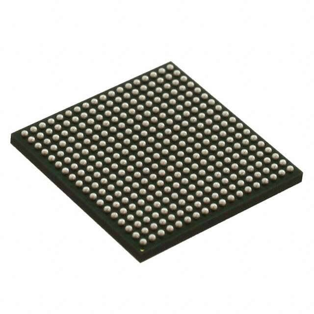


 工商网监
湘ICP备2023018690号
工商网监
湘ICP备2023018690号
