������
���
�
�
�������� ������ ��������� �
���� �����
��� �������
�
SLUS468E− MAY 2001 − REVISED APRIL 2002
D Provides Accurate Measurement of
D
D
D
D
D
D
D
D
D
Available Charge in Li-Ion Batteries
Supports the 2-Wire SMBus V1.1 Interface
With PEC or Single-Wire HDQ16
Directly Interfaces the Seiko S-8243
Protection IC for Maximum Safety
Protection and Minimal Component Count
Supports Internal or External Thermistor
Reports Individual Cell Voltages
Uses 15-Bit ADC for Accurate Voltage,
Temperature, and Current Measurements
Measures Charge Flow Using A V-to-F
Converter With Offset of Less Than 16 µV
After Calibration
Consumes Less Than 0.5 mW Operating
Drives 4- or 5-Segment LED Display for
Remaining Capacity Indication
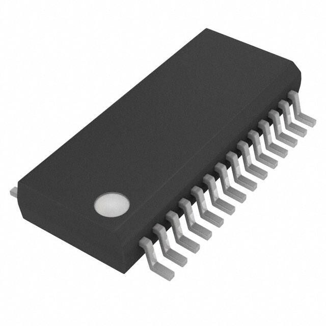
28-Pin 150-Mil SSOP
SSOP (DBQ) PACKAGE
(TOP VIEW)
HDQ16
ESCL
ESDA
RBI
REG
VOUT
VCC
VSS
CTL2
CTL3
CTL4
LED1
LED2
LED3
1
2
3
4
5
6
7
8
9
10
11
12
13
14
28
27
26
25
24
23
22
21
20
19
18
17
16
15
SMBC
SMBD
SAFETY
GND
GND
VCELL
SR1
SR2
SRC
TS
THON
DISP
LED5
LED4
description
The bq2063 SBS-compliant gas gauge IC for battery-pack or in-system installation maintains an accurate
record of available charge in Li-Ion batteries. The bq2063 monitors capacity and other critical parameters in
Li-Ion battery packs. It also directly interfaces the Seiko S-8243 protection IC to minimize component count in
smart-battery circuits.
The bq2063 uses a V-to-F converter with automatic offset correction for charge and discharge counting. For
voltage, temperature, and current reporting, the bq2063 uses an A-to-D converter. In conjunction with the
S-8243, the onboard ADC also monitors individual cell voltages in a Li-Ion battery pack and allows the bq2063
to generate control signals to enhance pack safety.
The bq2063 supports the smart battery data (SBData) commands and charge-control functions. It
communicates data using the system management bus (SMBus) 2-wire protocol or the 1-wire HDQ16 protocol.
The data available include the battery’s remaining capacity, temperature, voltage, current, and remaining
run-time predictions. The bq2063 provides LED drivers and a push-button input to depict remaining battery
capacity from full to empty in 20% or 25% increments with a 4- or 5-segment display.
The bq2063 works with an external EEPROM. The EEPROM stores the configuration information for the
bq2063, such as the battery’s chemistry, self-discharge rate, rate-compensation factors, measurement
calibration, and design voltage and capacity. The bq2063 uses the programmable self-discharge rate and other
compensation factors stored in the EEPROM to accurately adjust remaining capacity for use and standby
conditions based on time, rate, and temperature. The bq2063 also automatically calibrates or learns the true
battery capacity in the course of a discharge cycle from programmable near full to near empty levels.
The S-8243 protection IC may be used to provide power to the bq2063 from a 3- or 4-series Li-Ion cell stack.
AVAILABLE OPTIONS
PACKAGE
TJ
28-LEAD SSOP
(DBQ)
−20°C to 70°C
bq2063DBQ
Please be aware that an important notice concerning availability, standard warranty, and use in critical applications of
Texas Instruments semiconductor products and disclaimers thereto appears at the end of this data sheet.
Copyright 2002, Texas Instruments Incorporated
�����
���� ���� ��!"#$%&�"� �' ()##*�& %' "! +)�,�(%&�"� -%&*�
�#"-)(&' ("�!"#$ &" '+*(�!�(%&�"�' +*# &.* &*#$' "! �*/%' ��'&#)$*�&'
'&%�-%#- 0%##%�&1� �#"-)(&�"� +#"(*''��2 -"*' �"& �*(*''%#�,1 ��(,)-*
&*'&��2 "! %,, +%#%$*&*#'�
POST OFFICE BOX 655303
• DALLAS, TEXAS 75265
1
�������
���
�
�
�������� ������ ��������� �
���� �����
��� �������
�
SLUS468E− MAY 2001 − REVISED APRIL 2002
Terminal Functions
TERMINAL
NAME
CTL2−CTL4
No.
9–11
I/O
DESCRIPTION
O
3-state outputs to interface the S-8243 protection IC
DISP
17
I
Display control for the LED drivers LED1−LED5
ESCL
2
O
Serial memory clock for data transfer between the bq2063 and the external nonvolatile configuration memory
ESDA
3
I/O
Bidirectional pin that transfers address and data to and from the bq2063 and the external nonvolatile
configuration memory
GND
24–25
HDQ16
Must be tied externally to VSS
1
I/O
Serial communication open-drain bidirectional communications port
12–16
O
LED display segments that each may drive an external LED
4
I
Register backup that provides backup potential to the bq2063 registers during periods of low operating
voltage. RBI accepts a storage capacitor or a battery input
REG
5
O
Regular output to control an n-JFET for Vcc regulation to the bq2063 from the battery potential
SAFETY
26
O
Open-drain output for an additional level of safety protection (e.g., fuse blow)
SMBC
28
I/O
SMBus clock open-drain bidirectional pin used to clock the data transfer to and from the bq2063
SMBD
27
I/O
SMBus data open-drain bidirectional pin used to transfer address and data to and from the bq2063
SRC
20
I
Current-sense voltage to monitor instantaneous current
LED1−LED5
RBI
SR1−SR2
22–21
I
Connections for a small-value sense resistor to monitor the battery charge- and discharge-current flow
THON
18
O
Control for external FETs to connect the thermistor bias resistor during a temperature measurement
TS
19
I
Thermistor voltage input connection to monitor temperature
VCC
7
I
Supply voltage
VCELL
23
I
Single-cell voltage input that monitors the series element cell voltages from the S-8243
VOUT
6
O
VSS
8
VCC output that supplies power to the external EEPROM configuration memory
Ground
absolute maximum ratings over operating free-air temperature (unless otherwise noted)†
Supply voltage (VCC with respect to VSS) . . . . . . . . . . . . . . . . . . . . . . . . . . . . . . . . . . . . . . . . . . . . . . . . . . . . . . 6 V
Input voltage, V(IN), all other pins (all with respect to VSS) . . . . . . . . . . . . . . . . . . . . . . . . . . . . . . . . . . . . . . . . 6 V
Operating free-air temperature range, TA . . . . . . . . . . . . . . . . . . . . . . . . . . . . . . . . . . . . . . . . . . . . −20°C to 70°C
Storage temperature range, TSTG . . . . . . . . . . . . . . . . . . . . . . . . . . . . . . . . . . . . . . . . . . . . . . . . . . . −20°C to 70°C
Junction temperature range, TJ . . . . . . . . . . . . . . . . . . . . . . . . . . . . . . . . . . . . . . . . . . . . . . . . . . . . −40°C to 125°C
Lead temperature (soldering, 10 s) . . . . . . . . . . . . . . . . . . . . . . . . . . . . . . . . . . . . . . . . . . . . . . . . . . . . . . . . . 300°C
† Stresses beyond those listed under “absolute maximum ratings” may cause permanent damage to the device. These are stress ratings only, and
functional operation of the device at these or any other conditions beyond those indicated under “recommended operating conditions” is not
implied. Exposure to absolute-maximum-rated conditions for extended periods may affect device reliability.
2
POST OFFICE BOX 655303
• DALLAS, TEXAS 75265
�������
���
�
�
�������� ������ ��������� �
���� �����
��� �������
�
SLUS468E− MAY 2001 − REVISED APRIL 2002
electrical characteristics for VCC = 2.7 V to 3.7 V, TA = −20°C to 70°C (unless otherwise noted)
PARAMETER
TEST CONDITIONS
VCC
ICC
Supply voltage
Operating current
VOUT inactive
I(SLP)
I(LVOUT)
Low-power storage mode current
1.5 V < VCC < 3.7 V
VOUT leakage current
VOUT inactive
I(VOUT)
VOUT source current
VOUT active,
VOUT = VCC − 0.6 V
VI(OLS)
V(IL)
Output voltage low: (LED1−LED5, CTL2−4)
I(OLS) = 5 mA
VIH
Input voltage high DISP
VOL
Output voltage low SMBC, SMBD, HDQ16, ESCL,
ESDA, THON
MIN
TYP
2.7
Input voltage low SMBC, SMBD, HDQ16, ESCL, ESDA
V(AI)
I(RB)
Input voltage range VCELL, TS, SRC
V(RBI)
Z(AI1)
RBI data-retention voltage
Input impedance SR1, SR2
Z(AI2)
Input impedance VCELL, TS, SRC
3.3
3.7
V
235
µA
5
10
µA
0.2
µA
−5
mA
0.4
V
−0.3
0.8
V
2
VCC + 0.3
V
0.4
V
0.8
V
1.7
6
V
VSS − 0.3
1.25
V
50
nA
IOL = 1 mA
−0.3
Input voltage high SMBC, SMBD, HDQ16, ESCL, ESDA
V(RBI) > 3 V, VCC < 2 V
RBI data-retention input current
UNIT
180
−0.2
Input voltage low DISP
V(ILS)
V(IHS)
MAX
10
1.3
V
0 V–1.25 V
10
MΩ
0 V–1.25 V
5
MΩ
VFC characteristics, VCC = 3.1 V to 3.5 V, TA= 0°C to 70°C (unless otherwise noted)
PARAMETER
TEST CONDITIONS
V(SR)
V(SROS)
Input voltage range, V(SR2) and V(SR1)
V(SRCOS)
RMVCO
Calibrated offset
RM(TCO)
INL
Input offset
VSR = V(SR2) – V(SR1)
V(SR2) = V(SR1), autocorrection disabled
MIN
TYP
–0.25
–250
–50
MAX
UNIT
0.25
V
250
µV
16
µV
1.2
%/V
%/°C
–16
Supply voltage gain coefficient
VCC = 3.5 V
Slope for TA = –20°C to 70°C
Temperature gain coefficient (see Note 1)
0.8
–0.09
0.09
Total Deviation TA = –20°C to 70°C
–1.6%
0.1%
Slope for TA = −0°C to 50°C
Total Deviation TA = −0°C to 50°C
–0.05
0.05
–0.6%
0.1%
Integral nonlinearity error
TA = 0°C to 50°C
NOTE 1: RM(TCO) total deviation is from the nominal VFC gain at 25°C.
%/°C
0.21%
REG characteristics (see Note 2)
PARAMETER
V(RO)
REG controlled output voltage
TEST CONDITIONS
MIN
TYP
MAX
JFET: R(ds)(on) < 150 Ω
V(gs)(off) ≤ −3 V at 10 µA
3.1
3.3
3.5
IREG
REG(output current)
1
NOTE 2: Characteristics for internal bq2063 regulator control. Leave REG pin open when using regulated voltage from S-8243.
POST OFFICE BOX 655303
• DALLAS, TEXAS 75265
UNIT
V
µA
3
�������
���
�
�
�������� ������ ��������� �
���� �����
��� �������
�
SLUS468E− MAY 2001 − REVISED APRIL 2002
SMBus ac specifications, TA = −20°C to 70°C, 2.7 V < VCC < 3.7 V (unless other noted)
PARAMETER
TEST CONDITIONS
MIN
TYP
UNIT
100
kHz
FSMB
FMAS
SMBus operating frequency
Slave mode, SMBC 50% duty cycle
SMBus master clock frequency
Master mode, no clock low slave extend
TBUF
THD:STA
Bus free time between start and stop
4.7
µs
Hold time after (repeated) start
4.0
µs
TSU:STA
TSU:STO
Repeated start setup time
4.7
µs
4.0
µs
Stop setup time
10
MAX
51.2
Receive mode
0
Transmit mode
300
kHz
µss
THD:DAT
Data hold time
TSU:DAT
TTIMEOUT
Data setup time
TLOW
THIGH
Clock low period
Clock high period
See Note 4
50
µs
TLOW:SEXT
TLOW:MEXT
Cumulative clock low slave extend time
See Note 5
25
ms
Cumulative clock low master extend time
See Note 6
10
ms
µs
250
Error signal/detect
See Note 3
25
35
ms
µs
4.7
4.0
NOTES: 3. The bq2063 times out when any clock low exceeds TTIMEOUT
4. THIGH Max. is minimum bus idle time. SMBC = SMBD = 1 for t > 50 µs causes reset of any transaction involving bq2063 that is in
progress.
5. TLOW:SEXT is the cumulative time a slave device is allowed to extend the clock cycles in one message from initial start to the stop.
6. TLOW:MEXT is the cumulative time a master device is allowed to extend the clock cycles in one message from initial start to the stop.
HDQ16 ac specifications, TA = −20°C to 70°C, 2.7 V < VCC < 3.7 V (unless otherwise noted)
PARAMETER
TEST CONDITIONS
MIN
TYP
MAX
UNIT
µs
tCYCH
tCYCB
Cycle time, host to bq2063 (write)
190
Cycle time, bq2063 to host (read)
190
tSTRH
tSTRB
Start hold time, host to bq2063 (write)
5
Start hold time, bq2063 to host (read)
32
tDSU
tDSUB
Data setup time
t(DH)
tDV
Data hold time
100
µs
Data valid time
80
µs
tSSU
tSSUB
Stop setup time
145
µs
Stop setup time
145
µs
tRSPS
tB
Response time, bq2063 to host
190
320
µs
Break time
190
µs
tBR
Break recovery time
40
µs
4
Data setup time
POST OFFICE BOX 655303
• DALLAS, TEXAS 75265
205
250
µs
µs
µs
50
µs
50
µs
�������
���
�
�
�������� ������ ��������� �
���� �����
��� �������
�
SLUS468E− MAY 2001 − REVISED APRIL 2002
Figures 1−4 illustrate the diagrams for the bq2063.
THIGH
SMBC
THD:STA
TLOW
THD:DAT
TSU:STA
TSU:STO
TSU:DAT
SMBD
TBUF
Figure 1. SMBus Timing Data
tBR
tB
Figure 2. HDQ16 Break Timing
Write 1
Write 0
tSTRH
tDSU
tDH
tSSU
tCYCH
Figure 3. HDQ16 Host to bq2063
Read 1
Read 0
tSTRB
tDSUB
tDV
tSSUB
tCYCB
Figure 4. HDQ16 bq2063 to Host
POST OFFICE BOX 655303
• DALLAS, TEXAS 75265
5
�������
���
�
�
�������� ������ ��������� �
���� �����
��� �������
�
SLUS468E− MAY 2001 − REVISED APRIL 2002
functional description
general operation
The bq2063 determines battery capacity by monitoring the amount of charge input or removed from a
rechargeable battery. In addition to measuring charge and discharge, the bq2063 measures battery voltage,
temperature, and current, estimates battery self-discharge, and monitors the battery for low-voltage thresholds.
The bq2063 measures charge and discharge activity by monitoring the voltage across a small-value series
sense resistor between the battery’s negative terminal and the negative terminal of the battery pack. The
available battery charge is determined by monitoring this voltage and correcting the measurement for
environmental and operating conditions.
The bq2063 accepts an NTC thermistor (Semitec 103AT) for temperature measurement or can be configured
for internal IC measurement. The bq2063 uses temperature to monitor battery pack and to compensate the
self-discharge estimate.
measurements
The bq2063 uses a fully differential, dynamically balanced voltage-to-frequency converter (VFC) for charge
measurement and a sigma delta analog-to-digital converter (ADC) for battery voltage, current, and temperature
measurement.
Voltage, current, and temperature measurements are made every 2−2.2 seconds, depending on the bq2063
operating mode. Maximum times occur with compensated EDV, mWh mode, and maximum allowable
discharge rate. Any AtRate computations requested or scheduled (every 20 seconds) may add up to 0.5
seconds to the time interval.
charge and discharge counting
The VFC measures the charge and discharge flow of the battery by monitoring a small-value sense resistor
between the SR1 and SR2 pins as shown in Figure 13. The VFC measures bipolar signals up to 250 mV. The
bq2063 detects charge activity when VSR = V(SR2)–V(SR1) is positive and discharge activity when
VSR = V(SR2)–V(SR1) is negative. The bq2063 continuously integrates the signal over time using an internal
counter. The fundamental rate of the counter is 6.25 µVh.
offset calibration
The bq2063 provides an auto-calibration feature to cancel the voltage offset error across SR1 and SR2 for
maximum charge measurement accuracy. The calibration routine is initiated by issuing a command to
ManufacturerAccess( ). The bq2063 is capable of automatic offset calibration down to 6.25µV. Offset
cancellation resolution is less than 1 µV.
digital filter
The bq2063 does not measure charge or discharge counts below the digital filter threshold. The digital filter
threshold is programmed in the EEPROM and should be set sufficiently high to prevent false signal detection
with no charge or discharge flowing through the sense resistor.
voltage
While monitoring SR1 and SR2 for charge and discharge currents, the bq2063 monitors the battery-pack
potential and the individual cell voltages through the VCELL pin. The bq2063 measures the voltage of three or
four series elements in a battery pack. CTL3 and CTL4 signal the S-8243 to present the cell voltages at the
VCELL input of the bq2063 according to Table 11. The bq2063 calculates the pack voltage and reports the result
in Voltage( ). The individual cell voltages are stored in the optional manufacturer function area.
6
POST OFFICE BOX 655303
• DALLAS, TEXAS 75265
�������
���
�
�
�������� ������ ��������� �
���� �����
��� �������
�
SLUS468E− MAY 2001 − REVISED APRIL 2002
functional description (continued)
current
The SRC input of the bq2063 measures battery charge and discharge current. The SRC ADC input converts
the current signal from the series sense resistor and stores the result in Current( ). The full-scale input range
to SBC is limited to ±250 mV.
temperature
The bq2063 can use its internal sensor or an external thermistor to develop the temperature reading, depending
on the programming of the EXTH bit in Pack Configuration, EE 0x3f.
The TS input of the bq2063 in conjunction with an NTC thermistor measures the battery temperature as shown
in Figure 13. The bq2063 reports temperature in Temperature( ). THON may be used to switch the bias current
through the external thermistor when the bq2063 samples the TS input. THON is low impedance for 60 ms when
the temperature is measured, and high impedance otherwise.
gas gauge operation
general
The operational overview in Figure 5 illustrates the gas gauge operation of the bq2063. Table 2 describes the
bq2063 registers.
Inputs
Charge
Current
Battery Load and Light
Discharge Estimate
Discharge
Current
Charge
Efficiency
Compensation
Temperature
Compensation
−
Main Counters and
Capacity Reference (FCC)
Self-Discharge
Timer
+
−
−
Remaining
Capacity
(RM)
+
≤
Full
Charge
Capacity
(FCC)
+
+
Discharge
Count
Qualified Register
(DCR)
Transfer
Temperature, Other Data
Outputs
Chip-Controlled
Available Charge
LED Display
Two-Wire
Serial Port
Figure 5. bq2063 Operational Overview
POST OFFICE BOX 655303
• DALLAS, TEXAS 75265
7
�������
���
�
�
�������� ������ ��������� �
���� �����
��� �������
�
SLUS468E− MAY 2001 − REVISED APRIL 2002
general (continued)
The bq2063 accumulates a measure of charge and discharge currents and estimates self-discharge of the
battery. The bq2063 compensates the charge current measurement for temperature and state-of-charge of the
battery. The bq2063 also adjusts the self-discharge estimation based on temperature.
The main charge counter RemainingCapacity( ) (RM) represents the available capacity or energy in the battery
at any given time. The bq2063 adjusts RM for charge, self-discharge, and leakage compensation factors. The
information in the RM register is accessible through the communications ports and is also represented through
the LED display.
The FullChargeCapacity( ) (FCC) register represents the last measured full discharge of the battery. It is used
as the battery’s full-charge reference for relative capacity indication. The bq2063 updates FCC after the battery
undergoes a qualified discharge from nearly full to a low battery level. FCC is accessible through the serial
communications ports.
The Discharge Count Register (DCR) is a non-accessible register that tracks discharge of the battery. The
bq2063 uses the DCR register to update the FCC register if the battery undergoes a qualified discharge from
nearly full to a low battery level. In this way, the bq2063 learns the true discharge capacity of the battery under
system use conditions.
main gas-gauge registers
The gas-gauge register functions are described in Table 2.
RemainingCapacity( ) (RM)
RM represents the remaining capacity in the battery. The bq2063 computes RM in either mAh or 10 mWh
depending on the selected mode.
RM counts up during charge to a maximum value of FCC and down during discharge and self-discharge to 0.
In addition to charge and self-discharge compensation, the bq2063 calibrates RM at three low-battery-voltage
thresholds, EDV2, EDV1, and EDV0 and three programmable midrange thresholds VOC25, VOC50, and
VOC75. This provides a voltage-based calibration to the RM counter.
DesignCapacity( ) (DC)
The DC is the user-specified battery full capacity. It is calculated from Pack Capacity EE 0x3a-0x3b and is
represented in mAh or 10 mWh. It also represents the full-battery reference for the absolute display mode.
FullChargeCapacity( ) (FCC)
FCC is the last measured discharge capacity of the battery. It is represented in either mAh or 10 mWh,
depending on the selected mode. On initialization, the bq2063 sets FCC to the value stored in Last Measured
Discharge EE 0x38-0x39. During subsequent discharges, the bq2063 updates FCC with the last measured
discharge capacity of the battery. The last measured discharge of the battery is based on the value in the DCR
register after a qualified discharge occurs. Once updated, the bq2063 writes the new FCC value to EEPROM
in mAh to Last Measured Discharge. FCC represents the full battery reference for the relative display mode and
relative state of charge calculations.
discharge count register (DCR)
The DCR register counts up during discharge, independent of RM. DCR can continue to count even after RM
has counted down to 0. Before RM = 0, discharge activity, light discharge estimation, battery load estimation,
and self-discharge increment DCR. After RM = 0, the bq2063 does not apply self-discharge and DCR
increments only because of discharge activity, light discharge estimation, and battery load estimation. The
bq2063 initializes DCR, at the beginning of a discharge, to FCC − RM when RM is within twice the programmed
value in Near Full EE 0x55. The DCR initial value of FCC − RM is reduced by FCC/128 if SC = 0 (bit 2 in Control
Mode) and is not reduced if SC = 1. DCR stops counting when the battery voltage reaches the EDV2 threshold
on discharge.
8
POST OFFICE BOX 655303
• DALLAS, TEXAS 75265
�������
���
�
�
�������� ������ ��������� �
���� �����
��� �������
�
SLUS468E− MAY 2001 − REVISED APRIL 2002
gas gauge operation (continued)
capacity learning (FCC update) and qualified discharge
The bq2063 updates FCC with an amount based on the value in DCR if a qualified discharge occurs. The new
value for FCC equals the DCR value plus the programmable nearly full and low battery levels, according to the
following equation:
FCC (new) + DCR (final) + DCR (initial) ) Measured Discharge to EDV2 ) (FCC
Battery Low%)
(1)
Battery Low % = (value stored in EE 0x54) ÷ 2.56
A qualified discharge occurs if the battery discharges from RM ≥ FCC − Near Full × 2 to the EDV2 voltage
threshold with the following conditions:
D No valid charge activity occurs during the discharge period. A valid charge is defined as a charge of 10 mAh
into the battery.
D No more than 256 mAh of self-discharge, battery load estimation, and/or light discharge estimation occurs
during the discharge period.
D The temperature does not drop below the low temperature thresholds programmed in Max T_LowT or 12°C
during the discharge period. The threshold depends on the programming of the LLTF bit in Pack
Programming, EE 0x63.
D The battery voltage reaches the EDV2 threshold during the discharge period and the voltage was less than
the EDV2 threshold minus 256 mV when the bq2063 detected EDV2.
D No midrange voltage correction occurs during the discharge period.
D Current remains ≥ 3C/32 or C/32, depending on Pack Programming selection, when EDV2 or Battery Low
% level is reached.
The bq2063 sets VDQ=1 in Pack Status when qualified discharge begins. The bq2063 sets VDQ=0 if any
disqualifying condition occurs. FCC cannot be reduced by more than 256 mAh or increased by more than
512 mAh during any single update cycle. The bq2063 saves the new FCC value to the EEPROM within 4
seconds of being updated.
end-of-discharge thresholds and capacity correction
The bq2063 monitors the battery for three low-voltage thresholds, EDV0, EDV1, and EDV2. The EDV
thresholds can be programmed for determination based on the overall pack voltage or an individual cell level.
The EDVV bit in Pack Programming configures the bq2063 for overall voltage or single-cell EDV thresholds.
If programmed for single cell EDV determination, the bq2063 determines EDV on the basis of the lowest
single-cell voltage. Fixed EDV thresholds may be programmed in EDVF/EDV0 EE 0x72-0x73, EMF/EDV1 EE
0x74-0x75, and EDV C0 Factor/EDV2 EE 0x78-0x79. If the CEDV bit in Pack Configuration is set, automatic
EDV compensation is enabled and the bq2063 computes the EDV0, EDV1, and EDV2 thresholds based on the
values in EE 0x72-0x7d, 0x06, and the battery’s current discharge rate and temperature. The bq2063 disables
EDV detection if Current( ) exceeds the Overload Current threshold programmed in EE 0x46 − EE 0x47. The
bq2063 resumes EDV threshold detection after Current( ) drops below the overload current threshold. Any EDV
threshold detected is reset after 10 mAh of charge are applied.
POST OFFICE BOX 655303
• DALLAS, TEXAS 75265
9
�������
���
�
�
�������� ������ ��������� �
���� �����
��� �������
�
SLUS468E− MAY 2001 − REVISED APRIL 2002
end-of-discharge thresholds and capacity correction (continued)
Table 1. State of Charge Based on Low Battery Voltage
THRESHOLD
RELATIVE STATE
OF CHARGE
EDV0
0%
EDV1
3%
EDV2
Battery Low %
The bq2063 uses the EDV thresholds to apply voltage-based corrections to the RM register according to
Table 1. The bq2063 performs EDV-based RM adjustments with Current( ) ≥ C/32. No EDVs are set if current
< C/32. The bq2063 adjusts RM as it detects each threshold. If the voltage threshold is reached before the
corresponding capacity on discharge, the bq2063 reduces RM to the appropriate amount as shown in Table 1.
This reduction occurs only if current ≥ C/32 when the EDV threshold is detected. If RM reaches the capacity
level before the voltage threshold is reached on discharge, the bq2063 prevents RM from decreasing further
until the battery voltage reaches the corresponding threshold only on a full learning cycle discharge. RM is not
held at the associated EDV percentage on a nonlearning discharge cycle (VDQ=0) or if current < C/32.
Table 2. bq2063 Register Functions
COMMAND CODE
FUNCTION
10
SMBus
HDQ16
ACCESS
(SMBus)
UNITS
ManufacturerAccess
0x00
0x00
read/write
NA
RemainingCapacityAlarm
0x01
0x01
read/write
mAh, 10 mWh
RemainingTimeAlarm
0x02
0x02
read/write
minutes
BatteryMode
0x03
0x03
read/write
NA
AtRate
0x04
0x04
read/write
mA, 10mW
AtRateTimeToFull
0x05
0x05
read
minutes
AtRateTimeToEmpty
0x06
0x06
read
minutes
AtRateOK
0x07
0x07
read
Boolean
Temperature
0x08
0x08
read
0.1°K
Voltage
0x09
0x09
read
mV
Current
0x0a
0x0a
read
mA
AverageCurrent
0x0b
0x0b
read
mA
MaxError
0x0c
0x0c
read
percent
RelativeStateOfCharge
0x0d
0x0d
read
percent
AbsoluteStateOfCharge
0x0e
0x0e
read
percent
RemainingCapacity
0x0f
0x0f
read
mAh, 10 mWh
FullChargeCapacity
0x10
0x10
read
mAh, 10 mWh
RunTimeToEmpty
0x11
0x11
read
minutes
AverageTimeToEmpty
0x12
0x12
read
minutes
AverageTimeToFull
0x13
0x13
read
minutes
ChargingCurrent
0x14
0x14
read
mA
ChargingVoltage
0x15
0x15
read
mV
Battery Status
0x16
0x16
read
NA
CycleCount
0x17
0x17
read
cycles
DesignCapacity
0x18
0x18
read
mAh, 10 mWh
DesignVoltage
0x19
0x19
read
mV
SpecificationInfo
0x1a
0x1a
read
NA
ManufactureDate
0x1b
0x1b
read
NA
POST OFFICE BOX 655303
• DALLAS, TEXAS 75265
�������
���
�
�
�������� ������ ��������� �
���� �����
��� �������
�
SLUS468E− MAY 2001 − REVISED APRIL 2002
Table 2. bq2063 Register Functions (Continued)
FUNCTION
COMMAND CODE
SMBus
ACCESS
(SMBus)
HDQ16
UNITS
SerialNumber
0x1c
0x1c
read
integer
Reserved
0x1d-0x1f
0x1d−0x1f
—
—
ManufacturerName
0x20
0x20−0x25
read
string
DeviceName
0x21
0x28−0x2b
read
string
DeviceChemistry
0x22
0x30−0x32
read
string
ManufacturerData
0x23
0x38−0x3b
read
string
Pack Status
0x2f (LSB)
0x2f (LSB)
read/write
NA
Pack Configuration
0x2f (MSB)
0x2f (MSB)
read/write
NA
VCELL4
0x3c
0x3c
read/write
mV
VCELL3
0x3d
0x3d
read/write
mV
VCELL2
0x3e
0x3e
read/write
mV
VCELL1
0x3f
0x3f
read/write
mV
self-discharge
The bq2063 estimates the self-discharge of the battery to maintain an accurate measure of the battery capacity
during periods of inactivity. The algorithm for self-discharge estimation takes a programmed estimate for the
expected self-discharge rate at 25°C stored in EEPROM and makes a fixed reduction to RM of an amount equal
to RemainingCapacity( )/256. The bq2063 makes the fixed reduction at a varying time interval that is adjusted
to achieve the desired self-discharge rate. This method maintains a constant granularity of 0.39% for each
self-discharge adjustment, which may be performed multiple times per day, instead of once per day with a
potentially large reduction.
The self-discharge estimation rate for 25°C is doubled for each 10 degrees above 25°C or halved for each 10
degrees below 25°C. The following table shows the relation of the self-discharge estimation at a given
temperature to the rate programmed for 25°C (Y% per day).
Table 3. Self-Discharge for Rate Programmed
TEMPERATURE
(°C)
SELF-DISCHARGE RATE
Temp < 10
1/4 Y% per day
10 ≤ Temp EDV2 threshold (discharging)
Voltage ≤ EDV2 threshold
EINT
The EINT bit indicates that the VFC has detected a charge or discharge pulse.
0
1
No charge/discharge activity detected
Charge/discharge activity detected
VDQ
The VDQ bit indicates if the present discharge cycle is valid for an FCC update.
0
1
40
Discharge cycle not valid
Discharge cycle valid
POST OFFICE BOX 655303
• DALLAS, TEXAS 75265
�������
���
�
�
�������� ������ ��������� �
���� �����
��� �������
�
SLUS468E− MAY 2001 − REVISED APRIL 2002
SOV
The SOV bit indicates that the safety output limits have been exceeded. Once set, the FLAG stays set until the
bq2063 is reset.
0
1
Safety limits not exceeded
Safety limits exceeded
CVOV
The CVOV bit indicates that a secondary Li-Ion protection limit has been exceeded. It is set on a prolonged
overcurrent, overvoltage, or overtemperature condition. The bit is not latched and merely reflects the present
overvoltage status.
0
1
No secondary protection limits exceeded
A secondary protection limit exceeded
CVUV
The CVUV bit indicates that a secondary Li-Ion protection limit has been exceeded. It is set on an overload or
over-discharge condition. The bit is not latched and merely reflects the present undervoltage status.
0
1
No secondary protection limits exceeded
A secondary protection limit exceeded
VCELL4-VCELL1 (0x3c-0x3f); [0x3c-0x3f]
These functions return the calculated individual cell voltages in mV.
EEPROM
general
The bq2063 accesses the external EEPROM during reset and when storing historical data. During an EEPROM
access, the VOUT pin becomes active and the bq2063 uses the ESCL and ESDA pins to communicate with
the EEPROM. The EEPROM stores basic configuration information for use by the bq2063. The EEPROM must
be programmed correctly for proper bq2063 operation.
memory map
Table 12 shows the memory map for the EEPROM. It contains example data for a 3s3p Li-Ion battery pack with
a 0.05-Ω sense resistor.
Table 10. EEPROM Memory Map
DATA
EEPROM ADDRESS
NAME
Li-ION EXAMPLE
MSB
LSB
0x00
0x01
Check Byte 1
15487
3c
7f
0x02
0x03
Remaining Time Alarm
10 minutes
00
0a
0x04
0x05
Remaining Capacity Alarm
400 mAh
01
90
0x06
EDV C1 Factor
0
00
0x07
EDV TC Factor
0
00
0x08
Safety Overtemperature
75°C
c3
0x09
Reserved
0
00
Charging Voltage
12600 mV
0x0a
0x0b
31
38
NOTE: Reserved locations must be set as shown. Locations marked with an * are calibration values that can be
adjusted for maximum accuracy. For these locations the table shows the appropriate default or initial setting.
POST OFFICE BOX 655303
• DALLAS, TEXAS 75265
41
�������
���
�
�
�������� ������ ��������� �
���� �����
��� �������
�
SLUS468E− MAY 2001 − REVISED APRIL 2002
Table 10. EEPROM Memory Map (Continued)
DATA
EEPROM ADDRESS
NAME
Li-ION EXAMPLE
MSB
LSB
0x0c
0x0d
Reserved
128
00
80
0x0e
0x0f
Cycle Count
0
00
00
0x10
0x11
Reserved
0
00
00
0x12
0x13
Design Voltage
10800 mV
2a
30
0x14
0x15
Specification Information
v1.1/PEC
00
31
0x16
0x17
Manufacture Date
2/25/99=9817
26
59
0x18
0x19
Serial Number
1
00
01
0x1a
0x1b
Fast-Charging Current
3000 mA
0b
b8
0x1c
Pack Load Estimate
0 mA
0x1d
Maintenance Charging Current
0 mA
00
00
0x1e
Pre-Charge Current
96 mA
00
0C
0x1f
Safety Overvoltage
13056 mV
8C
0x20
Manufacturer Name Length
9
09
0x21
Character 1
B
42
0x22
Character 2
E
45
0x23
Character 3
N
4e
0x24
Character 4
C
43
0x25
Character 5
H
48
0x26
Character 6
M
4d
0x27
Character 7
A
41
0x28
Character 8
R
52
0x29
Character 9
Q
51
0x2a
Character 10
—
00
0x2b
Character 11
—
00
00
0x2c
0x2d
Reserved
0
00
00
0x2e
0x2f
Maximum Overcharge
350 mAh
fe
a2
0x30
Device Name Length
6
06
0x31
Character 1
B
42
0x32
Character 2
Q
51
0x33
Character 3
2
32
0x34
Character 4
0
30
0x35
Character 5
6
36
0x36
Character 6
3
33
0x37
Character 7
—
00
0x38
0x39
Last Measured Discharge
4500 mAh
11
94
0x3a
0x3b
Pack Capacity
0x3c
0x3d
Cycle Count Threshold
4500 mAh
11
94
3600 mAh
0e
10
0x3e
Reserved
0
00
0x3f
Pack Configuration
DMODE, SEAL,
CSYNC, OTVC
e2
0x40
Device Chemistry Length
4
04
0x41
Character 1
L
4c
NOTE: Reserved locations must be set as shown. Locations marked with an * are calibration values that can be
adjusted for maximum accuracy. For these locations the table shows the appropriate default or initial setting.
42
POST OFFICE BOX 655303
• DALLAS, TEXAS 75265
�������
���
�
�
�������� ������ ��������� �
���� �����
��� �������
�
SLUS468E− MAY 2001 − REVISED APRIL 2002
Table 10. EEPROM Memory Map (Continued)
EEPROM ADDRESS
NAME
Li-ION EXAMPLE
DATA
MSB
LSB
0x42
Character 2
I
0x43
Character 3
O
4f
0x44
Character 4
N
4e
0x45
MaxT LowT
50°C, 4.8°C
c6
0x46
0x47
49
Overload Current
6000 mA
0x48
Overvoltage Margin
800 mV
17
70
32
0x49
Overcurrent Margin
512 mA
20
0x4a
Cell Under/Over Voltage
2496 mV/4384 mV
79
0x4b
Fast Charge Termination %
100%
ff
a1
0x4c
Fully Charged Clear %
95%
0x4d
Charge Efficiency
100%
ff
0x4e
Current Taper Threshold
200 mA
08
0x4f
Current Taper Qual Voltage
128 mV
40
0x50
Manufacturer Data Length
7
07
0x51
Control Mode
SC
04
0x52
Digital Filter
50 µV
2d
0x53
Self-Discharge Rate
0.21%
05
0x54
Battery Low %
7%
12
0x55
Near Full
200 mAh
64
0x56
0x57
Reserved
0
00
00
0x58
0x59
Reserved
0
00
00
0x5a
0x5b
Reserved
0
00
00
0x5c
0x5d
Reserved
0
00
00
0x5e
0x5f
VFC Offset*
0
00
00
0x60
VFC Offset*
0
-
00
0x61
Temperature Offset*
0
-
00
0x62
ADC Offset*
0
-
00
0x63
Pack Programming
PDLY
-
01
0x64
Light Load Estimate
0
-
00
0x65
Reserved
0
-
00
0x66
0x67
ADC Voltage Gain*
5:1
30
d4
0x68
0x69
ADC Sense Resistor Gain*
0.05 Ω
30
d4
0x6a
0x6b
VFC Sense Resistor Gain*
0.05 Ω
20
00
0x6c
0x6d
VOC25
11170 mV
d4
5e
0x6e
0x6f
VOC50
11370 mV
d3
96
0x70
0x71
VOC75
11730 mV
d2
2e
0x72
0x73
EDVF/EDV0
3000 mV
0b
b8
0x74
0x75
EMF/ EDV1
3433 mV
0d
69
0x76
0x77
EDV T0 Factor
0
00
00
0x78
0x79
EDV C0 Factor/EDV2
3567 mV
0d
ef
0x7a
0x7b
EDV R0 Factor
0
00
e0
0x7c
0x7d
EDV R1 Factor
0
00
00
0x7e
0x7f
Check Byte 2
42330
a5
5a
NOTE: Reserved locations must be set as shown. Locations marked with an * are calibration values that can be
adjusted for maximum accuracy. For these locations the table shows the appropriate default or initial setting.
POST OFFICE BOX 655303
• DALLAS, TEXAS 75265
43
�������
���
�
�
�������� ������ ��������� �
���� �����
��� �������
�
SLUS468E− MAY 2001 − REVISED APRIL 2002
PROGRAMMING INFORMATION
EEPROM programming
The following sections describes the function of each EEPROM location and how the data is to be stored.
fundamental parameters
sense resistor value
Two factors are used to scale the current related measurements. The 16-bit ADC Sense Resistor Gain value
in EE 0x68-0x69 scales Current( ) to mA. Adjusting ADC Sense Resistor Gain from its nominal value provides
a method to calibrate the current readings for system errors and the sense resistor value (Rs) . The nominal
value is set by
(4)
ADC Sense Resistor Gain + 625
(Rs)
The 16-bit VFC Sense Resistor Gain in EE 0x6a-0x6b scales each VFC interrupt to mAh. VFC Sense Resistor
Gain is based on the resistance of the series sense resistor. The following formula computes a nominal or
starting value for VFC Sense Resistor Gain from the sense resistor value.
(5)
VFC Capital Sense Resistor Gain + 409.6
(Rs)
Sense resistor values are limited to the range of 0.00916 to 0.100Ω.
digital filter
The desired digital filter threshold, VDF (µV), is set by the value stored in Digital Filter EE 0x52.
(6)
Digital Filter + 2250
VDF
cell characteristics
battery pack capacity and voltage
Pack capacity in mAh units is stored in Pack Capacity, EE 0x3a-0x3b. In mAh mode, the bq2063 copies Pack
Capacity to DesignCapacity( ). In mWh mode, the bq2063 multiplies Pack Capacity by Design Voltage EE
0x12-0x13 to calculate DesignCapacity( ) scaled to 10 mWh. Design Voltage is stored in mV.
The initial value for Last Measured Discharge, in mAh, is stored in EE 0x38−0x39. Last Measured Discharge
is modified over the course of pack usage to reflect cell aging under the particular use conditions. The bq2063
updates Last Measured Discharge in mAh after a capacity learning cycle. The bq2063 uses the Last Measured
Discharge value to calculate FullChargeCapacity( ) in mAh or 10 mWh mode.
EDV thresholds and near full percentage
The bq2063 uses three pack voltage thresholds to provide voltage-based warnings of low battery capacity. The
bq2063 uses the values stored in EEPROM for the EDV0, EDV1, and EDV2 values or calculates the three
thresholds from a base value and the temperature, capacity, and rate adjustment factors stored in EEPROM.
If EDV compensation is disabled then EDV0, EDV1, and EDV2 are stored directly in mV in EE 0x72-0x73, EE
0x74-0x75, and EE 0x78-0x79, respectively.
For capacity correction at EDV2, Battery Low % EE 0x54 can be set at a desired state-of-charge,
STATEOFCHARGE%, in the range of 3-19%. Typical values for STATEOFCHARGE% are 5-7% representing
5-7% capacity.
Battery Low % = STATEOFCHARGE% • 2.56
44
POST OFFICE BOX 655303
• DALLAS, TEXAS 75265
(7)
�������
���
�
�
�������� ������ ��������� �
���� �����
��� �������
�
SLUS468E− MAY 2001 − REVISED APRIL 2002
PROGRAMMING INFORMATION
EDV thresholds and near full percentage (continued)
The bq2063 updates FCC if a qualified discharge occurs from a near-full threshold of FCC − NFW, until EDV2
condition is reached. The desired near-full threshold window, NFW (mAh), is programmed in Near Full in EE
0x55.
(8)
Near Full + NFW
2
EVD discharge rate and temperature compensation
If EDV compensation is enabled, the bq2063 calculates battery voltage to determine EDV0, EDV1, and EDV2
thresholds as a function of battery capacity, temperature, and discharge load. The general equation for EDV0,
EDV1, and EDV2 calculation is
EDV0,1,2 = EMF • FBL - | ILOAD | • R0 • FTZ
(9)
Where:
EMF is a no-load battery voltage higher than the highest EDV threshold computed. EMF is programmed in
mV in EMF/EDV1 EE 0x74-0x75.
ILOAD is the current discharge load magnitude.
FBL is the factor that adjusts the EDV voltage for battery capacity and temperature to match the no-load
characteristics of the battery.
FBL = f ( C0, C + C1, T )
(10)
Where:
C (either 0%, 3%, or Battery Low % for EDV0, EDV1, and EDV2, respectively) and C0 are the capacityrelated EDV adjustment factors. C0 is programmed in EDV C0 Factor/EDV2 EE 0x78−79. C1 is the desired
residual battery capacity remaining at EDV0 (RM = 0). The C1 factor is stored in EDV C1 Factor EE 0x06.
T is the current temperature in °K.
R0 • FTZ represents the resistance of the battery as a function of temperature and capacity.
(11)
FTZ = f ( R1 , T0, T, C + C1, TC)
R0 is the first order rate dependency factor stored in EDV R0 Factor EE 0x7a-0x7b.
T is the current temperature; C is the battery capacity relating to EDV0, EDV1, and EDV2.
R1 adjusts the variation of impedance with battery capacity. R1 is programmed in EDV R1 Rate Factor EE
0x7c-0x7d.
T0 adjusts the variation of impedance with battery temperature). T0 is programmed in EDV T0 Rate Factor EE
0x76-0x77.
TC adjusts the variation of impedance for cold temperatures (T < 23°C). TC is programmed in EDV TC EE 0x07.
POST OFFICE BOX 655303
• DALLAS, TEXAS 75265
45
�������
���
�
�
�������� ������ ��������� �
���� �����
��� �������
�
SLUS468E− MAY 2001 − REVISED APRIL 2002
PROGRAMMING INFORMATION
EVD discharge rate and temperature compensation (continued)
Typical values for the EDV compensation factors, based on overall pack voltages for a Li-lon 3s3p 18650 pack,
are
EMF = 11550
T0 = 4475
C0 = 235
C1 = 0
R0 = 5350
R1 = 250
TC = 3
The graphs in Figures 11 and 12 show the calculated EDV0, EDV1, and EDV2 thresholds versus capacity using
the typical compensation values for different temperatures and loads for a Li-Ion 3s3p 18650 pack. The
compensation values vary widely for different cell types and manufacturers and must be matched exactly to the
unique characteristics for optimal performance.
VOLTAGE
vs
CAPACITY
VOLTAGE
vs
CAPACITY
11.5
11.5
Battery Low % = 7%
Load = 500 mA
11.0
20°C
EDV2
EDV2
10.5
45°C
10.5
Battery Low % = 7%
TA = 35°C
11.0
500 mA
EDV1
V − Voltage − V
V − Voltage − V
EDV1
10.0
9.5
9.0
8.5
10.0
1A
2A
9.5
9.0
8.5
8.0
8.0
7.5
EDV0
7.5
7.0
0
1
2
3
4
5
6
7
8
9
10
0
1
Capacity − %
2
3
4
5
6
7
8
9
10
Capacity − %
Figure 11. EDV Calculations vs Capacity for
Various Temperatures
Figure 12. EDV Calculations vs Capacity for
Various Loads
overload current threshold
The Overload Current threshold is a 16-bit value stored in EE 0x46-0x47 in mA units.
midrange capacity corrections
Three voltage-based thresholds, VOC25 EE 0x6c-0x6d, VOC50 EE 0x6e-0x6f, and VOC75 EE 0x70-0x71, are
used to test the accuracy of the RM based on open-circuit pack voltages. These thresholds are stored in the
EEPROM in 2s complement of voltage in mV. The values represent the open-circuit battery voltage at which
the battery capacity should correspond to the associated state of charge for each threshold.
46
POST OFFICE BOX 655303
• DALLAS, TEXAS 75265
�������
���
�
�
�������� ������ ��������� �
���� �����
��� �������
�
SLUS468E− MAY 2001 − REVISED APRIL 2002
PROGRAMMING INFORMATION
self-discharge rate
The nominal self-discharge rate, %PERDAY (% per day), is programmed in an 8-bit value Self-Discharge Rate
EE 0x53 by the following relation:
Self-Discharge Rate + 256–
(12)
52.73
%PERDAY
light load estimate
The amount of light load current in mA, ILEAK, used for compensation is stored in Light Load Estimate in EE
0x64 as follows:
Light Discharge Current + ILEAK • 1024
45
(13)
ILEAK is between 0.044 and 11.2 mA.
charge efficiency
The bq2063 applies the efficiency factor, EFF%, to all charge added to the battery. EFF% is encoded in Charge
Efficiency EE 0x4d according to equation 16:
Charge Efficiency + (EFF% • 2.56–1)
(14)
battery electronics load
The amount of internal battery electronics load estimate in µA, BEL, is stored in Pack Load Estimate EE 0x1c
as follows;
Pack Load Estimate = 0.364 • BEL
charging voltage
The 16-bit value, Charging Voltage EE 0x0a-0x0b programs the ChargingVoltage( ) value broadcast to a Smart
Charger. It is also sets the base value for determining overvoltage conditions during charging and voltage
compliance during a constant-voltage charging methodology. It is stored in mV.
overvoltage
The 8-bit value, Overvoltage Margin EE 0x48, sets the limit over ChargingVoltage( ) that is to be considered
as an overvoltage charge-suspension condition. The voltage in mV above the ChargingVoltage( ), VOVM, that
should trigger a charge suspend is encoded in Overvoltage Margin as follows:
(15)
Overvoltage Margin + VOVM
16
VOVM is between 0 and 4080 mV.
charging current
ChargingCurrent( ) values are either broadcast to a Level 2 Smart Battery Charger or read from the bq2063 by
a Level 3 Smart Battery Charger. The bq2063 sets the value of ChargingCurrent( ), depending on the charge
requirements and charge conditions of the pack.
When fast charge is allowed, the bq2063 sets ChargingCurrent( ) to the rate programmed in Fast Charging
Current EE 0x1a-0x1b. Fast Charging Current is stored in mA.
POST OFFICE BOX 655303
• DALLAS, TEXAS 75265
47
�������
���
�
�
�������� ������ ��������� �
���� �����
��� �������
�
SLUS468E− MAY 2001 − REVISED APRIL 2002
PROGRAMMING INFORMATION
charging current (continued)
When fast charge terminates, the bq2063 sets ChargingCurrent( ) to zero and then to the Maintenance
Charging Current EE 0x1d when the termination condition ceases. MC is the desired rate in mA.
(16)
Maintenance Charging Current + MC
4
When Voltage( ) is less than EDV0, the bq2063 sets ChargingCurrent( ) to Precharge Current EE 0x1e.
Typically this rate is larger than the maintenance rate to charge a deeply depleted pack up to the point where
it may be fast charged. PCC is the desired rate in mA.
(17)
Precharge Current + PCC
8
If temperature is between 0° and the LTF threshold, the bq2063 sets ChargingCurrent( ) to PreCharge Current.
LTF is programmed in the lower nibble (LSN) OF MaxTLowT EE0x45 as
LowT +
(18)
LTF(°C)
0.8
charge suspension
During charge, the bq2063 compares the current to the ChargingCurrent( ) plus the value IOIM. If the pack is
charged at a current above the ChargingCurrent( ) plus IOIM, the bq2063 sets ChargingCurrent( ) to zero to
stop charging. IOIM is programmed in the EE 0x49 value, Overcurrent Margin, encoded as
(19)
Overcurrent Margin + IOIM
16
Overcurrent Margin EE 0x49 may be used to program IOIM values of 0 to 4080mA in 16mA steps.
The desired temperature threshold for charge suspension, MAXTEMP, may be programmed between 45°C and
69°C in 1.6°C steps. MaxT LowT EE 0x45 (MSN) is stored in a 4-bit value as shown:
(20)
MaxT + 69–MAXTEMP
1.6
The bq2063 suspends fast charge when fast charge continues past full by the amount programmed in Maximum
Overcharge EE 0x2e-0x2f. Maximum Overcharge is programmed in 2s complement form of charge in mAh.
FULLY_CHARGED bit clear threshold
The bq2063 clears the FULLY_CHARGED bit in BatteryStatus( ) when RelativeStateOfCharge( ) reaches the
value, Fully Charged Clear % EE 0x4c. Fully Charged Clear % is an 8-bit value and is stored as a 2s complement
of percent.
fast charge termination percentage
The bq2063 sets RM to a percentage of FCC on charge termination if the CSYNC bit is set in the Pack
Configuration register. The percentage of FCC, FCT%, is stored in Fast Charge Termination % in EE 0x4b. The
value is stored as shown:
Fast Charge Termination% = (FCT% * 2.56−1)
cycle count threshold
Cycle Count Threshold 0x3c-0x3d sets the number of mAh that must be removed from the battery to increment
CycleCount( ). Cycle Count Threshold is a 16-bit value stored in 2s complement of charge in mAh.
48
POST OFFICE BOX 655303
• DALLAS, TEXAS 75265
�������
���
�
�
�������� ������ ��������� �
���� �����
��� �������
�
SLUS468E− MAY 2001 − REVISED APRIL 2002
PROGRAMMING INFORMATION
current taper termination characteristics
Two factors in the EEPROM set the current taper termination for Li-Ion battery packs. The two coded locations
are Current Taper Qual Voltage EE 0x4f and Current Taper Threshold EE 0x4e. Current taper termination occurs
during charging when the pack voltage is above the charging voltage minus CTQV (mV) and the charging
current is below CTT (mA) for at least 40 seconds.
Current Taper Qual Voltage +
(21)
CTQV
2
Current Taper Threshold + Rs < CTT
0.5625
(22)
where i = the desired current termination threshold in mA, and Rs = VFC sense resistor in ohms.
pack options
pack configuration
Pack Configuration EE 0x3f contains bit-programmable features.
b7
b6
b5
b4
b3
b2
b1
b0
DMODE
SEAL
CSYNC
CEDV
VCOR
EXTH
OTVC
4CELL
DMODE
The DMODE bit determines
RelativeStateOfCharge( )
whether
the
0
LEDs reflect AbsoluteStateOfCharge( )
1
LEDs reflect RelativeStateOfCharge( )
LED
outputs
indicate
AbsoluteStateOfCharge( )
or
SEAL
The SEAL bit determines the SMBus access state of the bq2063 on reset
0
SMBus commands (0x00-0xff) accessible for both read and write
1
SMBus read access limited to commands (0x05-0x1c) and (0x20-0x23). SMBus read/write access
limited to commands (0x00-0x04), (0x2f), and (0x3c-0x3f).
CSYNC
In usual operation of the bq2063, the CSYNC bit is set so that the coulomb counter is adjusted when a fast
charge termination is detected. In some applications, especially those where an externally controlled charger
is used, it may be desirable not to adjust the coulomb counter. In these cases the CSYNC bit should be cleared.
0
The bq2063 does not alter RM at the time of a valid charge termination
1
The bq2063 updates RM with a programmed percentage of FCC at a valid charger termination.
CEDV
The CEDV bit determines whether the bq2063 implements automatic EDV compensation to calculate the EDV0,
EDV1, and EDV2 thresholds base on rate, temperature, and capacity. If the bit is cleared, the bq2063 uses the
fixed values programmed in EEPROM for EDV0, EDV1, and EDV2. If the bit is set, the bq2063 calculates EDV0,
EDV1, and EDV2.
0
EDV compensation disabled
1
EDV compensation enabled
POST OFFICE BOX 655303
• DALLAS, TEXAS 75265
49
�������
���
�
�
�������� ������ ��������� �
���� �����
��� �������
�
SLUS468E− MAY 2001 − REVISED APRIL 2002
PROGRAMMING INFORMATION
pack options (continued)
VCOR
The VCOR bit enables the midrange voltage correction algorithm. When it is set, the bq2063 compares the pack
voltage to RM and may adjust RM according to the values programmed in VOC25, VOC50, and VOC75.
0
Continuous midrange corrections disabled
1
Continuous midrange corrections enabled
EXTH
The EXTH bit configures the bq2063 for external or internal temperature measurement. When this bit is set, the
bq2063 expects an external thermistor input on the TS pin. When the bit is not set, the bq2063 uses its internal
temperature sensor.
0
Internal temperature sensor used
1
External thermistor used
OTVC
The OTVC bit programs the bq2063 to perform a midrange voltage one time after a device reset.
0
One-time midrange correction disabled
1
One-time midrange correction enabled
4CELL
The 4CELL bit programs the bq2063 for three or four series-cell operation.
0
Configure the bq2063 for three cells
1
Configure the bq2063 for four cells
pack programming
Pack Programming EE 0x63 contains bit-programmable features:
b7
b6
b5
b4
b3
b2
b1
b0
—
—
—
LLTF
LLRN
EDVV
—
PDLY
PDLY
0
1
CVUV or CVOV sets immediately on first fault measurement
CVUV or CVOV requires two successive VOC measurements (2-second intervals).
EDVV
The EDVV bit selects whether EDV the termination is to be done with regard to voltage or the lowest single-cell
voltage.
0
EDV conditions determined on the basis of the lowest single-cell voltage
1
EDV conditions determined on the basis of Voltage( ).
LLRN
LLRN bit sets the threshold above which current must be when RM reaches the Low Battery % or when
Voltage( ) reached the EDV2 to level to maintain a qualified discharge and allow learning (FCC update).
0
Sets the threshold to 3C/32
1
Sets the threshold to C/32
50
POST OFFICE BOX 655303
• DALLAS, TEXAS 75265
�������
���
�
�
�������� ������ ��������� �
���� �����
��� �������
�
SLUS468E− MAY 2001 − REVISED APRIL 2002
PROGRAMMING INFORMATION
pack options (continued)
LLTF
The LLTF bit sets the temperature threshold used to disable the learning cycle (FCC update).
0
Sets the low temperature learning fault to 12C
1
Sets the low temperature learning fault to the value stored in MaxT_LowT
remaining time and capacity alarms
Remaining Time Alarm in EE 0x02-0x03 and Remaining Capacity Alarm in 0x04-0x05 set the alarm thresholds
used in the SMBus command codes 0x01 and 0x02, respectively. Remaining Time Alarm is stored in minutes
and Remaining Capacity Alarm in mAh or 10 mWh, depending on the Battery_Mode( ) setting.
secondary protection limits for Li-Ion
The cell undervoltage (VUV) and overvoltage (VOV) limits are programmed in Cell Undervoltage/Overvoltage
EE 0x4a according to the equations:
Cell Overvoltage (lower nibble) + VOV–4096
32
(23)
Cell Undervoltage (upper nibble) + VUV * 2048
64
(24)
CELL UNDER/OVER
VOLTAGE (UPPER NIBBLE)
VUV
(mV)
CELL UNDER/OVER
VOLTAGE (LOWER NIBBLE)
VOV
(mV)
0
2048
0
4096
1
2112
1
4128
2
2176
2
4160
3
2240
3
4192
4
2304
4
4224
5
2368
5
4256
6
2432
6
4288
7
2496
7
4320
8
2560
8
4352
9
2624
9
4384
a
2688
a
4416
b
2752
b
4448
c
2816
c
4480
d
2880
d
4512
e
2944
e
4544
f
3008
f
4576
SAFETY Threshold
The Safety Voltage threshold (SOV) in mV is programmed in Safety Overvoltage EE 0x1f. It is stored as
Safety Overvoltage + SOV * 4096
64
(25)
The Safety Overtemperature (SOT) in °C is programmed in Safety Overtemperature EE 0x08. It is stored as
Safety Overtemperature + (94.5 * SOT) < 10
POST OFFICE BOX 655303
• DALLAS, TEXAS 75265
(26)
51
�������
���
�
�
�������� ������ ��������� �
���� �����
��� �������
�
SLUS468E− MAY 2001 − REVISED APRIL 2002
PROGRAMMING INFORMATION
pack options (continued)
cycle count initialization
Cycle Count EE 0x0e-0x0f stores the initial value for the CycleCount( ) function. It should be programmed to
0x0000.
control mode
Control Mode EE0x51 contains additional bit programmable features.
b7
b6
b5
b4
b3
b2
b1
b0
NDF
—
HPE
CPE
LED
SC
—
SM
NDF
The NDF bit disables the digital filter during discharge if the SMBC and SMBD lines are high.
0
Digital filter enabled all the time
1
Digital filter disabled if SMBC and SMBD are high
HPE
The HPE bit enables/disables PEC transmissions to the Smart Battery host for master mode alarm messages.
0
No PEC byte on alarm warning to host
1
PEC byte on alarm warning to host
CPE
The CPE bit enables/disables PEC transmissions to the Smart Battery Charger for master mode messages.
0
No PEC byte on broadcasts to charger
1
PEC byte on broadcasts to charger
LED
The LED bit configures the bq2063 for 4 or 5 LED indication
0
Selects the 5 LED indication mode
1
Selects the 4 LED indication mode
SC
The SC bit enables learning cycle optimization for a Smart Charger or independent charge
0
Learning cycle optimized for independent charger
1
Learning cycle optimized for Smart Charger
SM
The SM bit enables/disables master mode broadcasts by the bq2063
0
Broadcasts to host and charger enabled
1
Broadcasts to host and charger disabled
If the SM bit is set, modifications to bits in BatteryMode( ) do not re-enable broadcasts.
52
POST OFFICE BOX 655303
• DALLAS, TEXAS 75265
�������
���
�
�
�������� ������ ��������� �
���� �����
��� �������
�
SLUS468E− MAY 2001 − REVISED APRIL 2002
PROGRAMMING INFORMATION
measurement calibration
ADC
To describe how the bq2063 calculates reported battery and three individual cell voltages, the following
abbreviations and designations are used:
D
D
D
D
D
VCELL = voltage at the input pin of the bq2063
VCELLN = reported single-cell voltages (N = 1–4)
Vn = single cell voltage (n = 1−4)
VnOffset= single-cell offset voltages (n = 1–4)
Voltage( ) = reported battery voltage
The bq2063 requests inputs to the VCELL pin. The S-8243 presents either a scaled single-cell voltage or the
offset associated with the voltage, per Table 11. The voltage for each cell, Vn, may be determined by subtracting
the offset measurement from the corresponding cell plus offset measurement.
After subtracting the two ADC readings from each cell voltage, the reported VCELLN voltage is computed as
follows:
Gain
ƪADC Voltage
ƫ
65536
VCELLN + [ADC(VnOffset ) 0.2 Vn)–ADC(VnOffset)]
(27)
(28)
ADC(VCELL) + VCELL * 32768
1250
An ADC Voltage Gain factor of 12500 in EE 0x66−0x67 is the nominal value to correct for the nominal 0.2 (5:1
reduction) gain of the S-8243.
The bq2063 computes the reported voltages as follows:
Voltage( ) = VCELL1 + VCELL2 + VCELL3 + VCELL4
(29)
The bq2063 reports VCELL4 as the most positive cell in the cell stack. Note that this is documented as V1 in
the S-8243 data sheet. The other cell voltages are also in inverse order.
Table 11. bq2063 to S-8243A/B Interface (Cell Voltage Input)
OUTPUT
CTL3
CTL4
INPUT
VCELL (A series)
VCELL (A series)
High
High
V1 Offset
V1 Offset
High
Open
V1 Offset +0.2 × V1
V1 Offset + 0.2 × V1
High
Low
Don’t care
V2 Offset
Open
High
Don’t care
V2 Offset + 0.2 × V2
Open
Open
V2 Offset
V3 Offset
Open
Low
V2 Offset + 0.2 × V2
V3 Offset + 0.2 × V3
Low
High
V3 Offset
V4 Offset
Low
Open
V3 Offset 0.2 × V3
V4 Offset + 0.2 × V4
Low
Low
Don’t care
Don’t care
NOTE: V1 = Cell 1 voltage (positive end of cell stack)
V2 = Cell 2 voltage
V3 = Cell 3 voltage
V4 = Cell 4 voltage (negative end of cell stack)
POST OFFICE BOX 655303
• DALLAS, TEXAS 75265
53
�������
���
�
�
�������� ������ ��������� �
���� �����
��� �������
�
SLUS468E− MAY 2001 − REVISED APRIL 2002
PROGRAMMING INFORMATION
measurement calibration (continued)
current
The bq2063 scales Current( ) to mA units by the 16-bit value ADC Sense Resistor Gain in EE 0x68-0x69.
Adjusting ADC Sense Resistor Gain from its nominal value provides a method to calibrate the current readings
for variances in the ADC gain, internal voltage reference, and sense resistor value. The bq2063 calculates
Current( ) by
Current( ) +
) * ADC Sense Resistor Gain
ƪ(ADC Reading ) ADC Offset
ƫ
16384
(30)
The nominal value for ADC Sense Resistor Gain is given by equation (4).
ADC Offset in EE 0x62 adjusts the ADC reading for bq2063 measurement offset. ADC Offset is a signed 8-bit
value that cancels offset present in the ADC measurement. ADC Offset is typically between –20 and 20.
vfc
To calibrate the coulomb counting measurement for VFC gain errors and sense resistor tolerance, the value
of VFC Sense Resistor Gain EE 0x6a-0x6b may be adjusted from its nominal value.
The nominal value of VFC Sense Resistor Gain is given by equation (6).
The bq2063 VFC circuit has the ability to introduce a signal opposite in sign to the inherent device and circuit
offset to cancel this error. The offset calibration routine is initiated with commands to ManufacturerAccess( ).
The bq2063 calculates the offset with the calibration routine and stores the calibration value using the least 21
bits of VFC Offset in EE 0x5e-0x60.
The least 20 bits store the offset calibration value (OCV). The sign of the offset calibration value is positive if
the 21st bit is 0.
OCV +
(31)
0.6 V
VFC Offset 19–0
temperature
The bq2063 uses Temperature Offset in EE 0x61 to calibrate the Temperature( ) function for offset. The required
offset adjustment, TOFF (°C), sets Temperature Offset according to the equation
Temperature Offset + TOFF * 10
(32)
Where:
–12.8 ≤ TOFF ≤ 12.7
constants and string data
EEPROM constants
Check Byte 1 EE 0x00-0x01 and Check Byte 2 EE 0x7e-0x7f must be programmed to 0x3c7f and 0xa55a,
respectively.
specification information
Specification Information EE 0x14-0x15 stores the default value for the SpecificationInfo( ) function. It is stored
in EEPROM in the same format as the data returned by the SepcificationInfo( ).
54
POST OFFICE BOX 655303
• DALLAS, TEXAS 75265
�������
���
�
�
�������� ������ ��������� �
���� �����
��� �������
�
SLUS468E− MAY 2001 − REVISED APRIL 2002
PROGRAMMING INFORMATION
measurement calibration (continued)
manufacture date
Manufacture Date EE 0x16-0x17 stores the default value for the ManufactureDate( ) function. It is stored in
EEPROM in the same format as the data returned by the ManufactureDate( ).
serial number
Serial Number EE 0x18-0x19 stores the default value for the SerialNumber( ) function. It is stored in EEPROM
in the same format as the data returned by the SerialNumber( ).
manufacturer name data
Manufacturer Name Length EE 0x20 stores the length of the desired string that is returned by the
ManufacturerName( ) function. Locations EE 0x21-0x2b store the characters for ManufacturerName( ) in ASCII
code.
device name data
Device Name Length EE 0x30 stores the length of the desired string that is returned by the DeviceName( )
function. Locations EE 0x31-0x37 store the characters for DeviceName( ) in ASCII code.
device chemistry data
Device Chemistry Length EE 0x40 stores the length of the desired string that is returned by the
DeviceChemistry( ) function. Locations EE 0x41-0x44 store the characters for DeviceChemistry( ) in ASCII
code.
manufacturers data length
Manufacturers Data Length EE 0x50 stores the length of the desired number of bytes that is returned by the
ManufacturersData( ) function. It should be set to 7.
APPLICATION INFORMATION
Figure 13 shows a typical bq2063-based battery pack application. The circuit consists of the S-8243 protection
IC LED display, temperature measurement network, EEPROM connections, serial port, and the sense resistor.
The EEPROM stores basic battery pack configuration information and measurement calibration values. The
EEPROM must be programmed properly for bq2063 operation. Table 10 shows the EEPROM memory map and
outlines the programmable functions available in the bq2063.
POST OFFICE BOX 655303
• DALLAS, TEXAS 75265
55
�������
���
�
�
�������� ������ ��������� �
���� �����
��� �������
�
SLUS468E− MAY 2001 − REVISED APRIL 2002
APPLICATION INFORMATION
D
BAT+
C
CTL1
Pack+
BAT+
S-8243B
DOP
COP
bq2063
VMP
VCC
CVR
VC1
CTL1
VC2
CTL2
CTL2
LED3
VC3
CTL3
CTL3
LED4
VSS
CTL4
CTL4
LED5
VCELL
DISP
VCC
LED1
Cell 4
LED2
Cell 3
Cell 2
Cell 1
VCC
VBAT_OUT
EEPROM
CCT
CDT
VOUT
VCC
A0
A1
VCC
ESCL
SCL
A2
WP
TS
ESDA
THON
SMBC
SDA
VSS
SMBus
RBI
SMBD
VSS
HDQ16
SR2
SR1
SRC
RS
Optional
Pack−
Current Sense Resistor 20 mΩ Typ.
Figure 13. Typical bq2063 Implementation
56
POST OFFICE BOX 655303
• DALLAS, TEXAS 75265
�������
���
�
�
�������� ������ ��������� �
���� �����
��� �������
�
SLUS468E− MAY 2001 − REVISED APRIL 2002
MECHANICAL DATA
DBQ (R-PDSO-G**)
PLASTIC SMALL-OUTLINE
24 PINS SHOWN
0.012 (0,30)
0.008 (0,20)
0.025 (0,64)
24
0.005 (0,13) M
13
0.244 (6,20)
0.228 (5,80)
0.008 (0,20) NOM
0.157 (3,99)
0.150 (3,81)
1
Gage Plane
12
A
0.010 (0,25)
0°−ā 8°
0.069 (1,75) MAX
0.035 (0,89)
0.016 (0,40)
Seating Plane
0.010 (0,25)
0.004 (0,10)
0.004 (0,10)
PINS **
16
20
24
28
A MAX
0.197
(5,00)
0.344
(8,74)
0.344
(8,74)
0.394
(10,01)
A MIN
0.188
(4,78)
0.337
(8,56)
0.337
(8,56)
0.386
(9,80)
DIM
4073301/E 10/00
NOTES: A.
B.
C.
D.
All linear dimensions are in inches (millimeters).
This drawing is subject to change without notice.
Body dimensions do not include mold flash or protrusion not to exceed 0.006 (0,15).
Falls within JEDEC MO-137
POST OFFICE BOX 655303
• DALLAS, TEXAS 75265
57
�PACKAGE OPTION ADDENDUM
www.ti.com
10-Dec-2020
PACKAGING INFORMATION
Orderable Device
Status
(1)
Package Type Package Pins Package
Drawing
Qty
Eco Plan
(2)
Lead finish/
Ball material
MSL Peak Temp
Op Temp (°C)
Device Marking
(3)
(4/5)
(6)
BQ2063DBQ
ACTIVE
SSOP
DBQ
28
40
RoHS & Green
NIPDAU
Level-2-260C-1 YEAR
0 to 70
2063
E616
(1)
The marketing status values are defined as follows:
ACTIVE: Product device recommended for new designs.
LIFEBUY: TI has announced that the device will be discontinued, and a lifetime-buy period is in effect.
NRND: Not recommended for new designs. Device is in production to support existing customers, but TI does not recommend using this part in a new design.
PREVIEW: Device has been announced but is not in production. Samples may or may not be available.
OBSOLETE: TI has discontinued the production of the device.
(2)
RoHS: TI defines "RoHS" to mean semiconductor products that are compliant with the current EU RoHS requirements for all 10 RoHS substances, including the requirement that RoHS substance
do not exceed 0.1% by weight in homogeneous materials. Where designed to be soldered at high temperatures, "RoHS" products are suitable for use in specified lead-free processes. TI may
reference these types of products as "Pb-Free".
RoHS Exempt: TI defines "RoHS Exempt" to mean products that contain lead but are compliant with EU RoHS pursuant to a specific EU RoHS exemption.
Green: TI defines "Green" to mean the content of Chlorine (Cl) and Bromine (Br) based flame retardants meet JS709B low halogen requirements of