bq2085−V1P2
www.ti.com
SLUS590 − DECEMBER 2003
SBS-COMPLIANT GAS GAUGE IC
FOR USE WITH THE bq29311
FEATURES
D Provides Accurate Measurement of Available
D
D
D
D
D
D
D
D
Charge in Li-Ion and Li-Polymer Batteries
Supports the Smart Battery Specification
(SBS) V1.1
Integrated Time Base Removes Need for
External Crystal
Works With the TI bq29311 Analog Front End
(AFE) Protection IC to Provide Complete Pack
Electronics for 10.8-V or 14.4-V Battery Packs
With Few External Components
Based on a Powerful Low-Power RISC CPU
Core With High-Performance Peripherals
Integrated Flash Memory Eliminates the Need
for External Configuration EEPROM
Measures Charge Flow Using a High
Resolution 16-Bit Integrating Converter
− Better Than 3-nVh of Resolution
− Self-Calibrating
− Offset Error Less Than 1-µV
Uses 16-Bit Delta Sigma Converter for
Accurate Voltage and Temperature
Measurements
Programmable Cell Modeling for Maximum
Battery Fuel Gauge Accuracy
D Drives 3-, 4-, or 5-Segment LED Display for
Remaining Capacity Indication
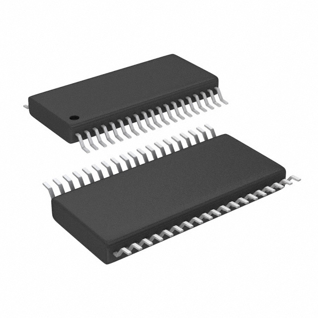
D 38-Pin TSSOP (DBT)
APPLICATIONS
D Notebook PCs
D Medical and Test Equipment
D Portable Instrumentation
DESCRIPTION
The bq2085−V1P2 SBS-compliant gas gauge IC for
battery pack or in-system installation maintains an
accurate record of available charge in Li-ion or Li-polymer
batteries. The bq2085−V1P2 monitors capacity and other
critical parameters of the battery pack and reports the
information to the system host controller over a serial
communication bus. It is designed to work with the
bq29311 analog front-end (AFE) protection IC to maximize
functionality and safety and minimize component count
and cost in smart battery circuits. Using information from
the bq2085−V1P2, the host controller can manage
remaining battery power to extend the system run time as
much as possible.
BLOCK DIAGRAM
Pack+
Charge/Discharge
Power FETs
LDO
Supply Voltage
bq29311
SMBus
bq2085−V1P2
Temp
Sensor
512 Bytes
Config.
FLASH
EPROM
ADC
Voltage
Integrating
ADC
Coulomb
Counting
Glueless
Interface
Cell Inputs
Safety Control
Level
Translator
+
−
+ Li-Ion
− Cells
+
−
Sense
Resistor
(10 mΩ - 20 mΩ)
Pack−
Please be aware that an important notice concerning availability, standard warranty, and use in critical applications of Texas Instruments
semiconductor products and disclaimers thereto appears at the end of this data sheet.
PRODUCTION DATA information is current as of publication date. Products
conform to specifications per the terms of Texas Instruments standard warranty.
Production processing does not necessarily include testing of all parameters.
Copyright 2003, Texas Instruments Incorporated
�bq2085−V1P2
www.ti.com
SLUS590 − DECEMBER 2003
DESCRIPTION (CONTINUED)
The bq2085−V1P2 uses an integrating converter with
continuous sampling for the measurement of battery
charge and discharge currents. Optimized for coulomb
counting in portable applications, the self-calibrating
integrating converter has a resolution better than 3-nVh
and an offset measurement error of less than 1-µV
(typical). For voltage and temperature reporting, the
bq2085−V1P2 uses a 16-bit A-to-D converter. In
conjunction with the bq29311, the onboard ADC also
monitors individual cell voltages in a battery pack and
allows the bq2085−V1P2 to generate the control signals
necessary to implement the cell balancing and the
required safety protection for Li-ion and Li-polymer battery
chemistries.
The bq29311 AFE protection IC provides power to the
bq2085−V1P2 from a 3 or 4 series Li-ion cell stack,
eliminating the need for an external regulator circuit.
TSSOP PACKAGE
(TOP VIEW)
VIN
TS
OC
N/C
N/C
SCLK
N/C
VDDD
RBI
SDATA
VSSD
SAFE
N/C
N/C
SMBC
SMBD
DISP
EVENT
VSSD
The bq2085−V1P2 supports the smart battery data
(SBData) commands and charge-control functions. It
communicates data using the System Management Bus
(SMBus) 2-wire protocol. The data available include the
battery’s remaining capacity, temperature, voltage,
current, and remaining run-time predictions. The
bq2085−V1P2 provides LED drivers and a push-button
input to depict remaining battery capacity from full to empty
in 20%, 25%, or 33% increments with a 3-, 4-, or
5-segment display.
The bq2085−V1P2 contains 512 bytes of internal data
flash memory, which store configuration information. The
information includes nominal capacity and voltage,
self-discharge rate, rate compensation factors, and other
programmable cell-modeling factors used to accurately
adjust remaining capacity for use-conditions based on
time, rate, and temperature. The bq2085−V1P2 also
automatically calibrates or learns the true battery capacity
in the course of a discharge cycle from programmable near
full to near empty levels.
2
1
38
2
37
3
36
4
35
5
34
6
33
7
32
8
31
9
30
10
29
11
28
12
27
13
26
14
25
15
24
16
23
17
22
18
21
19
20
VSSD
N/C
N/C
CLKOUT
VSSA
ROSC
FILT
VDDA
VSSA
VSSA
SR1
SR2
MRST
N/C
LED1
LED2
LED3
LED4
LED5
NC − No internal connection
AVAILABLE OPTIONS
(1)
TA
PACKAGE
38-PIN TSSOP
(DBT)
−20°C to 85°C
bq2085−V1P2DBT(1)
The bq2085−V1P2 is available taped and reeled. Add an R suffix to
the device type (e.g., bq2085−V1P2DBTR) to order tape and reel
version.
�bq2085−V1P2
www.ti.com
SLUS590 − DECEMBER 2003
Terminal Functions
TERMINAL
DESCRIPTION
I/O
NAME
No.
CLKOUT
35
I
32.768-kHz output to the bq29311
DISP
17
I
Display control for the LED drivers LED1 through LED5
FILT
32
I
Analog input connected to the external PLL filter
EVENT
18
I
Input from bq29311 XALERT output
LED1
24
O
LED2
23
O
LED3
22
O
LED4
21
O
LED5
20
O
MRST
LED display segments that each may drive an external LED
26
I
Master reset input that forces the device into reset when held high
N/C
4, 5, 7, 13,
14, 25, 36, 37
−
No connection
OC
3
I
Analog input for auto ADC offset compensation; should be connected to VSSA
RBI
9
I
Register backup that provides backup potential to the bq2085−V1P2 data registers during periods of low
operating voltage. RBI accepts a storage capacitor or a battery input.
ROSC
33
I
Internal time base bias input
SAFE
12
O
Output for additional level of safety protection; e.g., fuse blow.
SCLK
6
O
Communication clock to the bq29311
SDATA
10
I/O
Data transfer to and from bq29311
SMBC
15
I/O
SMBus clock open-drain bidirectional pin used to clock the data transfer to and from the bq2085−V1P2
SMBD
16
I/O
SMBus data open-drain bidirectional pin used to transfer address and data to and from the bq2085−V1P2
SR1
28
I
SR2
27
I
TS
2
I
Thermistor voltage input connection to monitor temperature
VDDA
31
I
Positive supply for analog circuitry
VDDD
8
I
Positive supply for digital circuitry and I/O pins
VIN
Connections for a small-value sense resistor to monitor the battery charge- and discharge-current flow
1
I
Single cell voltage input from the bq29311
VSSA
30, 34
I
Negative supply for analog circuitry
VSSD
11, 19, 38
I
Negative supply for digital circuitry
VSSA
29
I
Negative supply for output circuitry
3
�bq2085−V1P2
www.ti.com
SLUS590 − DECEMBER 2003
ABSOLUTE MAXIMUM RATINGS
over operating free-air temperature range unless otherwise noted(1)
UNIT
Supply voltage range, VDD relative to VSS(2)
−0.3 V to 6 V
Open-drain I/O pins, V(IOD) relative to VSS (2)
−0.3 V to 6 V
Input voltage range to all other pins, VI relative to VSS (2)
−0.3 V to VDD + 0.3V
Operating free-air temperature range, TA
−20°C to 85°C
Storage temperature range, Tstg
−65°C to 150°C
ESD rating
HBM
1.5 kV
CDM
1.5 kV
MM
50 V
(1)
Stresses beyond those listed under “absolute maximum ratings” may cause permanent damage to the device. These are stress ratings only, and
functional operation of the device at these or any other conditions beyond those indicated under “recommended operating conditions” is not
implied. Exposure to absolute-maximum-rated conditions for extended periods may affect device reliability.
(2) VSS refers to the common node of V
(SSA), V(SSD), and V(SSP).
ELECTRICAL CHARACTERISTICS
VDD = 3.0 V to 3.6 V, TA = −20°C to 85°C (unless otherwise noted)
PARAMETER
TEST CONDITIONS
MIN
TYP
MAX
3.0
3.3
3.6
UNIT
VDD
Supply voltage
VDDA and VDDD
V
IDD
Operating current
No flash programming
I(SLP)
Low-power storage mode current
Hibernate mode
V(OLS)
Output voltage low: (LED1−LED5)
I(OLS) = 10 mA
VIL
Input voltage low DISP
VIH
Input voltage high DISP
VOL
Output voltage low SMBC, SMBD, SDATA, SCLK,
EVENT, SAFE
V(ILS)
Input voltage low SMBC, SMBD, SDATA, SCLK, EVENT,
SAFE
V(IHS)
Input voltage high SMBC, SMBD, SDATA, SCLK,
EVENT, SAFE
V(AI)
Input voltage range VIN, TS, OC
Z(AI1)
Input impedance SR1, SR2
0 V–1.0 V
10
MΩ
Z(AI2)
Input impedance VIN, TS, OC
0 V–1.0 V
8
MΩ
450
µA
1
µA
0.4
V
−0.3
0.8
V
2
VCC + 0.3
V
0.4
V
−0.3
0.8
V
1.7
6
V
VSS − 0.3
1.0
IOL = 0.5 mA
V
POWER-ON RESET (see FIGURE 1)
VIT−
Negative-going voltage input
2.1
2.3
2.5
V
Vhys
Power-on reset hysteresis
50
125
210
mV
4
�bq2085−V1P2
www.ti.com
SLUS590 − DECEMBER 2003
2.50
150
2.45
145
140
2.40
VIT−
Vhys
2.35
135
2.30
130
2.25
125
2.20
120
2.15
115
2.10
−20
V hys − Hysteresis Voltage − mV
V IT− − Negative-Going Input Threshold Voltage − V
POR BEHAVIOR
vs
FREE-AIR TEMPERATURE
110
−5
10
25
40
55
70
85
TA − Free-Air Temperature − °C
Figure 1
INTEGRATING ADC CHARACTERISTICS
VDD = 3.0 V to 3.6 V, TA = −20°C to 85°C (unless otherwise noted)
PARAMETER
V(SR)
Input voltage range, V(SR2) and V(SR1)
V(SROS)
Input offset
INL
Integral nonlinearity error
TEST CONDITIONS
VSR = V(SR2) – V(SR1)
MIN
TYP
MAX
–0.3
1.0
UNIT
V
µV
1
0.003%
0.009%
PLL SWITCHING CHARACTERISTICS
VDD = 3.0 V to 3.6 V, TA = −20°C to 85°C (unless otherwise noted)
PARAMETER
t(sp)
(1) The
Start-up
TEST CONDITIONS
MIN
±0.5% frequency error
time (1)
TYP
MAX
2
5
UNIT
ms
frequency error is measured from 32.768 Hz.
Internal Oscillator
VDD = 3.0 V to 3.6 V, TA = −20°C to 85°C (unless otherwise noted)
PARAMETER
f(exo)
Frequency error(1)
f(sxo)
Start-up time (2)
(1)
(2)
TEST CONDITIONS
MIN
−2%
VDD = 3.3 V
−1%
TYP
MAX
UNIT
2%
1%
275
µs
The frequency error is measured from 32.768 Hz.
The start-up time is defined as the time it takes for the oscillator output frequency to be ±1%.
5
�bq2085−V1P2
www.ti.com
SLUS590 − DECEMBER 2003
SMBUS TIMING SPECIFICATIONS
VDD = 3.0 V to 3.6 V, TA = −20°C to 85°C (unless otherwise noted)
PARAMETER
TEST CONDITIONS
MIN
TYP
UNIT
100
kHz
SMBus operating frequency
Slave mode, SMBC 50% duty cycle
FMAS
SMBus master clock frequency
Master mode, no clock low slave extend
TBUF
Bus free time between start and stop
4.7
µs
THD:STA
Hold time after (repeated) start
4.0
µs
TSU:STA
Repeated start setup time
4.7
µs
TSU:STO
Stop setup time
4.0
µs
THD:DAT
Data hold time
TSU:DAT
Data setup time
TTIMEOUT
Error signal/detect
TLOW
Clock low period
10
MAX
FSMB
51.2
Receive mode
0
Transmit mode
300
kHz
ns
250
See
(1)
ns
25
35
ms
µs
4.7
THIGH
Clock high period
See
50
µs
TLOW:SEXT
Cumulative clock low slave extend time
See (3)
25
ms
TLOW:MEXT
Cumulative clock low master extend time
See (4)
10
ms
TF
Clock/data fall time
See (5)
300
ns
TR
Clock/data rise time
See (6)
1000
ns
(1)
(2)
(3)
(4)
(5)
(6)
(2)
4.0
The bq2085−V1P2 times out when any clock low exceeds TTIMEOUT
THIGH Max. is minimum bus idle time. SMBC = 1 for t > 50 µs causes reset of any transaction involving bq2085−V1P2 that is in progress.
TLOW:SEXT is the cumulative time a slave device is allowed to extend the clock cycles in one message from initial start to the stop.
TLOW:MEXT is the cumulative time a master device is allowed to extend the clock cycles in one message from initial start to the stop.
Rise time TR = (VILMAX − 0.15 V) to (VIHMIN + 0.15 V).
Fall time TF = 0.9 VDD to (VILMAX − 0.15 V).
DATA FLASH MEMORY SWITCHING CHARACTERISTICS
VDD = 3.0 V to 3.6 V, TA = −20°C to 85°C (unless otherwise noted)
PARAMETER
TEST CONDITIONS
Data retention
See (1)
Flash programming write-cycles
See (1)
t(WORDPROG)
Word programming time
See (1)
I(DDPROG)
Flash-write supply current
See (1)
t(RETENSION)
(1)
MIN
TYP
MAX
10
UNIT
Years
105
Cycles
2
ms
14
16
mA
TYP
MAX
UNIT
10
100
nA
Specified by design. Not production tested.
Register Backup
PARAMETER
I(RBI)
RBI data-retention input current (1)
V(RBI)
RBI data-retention voltage
(1)
6
Specified by design. Not production tested.
TEST CONDITIONS
MIN
VRB > 3.0 V, VDD < VIT
1.3
V
�bq2085−V1P2
www.ti.com
SLUS590 − DECEMBER 2003
SMBUS TIMING DIAGRAMS
TLOW
SCLK
TR
THIGH
THD:STA
THD:STA
TF
TSU:STA
TSU:STO
TSU:DAT
THD:DAT
SDATA
TBUF
P
S
S
Start
P
Stop
TLOW:SEXT
SCLKACK(1)
TLOW:MEXT
SCLKACK(1)
TLOW:MEXT
TLOW:MEXT
SCLK
SDATA
(1)
SCLKACK is the acknowledge-related clock pulse generated by the master.
Figure 2. SMBus Timing Diagram
FUNCTIONAL DESCRIPTION
Internal Oscillator Function
The internal oscillator performance is additionally dependent on the tolerance of the 113k resistor connected
between RSOC (pin 33) and VSSA (pin 34). It is recommended that this resistor be as close to the
bq2085−V1P2 as possible and that it have a specification of ±0.1% tolerance and ±50 ppm temperature drift
or better. The layout of the PCBA is also an additional contributing factor to performance degradation.
The average temperature drift error of the oscillator function over a learning charge or discharge cycle
introduces an equal capacity prediction error in a learned full charge capacity (FCC).
General Operation
The bq2085−V1P2 determines battery capacity by monitoring the amount of charge input or removed from a
rechargeable battery. In addition to measuring charge and discharge, the bq2085−V1P2 measures battery
voltage, temperature, and current, estimates battery self-discharge, and monitors the battery for low-voltage
thresholds. The bq2085−V1P2 measures charge and discharge activity by monitoring the voltage across a
small-value series sense resistor between the battery’s negative terminal and the negative terminal of the
battery pack. The available battery charge is determined by monitoring this voltage and correcting the
measurement for environmental and operating conditions.
The bq2085−V1P2 interfaces with the bq29311 to perform battery protection, cell balancing, and voltage
translation functions.
The bq2085−V1P2 can accept any NTC thermistor (default is Semitec 103AT) for temperature measurement
or can be configured to use its internal temperature sensor. The bq2085−V1P2 uses temperature to monitor
the battery pack and to compensate the self-discharge estimate.
Measurements
The bq2085−V1P2 uses an integrating sigma-delta analog-to-digital converter (ADC) for current measurement
and a second sigma delta ADC for battery voltage and temperature measurement. Voltage, current, and
temperature measurements are made every second.
7
�bq2085−V1P2
www.ti.com
SLUS590 − DECEMBER 2003
Charge and Discharge Counting
The integrating ADC measures the charge and discharge flow of the battery by monitoring a small-value sense
resistor between the SR1 and SR2 pins as shown in the schematic. The integrating ADC measures bipolar
signals from −0.3 to 1.0 V. The bq2085−V1P2 detects charge activity when VSR = V(SR1)–V(SR2) is positive and
discharge activity when VSR = V(SR1)–V(SR2) is negative. The bq2085−V1P2 continuously integrates the signal
over time, using an internal counter. The fundamental rate of the counter is 2.6 nVh. The bq2085−V1P2 updates
Remaining Capacity() with the charge or discharge accumulated in this internal counter once every second.
Offset Calibration
The bq2085−V1P2 provides an autocalibration feature to cancel the voltage offset error across SR1 and SR2
for maximum charge measurement accuracy. The bq2085−V1P2 performs autocalibration when the SMBus
lines stay low for a minimum of 20 s. The bq2085−V1P2 is capable of automatic offset calibration down to 1 µV.
Digital Filter
The bq2085−V1P2 does not measure charge or discharge counts below the digital filter threshold. The digital
filter threshold is programmed in the Digital Filter DF 0x2b. Set it sufficiently high to prevent false signal detection
with no charge or discharge flowing through the sense resistor.
Voltage
While monitoring SR1 and SR2 for charge and discharge currents, the bq2085−V1P2 monitors the individual
series cell voltages through the bq29311. The bq2085−V1P2 configures the bq29311 to present the selected
cell to the VCELL pin of the bq29311. Therefore, connect the VCELL pin to VIN of the bq2085−V1P2. The
internal ADC of the bq2085−V1P2 then measures the voltage and scales it appropriately. The bq2085−V1P2
then reports the Voltage( ) and the individual cell voltages in VCELL1, VCELL2, VCELL3, and VCELL4 located
in 0x3c−0x3f.
Current
The bq2085−V1P2 uses the SR1 and SR2 inputs to measure and calculate the battery charge and discharge
current as represented in the data register Current().
Temperature
The TS input of the bq2085−V1P2 in conjunction with an NTC thermistor measures the battery temperature
as shown in the schematic. The bq2085−V1P2 reports temperature in Temperature( ).
The bq2085−V1P2 can also be configured to use its internal temperature sensor by setting the IT bit in Misc
Configuration DF 0x2a. Data flash locations DF 0xa4 through DF 0xad also have to be changed to prescribed
values if the internal temperature sensor option is selected.
Table 1. Data Flash Settings for Internal or External Temperature Sensor
LABEL
LOCATION
INTERNAL TEMP SENSOR SETTING
EXTERNAL TEMP SENSOR SETTING
(Semitec 103AT)
Dec (Hex)
Dec (Hex)
Dec (Hex)
Misc. Configuration
42 (0x2a)
Bit 7 = 1
Bit 7 = 0
TS Const1 A3
164/5 (0xa4/5)
0 (0x0000)
−28285 (0x9183)
TS Const2 A2
166/7 (0xa6/7)
0 (0x0000)
20848 (0x5170)
TS Const3 A1
168/9 (0xa8/9)
−11136 (0xd480)
−7537 (0xe28f)
TS Const4 A0
170/1 (0xaa/b)
5754 (0x1666)
4012 (0x0fac)
Min Temp AD
172/3 (0xac/d)
0 (0x0000)
0 (0x0000)
Max Temp
174/5 (0xae/f)
5734 (0x1666)
4012 (0x0fac)
If AD < Min Temp AD then Temp = Max Temp
Else
Temp = ([A3 × AD × 2^ − 16 + A2] × AD × 2^ − 16 + A1) × AD 2^ −16 + A0
8
�bq2085−V1P2
www.ti.com
SLUS590 − DECEMBER 2003
Gas Gauge Operation
General
The operational overview in Figure 3 illustrates the gas gauge operation of the bq2085−V1P2. Table 3
describes the bq2085−V1P2 registers.
Inputs
Charge
Current
Battery Electronics
Load Estimate
Discharge
Current
Charge
Efficiency
Compensation
Temperature
Compensation
−
Main Counters and
Capacity Reference (FCC)
Self-Discharge
Timer
+
−
−
Remaining
Capacity
(RM)
+
≤
Full
Charge
Capacity
(FCC)
Qualified
Transfer
+
+
Discharge
Count
Register
(DCR)
Temperature, Other Data
Outputs
Chip-Controlled
Available Charge
LED Display
Two-Wire
Serial Port
Figure 3. bq2085−V1P2 Operational Overview
The bq2085−V1P2 accumulates a measure of charge and discharge currents and estimates self-discharge of
the battery. The bq2085−V1P2 compensates the charge current measurement for temperature and
state-of-charge of the battery. The bq2085−V1P2 also adjusts the self-discharge estimation based on
temperature.
The main charge counter RemainingCapacity( ) (RM) represents the available capacity or energy in the battery
at any given time. The bq2085−V1P2 adjusts RM for charge, self-discharge, and other compensation factors.
The information in the RM register is accessible through the SMBus interface and is also represented through
the LED display.
The FullChargeCapacity( ) (FCC) register represents the last measured full discharge of the battery. It is used
as the battery full-charge reference for relative capacity indication. The bq2085−V1P2 updates FCC after the
battery undergoes a qualified discharge from nearly full to a low battery level. FCC is accessible through the
SMBus interface.
The discharge count register (DCR) is a non-accessible register that tracks discharge of the battery. The
bq2085−V1P2 uses the DCR register to update the FCC register if the battery undergoes a qualified discharge
from nearly full to a low battery level. In this way, the bq2085−V1P2 learns the true discharge capacity of the
battery under system use conditions.
Main Gas-Gauge Registers
The gas-gauge register functions are described in Table 3.
9
�bq2085−V1P2
www.ti.com
SLUS590 − DECEMBER 2003
RemainingCapacity( ) (RM)
RM represents the remaining capacity in the battery. The bq2085−V1P2 computes RM in units of either mAh
or 10 mWh depending on the selected mode. See Battery Mode( ) (0x03) for units configuration.
RM counts up during charge to a maximum value of FCC and down during discharge and self-discharge to a
minimum of 0. In addition to charge and self-discharge compensation, the bq2085−V1P2 calibrates RM at three
low-battery-voltage thresholds, EDV2, EDV1, and EDV0 and three programmable midrange thresholds
VOC25, VOC50, and VOC75. This provides a voltage-based calibration to the RM counter.
DesignCapacity( ) (DC)
DC is the user-specified battery full capacity. It is calculated from Pack Capacity DF 0x31-0x32 and is
represented in units of mAh or 10 mWh. It also represents the full-battery reference for the absolute display
mode.
FullChargeCapacity( ) (FCC)
FCC is the last measured discharge capacity of the battery. It is represented in units of either mAh or 10 mWh,
depending on the selected mode. On initialization, the bq2085−V1P2 sets FCC to the value stored in Last
Measured Discharge DF 0x35-0x36. During subsequent discharges, the bq2085−V1P2 updates FCC with the
last measured discharge capacity of the battery. The last measured discharge of the battery is based on the
value in the DCR register after a qualified discharge occurs. Once updated, the bq2085−V1P2 writes the new
FCC value to data flash in mAh to Last Measured Discharge. FCC represents the full battery reference for the
relative display mode and relative state of charge calculations.
Discharge Count Register (DCR)
The DCR register counts up during discharge, independent of RM. DCR counts discharge activity, battery load
estimation, and self-discharge increment. The bq2085−V1P2 initializes DCR, at the beginning of a discharge,
to FCC − RM when RM is within the programmed value in Near Full DF 0x2f. The DCR initial value of FCC −
RM is reduced by FCC/128 if SC = 1 (bit 5 in Gauge Configuration) and is not reduced if SC = 0. DCR stops
counting when the battery voltage reaches the EDV2 threshold on discharge.
Capacity Learning (FCC Update) and Qualified Discharge
The bq2085−V1P2 updates FCC with an amount based on the value in DCR if a qualified discharge occurs.
The new value for FCC equals the DCR value plus the programmable nearly full and low battery levels,
according to the following equation:
FCC (new) + DCR (final) + DCR (initial) ) Measured Discharge to EDV2 ) (FCC
Battery Low%)
(1)
Battery Low % = (value stored in DF 0x2e) ÷ 2.56
A qualified discharge occurs if the battery discharges from RM ≥ FCC − Near Full to the EDV2 voltage threshold
with the following conditions:
D No valid charge activity occurs during the discharge period. A valid charge is defined as a charge of 10 mAh into
the battery.
D No more than 256 mAh of self-discharge or battery load estimation occurs during the discharge period.
D The temperature does not drop below the low temperature thresholds programmed in Learning Low Temp DF
0x9b during the discharge period.
D The battery voltage reaches the EDV2 threshold during the discharge period and the voltage is greater than or
equal to the EDV2 threshold minus 256 mV when the bq2085−V1P2 detected EDV2.
D No midrange voltage correction occurs during the discharge period.
D Current remains ≥ 3C/32 when EDV2 or Battery Low % level is reached.
D No overload condition exists when EDV2 threshold is reached or if RM( ) has dropped to Battery Low% *FCC.
The bq2085−V1P2 sets VDQ=1 in pack status when qualified discharge begins. The bq2085−V1P2 sets
VDQ=0 if any disqualifying condition occurs. FCC cannot be reduced by more than 256 mAh or increased by
more than 512 mAh during any single update cycle. The bq2085−V1P2 saves the new FCC value to the data
flash within 4 seconds of being updated.
10
�bq2085−V1P2
www.ti.com
SLUS590 − DECEMBER 2003
End-of-Discharge Thresholds and Capacity Correction
The bq2085−V1P2 monitors the battery for three low-voltage thresholds, EDV0, EDV1, and EDV2. The EDV
thresholds can be programmed for determination based on the overall pack voltage or an individual cell level.
The EDVV bit in Pack Configuration DF 0x28 configures the bq2085−V1P2 for overall voltage or single-cell EDV
thresholds. If programmed for single cell EDV determination, the bq2085−V1P2 determines EDV on the basis
of the lowest single-cell voltage. Fixed EDV thresholds can be programmed in EMF/EDV0 DF 0x84-0x85, EDV
C0 Factor/EDV1 DF 0x86-0x87, and EDV R Factor/EDV2 DF 0x88-0x89. If the CEDV bit in Gauge
Configuration DF 0x29 is set, automatic EDV compensation is enabled and the bq2085−V1P2 computes the
EDV0, EDV1, and EDV2 thresholds based on the values in DF 0x84-0x8d and the battery’s current discharge
rate and temperature. The bq2085−V1P2 disables EDV detection if Current( ) exceeds the Overload Current
threshold programmed in DF 0x58 − DF 0x59. The bq2085−V1P2 resumes EDV threshold detection after
Current( ) drops below the Overload Current threshold. Any EDV threshold detected is reset after charge is
applied and VDQ is cleared after 10mAh of charge.
Table 2. State of Charge Based on Low Battery Voltage
THRESHOLD
RELATIVE STATE OF CHARGE
EDV0
0%
EDV1
3%
EDV2
Battery Low %
The bq2085−V1P2 uses the EDV thresholds to apply voltage-based corrections to the RM register according
to Table 1. The bq2085−V1P2 performs EDV-based RM adjustments with Current( ) ≥ C/32. No EDVs are set
if current < C/32. The bq2085−V1P2 adjusts RM as it detects each threshold. If the voltage threshold is reached
before the corresponding capacity on discharge, the bq2085−V1P2 reduces RM to the appropriate amount as
shown in Table 2. This reduction occurs only if current ≥ C/32 when the EDV threshold is detected. If RM
reaches the capacity level before the voltage threshold is reached on discharge, the bq2085−V1P2 prevents
RM from decreasing further until the battery voltage reaches the corresponding threshold only on a full learning
cycle discharge. RM is not held at the associated EDV percentage on a nonlearning discharge cycle (VDQ=0)
or if current < C/32.
If Battery Low % is set to zero, EDV1 and EDV0 corrections are disabled.
Table 3. bq2085−V1P2 Register Functions
FUNCTION
COMMAND CODE
ACCESS
UNITS
ManufacturerAccess
0x00
read/write
NA
RemainingCapacityAlarm
0x01
read/write
mAh, 10 mWh
RemainingTimeAlarm
0x02
read/write
minutes
BatteryMode
0x03
read/write
NA
AtRate
0x04
read/write
mA, 10mW
AtRateTimeToFull
0x05
read
minutes
AtRateTimeToEmpty
0x06
read
minutes
AtRateOK
0x07
read
Boolean
Temperature
0x08
read
0.1°K
Voltage
0x09
read
mV
Current
0x0a
read
mA
AverageCurrent
0x0b
read
mA
MaxError
0x0c
read
percent
RelativeStateOfCharge
0x0d
read
percent
AbsoluteStateOfCharge
0x0e
read
percent
RemainingCapacity
0x0f
read
mAh, 10 mWh
11
�bq2085−V1P2
www.ti.com
SLUS590 − DECEMBER 2003
Table 3. bq2085−V1P2 Register Functions (Continued)
FUNCTION
COMMAND CODE
ACCESS
UNITS
FullChargeCapacity
0x10
read
mAh, 10 mWh
RunTimeToEmpty
0x11
read
minutes
AverageTimeToEmpty
0x12
read
minutes
AverageTimeToFull
0x13
read
minutes
ChargingCurrent
0x14
read
mA
ChargingVoltage
0x15
read
mV
Battery Status
0x16
read
NA
CycleCount
0x17
read
cycles
DesignCapacity
0x18
read
mAh, 10 mWh
DesignVoltage
0x19
read
mV
SpecificationInfo
0x1a
read
NA
ManufactureDate
0x1b
read
NA
0x1c
read
integer
0
0
SerialNumber
Reserved
0x1d-0x1f
ManufacturerName
0x20
read
string
DeviceName
0x21
read
string
DeviceChemistry
0x22
read
string
ManufacturerData
0x23
read
string
Pack status
0x2f (LSB)
read
NA
Pack configuration
0x2f (MSB)
read
NA
VCELL4
0x3c
read
mV
VCELL3
0x3d
read
mV
VCELL2
0x3e
read
mV
VCELL1
0x3f
read
mV
Self-Discharge
The bq2085−V1P2 estimates the self-discharge of the battery to maintain an accurate measure of the battery
capacity during periods of inactivity. The bq2085−V1P2 makes self-discharge adjustments to RM( ) every 1/4
seconds when awake and periodically when in sleep mode. The period is determined by Sleep Timer DF 0xe7.
The self-discharge estimation rate for 25°C is doubled for each 10 degrees above 25°C or halved for each 10
degrees below 25°C. The following table shows the relation of the self-discharge estimation at a given
temperature to the rate programmed for 25°C (Y% per day programmed in DF 0x2c).
Table 4. Self-Discharge for Rate Programmed
12
TEMPERATURE
(°C)
SELF-DISCHARGE RATE
Temp < 10
1/4 Y% per day
10 ≤ Temp EDV2 threshold (discharging)
1
Voltage ≤ EDV2 threshold
SS
The SS bit indicates the seal state of the bq2085−V1P2.
36
0
The bq2085−V1P2 is in the unsealed state.
1
The bq2085−V1P2 is in the sealed state.
�www.ti.com
bq2085−V1P2
SLUS590 − DECEMBER 2003
VDQ
The VDQ bit indicates if the present discharge cycle is valid for an FCC update.
0
Discharge cycle not valid
1
Discharge cycle valid
SOV
The SOV bit indicates that the safety output limits have been exceeded. Once set, the flag stays set until the
bq2085−V1P2 is reset.
0
Safety limits not exceeded
1
Safety limits exceeded
CVOV
The CVOV bit indicates that a protection limit has been exceeded. It is set on a Prolonged Overcurrent,
Overvoltage, or Overtemperature condition. The bit is not latched and merely reflects the present fault status.
0
No secondary protection limits exceeded
1
A secondary protection limit exceeded
CVUV
The CVUV bit indicates that a protection limit has been exceeded. It is set on an overload or overdischarge
condition. The bit is not latched and merely reflects the present fault status.
0
No secondary protection limits exceeded
1
A secondary protection limit exceeded
VCELL4-VCELL1 (0x3c-0x3f)
These functions return the calculated individual cell voltages in mV.
DATA FLASH
General
The bq2085−V1P2 accesses the internal data flash during reset and when storing historical data. The data flash
stores basic configuration information for use by the bq2085−V1P2. The data flash must be programmed
correctly for proper bq2085−V1P2 operation.
Memory Map
Table 13 shows the memory map for the data flash. It shows the default programming for the bq2085−V1P2.
The default programming reflects example data for a 3s2p Li-Ion battery pack with a 0.02 Ω sense resistor. The
data flash must be reprogrammed to meet the requirements of individual applications.
37
�bq2085−V1P2
www.ti.com
SLUS590 − DECEMBER 2003
Table 13. Data Flash Memory Map
DATA FLASH ADDRESS
HIGH BYTE
DATA
NAME
MSB
LSB
0x00
0x01
Remaining Time Alarm
10 minutes
00
0a
0x02
0x03
Remaining Capacity Alarm
360 mAh
01
68
0x04
0x05
Design Voltage
10800 mV
2a
30
0x06
0x07
Specification Information
v1.1/PEC
00
31
0x08
0x09
Manufacture Date
2/15/02=11343
2c
4f
0x0a
0x0b
Serial Number
1
00
01
0x0c
0x0d
Cycle Count
0
00
00
0x0e
Manufacturer Name Length
11
0b
0x0f
Character 1
T
54
0x10
Character 2
e
45
0x11
Character 3
x
58
0x12
Character 4
a
41
0x13
Character 5
s
53
0x14
Character 6
0x15
Character 7
I
49
0x16
Character 8
n
4e
0x17
Character 9
s
53
0x18
Character 10
t
54
0x19
Character 11
.
2e
0x1a
Device Name Length
6
06
0x1b
Character 1
b
42
0x1c
Character 2
q
51
0x1d
Character 3
2
32
0x1e
Character 4
0
30
0x1f
Character 5
8
38
0x20
Character 6
5
35
0x21
Character 7
—
00
0x22
Device Chemistry Length
4
04
0x23
Character 1
L
4c
0x24
Character 2
I
49
0x25
Character 3
O
4f
0x26
Character 4
N
4e
0x27
Manufacturer Data Length
12
09
0x28
Pack Configuration
DMODE, LED1, CC1
c2
0x29
Gauge Configuration
CSYNC
40
0x2a
Misc Configuration
VOD
01
0x2b
Digital Filter
9860 nV
22
0x2c
Self-Discharge Rate
0.2%
14
0x2d
Electronics Load
0 mA
00
0x2e
Battery Low %
7.03%
12
Near Full
200 mAh
0x2f
LOW BYTE
LI-ION EXAMPLE
0x30
20
00
c8
NOTE: Reserved locations must be set as shown. Locations marked with an * are typical calibration values that can be adjusted for maximum
accuracy. For these locations the table shows the appropriate default or initial setting.
38
�bq2085−V1P2
www.ti.com
SLUS590 − DECEMBER 2003
Table 13. Data Flash Memory Map (Continued)
DATA FLASH ADDRESS
HIGH BYTE
DATA
NAME
LOW BYTE
LI-ION EXAMPLE
MSB
LSB
0x31
0x32
Design Capacity
3600 mAh
0e
10
0x33
0x34
Reserved
0
00
00
0x35
0x36
Last Measured Discharge
3600 mAh
0e
10
0x37
0x38
Cycle Count Threshold
2880 mAh
0b
40
0x39
0x3a
Charging Voltage
12600 mV
31
38
0x3b
0x3c
Precharge Voltage
8000 mV
1f
40
0x3d
0x3e
Fast-Charging Current
2500 mA
09
c4
0x3f
0x40
Maintenance Charging Current
0 mA
00
00
0x41
0x42
Precharge Current
100 mA
00
64
0x43
Precharge Temp
9.6°C
0x44
Reserved
1e
0x45
Reserved
00
0x46
Fast Charge Termination %
100%
ff
0x47
Fully Charged Clear %
95%
5f
60
0x48
0x49
Current Taper Threshold
240 mA
00
f0
0x4a
0x4b
Current Taper Qual Voltage
100 mV
00
64
0x4c
Reserved
0x4d
0x4e
Reserved
0x4f
Maximum Overcharge
0x50
Reserved
0x51
Charge Efficiency
0x52
Reserved
0x53
28
0x54
0x55
40
300 mAh
01
2c
02
100%
ff
64
MaxTemperature
54.6°C
Temperature Hysteresis
5°C
0x56
0x57
Reserved
0x58
0x59
Overload Current
0x5a
0x5b
Over Voltage Margin
0x5c
0x5d
Overcurrent Margin
0x5e
0x5f
Reserved
0x60
0x61
Cell Over Voltage
0x62
0x63
0x64
0x65
0x66
0x67
Reserved
0x68
0x69
Safety Over Voltage
20000 mV
0x6a
0x6b
Safety Over Temperature
70°C
02
22
32
01
ae
5000 mA
13
88
208 mV
00
d0
500 mA
01
f4
01
00
4350 mV
10
fe
Cell Under Voltage
2300 mV
08
fc
Terminate Voltage
8500 mV
21
34
00
00
4e
20
02
bc
0x6c
Reserved
ef
0x6d
Reserved
03
0x6e
0x6f
VOC75
11890 mV
2e
72
0x70
Reserved
bf
0x71
Reserved
56
NOTE: Reserved locations must be set as shown. Locations marked with an * are typical calibration values that can be adjusted for maximum
accuracy. For these locations the table shows the appropriate default or initial setting.
39
�bq2085−V1P2
www.ti.com
SLUS590 − DECEMBER 2003
Table 13. Data Flash Memory Map (Continued)
DATA FLASH ADDRESS
HIGH BYTE
LOW BYTE
0x72
0x73
DATA
NAME
LI-ION EXAMPLE
MSB
Reserved
0x74
VOC50
LSB
40
11430 mV
2c
a6
0x75
Reserved
7f
0x76
Reserved
3d
0x77
0x78
Reserved
0x79
VOC25
27
11270 mV
2c
06
0x7a
Reserved
3f
0x7b
Reserved
24
0x7c
Reserved
0e
0x7c
Reserved
14
0x7e
Reserved
40
0x7f
0x80
Reserved
0b
e1
0x81
0x82
Reserved
0b
68
0x83
Reserved
19
0x84
0x85
EMF/EDV0
3000 mV
0b
b8
0x86
0x87
EDV C0 Factor/EDV1
3250 mV
0c
b2
0x88
0x89
EDV R0 Factor/EDV2
3400 mV
0d
48
0x8a
0x8b
EDV T0 Factor
0
00
00
0x8c
0x8d
EDV R1 Factor
0
00
00
0x8e
EDV TC Factor
0
00
0x8f
EDV C1 Factor
0
00
0x90
Reserved
08
0x91
Reserved
9b
0x92
Reserved
c7
0x93
Reserved
64
0x94
Reserved
14
0x95
0x96
Reserved
02
00
0x97
0x98
Reserved
01
00
0x99
Reserved
08
0x9a
Reserved
02
0x9b
Learning Low Temp
0x9c
Reserved
11.9°C
77
0a
0x9d
0x9e
Reserved
01
80
0x9f
0xa0
Reserved
01
00
0xa1
Reserved
08
0xa2
Reserved
18
0xa3
Reserved
14
0xa4
0xa5
TS Const 1
91
83
0xa6
0xa7
TS Const 2
51
70
0xa8
0xa9
TS Const 3
e2
8f
0xaa
0xab
TS Const 4
0f
ac
NOTE: Reserved locations must be set as shown. Locations marked with an * are typical calibration values that can be adjusted for maximum
accuracy. For these locations the table shows the appropriate default or initial setting.
40
�bq2085−V1P2
www.ti.com
SLUS590 − DECEMBER 2003
Table 13. Data Flash Memory Map (Continued)
DATA FLASH ADDRESS
HIGH BYTE
DATA
NAME
LOW BYTE
LI-ION EXAMPLE
MSB
LSB
0xac
0xad
TS Const 5
00
00
0xae
0xaf
Reserved
0f
ac
0xb0
Reserved
32
0xb1
AFE Brnout Shutdn
Shutdown = 6.475, Brownout = 7.975 V
00
0xb2
AFE Over Curr Dsg
140 mV
12
0xb3
AFE Over Curr Chg
70 mV
04
0xb4
AFE Over Curr Delay
Charge = 31 ms, Discharge = 31 ms
0xb5
Reserved
0xb6
AFE Short Circ Thrsh
275 mV
ff
00
07
AFE Short Circuit Delay
61 µs (charge and discharge)
0xb8
0xb9
AFE Vref*
9750 mV
26
16
0xba
0xbb
Sense Resistor Gain*
0.02 Ω
3b
d0
0xbc
0xbd
CC Delta*
0.0001298 mAh
94
08
0xbe
0xbf
CC Delta*
b1
c0
0xb7
0xc0
0xc1
11
Reserved
0xc2
fa
CC Offset*
1528
0xc3
DSC Offset*
15
0xc4
ADC Offset*
16
11
0xc5
Temperature Offset*
0
00
Board Offset*
0
0xc6
05
f8
10
00
0xc7
0xc8
Reserved
00
40
0xc9
0xca
Reserved
01
00
0xcb
0xcc
Reserved
0xcd
0xce
Version
05
1.2
Reserved
01
20
00
32
0xcf
0xd0
Cell Over Voltage Reset
4150 mV
10
36
0xd1
0xd2
Cell Under Voltage Reset
3000 mV
0b
b8
0xd3
0xd4
AFE Fail Limit
2 counts
00
02
0xd5
0xd6
Reserved
0xd7
0xd8
Cell Balance Thresh
0xd9
0xda
0xdb
0xdc
ff
ff
3900 mV
0f
3c
Cell Balance Window
100 mV
00
64
Cell Balance Min
40 mV
Cell Balance Interval
20 seconds
28
14
0xdd
0xde
Reserved
a5
5a
0xdf
0xd0
Reserved
7a
43
0xe1
0xe2
Reserved
20
83
0xe3
Reserved
0xe4
AFE Check Time
0 seconds
00
00
0xe5
Sleep Current Thresh
2 mA
04
0xe6
Sleep Current Time
20 seconds
14
0xe7
Sleep Time
100 seconds
64
NOTE: Reserved locations must be set as shown. Locations marked with an * are typical calibration values that can be adjusted for maximum
accuracy. For these locations the table shows the appropriate default or initial setting.
41
�bq2085−V1P2
www.ti.com
SLUS590 − DECEMBER 2003
PROGRAMMING INFORMATION
DATA FLASH PROGRAMMING
The following sections describe the function of each data flash location and how the data is to be stored.
Fundamental Parameters
Sense Resistor Value
The 32-bit CC Delta DF 0xbc−0xbf corrects the coulomb counter for sense resistor variations. It represents the
gain factor for the coulomb counter.
The 16-bit Sense Resistor Gain in DF 0xba-0xbb scales each integrating converter conversion to mAh. The
Current( ) related measurement Sense Resistor Gain is based on the resistance of the series sense resistor.
The following formula computes a nominal or starting value for Sense Resistor Gain from the sense resistor
value.
(2)
Sense Resistor Gain + 306.25
Rs
Digital Filter
The desired digital filter threshold, VDF (V), is set by the value stored in Digital Filter DF 0x2b.
Digital Filter + VDF
290 nV
(3)
Cell and Pack Characteristics
Battery Pack Capacity and Voltage
Pack capacity in mAh units is stored in Design Capacity, DF 0x31−0x32. In mAh mode, the bq2085−V1P2
copies Design Capacity to DesignCapacity( ). In mWh mode, the bq2085−V1P2 multiplies Design Capacity by
Design Voltage DF 0x04−0x05 to calculate DesignCapacity( ) scaled to 10 mWh. Design Voltage is stored in
mV.
The initial value for Last Measured Discharge, in mAh, is stored in DF 0x35−0x36. Last Measured Discharge
is modified over the course of pack usage to reflect cell aging under the particular use conditions. The
bq2085−V1P2 updates Last Measured Discharge in mAh after a capacity learning cycle. The bq2085−V1P2
uses the Last Measured Discharge value to calculate FullChargeCapacity( ) in units of mAh or 10 mWh.
Remaining Time and Capacity Alarms
Remaining Time Alarm in DF 0x00-0x01 and Remaining Capacity Alarm in 0x02-0x03 set the alarm thresholds
used in the SMBus command codes 0x01 and 0x02, respectively. Remaining Time Alarm is stored in minutes
and Remaining Capacity Alarm in units of mAh or 10 mWh, depending on the BatteryMode( ) setting.
EDV Thresholds and Near Full Percentage
The bq2085−V1P2 uses three pack-voltage thresholds to provide voltage-based warnings of low battery
capacity. The bq2085−V1P2 uses the values stored in data flash for the EDV0, EDV1, and EDV2 values or
calculates the three thresholds from a base value and the temperature, capacity, and rate adjustment factors
stored in data flash. If EDV compensation is disabled then EDV0, EDV1, and EDV2 are stored directly in mV
in DF 0x84−0x85, DF 0x86−0x87, and DF 0x88−0x89, respectively.
For capacity correction at EDV2, Battery Low % DF 0x2e can be set at a desired state-of-charge,
STATEOFCHARGE%, in the range of 3-19%. Typical values for STATEOFCHARGE% are 5-7%, representing
5-7% capacity.
Battery Low % = (STATEOFCHARGE% • 2.56)
(4)
The bq2085−V1P2 updates FCC if a qualified discharge occurs from a near-full threshold of FCC − Near Full,
until EDV2 condition is reached. The desired near-full threshold window is programmed in Near Full in DF 0x2f,
0x30 in mAh.
42
�bq2085−V1P2
www.ti.com
SLUS590 − DECEMBER 2003
EDV Discharge Rate and Temperature Compensation
If EDV compensation is enabled, the bq2085−V1P2 calculates battery voltage to determine EDV0, EDV1, and
EDV2 thresholds as a function of battery capacity, temperature, and discharge load. The general equation for
EDV0, EDV1, and EDV2 calculation is
EDV0,1,2 = n (EMF • FBL - | ILOAD | • R0 • FTZ)
(5)
EMF is a no-load cell voltage higher than the highest cell EDV threshold computed. EMF is programmed in mV in
EMF/EDV1 DF 0x84−0x85.
ILOAD is the current discharge load magnitude.
n = the number of series cells
FBL is the factor that adjusts the EDV voltage for battery capacity and temperature to match the no-load
characteristics of the battery.
FBL = f ( C0, C + C1, T )
(6)
C (either 0%, 3%, or Battery Low % for EDV0, EDV1, and EDV2, respectively) and C0 are the capacity- related
EDV adjustment factors. C0 is programmed in EDV C0 Factor/EDV1 DF 0x86−87. C1 is the desired residual
battery capacity remaining at EDV0 (RM = 0). The C1 factor is stored in EDV C1 Factor DF 0x8f.
T is the current temperature in °K.
R0 • FTZ represents the resistance of a cell as a function of temperature and capacity.
FTZ = f ( R1 , T0, T, C + C1, TC)
(7)
R0 is the first order rate dependency factor stored in EDV R0 Factor/EDV2 DF 0x88−0x89.
T is the current temperature; C is the battery capacity relating to EDV0, EDV1, and EDV2.
R1 adjusts the variation of impedance with battery capacity. R1 is programmed in EDV R1 Rate Factor DF
0x8c-0x8d.
T0 adjusts the variation of impedance with battery temperature. T0 is programmed in EDV T0 Rate Factor DF
0x8a−0x8b.
TC adjusts the variation of impedance for cold temperatures (T < 23°C). TC is programmed in EDV TC DF 0x8e.
Typical values for the EDV compensation factors, based on overall pack voltages for a Li-lon 3s2p 18650 pack,
are
EMF = 11550/3
T0 = 4475
C0 = 235
C1 = 0
R0 = 5350/3
R1 = 250
TC = 3
The graphs in Figures 8 and 9 show the calculated EDV0, EDV1, and EDV2 thresholds versus capacity using
the typical compensation values for different temperatures and loads for a Li-Ion 3s2p 18650 pack. The
compensation values vary widely for different cell types and manufacturers and must be matched exactly to
the unique characteristics for optimal performance.
43
�bq2085−V1P2
www.ti.com
SLUS590 − DECEMBER 2003
VOLTAGE
vs
CAPACITY
VOLTAGE
vs
CAPACITY
11.5
11.5
Battery Low % = 7%
Load = 500 mA
11.0
20°C
EDV2
EDV2
10.5
45°C
10.5
Battery Low % = 7%
TA = 35°C
11.0
500 mA
EDV1
V − Voltage − V
V − Voltage − V
EDV1
10.0
9.5
9.0
8.5
10.0
1A
2A
9.5
9.0
8.5
8.0
8.0
7.5
EDV0
7.5
7.0
0
1
2
3
4
5
6
7
8
9
10
Capacity − %
Figure 8. EDV Calculations vs Capacity for
Various Temperatures
0
1
2
3
4
5
6
7
8
9
10
Capacity − %
Figure 9. EDV Calculations vs Capacity for
Various Loads
Overload Current Threshold
The overload protection disables discharge when the 16-bit limit programmed in DF 0x58−0x59 is breached.
The threshold is stored in mA.
Midrange Capacity Corrections
Three voltage-based thresholds, VOC25 DF 0x78−0x79, VOC50 DF 0x73−0x74, and VOC75 DF 0x6e−0x6f,
are used to test the accuracy of the RM based on open-circuit pack voltages. These thresholds are stored in
the data flash in mV. The values represent the open-circuit battery voltage at which the battery capacity should
correspond to the associated state of charge for each threshold.
Self-Discharge Rate
The nominal self-discharge rate, %PERDAY (% per day), is programmed in an 8-bit value Self-Discharge Rate
DF 0x2c by the following relation:
Self-Discharge Rate + %PERDAY
0.01
(8)
Charge Efficiency
The bq2085−V1P2 applies the efficiency factor, EFF%, to all charge added to the battery. EFF% is encoded
in Charge Efficiency DF 0x51 according to equation 16:
Charge Efficiency + (EFF% • 2.56–1)
(9)
Other Compensation
Battery Electronics Load
The amount of internal battery electronics load estimate in µA, BEL, is stored in Electronics Load DF 0x2d as
follows:
Electronics Load + BEL
3
44
�bq2085−V1P2
www.ti.com
SLUS590 − DECEMBER 2003
Change Control
Charging Voltage
The 16-bit value, Charging Voltage DF 0x39−0x3a programs the ChargingVoltage( ) value broadcast to a smart
charger. It also sets the base value for determining overvoltage conditions during charging and voltage
compliance during a constant-voltage charging methodology. It is stored in mV.
Over Voltage
The 16-bit value, Over Voltage Margin DF 0x5a−0x5b, sets the limit over ChargingVoltage( ) in mV that is to
be considered as an overvoltage charge-suspension condition.
Charging Current
ChargingCurrent( ) values are either broadcast to a Level 2 smart battery charger or read from the
bq2085−V1P2 by a Level 3 smart battery charger. The bq2085−V1P2 sets the value of ChargingCurrent( ),
depending on the charge requirements and charge conditions of the pack.
When fast charge is allowed, the bq2085−V1P2 sets ChargingCurrent( ) to the rate programmed in
Fast-Charging Current DF 0x3d−0x3e. Fast-Charging Current is stored in mA.
When fast charge terminates, the bq2085−V1P2 sets ChargingCurrent( ) to zero and then to the Maintenance
Charging Current DF 0x3f, 0x40 when the termination condition ceases. The desired maintenance current is
stored in mA.
When Voltage( ) is less than EDV0, the bq2085−V1P2 sets ChargingCurrent( ) to Precharge Current DF 0x41,
0x42. Typically this rate is larger than the maintenance rate to charge a deeply depleted pack up to the point
where it may be fast charged. The desired precharge rate is stored in mA.
If temperature is between 0° and the precharge threshold PC (°C), the bq2085−V1P2 sets ChargingCurrent( )
to PreCharge Current. The threshold is programmed in the Precharge Temp DF 0x43.
Precharge Temp +
PC (°C)
0.1
(10)
The bq2085−V1P2 also sets ChargingCurrent( ) to the precharge rate if Voltage( ) is less than the value
programmed in Precharge Voltage DF 0x3b−0x3c. Precharge Voltage is programmed in mV.
Charge Suspension
During charge, the bq2085−V1P2 compares the current to the ChargingCurrent( ) plus the value in OverCurrent
Margin DF 0x5c−0x5d. If the pack is charged at a current above or equal to the ChargingCurrent( ) plus the
programmed value, the bq2085−V1P2 sets ChargingCurrent( ) to zero to stop charging.
The desired Overcurrent Margin is programmed in mA.
The desired temperature threshold for charge suspension, MAXTEMP (°C), is programmed in Max
Temperature DF 0x53, 0x54 and is stored as shown:
Max Temperature + MAXTEMP
0.1
(11)
The bq2085−V1P2 clears the maximum temperature condition when Temperature( ) drops by the amount
programmed in Temperature Hysteresis DF 0x55 from MAXTEMP or when the temperature is less than or equal
to 43.0°C. Temperature Hysteresis is stored in °C.
The bq2085−V1P2 suspends fast charge when fast charge continues past full by the amount programmed in
Maximum Overcharge DF 0x4e-0x4f. Maximum Overcharge is programmed in mAh.
FULLY_CHARGED Bit Clear Threshold
The bq2085−V1P2 clears the FULLY_CHARGED bit in BatteryStatus( ) when RelativeStateOfCharge( )
reaches the value, Fully Charged Clear % DF 0x47. Fully Charged Clear % is an 8-bit value and is stored in
percent.
Fast Charge Termination Percentage
The bq2085−V1P2 sets RM to a percentage of FCC on charge termination if the CSYNC bit is set in the gauge
configuration register. The percentage of FCC, FCT%, is stored in Fast Charge Termination % in DF 0x46. The
value is stored as shown:
45
�bq2085−V1P2
www.ti.com
SLUS590 − DECEMBER 2003
Fast Charge Termination% = (FCT% * 2.56−1)
Cycle Count Initialization
Cycle Count DF 0x0c-0x0d stores the initial value for the CycleCount( ) function. Program it to 0x0000.
Cycle Count Threshold
Cycle Count Threshold 0x37−0x38 sets the number of mAh that must be removed from the battery to increment
CycleCount( ). Cycle count threshold is a 16-bit value stored in mAh.
Current Taper Termination Characteristics
Two factors in the data flash set the current taper termination for Li-Ion battery packs. The two locations are
Current Taper Qual Voltage DF 0x4a and Current Taper Threshold DF 0x48−0x49. Current taper termination
occurs during charging when the pack voltage is above or equal to the charging voltage minus the qualification
voltage, and the charging current is below the taper threshold for at least 40 seconds. Current Taper Qual
Voltage DF 0x4a is stored in mV and Current Taper Threshold DF 0x48−0x49 in mA.
Cell Balancing
Four constants set the cell balancing parameters. Cell Balance Threshold DF 0xd9−0xda sets the maximum
voltage in mV that each cell must achieve to initiate cell balancing. Cell Balance Window DF 0xd9−0xda sets
in mV the amount that the cell balance threshold can increase. Cell Balance Min DF 0xdb sets in mV the cell
differential that must exist to initiate cell balancing and Cell Balance Interval DF 0xdc sets the cell balancing
time interval in seconds. Programming Cell Balance Threshold to 65,535 disables cell balancing.
Pack Options
Pack Configuration
Pack Configuration DF 0x28 contains bit-programmable features.
b7
b6
b5
b4
b3
b2
b1
b0
DMODE
LED1
LED0
HPE
CPE
SM
CC1
CC0
DMODE
The DMODE bit determines
RelativeStateOfCharge( ).
whether
0
LEDs reflect AbsoluteStateOfCharge( )
1
LEDs reflect RelativeStateOfCharge( )
the
LED
outputs
indicate
AbsoluteStateOfCharge( )
or
LED1−LED0
The LED bits set the number of LEDs for Remaining Capacity ( ) indication.
0−1
Configures the bq2085−V1P2 for three LEDs
1−0
Configures the bq2085−V1P2 for four LEDs
1−1 or 0−0 Configures the bq2085−V1P2 for five LEDs
HPE
The HPE bit enables/disables PEC transmissions to the smart battery host for master mode alarm messages.
0
No PEC byte on alarm warning to host
1
PEC byte on alarm warning to host
CPE
The CPE bit enables/disables PEC transmissions to the smart battery charger for master mode messages.
0
No PEC byte on broadcasts to charger
1
PEC byte on broadcasts to charger
SM
The SM bit enables/disables master mode broadcasts by the bq2085−V1P2.
46
�bq2085−V1P2
www.ti.com
SLUS590 − DECEMBER 2003
0
Broadcasts to host and charger enabled
1
Broadcasts to host and charger disabled
If the SM bit is set, modifications to bits in BatteryMode( ) do not re-enable broadcasts.
CC1−CC0
The CC bits configure the bq2085−V1P2 for the number of series cells in the battery pack.
0
Configures the bq2085−V1P2 for four series cells
1
Configures the bq2085−V1P2 for three series cells
Gauge Configuration
Gauge Configuration DF 0x29 contains bit-programmable features:
b7
b6
b5
b4
b3
b2
b1
b0
0
CSYNC
SC
CEDV
EDVV
OVSEL
VCOR
OTVC
CSYNC
In usual operation of the bq2085−V1P2, the CSYNC bit is set so that the coulomb counter is adjusted when
a fast charge termination is detected. In some applications, especially those where an externally controlled
charger is used, it may be desirable not to adjust the coulomb counter. In these cases clear the CSYNC bit.
0
The bq2085−V1P2 does not alter RM at the time of a valid charge termination.
1
The bq2085−V1P2 updates RM with a programmed percentage of FCC at a valid charger termination.
SC
The SC bit enables learning cycle optimization for a smart charger or independent charge.
0
Learning cycle optimized for independent charger
1
Learning cycle optimized for smart charger
CEDV
The CEDV bit determines whether the bq2085−V1P2 implements automatic EDV compensation to calculate
the EDV0, EDV1, and EDV2 thresholds base on rate, temperature, and capacity. If the bit is cleared, the
bq2085−V1P2 uses the fixed values programmed in data flash for EDV0, EDV1, and EDV2. If the bit is set, the
bq2085−V1P2 calculates EDV0, EDV1, and EDV2.
0
EDV compensation disabled
1
EDV compensation enabled
EDVV
The EDVV bit selects whether EDV termination is to be done with regard to voltage or the lowest single-cell
voltage.
0
EDV conditions determined on the basis of the lowest single-cell voltage
1
EDV conditions determined on the basis of Voltage( )
OVSEL
The OVSEL bit determines if safety overvoltage is based on pack or highest cell voltages.
0
Safety over voltage based on pack voltage
1
Safety over voltage based on highest cell voltage multiplied by the number of cells and then
compared to the safety voltage
VCOR
The VCOR bit enables the midrange voltage correction algorithm. When it is set, the bq2085−V1P2 compares
the pack voltage to RM and may adjust RM according to the values programmed in VOC25, VOC50, and
VOC75.
47
�bq2085−V1P2
www.ti.com
SLUS590 − DECEMBER 2003
0
Continuous midrange corrections disabled
1
Continuous midrange corrections enabled
OTVC
The OTVC bit programs the bq2085−V1P2 to perform a midrange voltage one time after a device reset.
0
One-time midrange correction disabled
1
One-time midrange correction enabled
Safety Control
Secondary Protection Limits for Li-Ion
The cell undervoltage (VUV) and overvoltage (VOV) limits are programmed in Cell Under and Cell Over Voltage
DF 0x62−0x63, DF 0x60−0x61, respectively. Both values are stored in mV. Cell Over Voltage Reset DF 0xef
and Cell Under Voltage Reset 0xd1−0xd2 set the reset points in mV for these safety parameters.
SAFE Threshold
The safety voltage threshold is programmed in Safety Over Voltage DF 0x68−0x69. It is stored in mV.
If miscellaneous configuration bit 2 (OVSEL) = 0 then safety overvoltage is based on pack voltage, but if OVSEL
= 1, then it is based on highest cell voltage.
The safety overtemperature (SOT) in °C is programmed in Safety Over Temperature DF 0x6a−0x6b. It is stored
as
(12)
SafetyOvertemperature + SOT
0.1
AFE CONFIGURATION
The AFE protection limits are programmed as specified in the bq29311 data sheet.
AFE Brnout/Shutdn 0xb1 sets the brownout and shutdown voltage levels
AFE Over Curr Dsg DF 0xb2 sets the overcurrent threshold on discharge.
AFE Over Curr Chg DF 0xb3 sets the overcurrent threshold on charge.
AFE Over Curr Delay DF 0xb4 sets the delay timing for over current in the charge and discharge direction.
AFE Short Circ Thresh DF 0xb6 sets the short circuit threshold and
AFE Short Circuit Delay DF 0xb7 sets the short circuit delay time.
AFE INTEGRITY CHECK
AFE Check Time DF 0xe4 sets the period in seconds for the AFE integrity check.
The AFE Fail Limit (DF 0xd3,d4) is the number of AFE integrity check failures that occur before the AFE flag is
set.
SLEEP MODE
The sleep current threshold, SLP (mA), is stored in Sleep Current Thresh DF 0xe5 as:
Sleep Current Thresh +
SLP(mA)
0.5
(13)
The wake-up period for current measurement, WAT(s), is set in Sleep Current Time DF 0xe6 as:
Sleep Current Time +
48
WAT(s)
0.5
(14)
�bq2085−V1P2
www.ti.com
SLUS590 − DECEMBER 2003
Miscellaneous Configuration
Misc Configuration DF 0x2a contains additional bit programmable features.
b7
b6
b5
b4
b3
b2
b1
b0
IT
0
AC
DS
OT
ECLED
PHG
VOD
IT
The IT bit configures the bq2085−V1P2 to use its internal temperature sensor.
0
bq2085−V1P2 requires an external thermistor.
1
bq2085−V1P2 uses its internal temperature sensor.
AC
The AC bit enables the SAFE output to function based on the AFE integrity check.
0
SAFE is not activated based on the AFE integrity check.
1
SAFE activated based on the AFE integrity check.
DS
The DS bit programs the bq2085−V1P2 to enter sleep mode on SMBus inactivity.
0
bq2085−V1P2 enters sleep mode when the SMBus is low for 2 s.
1
bq2085−V1P2 does not enter sleep mode.
OT
The OT bit programs the bq2085−V1P2 to turn off the discharge FET when the bq2085−V1P2 detects an
overtemperature condition. Charge FET is always turned off in overtemperature conditions.
0
bq2085−V1P2 does not turn off the discharge FET on overtemperature.
1
bq2085−V1P2 turns off the discharge FET on overtemperature.
ECLED
The ECLED bit programs the LED activity during charging (DSG bit = 0).
0
The LEDs are not enabled during charging.
1
The LEDs are enabled during charging.
PHG
The PHG bit configures the bq2085−V1P2 to control a precharge FET.
0
The bq2085−V1P2 does not control a precharge FET.
1
The bq2085−V1P2 may turn on or off a precharge FET according to the programmed precharge
conditions.
VOD
The VOD bit enables a 1-second time delay on the charge and discharge FET control.
0
No delay
1
1-second delay
49
�bq2085−V1P2
www.ti.com
SLUS590 − DECEMBER 2003
CONSTANTS AND STRING DATA
Specification Information
Specification Information DF 0x06−0x07 stores the default value for the SpecificationInfo( ) function. It is stored
in data flash in the same format as the data returned by the SepcificationInfo( ).
Manufacture Date
Manufacture Date DF 0x08−0x09 stores the default value for the ManufactureDate( ) function. It is stored in
data flash in the same format as the data returned by the ManufactureDate( ).
Serial Number
Serial Number DF 0x0a−0x0b stores the default value for the SerialNumber( ) function. It is stored in data flash
in the same format as the data returned by the SerialNumber( ).
Manufacturer Name Data
Manufacturer Name Length DF 0x0e stores the length of the desired string that is returned by the
ManufacturerName( ) function. Locations DF 0x0f−0x19 store the characters for ManufacturerName( ) in
ASCII code.
Device Name Data
Device Name Length DF 0x1a stores the length of the desired string that is returned by the DeviceName( )
function. Locations DF 0x1b−0x21 store the characters for DeviceName( ) in ASCII code.
Device Chemistry Data
Device Chemistry Length DF 0x22 stores the length of the desired string that is returned by the
DeviceChemistry( ) function. Locations DF 0x23−0x26 store the characters for DeviceChemistry( ) in ASCII
code.
Manufacturers Data Length
Manufacturers Data Length DF 0x27 stores the length of the desired number of bytes that is returned by the
ManufacturersData( ) function. Set it to 9.
50
�bq2085−V1P2
www.ti.com
SLUS590 − DECEMBER 2003
APPLICATION INFORMATION
The internal oscillator performance also depends on the tolerance of the 113k resistor connected between
RSOC (pin 33) and VSSA (pin 34). It is recommended that this resistor be placed as close to the bq2085−V1P2
as possible and that it have a specification of ±0.1% tolerance and ±50 ppm temperature drift or better. The
layout of the PCBA is also an additional contributing factor to performance degradation.
The average temperature drift error of the oscillator function over a learning charge or discharge cycle
introduces an equal capacity prediction error in a learned full charge capacity (FCC).
Figure 10 shows a typical bq2085−V1P2-based battery pack application. The circuit consists of the bq29311
analog front end (AFE) IC, LED display, temperature measurement network, data flash connections, serial port,
and the sense resistor. The data flash stores basic battery pack configuration information and measurement
calibration values. The data flash must be programmed properly for bq2085−V1P2 operation. Table 13 shows
the data flash memory map and outlines the programmable functions available in the bq2085−V1P2.
51
�Figure 10. Typical bq2085−V1P2 Implementation
VH
VM
VL
VG
X3
X4
X5
1K
C7
.1uF
1K
R10
5 C11 .1uF
6
7 C10 .1uF
8
Current sense resistor R13 should have Temp Coefficient of 75 PPM
or less.
C5
.1uF
.1uF
VC3
VSS
ICT
CO
3
C4
.1uF
1K
R9
C6
VC2
VC1
SNS
VCC
Resistor R29 should have Temp Coefficient of 50 PPM or less @.2% or better.
R7 1K
R6 1K
R5 1K
R4
R3 1K
1K
R8
4
3
2
1
2
1K
100
.1uF
C3 .1uF
C2
U1
S−8244
BAV99
D1
.1uF
C9
.1uF
1
R2
R1
PACK_
SMBD
C12
.1uF
Q2
Si4435DY
8765
300
R12
C13
.1uF
1
C14
.1uF
D2
BAV99
JP1
Q3
2N7002
F1
7A C
R11
1M
B
A
8765
SMBC
Tie Digital GND, Analog GND, & Sense Connections to
high current path at a single point at sense resistor R13
PACK_
VP
.1uF
C1
X2
1
2
3
4
5
6
4
4
321
321
Q4
3
2
1
7
6
5
4
3
10
4
321
1
R13
.020
1W
SR1
8
VC5
VC4
VC3
VC2
VC1
CNTL
VBAT
U2
TOUT
CLKIN
XALERT
SDATA
SCLK
LEDOUT
12
16
17
15
14
20
18
19
R21
100
R20
100
VCELL
SR2 GND GND
9
13 11
bq29311
VREG
VPACK
24
R19
5K
CHG
21
R17
5K
R18
1MEG
PCHG
22
R15
5K
R14
1MEG
R16
1MEG
DSG
23
8765
VCC
Si4435DY
100
R22
C15
.047uF
C16
0.1uF
R24
100K
Q5
BSS84
R23
1MEG
C18
0.1uF
1
R25
100K
0.1uF
C17
C20
0.1uF
C21
0.1uF
1
C19
0.1uF
100K
R26
VCC
VCCD
VIN
R27
10
VDDA
31
R28
10
ROSC
1
3 1
C23
0.1uF
1
11
Display
SW1
19
38
2 4
30
1
GREEN
D3
25
24
23
22
21
20
18
36
16
15
3
2
32
34
100
R30
2
R29
33 113K .2%
C25
0.47uF
NC
VSSA
26
MRST
FILT
9
RBI
OC
12
TS
SAFE
10
SDATA
SMBC
6
SCLK
SMBD
7
NC
17
DISP
NC
35
CLKOUT
EVENT
28
LED5
SR1
27
SR2
LED4
4
NC
LED3
13
bq2085DBT
NC
LED2
5
U3
NC
LED1
37
NC
NC
29
VSSA
VSSD VSSD VSSD VSSA
14
1
2
1
0.47uF 8
C24
TP1
C22
.47uF
1
1
1
150pF
C27
R32
61.9K
R36
470
GREEN
D7
D4
AZ23C5V6
100
100
1
R38
100
R34
R37
61.9K
R35
2200pF
C26
R33
8.45K
GREEN
D5
R31
470
2
Q1
1
2
Si4435DY
1
R40
1M
TG1
T1
RT1
SMBD
SMBC
R41
1M
C28
0.47uF
GREEN
D8
R39
470
2
C8
1
R42
470
2
52
X1
J1
bq2085−V1P2
SLUS590 − DECEMBER 2003
www.ti.com
APPLICATION INFORMATION
�PACKAGE OPTION ADDENDUM
www.ti.com
3-Jul-2009
PACKAGING INFORMATION
Orderable Device
Status (1)
Package
Type
Package
Drawing
Pins Package Eco Plan (2)
Qty
BQ2085DBT-V1P2
NRND
TSSOP
DBT
38
50
Green (RoHS &
no Sb/Br)
CU NIPDAU
Level-2-260C-1 YEAR
BQ2085DBT-V1P2G4
NRND
TSSOP
DBT
38
50
Green (RoHS &
no Sb/Br)
CU NIPDAU
Level-2-260C-1 YEAR
BQ2085DBTR-V1P2
NRND
TSSOP
DBT
38
2000 Green (RoHS &
no Sb/Br)
CU NIPDAU
Level-2-260C-1 YEAR
BQ2085DBTR-V1P2G4
NRND
TSSOP
DBT
38
2000 Green (RoHS &
no Sb/Br)
CU NIPDAU
Level-2-260C-1 YEAR
Lead/Ball Finish
MSL Peak Temp (3)
(1)
The marketing status values are defined as follows:
ACTIVE: Product device recommended for new designs.
LIFEBUY: TI has announced that the device will be discontinued, and a lifetime-buy period is in effect.
NRND: Not recommended for new designs. Device is in production to support existing customers, but TI does not recommend using this part in
a new design.
PREVIEW: Device has been announced but is not in production. Samples may or may not be available.
OBSOLETE: TI has discontinued the production of the device.
(2)
Eco Plan - The planned eco-friendly classification: Pb-Free (RoHS), Pb-Free (RoHS Exempt), or Green (RoHS & no Sb/Br) - please check
http://www.ti.com/productcontent for the latest availability information and additional product content details.
TBD: The Pb-Free/Green conversion plan has not been defined.
Pb-Free (RoHS): TI's terms "Lead-Free" or "Pb-Free" mean semiconductor products that are compatible with the current RoHS requirements
for all 6 substances, including the requirement that lead not exceed 0.1% by weight in homogeneous materials. Where designed to be soldered
at high temperatures, TI Pb-Free products are suitable for use in specified lead-free processes.
Pb-Free (RoHS Exempt): This component has a RoHS exemption for either 1) lead-based flip-chip solder bumps used between the die and
package, or 2) lead-based die adhesive used between the die and leadframe. The component is otherwise considered Pb-Free (RoHS
compatible) as defined above.
Green (RoHS & no Sb/Br): TI defines "Green" to mean Pb-Free (RoHS compatible), and free of Bromine (Br) and Antimony (Sb) based flame
retardants (Br or Sb do not exceed 0.1% by weight in homogeneous material)
(3)
MSL, Peak Temp. -- The Moisture Sensitivity Level rating according to the JEDEC industry standard classifications, and peak solder
temperature.
Important Information and Disclaimer:The information provided on this page represents TI's knowledge and belief as of the date that it is
provided. TI bases its knowledge and belief on information provided by third parties, and makes no representation or warranty as to the
accuracy of such information. Efforts are underway to better integrate information from third parties. TI has taken and continues to take
reasonable steps to provide representative and accurate information but may not have conducted destructive testing or chemical analysis on
incoming materials and chemicals. TI and TI suppliers consider certain information to be proprietary, and thus CAS numbers and other limited
information may not be available for release.
In no event shall TI's liability arising out of such information exceed the total purchase price of the TI part(s) at issue in this document sold by TI
to Customer on an annual basis.
Addendum-Page 1
���IMPORTANT NOTICE
Texas Instruments Incorporated and its subsidiaries (TI) reserve the right to make corrections, modifications, enhancements, improvements,
and other changes to its products and services at any time and to discontinue any product or service without notice. Customers should
obtain the latest relevant information before placing orders and should verify that such information is current and complete. All products are
sold subject to TI’s terms and conditions of sale supplied at the time of order acknowledgment.
TI warrants performance of its hardware products to the specifications applicable at the time of sale in accordance with TI’s standard
warranty. Testing and other quality control techniques are used to the extent TI deems necessary to support this warranty. Except where
mandated by government requirements, testing of all parameters of each product is not necessarily performed.
TI assumes no liability for applications assistance or customer product design. Customers are responsible for their products and
applications using TI components. To minimize the risks associated with customer products and applications, customers should provide
adequate design and operating safeguards.
TI does not warrant or represent that any license, either express or implied, is granted under any TI patent right, copyright, mask work right,
or other TI intellectual property right relating to any combination, machine, or process in which TI products or services are used. Information
published by TI regarding third-party products or services does not constitute a license from TI to use such products or services or a
warranty or endorsement thereof. Use of such information may require a license from a third party under the patents or other intellectual
property of the third party, or a license from TI under the patents or other intellectual property of TI.
Reproduction of TI information in TI data books or data sheets is permissible only if reproduction is without alteration and is accompanied
by all associated warranties, conditions, limitations, and notices. Reproduction of this information with alteration is an unfair and deceptive
business practice. TI is not responsible or liable for such altered documentation. Information of third parties may be subject to additional
restrictions.
Resale of TI products or services with statements different from or beyond the parameters stated by TI for that product or service voids all
express and any implied warranties for the associated TI product or service and is an unfair and deceptive business practice. TI is not
responsible or liable for any such statements.
TI products are not authorized for use in safety-critical applications (such as life support) where a failure of the TI product would reasonably
be expected to cause severe personal injury or death, unless officers of the parties have executed an agreement specifically governing
such use. Buyers represent that they have all necessary expertise in the safety and regulatory ramifications of their applications, and
acknowledge and agree that they are solely responsible for all legal, regulatory and safety-related requirements concerning their products
and any use of TI products in such safety-critical applications, notwithstanding any applications-related information or support that may be
provided by TI. Further, Buyers must fully indemnify TI and its representatives against any damages arising out of the use of TI products in
such safety-critical applications.
TI products are neither designed nor intended for use in military/aerospace applications or environments unless the TI products are
specifically designated by TI as military-grade or "enhanced plastic." Only products designated by TI as military-grade meet military
specifications. Buyers acknowledge and agree that any such use of TI products which TI has not designated as military-grade is solely at
the Buyer's risk, and that they are solely responsible for compliance with all legal and regulatory requirements in connection with such use.
TI products are neither designed nor intended for use in automotive applications or environments unless the specific TI products are
designated by TI as compliant with ISO/TS 16949 requirements. Buyers acknowledge and agree that, if they use any non-designated
products in automotive applications, TI will not be responsible for any failure to meet such requirements.
Following are URLs where you can obtain information on other Texas Instruments products and application solutions:
Products
Applications
Audio
www.ti.com/audio
Communications and Telecom www.ti.com/communications
Amplifiers
amplifier.ti.com
Computers and Peripherals
www.ti.com/computers
Data Converters
dataconverter.ti.com
Consumer Electronics
www.ti.com/consumer-apps
DLP® Products
www.dlp.com
Energy and Lighting
www.ti.com/energy
DSP
dsp.ti.com
Industrial
www.ti.com/industrial
Clocks and Timers
www.ti.com/clocks
Medical
www.ti.com/medical
Interface
interface.ti.com
Security
www.ti.com/security
Logic
logic.ti.com
Space, Avionics and Defense
www.ti.com/space-avionics-defense
Power Mgmt
power.ti.com
Transportation and
Automotive
www.ti.com/automotive
Microcontrollers
microcontroller.ti.com
Video and Imaging
www.ti.com/video
RFID
www.ti-rfid.com
Wireless
www.ti.com/wireless-apps
RF/IF and ZigBee® Solutions
www.ti.com/lprf
TI E2E Community Home Page
e2e.ti.com
Mailing Address: Texas Instruments, Post Office Box 655303, Dallas, Texas 75265
Copyright © 2011, Texas Instruments Incorporated
�