Not Recommended for New Designs
bq20z40
www.ti.com
SLUS801A – FEBRUARY 2009 – REVISED MARCH 2009
SBS 1.1-COMPLIANT GAS GAUGE ENABLED WITH IMPEDANCE TRACK™
TECHNOLOGY FOR USE WITH THE bq29330
Check for Samples: bq20z40
FEATURES
APPLICATIONS
•
•
•
•
1
2
•
•
•
•
•
•
•
•
•
Next Generation Patented Impedance Track™
Technology Accurately Measures Available
Charge in Li-Ion and Li-Polymer Batteries
– Better Than 1% Error Over the Lifetime of
the Battery
Supports the Smart Battery Specification
SBS V1.1
Flexible Configuration for 2 to 4 Series Li-Ion
and Li-Polymer Cells
Powerful 8-Bit RISC CPU With Ultralow Power
Modes
Full Array of Programmable Protection
Features
– Voltage, Current, and Temperature
Satisfies JEITA Guidelines
Added Flexibility to Handle More Complex
Charging Profiles
Lifetime Data Logging
Supports SHA-1 Authentication
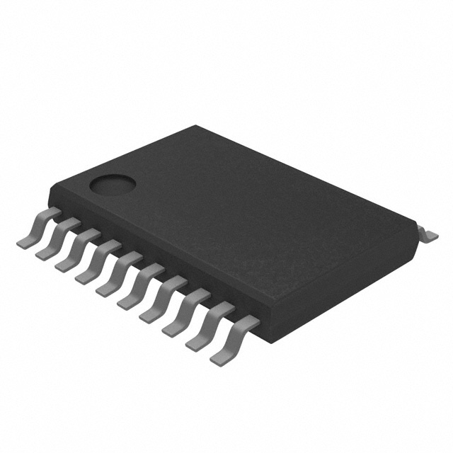
Available in a 20-Pin TSSOP (PW) package
Notebook PCs
Medical and Test Equipment
Portable Instrumentation
DESCRIPTION
The bq20z40 SBS-compliant gas gauge and
protection IC, incorporating patented Impedance
Track™ technology, is designed for battery-pack or
in-system installation. The bq20z40 measures and
maintains an accurate record of available charge in
Li-ion or Li-polymer batteries using its integrated
high-performance analog peripherals. The bq20z40
monitors capacity change, battery impedance,
open-circuit voltage, and other critical parameters of
the battery pack, and reports the information to the
system host controller over a serial-communication
bus. It is designed to work with the bq29330 analog
front-end (AFE) protection IC to maximizes
functionality and safety while minimizing external
component count and cost in smart battery circuits.
The Impedance Track™ technology continuously
analyzes the battery impedance, resulting in superior
gas-gauging accuracy. This enables the remaining
capacity to be calculated with discharge rate,
temperature, and cell aging that are all accounted for
during each stage of every cycle.
Table 1. AVAILABLE OPTIONS
TA
–40°C to 85°C
(1)
(2)
PACKAGE
20-PIN TSSOP (PW) Tube
20-PIN TSSOP (PW) Tape & Reel
bq20z40PW (1)
bq20z40PWR (2)
A single tube quantity is 50 units.
A single reel quantity is 2000 units
1
2
Please be aware that an important notice concerning availability, standard warranty, and use in critical applications of Texas
Instruments semiconductor products and disclaimers thereto appears at the end of this data sheet.
Impedance Track is a trademark of Texas Instruments.
PRODUCTION DATA information is current as of publication date.
Products conform to specifications per the terms of the Texas
Instruments standard warranty. Production processing does not
necessarily include testing of all parameters.
Copyright © 2009, Texas Instruments Incorporated
�Not Recommended for New Designs
bq20z40
SLUS801A – FEBRUARY 2009 – REVISED MARCH 2009
www.ti.com
These devices have limited built-in ESD protection. The leads should be shorted together or the device placed in conductive foam
during storage or handling to prevent electrostatic damage to the MOS gates.
SYSTEM PARTITIONING DIAGRAM
Pack +
Fuse
Supply Voltage
Reset
32KHz
SBS v1.1
Data
System
Interface
N-CH FET
Drive
Watchdog &
Protection
Timing
Charge Pumps
Registers
Alert
System
Interface
I2C
SHA-1
Authentication
Overvoltage &
Undervoltage
Protection
Cell & Pack
Voltage
Measurement
Voltage Level
Translator
Cell Balancing
Algorithm &
Control
Overrcurrent
Protection
Impedance
Track™ Gas
Gauging
Overcurrent &
Short Circuit
Protection
bq20z40
bq29330
nd
bq29330
Validation &
Control
SMBus
LDO
& Therm. Drive
& Reset
2 Level Voltage Protection
32kHz Clock
Generator
Therm
Cell Selection Multiplexer
Charging
Algorithm
Temperature
Measurement
& Protection
Cell Balancing Drive
Fail Safe
Protection
bq294xy
Pack RSNS
5mΩ – 20mΩ typ.
Figure 1.
2
Submit Documentation Feedback
Copyright © 2009, Texas Instruments Incorporated
Product Folder Link(s) :bq20z40
�Not Recommended for New Designs
bq20z40
www.ti.com
SLUS801A – FEBRUARY 2009 – REVISED MARCH 2009
TSSOP (PW)
(TOP VIEW)
XALERT
TS2
TS1
CLKOUT
PRES
PFIN
SAFE
SMBD
NC
SMBC
1
2
3
4
5
6
7
8
9
10
20
19
18
17
16
15
14
13
12
11
VCELLVCELL+
VCC
VSS
MRST
SRN
SRP
VSS
SCLK
SDATA
PIN FUNCTIONS
PIN
I/O (1)
DESCRIPTION
NO.
NAME
1
XALERT
I
Input from bq29330 XALERT output.
2
TS2
I
2nd Thermistor voltage input connection to monitor temperature
3
TS1
I
1st Thermistor voltage input connection to monitor temperature
4
CLKOUT
O
32.768-kHz output for the bq29330. This pin should be directly connected to the AFE.
5
PRES
I
Active low input to sense system insertion. Typically requires additional ESD protection.
6
PFIN
I
Active low input to detect secondary protector output status, and to allow the bq20z40 to report the
status of the 2nd level protection output
Active high output to enforce additional level of safety protection; e.g., fuse blow.
7
SAFE
O
8
SMBD
I/OD
9
NC
–
10
SMBC
I/OD
11
SDATA
I/O
Data transfer to and from bq29330
12
SCLK
I/O
Communication clock to the bq29330
13
VSS
–
Connected I/O pin to VSS
14
SRP
IA
Connections for a small-value sense resistor to monitor the battery charge- and discharge-current
flow
15
SRN
IA
Connections for a small-value sense resistor to monitor the battery charge- and discharge-current
flow
16
MRST
I
Master reset input that forces the device into reset when held low. Must be held high for normal
operation
17
VSS
P
Negative Supply Voltage
18
VCC
P
Positive Supply Voltage
19
VCELL+
I
Input from bq29330 used to read a scaled value of individual cell voltages
20
VCELL–
I
Input from bq29330 used to read a scaled value of individual cell voltages
(1)
SMBus data open-drain bidirectional pin used to transfer address and data to and from the bq20z40
Not used— leave floating
SMBus clock open-drain bidirectional pin used to clock the data transfer to and from the bq20z40
I = Input, IA = Analog input, I/O = Input/output, I/OD = Input/Open-drain output, O = Output, OA = Analog output, P = Power
ABSOLUTE MAXIMUM RATINGS
over operating free-air temperature range (unless otherwise noted) (1)
RANGE
VCC relative to VSS
Supply voltage range
V(IOD) relative to VSS
Open-drain I/O pins
VI relative to VSS
Input voltage range to all other pins
TA
Operating free-air temperature range
–40°C to 85°C
Tstg
Storage temperature range
–65°C to 150°C
(1)
–0.3 V to 2.75 V
–0.3 V to 6 V
–0.3 V to VCC + 0.3 V
Stresses beyond those listed under absolute maximum ratings may cause permanent damage to the device. These are stress ratings
only, and functional operation of the device at these or any other conditions beyond those indicated under recommended operating
conditions is not implied. Exposure to absolute-maximum-rated conditions for extended periods may affect device reliability.
Submit Documentation Feedback
Copyright © 2009, Texas Instruments Incorporated
Product Folder Link(s) :bq20z40
3
�Not Recommended for New Designs
bq20z40
SLUS801A – FEBRUARY 2009 – REVISED MARCH 2009
www.ti.com
ELECTRICAL CHARACTERISTICS
VCC = 2.4 V to 2.6 V, TA = –40°C to 85°C (unless otherwise noted)
PARAMETER
VCC
TEST CONDITIONS
Supply voltage
MIN
TYP
MAX
2.4
2.5
2.6
400 (1)
No flash programming
UNIT
V
ICC
Operating mode current
I(SLP)
Low-power storage mode current
I(SD)
Shutdown Mode Current
VOL
Output voltage low SMBC, SMBD, SDATA, SCLK, SAFE
VOH
Output high voltage, SMBC, SMBD, SDATA, SCLK, SAFE IOH = –1 mA
VIL
Input voltage low SMBC, SMBD, SDATA, SCLK,
XALERT, PRES, PFIN
VIH
Input voltage high SMBC, SMBD, SDATA, SCLK,
XALERT, PRES, PFIN
CIN
Input capacitance
V(AI1)
Input voltage range VCELL+, VCELL-,TS1, TS2
V(AI2)
Input voltage range SRN, SRP
Z(AI2)
Input impedance VCELL+, VCELL-, TS1, TS2
0 V–1 V
8
MΩ
Z(AI1)
Input impedance SRN, SRP
0 V–1 V
2.5
MΩ
(1)
bq20z40 + bq29330
475
Sleep mode
8 (1)
bq20z40 + bq29330
mA
mA
51
0.1 (1)
Shutdown mode
bq20z40 + bq29330
mA
0.2
IOL = 0.5 mA
0.4
VCC – 0.5
V
V
–0.3
0.8
V
2
6
V
5
pF
–0.2
0.8xVCC
– 0.20
0.20
V
This value does not include the bq29330
POWER-ON RESET
VCC = 2.4V to 2.6 V, TA = –40°C to 85°C (unless otherwise noted)
MIN
TYP
MAX
VIT–
Negative-going voltage input
PARAMETER
TEST CONDITIONS
1.7
1.8
1.9
UNIT
V
VHYS
Power-on reset hysteresis
50
125
200
mV
POWER ON RESET BEHAVIOR
VS
FREE-AIR TEMPERATURE
Power-On Reset Negative-Going Voltage - V
1.81
1.8
1.79
1.78
1.77
1.76
-40
-20
0
20
40
60
80
TA - Free-Air Temperature - °C
INTEGRATING ADC (Coulomb Counter) CHARACTERISTICS
VCC = 2.4V to 2.6 V, TA = –40°C to 85°C (unless otherwise noted)
4
Submit Documentation Feedback
Copyright © 2009, Texas Instruments Incorporated
Product Folder Link(s) :bq20z40
�Not Recommended for New Designs
bq20z40
www.ti.com
SLUS801A – FEBRUARY 2009 – REVISED MARCH 2009
INTEGRATING ADC (Coulomb Counter) CHARACTERISTICS (continued)
VCC = 2.4V to 2.6 V, TA = –40°C to 85°C (unless otherwise noted)
PARAMETER
V(SR)
Input voltage range, V(SRN) and V(SRP)
V(SROS)
Input offset
INL
Integral nonlinearity error
TEST CONDITIONS
MIN
V(SR) = V(SRN) – V(SRP)
TYP
MAX
–0.2
0.2
10
UNIT
V
mV
0.007%
0.034%
OSCILLATOR
VCC = 2.4 V to 2.6 V, TA = –40°C to 85°C (unless otherwise noted)
PARAMETER
TEST CONDITIONS
MIN
TYP
MAX
UNIT
4.194
MHz
HIGH FREQUENCY OSCILLATOR
f(OSC) Operating Frequency
f(EIO) Frequency Error (1)
(2)
TA = 20°C to 70°C
–3% 0.25%
3%
–2% 0.25%
2%
2.5
5
t(SXO) Start-up Time (3)
ms
LOW FREQUENCY OSCILLATOR
f(LOSC) Operating Frequency
f(LEIO) Frequency Error (2)
t(LSXO) Start-up time
(1)
(2)
(3)
(4)
(5)
32.768
(4)
TA = 20°C to 70°C
KHz
–2.5% 0.25%
2.5%
–1.5% 0.25%
1.5%
(5)
500
ms
The frequency error is measured from 4.194 MHz.
The frequency drift is included and measured from the trimmed frequency at VCC = 2.5 V, TA = 25°C.
The start-up time is defined as the time it takes for the oscillator output frequency to be within 1 % of the specified frequency.
The frequency error is measured from 32.768 kHz.
The start-up time is defined as the time it takes for the oscillator output frequency to be ± 3%.
DATA FLASH MEMORY CHARACTERISTICS
VCC = 2.4 V to 2.6 V, TA = –40°C to 85°C (unless otherwise noted)
PARAMETER
tDR
TEST CONDITIONS
See
(1)
10
Flash programming write-cycles
See
(1)
20,000
See
(1)
See
(1)
t(WORDPROG) Word programming time
I(DDdPROG)
(1)
MIN
Data retention
Flash-write supply current
TYP
MAX
UNIT
Years
Cycles
2
ms
5
10
mA
TYP
MAX
Specified by design. Not production tested.
SMBus TIMING SPECIFICATIONS
VCC = 2.4 V to 2.6 V, TA = –40°C to 85°C (unless otherwise noted)
PARAMETER
TEST CONDITIONS
MIN
fSMB
SMBus operating frequency
Slave mode, SMBC 50% duty cycle
fMAS
SMBus master clock frequency
Master mode, no clock low slave extend
tBUF
Bus free time between start and stop
tHD:STA
Hold time after (repeated) start
tSU:STA
Repeated start setup time
tSU:STO
Stop setup time
tHD:DAT
Data hold time
tSU:DAT
Data setup time
tTIMEOUT
Error signal/detect
(1)
10
100
51.2
UNIT
kHz
4.7
4
ms
4.7
4
Receive mode
0
Transmit mode
300
ns
250
See
(1)
25
35
ms
The bq20z40 times out when any clock low exceeds tTIMEOUT.
Submit Documentation Feedback
Copyright © 2009, Texas Instruments Incorporated
Product Folder Link(s) :bq20z40
5
�Not Recommended for New Designs
bq20z40
SLUS801A – FEBRUARY 2009 – REVISED MARCH 2009
www.ti.com
SMBus TIMING SPECIFICATIONS (continued)
VCC = 2.4 V to 2.6 V, TA = –40°C to 85°C (unless otherwise noted)
PARAMETER
TEST CONDITIONS
MIN
TYP
MAX
tLOW
Clock low period
tHIGH
Clock high period
See
(2)
tLOW:SEXT
Cumulative clock low slave extend time
See
(3)
25
tLOW:MEXT
Cumulative clock low master extend time
See
(4)
10
tF
Clock/data fall time
(VILMAX – 0.15 V) to (VIHMIN + 0.15 V)
tR
Clock/data rise time
0.9 VCC to (VILMAX – 0.15 V)
(2)
(3)
(4)
4.7
4
50
300
1000
UNIT
ms
ms
ns
tHIGH:MAX. is minimum bus idle time. SMBC = 1 for t > 50 ms causes reset of any transaction involving the bq20z40 that is in progress.
tLOW:SEXT is the cumulative time a slave device is allowed to extend the clock cycles in one message from initial start to the stop.
tLOW:MEXT is the cumulative time a master device is allowed to extend the clock cycles in one message from initial start to the stop.
SMBus TIMING DIAGRAM
t LOW
SCLK
tR
t HD:STA
tF
t HD:STA
t SU:STA
t HIGH
t SU:STO
t SU:DAT
t HD:DAT
SDATA
t BUF
P
S
S
Start
P
Stop
t LOW:SEXT
SCLK ACK
t LOW:MEXT
SCLK ACK
t LOW:MEXT
t LOW:MEXT
SCLK
SDATA
6
Submit Documentation Feedback
Copyright © 2009, Texas Instruments Incorporated
Product Folder Link(s) :bq20z40
�Not Recommended for New Designs
bq20z40
www.ti.com
SLUS801A – FEBRUARY 2009 – REVISED MARCH 2009
FEATURE SET
Primary (1st Level) Safety Features
The bq20z40 supports a wide range of battery and system protection features that can easily be configured. The
primary safety features include:
•
•
•
•
•
Cell over/undervoltage protection
Charge and discharge overcurrent
Short Circuit
Charge and discharge overtemperature with independent alarms and thresholds for each thermistor
AFE Watchdog
Secondary (2nd Level) Safety Features
The secondary safety features of the bq20z40 can be used to indicate more serious faults via the SAFE (pin 7).
This pin can be used to blow an in-line fuse to permanently disable the battery pack from charging or
discharging. The secondary safety protection features include:
•
•
•
•
•
•
•
•
•
Safety overvoltage
Safety undervoltage
Safety overcurrent in charge and discharge
Safety overtemperature in charge and discharge with independent alarms and thresholds for each thermistor
Charge FET and 0 Volt Charge FET fault
Discharge FET fault
Cell imbalance detection (active and at rest)
Open thermistor detection
AFE communication fault
Charge Control Features
The bq20z40 charge control features include:
• Supports JEITA temperature ranges. Reports charging voltage and charging current according to the
active temperature range.
• Handles more complex charging profiles. Allows for splitting the standard temperature range into 2
sub-ranges and allows for varying the charging current according to the cell voltage.
• Reports the appropriate charging current needed for constant current charging and the appropriate
charging voltage needed for constant voltage charging to a smart charger using SMBus broadcasts.
• Determines the chemical state of charge of each battery cell using Impedance Track™ and can reduce
the charge difference of the battery cells in fully charged state of the battery pack gradually using cell
balancing algorithm during charging. This prevents fully charged cells from overcharging and causing
excessive degradation and also increases the usable pack energy by preventing premature charge
termination
• Supports pre-charging/zero-volt charging
• Supports charge inhibit and charge suspend if battery pack temperature is out of temperature range
• Reports charging fault and also indicate charge status via charge and discharge alarms.
Gas Gauging
The bq20z40 uses the Impedance Track™ Technology to measure and calculate the available charge in battery
cells. The achievable accuracy is better than 1% error over the lifetime of the battery and there is no full charge
discharge learning cycle required.
See Theory and Implementation of Impedance Track Battery Fuel-Gauging Algorithm application note (SLUA364)
for further details.
Submit Documentation Feedback
Copyright © 2009, Texas Instruments Incorporated
Product Folder Link(s) :bq20z40
7
�Not Recommended for New Designs
bq20z40
SLUS801A – FEBRUARY 2009 – REVISED MARCH 2009
www.ti.com
Lifetime Data Logging Features
The bq20z40 offers lifetime data logging, where important measurements are stored for warranty and analysis
purposes. The data monitored include:
• Lifetime maximum temperature
• Lifetime minimum temperature
• Lifetime maximum battery cell voltage
• Lifetime minimum battery cell voltage
• Lifetime maximum battery pack voltage
• Lifetime minimum battery pack voltage
• Lifetime maximum charge current
• Lifetime maximum discharge current
• Lifetime maximum charge power
• Lifetime maximum discharge power
• Lifetime maximum average discharge current
• Lifetime maximum average discharge power
• Lifetime average temperature
Authentication
The bq20z40 supports authentication by the host using SHA-1.
Power Modes
The bq20z40 supports 3 different power modes to reduce power consumption:
•
•
•
In Normal Mode, the bq20z40 performs measurements, calculations, protection decisions and data updates in
1 second intervals. Between these intervals, the bq20z40 is in a reduced power stage.
In Sleep Mode, the bq20z40 performs measurements, calculations, protection decisions and data update in
adjustable time intervals. Between these intervals, the bq20z40 is in a reduced power stage. The bq20z40
has a wake function that enables exit from Sleep mode, when current flow or failure is detected.
In Shutdown Mode the bq20z40 is completely disabled.
CONFIGURATION
Oscillator Function
The bq20z40 fully integrates the system and processor oscillators and, therefore, requires no pins or
components for this feature.
System Present Operation
The bq20z40 periodically verifies the PRES pin and detects that the battery is present in the system via a low
state on a PRES input. When this occurs, bq20z40 enters normal operating mode. When the pack is removed
from the system and the PRES input is high, the bq20z40 enters the battery-removed state, disabling the charge,
discharge and ZVCHG FETs. The PRES input is ignored and can be left floating when non-removal mode is set
in the data flash.
BATTERY PARAMETER MEASUREMENTS
The bq20z40 uses an integrating delta-sigma analog-to-digital converter (ADC) for current measurement, and a
second delta-sigma ADC for individual cell and battery voltage, and temperature measurement.
8
Submit Documentation Feedback
Copyright © 2009, Texas Instruments Incorporated
Product Folder Link(s) :bq20z40
�Not Recommended for New Designs
bq20z40
www.ti.com
SLUS801A – FEBRUARY 2009 – REVISED MARCH 2009
Charge and Discharge Counting
The integrating delta-sigma ADC measures the charge/discharge flow of the battery by measuring the voltage
drop across a small-value sense resistor between the SRP and SRN pins. The integrating ADC measures bipolar
signals from -0.25 V to 0.25 V. The bq20z40 detects charge activity when VSR = V(SRP) - V(SRN) is positive, and
discharge activity when VSR = V(SRP) - V(SRN) is negative. The bq20z40 continuously integrates the signal over
time, using an internal counter. The fundamental rate of the counter is 0.65 nVh.
Voltage
The bq20z40 updates the individual series cell voltages through the bq29330 at one second intervals. The
bq20z40 configures the bq29330 to connect the selected cell, cell offset, or bq29330 VREF to the CELL pin of
the bq29330, which is required to be connected to VIN of the bq20z40. The internal ADC of the bq20z40
measures the voltage, scales it, and calibrates itself appropriately. This data is also used to calculate the
impedance of the cell for the Impedance Track™ gas-gauging.
Current
The bq20z40 uses the SRP and SRN inputs to measure and calculate the battery charge and discharge current
using a 5 mΩ to 20 mΩ typ. sense resistor.
Wake Function
The bq20z40 can exit sleep mode, if enabled, by the presence of a programmable level of current signal across
SRP and SRN.
Auto Calibration
The bq20z40 provides an auto-calibration feature to cancel the voltage offset error across SRP and SRN for
maximum charge measurement accuracy. The bq20z40 performs auto-calibration when the SMBus lines stay
low continuously for a minimum of a programmable amount of time.
Temperature
The bq20z40 has an internal temperature sensor and inputs for 2 external temperature sensors, TS1 and TS2,
used in conjunction with two identical NTC thermistors (default are Semitec 103AT) to sense the battery
environmental temperature. The bq20z40 can be configured to use internal, or up to 2 external temperature
sensors.
COMMUNICATIONS
The bq20z40 uses SMBus v1.1 with Master Mode and package error checking (PEC) options per the SBS
specification.
SMBus On and Off State
The bq20z40 detects an SMBus off state when SMBC and SMBD are logic-low for ≥ 2 seconds. Clearing this
state requires either SMBC or SMBD to transition high. Within 1 ms, the communication bus is available.
Submit Documentation Feedback
Copyright © 2009, Texas Instruments Incorporated
Product Folder Link(s) :bq20z40
9
�Not Recommended for New Designs
bq20z40
SLUS801A – FEBRUARY 2009 – REVISED MARCH 2009
www.ti.com
SBS Commands
Table 2. SBS COMMANDS
SBS Cmd
Mode
Name
Format
Size in
Bytes
Min
Value
Max
Value
Default Value
0x00
R/W
ManufacturerAccess
hex
2
0x0000
0xffff
—
0x01
R/W
RemainingCapacityAlarm
unsigned int
2
0
65535
300
mAh or
10mWh
0x02
R/W
RemainingTimeAlarm
unsigned int
2
0
65535
10
min
0x03
R/W
BatteryMode
hex
2
0x0000
0xe383
—
0x04
R/W
AtRate
signed int
2
-32768
32767
—
mA or 10mW
0x05
R
AtRateTimeToFull
unsigned int
2
0
65534
—
min
0x06
R
AtRateTimeToEmpty
unsigned int
2
0
65534
—
min
0x07
R
AtRateOK
unsigned int
2
0
65535
—
0x08
R
Temperature
unsigned int
2
0
65535
—
0.1°K
0x09
R
Voltage
unsigned int
2
0
65535
—
mV
0x0a
R
Current
signed int
2
-32768
32767
—
mA
0x0b
R
AverageCurrent
signed int
2
-32768
32767
—
mA
0x0c
R
MaxError
unsigned int
1
0
100
—
%
0x0d
R
RelativeStateOfCharge
unsigned int
1
0
100
—
%
0x0e
R
AbsoluteStateOfCharge
unsigned int
1
0
100+
—
%
0x0f
R/W
RemainingCapacity
unsigned int
2
0
65535
—
mAh or
10mWh
0x10
R
FullChargeCapacity
unsigned int
2
0
65535
—
mAh or
10mWh
0x11
R
RunTimeToEmpty
unsigned int
2
0
65534
—
min
0x12
R
AverageTimeToEmpty
unsigned int
2
0
65534
—
min
0x13
R
AverageTimeToFull
unsigned int
2
0
65534
—
min
0x14
R
ChargingCurrent
unsigned int
2
0
65534
—
mA
0x15
R
ChargingVoltage
unsigned int
2
0
65534
—
mV
0x16
R
BatteryStatus
hex
2
0x0000
0xdbff
—
0x17
R/W
CycleCount
unsigned int
2
0
65535
—
0x18
R/W
DesignCapacity
unsigned int
2
0
65535
4400
mAh or
10mWh
0x19
R/W
DesignVoltage
unsigned int
2
0
65535
14400
mV
0x1a
R/W
SpecificationInfo
hex
2
0x0000
0xffff
0x0031
0x1b
R/W
ManufactureDate
unsigned int
2
—
—
01-Jan-1980
0x1c
R/W
SerialNumber
hex
2
0x0000
0xffff
0x0001
0x20
R/W
ManufacturerName
String
20+1
—
—
Texas Inst.
—
0x21
R/W
DeviceName
String
20+1
—
—
bq20z40
—
0x22
R/W
DeviceChemistry
String
4+1
—
—
LION
—
0x23
R/W
ManufacturerData
String
14+1
—
—
—
—
0x2f
R/W
Authenticate
String
20+1
—
—
—
—
0x3c
R
CellVoltage4
unsigned int
2
0
65535
—
mV
0x3d
R
CellVoltage3
unsigned int
2
0
65535
—
mV
0x3e
R
CellVoltage2
unsigned int
2
0
65535
—
mV
0x3f
R
CellVoltage1
unsigned int
2
0
65535
—
mV
10
Submit Documentation Feedback
Unit
—
Copyright © 2009, Texas Instruments Incorporated
Product Folder Link(s) :bq20z40
�Not Recommended for New Designs
bq20z40
www.ti.com
SLUS801A – FEBRUARY 2009 – REVISED MARCH 2009
Table 3. EXTENDED SBS COMMANDS
SBS
Cmd
Mode
Name
Format
Size in
Bytes
Min Value
Max Value
Default
Value
Unit
0x45
R
AFEData
String
11+1
—
—
—
—
0x46
R/W
FETControl
hex
2
0x00
0xff
—
—
0x4f
R
StateOfHealth
hex
2
0x0000
0xffff
—
%
0x51
R
SafetyStatus
hex
2
0x0000
0xffff
—
—
0x53
R
PFStatus
hex
2
0x0000
0xffff
—
—
0x54
R
OperationStatus
hex
2
0x0000
0xffff
—
—
0x55
R
ChargingStatus
hex
2
0x0000
0xffff
—
—
0x57
R
ResetData
hex
2
0x0000
0xffff
—
—
0x58
R
WDResetData
unsigned int
2
0
65535
—
—
0x5a
R
PackVoltage
unsigned int
2
0
65535
—
mV
0x5d
R
AverageVoltage
unsigned int
2
0
65535
—
mV
0x5e
R
TS1Temperature
integer
2
–400
1200
—
0.1°C
0x5f
R
TS2Temperature
integer
2
–400
1200
—
0.1°C
0x60
R/W
UnSealKey
hex
4
0x00000000
0xffffffff
—
—
0x61
R/W
FullAccessKey
hex
4
0x00000000
0xffffffff
—
—
0x62
R/W
PFKey
hex
4
0x00000000
0xffffffff
—
—
0x63
R/W
AuthenKey3
hex
4
0x00000000
0xffffffff
—
—
0x64
R/W
AuthenKey2
hex
4
0x00000000
0xffffffff
—
—
0x65
R/W
AuthenKey1
hex
4
0x00000000
0xffffffff
—
—
0x66
R/W
AuthenKey0
hex
4
0x00000000
0xffffffff
—
—
0x69
R
SafetyStatus2
hex
2
0x0000
0x0003
—
—
0x6b
R
PFStatus2
hex
2
0x0000
0x0003
—
—
0x6c
R/W
ManufBlock1
String
20
—
—
—
—
0x6d
R/W
ManufBlock2
String
20
—
—
—
—
0x6e
R/W
ManufBlock3
String
20
—
—
—
—
0x6f
R/W
ManufBlock4
String
20
—
—
—
—
0x70
R/W
ManufacturerInfo
String
31+1
—
—
—
—
0x71
R/W
SenseResistor
unsigned int
2
0
65535
—
mΩ
0x72
R
TempRange
hex
2
—
—
—
—
0x73
R
LifetimeData
String
32+1
—
—
—
—
0x77
R/W
DataFlashSubClassID
hex
2
0x0000
0xffff
—
—
0x78
R/W
DataFlashSubClassPage1
hex
32
—
—
—
—
0x79
R/W
DataFlashSubClassPage2
hex
32
—
—
—
—
0x7a
R/W
DataFlashSubClassPage3
hex
32
—
—
—
—
0x7b
R/W
DataFlashSubClassPage4
hex
32
—
—
—
—
0x7c
R/W
DataFlashSubClassPage5
hex
32
—
—
—
—
0x7d
R/W
DataFlashSubClassPage6
hex
32
—
—
—
—
0x7e
R/W
DataFlashSubClassPage7
hex
32
—
—
—
—
0x7f
R/W
DataFlashSubClassPage8
hex
32
—
—
—
—
Submit Documentation Feedback
Copyright © 2009, Texas Instruments Incorporated
Product Folder Link(s) :bq20z40
11
�Not Recommended for New Designs
bq20z40
SLUS801A – FEBRUARY 2009 – REVISED MARCH 2009
www.ti.com
APPLICATION SCHEMATIC
12
Submit Documentation Feedback
Copyright © 2009, Texas Instruments Incorporated
Product Folder Link(s) :bq20z40
�PACKAGE OPTION ADDENDUM
www.ti.com
10-Dec-2020
PACKAGING INFORMATION
Orderable Device
Status
(1)
Package Type Package Pins Package
Drawing
Qty
Eco Plan
(2)
Lead finish/
Ball material
MSL Peak Temp
Op Temp (°C)
Device Marking
(3)
(4/5)
(6)
BQ20Z40PW
NRND
TSSOP
PW
20
70
RoHS & Green
NIPDAU
Level-1-260C-UNLIM
-40 to 85
20Z40
BQ20Z40PWR
NRND
TSSOP
PW
20
2000
RoHS & Green
NIPDAU
Level-1-260C-UNLIM
-40 to 85
20Z40
(1)
The marketing status values are defined as follows:
ACTIVE: Product device recommended for new designs.
LIFEBUY: TI has announced that the device will be discontinued, and a lifetime-buy period is in effect.
NRND: Not recommended for new designs. Device is in production to support existing customers, but TI does not recommend using this part in a new design.
PREVIEW: Device has been announced but is not in production. Samples may or may not be available.
OBSOLETE: TI has discontinued the production of the device.
(2)
RoHS: TI defines "RoHS" to mean semiconductor products that are compliant with the current EU RoHS requirements for all 10 RoHS substances, including the requirement that RoHS substance
do not exceed 0.1% by weight in homogeneous materials. Where designed to be soldered at high temperatures, "RoHS" products are suitable for use in specified lead-free processes. TI may
reference these types of products as "Pb-Free".
RoHS Exempt: TI defines "RoHS Exempt" to mean products that contain lead but are compliant with EU RoHS pursuant to a specific EU RoHS exemption.
Green: TI defines "Green" to mean the content of Chlorine (Cl) and Bromine (Br) based flame retardants meet JS709B low halogen requirements of