bq20z655
www.ti.com
SLUSAH8A – APRIL 2011 – REVISED MAY 2012
SBS 1.1-COMPLIANT GAS GAUGE AND PROTECTION
ENABLED WITH IMPEDANCE TRACK™
Check for Samples: bq20z655
FEATURES
APPLICATIONS
•
•
•
•
•
1
2
•
•
•
•
•
•
•
•
•
•
•
•
Next Generation Patented Impedance Track™
Technology Accurately Measures Available
Charge in Li-Ion and Li-Polymer Batteries
– Better Than 1% Error Over the Lifetime of
the Battery
Supports the Smart Battery Specification
SBS V1.1
Flexible Configuration for 2-Series to 4-Series
Li-Ion and Li-Polymer Cells
Powerful 8-Bit RISC CPU with Ultralow Power
Modes
Charge Enable (CE) Affects the Normal
Operation on the Charge FET when the Battery
Is in Charge/Relax Mode
Full Array of Programmable Protection
Features
– Voltage, Current, and Temperature
Satisfies JEITA Guidelines
Added Flexibility to Handle More Complex
Charging Profiles
Lifetime Data Logging
Drives 3, 4, or 5 Segment Liquid Crystal
Display and LED for Battery-Pack Conditions
Supports SHA-1 Authentication
Complete Battery Protection and Gas Gauge
Solution in One Package
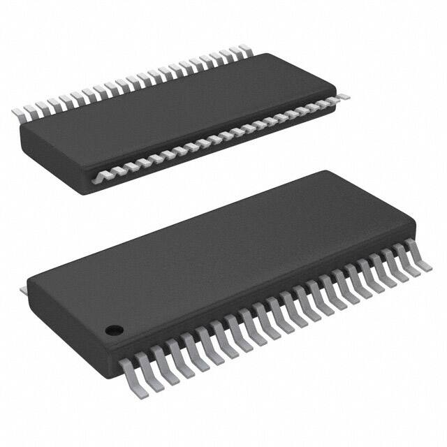
Available in a 44-Pin TSSOP (DBT) Package
Medical and Test Equipment
Portable Instrumentation
Rechargeable Battery Packs
Industrial Equipment
DESCRIPTION
The bq20z655 SBS-compliant gas gauge and
protection IC, incorporating patented Impedance
Track™ technology, is a single IC solution designed
for battery-pack or in-system installation. The
bq20z655 measures and maintains an accurate
record of available charge in Li-Ion or Li-Polymer
batteries using its integrated high-performance
analog peripherals. The bq20z655 monitors capacity
change, battery impedance, open-circuit voltage, and
other critical parameters of the battery pack which
reports the information to the system host controller
over a serial-communication bus. Together with the
integrated analog front-end (AFE) short-circuit and
overload protection, the bq20z655 maximizes
functionality and safety while minimizing external
component count, cost, and size in smart battery
circuits.
The implemented Impedance Track™ gas gauging
technology continuously analyzes the battery
impedance, resulting in superior gas-gauging
accuracy. This enables remaining capacity to be
calculated with discharge rate, temperature, and cell
aging all accounted for during each stage of every
cycle with high accuracy.
Table 1. AVAILABLE OPTIONS
TA
–40°C to 85°C
(1)
(2)
(3)
PACKAGE (1)
44-PIN TSSOP (DBT) Tube
bq20z655DBT
(2)
44-PIN TSSOP (DBT) Tape and Reel
bq20z655DBTR (3)
For the most current package and ordering information, see the Package Option Addendum at the end of this document, or see the TI
website at www.ti.com.
A single tube quantity is 40 units.
A single reel quantity is 2000 units.
1
2
Please be aware that an important notice concerning availability, standard warranty, and use in critical applications of
Texas Instruments semiconductor products and disclaimers thereto appears at the end of this data sheet.
Impedance Track is a trademark of Texas Instruments.
PRODUCTION DATA information is current as of publication date.
Products conform to specifications per the terms of the Texas
Instruments standard warranty. Production processing does not
necessarily include testing of all parameters.
Copyright © 2011–2012, Texas Instruments Incorporated
�bq20z655
SLUSAH8A – APRIL 2011 – REVISED MAY 2012
www.ti.com
This integrated circuit can be damaged by ESD. Texas Instruments recommends that all integrated circuits be handled with
appropriate precautions. Failure to observe proper handling and installation procedures can cause damage.
ESD damage can range from subtle performance degradation to complete device failure. Precision integrated circuits may be more
susceptible to damage because very small parametric changes could cause the device not to meet its published specifications.
PACKAGE THERMAL DATA
THERMAL INFORMATION
bq20z655
THERMAL METRIC (1)
TSSOP
UNITS
44 PINS
θJA, High K
Junction-to-ambient thermal resistance (2)
θJC(top)
Junction-to-case(top) thermal resistance
θJB
Junction-to-board thermal resistance
60.9
(3)
15.3
(4)
30.2
(5)
ψJT
Junction-to-top characterization parameter
ψJB
Junction-to-board characterization parameter
θJC(bottom)
(1)
(2)
(3)
(4)
(5)
(6)
(7)
Junction-to-case(bottom) thermal resistance
°C/W
0.3
(6)
27.2
(7)
n/a
For more information about traditional and new thermal metrics, see the IC Package Thermal Metrics application report, SPRA953.
The junction-to-ambient thermal resistance under natural convection is obtained in a simulation on a JEDEC-standard, high-K board, as
specified in JESD51-7, in an environment described in JESD51-2a.
The junction-to-case (top) thermal resistance is obtained by simulating a cold plate test on the package top. No specific JEDECstandard test exists, but a close description can be found in the ANSI SEMI standard G30-88.
The junction-to-board thermal resistance is obtained by simulating in an environment with a ring cold plate fixture to control the PCB
temperature, as described in JESD51-8.
The junction-to-top characterization parameter, ψJT, estimates the junction temperature of a device in a real system and is extracted
from the simulation data for obtaining θJA, using a procedure described in JESD51-2a (sections 6 and 7).
The junction-to-board characterization parameter, ψJB, estimates the junction temperature of a device in a real system and is extracted
from the simulation data for obtaining θJA , using a procedure described in JESD51-2a (sections 6 and 7).
The junction-to-case (bottom) thermal resistance is obtained by simulating a cold plate test on the exposed (power) pad. No specific
JEDEC standard test exists, but a close description can be found in the ANSI SEMI standard G30-88.
SYSTEM PARTITIONING DIAGRAM
VSS
VCC
BAT
PACK
PRES
CHG
DSG
ZVCHG
GPOD
PMS
SAFE
PFIN
LED5
LED3
LED4
LED1
LED2
PACK+
RBI
DISP
LED Display
Fuse Blow
Detection & Logic
PreCharge FET
& GPOD Drive
Oscillator
N Channel FET
Drive
Power Mode
Control
MSRT
RESET
SMBD
SMB 1.1
System Control
AFE HW Control
Watchdog
ALERT
SMBC
Voltage
Measurement
Data Flash
Memory
Cell Voltage
Multiplexer
VCELL+
+
VC1
VC2
JEITA and
Enhanced
Charging
Algorithm
Over
Temperature
Protection
SHA-1
Authentication
Temperature
Measurement
Over & Under
Voltage
Protection
VC3
Impedance
Track™ Gas
Gauging
Cell Balancing
VC4
+
+
+
VC1
VDD
VC2
OUT
VC3
CD
VC4
GND
bq294xx
VC5
Over Current
Protection
HW Over
Current & Short
Circuit Protection
Coulomb
Counter
REG33
Regulators
PACK–
2
ASRN
ASRP
GSRP
GSRN
TS2
TS1
TOUT
REG25
RSNS
5 mΩ – 20 mΩ typ
Submit Documentation Feedback
Copyright © 2011–2012, Texas Instruments Incorporated
Product Folder Link(s): bq20z655
�bq20z655
www.ti.com
SLUSAH8A – APRIL 2011 – REVISED MAY 2012
PACKAGE PINOUT DIAGRAM
bq20z655
DBT PACKAGE
(TOP VIEW)
DSG
1
44
CHG
PACK
2
43
BAT
VCC
3
42
VC1
ZVCHG
4
41
VC2
GPOD/ALARM
5
40
VC3
PMS
6
39
VC4
VSS
7
38
VC5
REG33
8
37
ASRP
TOUT
9
36
ASRN
VCELL+
10
35
RESET
¯¯¯¯¯¯
¯¯¯¯¯¯
ALERT
11
34
VSS
COM
12
33
RBI
TS1
13
32
REG25
TS2
14
31
VSS
PRES
¯¯¯¯¯
15
30
MRST
¯¯¯¯¯
PFIN
¯¯¯¯
16
29
GSRN
SAFE
17
28
GSRP
SMBD
18
27
LED5/SEG5
CE
19
26
LED4/SEG4
SMBC
20
25
LED3/SEG3
¯¯¯¯
DISP
21
24
LED2/SEG2
22
23
LED1/SEG1
VSS
Figure 1. Package Pinout
Submit Documentation Feedback
Copyright © 2011–2012, Texas Instruments Incorporated
Product Folder Link(s): bq20z655
3
�bq20z655
SLUSAH8A – APRIL 2011 – REVISED MAY 2012
www.ti.com
TYPICAL LCD IMPLEMENTATION
Figure 2 shows a typical LCD implementation.
bq20z655
27
25
24
23
12
S5
SEG4
S4
SEG3
S3
SEG2
S2
SEG1
LCD 5 Seg Display
26
SEG5
S1 BP
COM
330 KΩ
(x6)
8
21
REG33
220 KΩ
DSPL
0.1 µF
Figure 2. Typical LCD Implementation
4
Submit Documentation Feedback
Copyright © 2011–2012, Texas Instruments Incorporated
Product Folder Link(s): bq20z655
�bq20z655
www.ti.com
SLUSAH8A – APRIL 2011 – REVISED MAY 2012
TERMINAL FUNCTIONS
TERMINAL
(1)
I/O (1)
DESCRIPTION
NO.
NAME
1
DSG
O
2
PACK
IA, P
3
VCC
P
Positive device supply input. Connect to the center connection of the CHG FET and DSG FET to
ensure device supply either from battery stack or battery pack input.
4
ZVCHG
O
P-chan pre-charge FET gate drive
5
GPOD
OD
6
PMS
I
High side N-chan discharge FET gate drive
Battery pack input voltage sense input. It also serves as device wake up when device is in shutdown
mode.
High voltage general purpose open drain output. It can be configured to be used in pre-charge
condition.
Pre-charge mode setting input. Connect to PACK to enable 0v pre-charge using charge FET
connected at CHG pin. Connect to VSS to disable 0-V pre-charge using charge FET connected at
CHG pin.
7
VSS
P
Negative supply voltage input. Connect all VSS pins together for operation of device.
8
REG33
P
3.3-V regulator output. Connect at least a 2.2-μF capacitor to REG33 and VSS.
9
TOUT
P
Thermistor bias supply output
10
VCELL+
—
Internal cell voltage multiplexer and amplifier output. Connect a 0.1-μF capacitor to VCELL+ and
VSS.
11
ALERT
OD
Alert output. In case of short circuit condition, overload condition, and watchdog time out, this pin will
be triggered.
12
COM/TP
—
Output/open drain: LCD common connection
13
TS1
IA
1st Thermistor voltage input connection to monitor temperature
14
TS2
IA
2nd Thermistor voltage input connection to monitor temperature
15
PRES
I
Active low input to sense system insertion. Typically requires additional ESD protection.
16
PFIN
I
Active low input to detect secondary protector status, and to allow the bq20z655 to report the status
of the 2nd level protection input
17
SAFE
OD
Active high output to enforce additional level of safety protection; e.g., fuse blow
18
SMBD
I/OD
SMBus data open-drain bidirectional pin used to transfer address and data to and from the
bq20z655
19
CE
—
20
SMBC
I/OD
21
DISP
I
Input: In LED mode, this is the display enable input.
22
VSS
P
Negative supply voltage input. Connect all VSS pins together for operation of device.
23
LED1/SEG1
I
Output/open drain: LED 1 current sink. LCD segment 1
24
LED2/SEG2
I
Output/open drain: LED 2 current sink. LCD segment 2
25
LED3/SEG3
I
Output/open drain: LED 3 current sink. LCD segment 3
26
LED4/SEG4
I
Output/open drain: LED 4 current sink. LCD segment 4
27
LED5/SEG5
I
Output/open drain: LED 5 current sink. LCD segment 5
28
GSRP
IA
Coulomb counter differential input. Connect to one side of the sense resistor.
29
GSRN
IA
Coulomb counter differential input. Connect to one side of the sense resistor.
30
MRST
I
A logical high on this pin only affects the normal operation on the charge FET when the battery is in
charge/relax mode. For a logic low, the normal bq20z655 firmware controls the charge FET.
SMBus clock open-drain bidirectional pin used to clock the data transfer to and from the bq20z655
Master reset input that forces the device into reset when held low. Must be held high for normal
operation. Connect to RESET for correct operation of device.
31
VSS
P
Negative supply voltage input. Connect all VSS pins together for operation of device.
32
REG25
P
2.5-V regulator output. Connect at least a 1-mF capacitor to REG25 and VSS.
33
RBI
P
RAM / Register backup input. Connect a capacitor to this pin and VSS to protect loss of
RAM/Register data in case of short circuit condition.
34
VSS
P
Negative supply voltage input. Connect all VSS pins together for operation of device.
35
RESET
O
Reset output. Connect to MSRT.
36
ASRN
IA
Short circuit and overload detection differential input. Connect to sense resistor.
37
ASRP
IA
Short circuit and overload detection differential input. Connect to sense resistor.
I = Input, IA = Analog input, I/O = Input/output, I/OD = Input/Open-drain output, O = Output, OA = Analog output, P = Power
Submit Documentation Feedback
Copyright © 2011–2012, Texas Instruments Incorporated
Product Folder Link(s): bq20z655
5
�bq20z655
SLUSAH8A – APRIL 2011 – REVISED MAY 2012
www.ti.com
TERMINAL FUNCTIONS (continued)
TERMINAL
I/O (1)
DESCRIPTION
NO.
NAME
38
VC5
IA, P
Cell voltage sense input and cell balancing input for the negative voltage of the bottom cell in cell
stack.
39
VC4
IA, P
Cell voltage sense input and cell balancing input for the positive voltage of the bottom cell and the
negative voltage of the second lowest cell in cell stack.
40
VC3
IA, P
Cell voltage sense input and cell balancing input for the positive voltage of the second lowest cell in
cell stack and the negative voltage of the second highest cell in 4-cell applications.
41
VC2
IA, P
Cell voltage sense input and cell balancing input for the positive voltage of the second highest cell
and the negative voltage of the highest cell in 4 cell applications. Connect to VC3 in 2-cell stack
applications.
42
VC1
IA, P
Cell voltage sense input and cell balancing input for the positive voltage of the highest cell in cell
stack in 4 cell applications. Connect to VC2 in 2- or 3-stack applications.
43
BAT
I, P
44
CHG
O
Battery stack voltage sense input
High side N-channel charge FET gate drive
ABSOLUTE MAXIMUM RATINGS
Over operating free-air temperature (unless otherwise noted)
(1)
PIN
VSS
Supply voltage range
VIN
Input voltage range
UNIT
BAT, VCC
–0.3 V to 34 V
PACK, PMS
–0.3 V to 34 V
VC(n) – VC(n+1); n = 1, 2, 3, 4
–0.3 V to 8.5 V
VC1, VC2, VC3, VC4
–0.3 V to 34 V
VC5
–0.3 V to 1 V
PFIN, SMBD, SMBC. LED1, LED2, LED3, LED4, LED5,
DISP
–0.3 V to 6 V
TS1, TS2, SAFE, VCELL+, PRES, ALERT
–0.3 V to V(REG25) + 0.3 V
MRST, GSRN, GSRP, RBI
–0.3 V to V(REG25) + 0.3 V
ASRN, ASRP
–1 V to 1 V
DSG, CHG, GPOD
–0.3 V to 34 V
ZVCHG
VOUT
ISS
Output voltage range
Maximum combined sink current for
input pins
–0.3 V to V (BAT)
TOUT, ALERT, REG33
–0.3 V to 6 V
RESET
–0.3 V to 7 V
REG25
–0.3 V to 2.75 V
PRES, PFIN, SMBD, SMBC, LED1, LED2, LED3, LED4,
LED5
50 mA
TA
Operating free-air temperature range
–40°C to 85°C
TF
Functional temperature
–40°C to 100°C
Tstg
Storage temperature range
–65°C to 150°C
(1)
Stresses beyond those listed under absolute maximum ratings may cause permanent damage to the device. These are stress ratings
only, and functional operation of the device at these or any other conditions beyond those indicated under recommended operating
conditions is not implied. Exposure to absolute-maximum-rated conditions for extended periods may affect device reliability.
RECOMMENDED OPERATING CONDITIONS
Over operating free-air temperature range (unless otherwise noted)
VSS
Supply voltage
V(STARTUP) Minimum startup voltage
6
PIN
MIN
VCC, BAT
4.5
VCC, BAT, PACK
5.5
Submit Documentation Feedback
NOM
MAX
UNIT
25
V
V
Copyright © 2011–2012, Texas Instruments Incorporated
Product Folder Link(s): bq20z655
�bq20z655
www.ti.com
SLUSAH8A – APRIL 2011 – REVISED MAY 2012
RECOMMENDED OPERATING CONDITIONS (continued)
Over operating free-air temperature range (unless otherwise noted)
PIN
VIN
Input voltage range
MIN
NOM
MAX
UNIT
V
VC(n) – VC(n+1); n = 1,2,3,4
0
5
VC1, VC2, VC3, VC4
0
VSS
V
VC5
0
0.5
V
–0.5
0.5
V
V
ASRN, ASRP
PACK, PMS
0
25
V(GPOD)
Output voltage range
GPOD
0
25
V
I(GPOD)
Drain current (1)
GPOD
1
mA
C(REG25)
2.5V LDO capacitor
REG25
1
µF
C(REG33)
3.3V LDO capacitor
REG33
2.2
µF
C(VCELL+)
Cell voltage output capacitor
VCELL+
0.1
µF
1
kΩ
R(PACK)
(1)
(2)
PACK input block resistor
(2)
PACK
Use an external resistor to limit the current to GPOD to 1 mA in high voltage application.
Use an external resistor to limit the inrush current PACK pin required.
ELECTRICAL CHARACTERISTICS
Over operating free-air temperature range (unless otherwise noted), TA = –40°C to 85°C, V(REG25) = 2.41 V to 2.59 V,
V(BAT) = 14 V, C(REG25) = 1 µF, C(REG33) = 2.2 µF; typical values at TA = 25°C (unless otherwise noted)
PARAMETER
TEST CONDITIONS
MIN
TYP
MAX
UNIT
SUPPLY CURRENT
I(NORMAL)
Firmware running
I(SLEEP)
Sleep mode
I(SHUTDOWN)
550
µA
CHG FET on; DSG FET on
124
µA
CHG FET off; DSG FET on
90
µA
CHG FET off; DSG FET off
52
Shutdown mode
0.1
µA
1
µA
1
µA
1.25
10
mV
V (WAKE) = 1 mV;
I(WAKE)= 0, RSNS1 = 0, RSNS0 = 1
–0.7
0.7
V(WAKE) = 2.25 mV;
I(WAKE) = 1, RSNS1 = 0, RSNS0 = 1;
I(WAKE) = 0, RSNS1 = 1, RSNS0 = 0
–0.8
0.8
V(WAKE) = 4.5 mV;
I(WAKE) = 1, RSNS1 = 1, RSNS0 = 1;
I(WAKE) = 0, RSNS1 = 1, RSNS0 = 0
–1.0
1.0
V(WAKE) = 9 mV;
I(WAKE) = 1, RSNS1 = 1, RSNS0 = 1
–1.4
1.4
SHUTDOWN WAKE; TA = 25°C (unless otherwise noted)
I(PACK)
Shutdown exit at VSTARTUP threshold
SRx WAKE FROM SLEEP; TA = 25°C (unless otherwise noted)
V(WAKE)
V(WAKE_ACR)
Positive or negative wake threshold
with 1.00 mV, 2.25 mV, 4.5 mV and 9
mV programmable options
Accuracy of V(WAKE)
mV
V(WAKE_TCO)
Temperature drift of V(WAKE) accuracy
0.5
t(WAKE)
Time from application of current and
wake of bq20z655
%/°C
1
10
ms
WATCHDOG TIMER
tWDTINT
Watchdog start up detect time
250
500
1000
ms
tWDWT
Watchdog detect time
50
100
150
µs
2.41
2.5
2.59
V
2.5V LDO; I(REG33OUT) = 0 mA; TA = 25°C (unless otherwise noted)
V(REG25)
Regulator output voltage
4.5 < VCC or BAT < 25 V;
I(REG25OUT) ≤ 16 mA;
TA = –40°C to 100°C
ΔV(REG25TEM
Regulator output change with
temperature
I(REG25OUT) = 2 mA;
TA = –40°C to 100°C
Line regulation
5.4 < VCC or BAT < 25 V;
I(REG25OUT) = 2 mA
P)
ΔV(REG25LINE
)
±0.2
3
%
10
Submit Documentation Feedback
Copyright © 2011–2012, Texas Instruments Incorporated
Product Folder Link(s): bq20z655
mV
7
�bq20z655
SLUSAH8A – APRIL 2011 – REVISED MAY 2012
www.ti.com
ELECTRICAL CHARACTERISTICS (continued)
Over operating free-air temperature range (unless otherwise noted), TA = –40°C to 85°C, V(REG25) = 2.41 V to 2.59 V,
V(BAT) = 14 V, C(REG25) = 1 µF, C(REG33) = 2.2 µF; typical values at TA = 25°C (unless otherwise noted)
PARAMETER
ΔV(REG25LOA
Load regulation
D)
I(REG25MAX)
Current limit
TYP
MAX
0.2 mA ≤ I(REG25OUT) ≤ 2 mA
TEST CONDITIONS
MIN
7
25
0.2 mA ≤ I(REG25OUT) ≤ 16 mA
25
50
5
40
75
mA
3
3.3
3.6
V
drawing current until
REG25 = 2 V to 0 V
UNIT
mV
3.3V LDO; I(REG25OUT) = 0 mA; TA = 25°C (unless otherwise noted)
V(REG33)
Regulator output voltage
4.5 < VCC or BAT < 25 V;
I(REG33OUT) ≤ 25 mA;
TA = –40°C to 100°C
ΔV(REG33TEM
Regulator output change with
temperature
I(REG33OUT) = 2 mA;
TA = –40°C to 100°C
Line regulation
5.4 < VCC or BAT < 25 V;
I(REG33OUT) = 2 mA
P)
ΔV(REG33LINE
)
ΔV(REG33LOA
Load regulation
D)
I(REG33MAX)
Current limit
±0.2
3
%
10
0.2 mA ≤ I(REG33OUT) ≤ 2 mA
7
17
0.2 mA ≤ I(REG33OUT) ≤ 25 mA
40
100
100
145
drawing current until REG33 = 3 V
25
short REG33 to VSS, REG33 = 0 V
12
65
mV
mV
mA
THERMISTOR DRIVE
V(TOUT)
RDS(on)
Output voltage
I(TOUT) = 0 mA; TA = 25°C
TOUT pass element resistance
I(TOUT) = 1 mA; RDS(on) = (V(REG25)– V(TOUT) )/ 1 mA; TA
= –40°C to 100°C
V(REG25)
50
V
100
Ω
0.4
V
LED OUTPUTS
VOL
Output low voltage
LED1, LED2, LED3, LED4, LED5
VCELL+ HIGH VOLTAGE TRANSLATION
V(VCELL+OUT)
V(VCELL+REF)
Translation output
V(VCELL+PACK
)
V(VCELL+BAT)
CMMR
Common mode rejection ratio
K
Cell scale factor
VC(n) – VC(n+1) = 0 V;
TA = –40°C to 100°C
0.950
0.975
1
VC(n) – VC(n+1) = 4.5 V;
TA = –40°C to 100°C
0.275
0.3
0.375
internal AFE reference voltage ;
TA = –40°C to 100°C
0.965
0.975
0.985
Voltage at PACK pin;
TA = –40°C to 100°C
0.98 ×
V(PACK)/18
V(PACK)/18
1.02 ×
V(PACK)/18
Voltage at BAT pin;
TA = –40°C to 100°C
0.98 ×
V(BAT)/18
V(BAT)/18
1.02 ×
V(BAT)/18
VCELL+
40
V
dB
K= {VCELL+ output (VC5=0 V; VC4=4.5 V) – VCELL+
output (VC5 = 0 V; VC4 = 0 V)}/4.5
0.147
0.150
0.153
K= {VCELL+ output (VC2 = 13.5 V; VC1=18 V) –
VCELL+ output
(VC5=13.5 V; VC1=13.5 V)}/4.5
0.147
0.150
0.153
I(VCELL+OUT)
Drive Current to VCELL+ capacitor
VC(n) – VC(n+1) = 0 V; VCELL+ = 0 V;
TA = –40°C to 100°C
12
18
V(VCELL+O)
CELL offset error
CELL output (VC2 = VC1 = 18 V) - CELL output (VC2
= VC1 = 0 V)
–18
–1
18
mV
IVCnL
VC(n) pin leakage current
VC1, VC2, VC3, VC4, VC5 = 3 V
–1
0.01
1
μA
RDS(on) for internal FET switch at
VDS = 2 V; TA = 25°C
200
400
600
Ω
μA
CELL BALANCING
RBAL
internal cell balancing FET resistance
HARDWARE SHORT CIRCUIT AND OVERLOAD PROTECTION; TA = 25°C (unless otherwise noted)
V(OL)
V(SCC)
8
OL detection threshold voltage
accuracy
SCC detection threshold voltage
accuracy
VOL = 25 mV (min)
15
25
35
VOL = 100 mV; RSNS = 0, 1
90
100
110
VOL = 205 mV (max)
185
205
225
V(SCC) = 50 mV (min)
30
50
70
V(SCC) = 200 mV; RSNS = 0, 1
180
200
220
V(SCC) = 475 mV (max)
428
475
523
Submit Documentation Feedback
mV
mV
Copyright © 2011–2012, Texas Instruments Incorporated
Product Folder Link(s): bq20z655
�bq20z655
www.ti.com
SLUSAH8A – APRIL 2011 – REVISED MAY 2012
ELECTRICAL CHARACTERISTICS (continued)
Over operating free-air temperature range (unless otherwise noted), TA = –40°C to 85°C, V(REG25) = 2.41 V to 2.59 V,
V(BAT) = 14 V, C(REG25) = 1 µF, C(REG33) = 2.2 µF; typical values at TA = 25°C (unless otherwise noted)
PARAMETER
V(SCD)
SCD detection threshold voltage
accuracy
tda
Delay time accuracy
tpd
Protection circuit propagation delay
MIN
TYP
MAX
V(SCD) = –50 mV (min)
TEST CONDITIONS
–30
–50
–70
V(SCD) = –200 mV; RSNS = 0, 1
–180
–200
–220
V(SCD) = –475 mV (max)
–428
–475
–523
UNIT
mV
±15.25
μs
50
μs
FET DRIVE CIRCUIT; TA = 25°C (unless otherwise noted)
V(DSGON)
DSG pin output on voltage
V(DSGON) = V(DSG) - V(PACK);
V(GS) connected to 10 MΩ; DSG and CHG on;
TA = –40°C to 100°C
8
12
16
V
V(CHGON)
CHG pin output on voltage
V(CHGON) = V(CHG) - V(BAT);
V(GS) = 10 MΩ; DSG and CHG on;
TA = –40°C to 100°C
8
12
16
V
V(DSGOFF)
DSG pin output off voltage
V(DSGOFF) = V(DSG) - V(PACK)
0.2
V
V(CHGOFF)
CHG pin output off voltage
V(CHGOFF) = V(CHG) - V(BAT)
0.2
V
tr
Rise time
CL= 4700
pF
V(CHG): V(PACK) ≥ V(PACK) + 4V
V(DSG): V(BAT) ≥V(BAT) + 4V
400
1000
tf
Fall time
CL= 4700
pF
V(CHG): V(PACK) + V(CHGON) ≥ V(PACK)+ 1V
40
200
V(DSG): VC1 + V(DSGON) ≥ VC1 + 1 V
40
200
V(ZVCHG)
ZVCHG clamp voltage
BAT = 4.5 V
3.3
3.5
3.7
ALERT
60
100
200
RESET
1
3
6
400
1000
μs
μs
V
LOGIC; TA = –40°C to 100°C (unless otherwise noted)
R(PULLUP)
VOL
Internal pullup resistance
Logic low output voltage level
ALERT
0.2
RESET; V(BAT) = 7 V; V(REG25) = 1.5 V; I (RESET) = 200
μA
0.4
GPOD; I(GPOD) = 50 μA
0.6
kΩ
V
LOGIC SMBC, SMBD, PFIN, PRES, SAFE, ALERT, DISP
VIH
High-level input voltage
VIL
Low-level input voltage
2.0
VOH
Output voltage high (1)
IL = –0.5 mA
VOL
Low-level output voltage
PRES, PFIN, ALERT, DISP; IL = 7 mA
CI
Input capacitance
I(SAFE)
SAFE source currents
SAFE active, SAFE = V(REG25) –0.6 V
Ilkg(SAFE)
SAFE leakage current
SAFE inactive
Ilkg
Input leakage current
V
0.8
V
VREG25–0.
5
V
0.4
V
5
pF
–3
mA
–0.2
0.2
µA
1
µA
ADC (2)
Input voltage range
TS1, TS2, using Internal Vref
–0.2
Conversion time
1
Resolution (no missing codes)
16
Effective resolution
14
bits
TA = 25°C to 85°C
Full-scale error (5)
Full-scale error drift
(1)
(2)
(3)
(4)
(5)
bits
±0.03
(4)
Offset error drift (4)
ms
15
Integral nonlinearity
Offset error
V
31.5
%FSR (3)
140
250
µV
2.5
18
μV/°C
±0.1%
±0.7%
50
PPM/°C
RC[0:7] bus
Unless otherwise specified, the specification limits are valid at all measurement speed modes.
Full-scale reference
Post-calibration performance and no I/O changes during conversion with SRN as the ground reference.
Uncalibrated performance. This gain error can be eliminated with external calibration.
Submit Documentation Feedback
Copyright © 2011–2012, Texas Instruments Incorporated
Product Folder Link(s): bq20z655
9
�bq20z655
SLUSAH8A – APRIL 2011 – REVISED MAY 2012
www.ti.com
ELECTRICAL CHARACTERISTICS (continued)
Over operating free-air temperature range (unless otherwise noted), TA = –40°C to 85°C, V(REG25) = 2.41 V to 2.59 V,
V(BAT) = 14 V, C(REG25) = 1 µF, C(REG33) = 2.2 µF; typical values at TA = 25°C (unless otherwise noted)
PARAMETER
TEST CONDITIONS
Effective input resistance (6)
MIN
TYP
MAX
UNIT
8
MΩ
COULOMB COUNTER
Input voltage range
–0.20
Conversion time
Single conversion
Effective resolution
Single conversion
Integral nonlinearity
Offset error
(7)
0.20
ms
15
bits
–0.1 V to 0.20 V
±0.007
–0.20 V to –0.1 V
±0.007
TA = 25°C to 85°C
±0.034
0.4
(9)
µV
0.7
µV/°C
±0.35%
Full-scale error drift
150
Effective input resistance (10)
%FSR
10
Offset error drift
Full-scale error (8)
V
250
TA = 25°C to 85°C
PPM/°C
2.5
MΩ
INTERNAL TEMPERATURE SENSOR
V(TEMP)
Temperature sensor voltage (11)
–2.0
mV/°C
VOLTAGE REFERENCE
Output voltage
1.215
Output voltage drift
1.225
1.230
65
V
PPM/°C
HIGH FREQUENCY OSCILLATOR
f(OSC)
Operating frequency
f(EIO)
Frequency error
t(SXO)
Start-up time (14)
4.194
(12) (13)
TA = 20°C to 70°C
MHz
–3%
0.25%
3%
–2%
0.25%
2%
2.5
5
ms
LOW FREQUENCY OSCILLATOR
f(LOSC)
Operating frequency
f(LEIO)
Frequency error (15)
t(LSXO)
Start-up time (14)
(6)
(7)
(8)
(9)
(10)
(11)
(12)
(13)
(14)
(15)
(16)
10
32.768
(16)
TA = 20°C to 70°C
kHz
–2.5%
0.25%
2.5%
–1.5%
0.25%
1.5%
500
µs
The A/D input is a switched-capacitor input. Since the input is switched, the effective input resistance is a measure of the average
resistance.
Post-calibration performance
Reference voltage for the coulomb counter is typically Vref/3.969 at V(REG25) = 2.5 V, TA = 25°C.
Uncalibrated performance. This gain error can be eliminated with external calibration.
The CC input is a switched capacitor input. Since the input is switched, the effective input resistance is a measure of the average
resistance.
–53.7 LSB/°C
The frequency error is measured from 4.194 MHz.
The frequency drift is included and measured from the trimmed frequency at V(REG25) = 2.5 V, TA = 25°C.
The startup time is defined as the time it takes for the oscillator output frequency to be ±3%.
The frequency drift is included and measured from the trimmed frequency at V(REG25) = 2.5 V, TA = 25°C.
The frequency error is measured from 32.768 kHz.
Submit Documentation Feedback
Copyright © 2011–2012, Texas Instruments Incorporated
Product Folder Link(s): bq20z655
�bq20z655
www.ti.com
SLUSAH8A – APRIL 2011 – REVISED MAY 2012
POWER-ON RESET
Over operating free-air temperature range (unless otherwise noted), TA = –40°C to 85°C, V(REG25) = 2.41 V to 2.59 V,
V(BAT) = 14 V, C(REG25) = 1 µF, C(REG33) = 2.2 µF; typical values at TA = 25°C (unless otherwise noted)
PARAMETER
VIT-
Negative-going voltage input
VHYS
Power-on reset hysteresis
tRST
RESET active low time
TEST CONDITIONS
Active low time after power up or watchdog reset
MIN
TYP
MAX
UNIT
1.7
1.8
1.9
V
5
125
200
mV
100
250
560
µs
POWER ON RESET BEHAVIOR
VS
FREE-AIR TEMPERATURE
Power-On Reset Negative-Going Voltage - V
1.81
1.8
1.79
1.78
1.77
1.76
-40
-20
0
20
40
60
80
TA - Free-Air Temperature - °C
DATA FLASH CHARACTERISTICS OVER RECOMMENDED OPERATING TEMPERATURE AND
SUPPLY VOLTAGE
Typical values at TA = 25°C and V(REG25) = 2.5 V (unless otherwise noted)
PARAMETER
TEST CONDITIONS
MIN
Data retention
Flash programming write-cycles
t(ROWPROG)
Row programming time
TYP
MAX
10
20k
See
UNIT
Years
Cycles
(1)
2
ms
t(MASSERASE) Mass-erase time
200
ms
t(PAGEERASE) Page-erase time
20
ms
I(DDPROG)
Flash-write supply current
5
10
mA
I(DDERASE)
Flash-erase supply current
5
10
mA
V(RBI) > V(RBI)MIN , VREG25 < VIT–, TA = 85°C
1000
2500
V(RBI) > V(RBI)MIN , VREG25 < VIT–, TA = 25°C
90
220
RAM/REGISTER BACKUP
I(RB)
RB data-retention input current
V(RB)
RB data-retention input voltage (1)
(1)
1.7
nA
V
Specified by design. Not production tested.
SMBus TIMING CHARACTERISTICS
TA = –40°C to 85°C Typical Values at TA = 25°C and VREG25 = 2.5 V (Unless Otherwise Noted)
PARAMETER
TEST CONDITIONS
MIN
f(SMB)
SMBus operating frequency
Slave mode, SMBC 50% duty cycle
f(MAS)
SMBus master clock frequency
Master mode, No clock low slave extend
TYP
10
MAX
UNIT
100
kHz
51.2
Submit Documentation Feedback
Copyright © 2011–2012, Texas Instruments Incorporated
Product Folder Link(s): bq20z655
kHz
11
�bq20z655
SLUSAH8A – APRIL 2011 – REVISED MAY 2012
www.ti.com
SMBus TIMING CHARACTERISTICS (continued)
TA = –40°C to 85°C Typical Values at TA = 25°C and VREG25 = 2.5 V (Unless Otherwise Noted)
PARAMETER
TEST CONDITIONS
t(BUF)
Bus free time between start and stop
(see Figure 3)
t(HD:STA)
Hold time after (repeated) start (see Figure 3)
t(SU:STA)
Repeated start setup time (see Figure 3)
t(SU:STO)
Stop setup time (see Figure 3)
t(HD:DAT)
Data hold time (see Figure 3)
t(SU:DAT)
Data setup time (see Figure 3)
t(TIMEOUT)
Error signal/detect (see Figure 3)
t(LOW)
Clock low period (see Figure 3)
t(HIGH)
MAX
UNIT
4.7
µs
4
µs
4.7
µs
4
µs
0
ns
Transmit mode
300
250
(1)
Clock high period (see Figure 3)
See
(2)
t(LOW:SEXT)
Cumulative clock low slave extend time
See
t(LOW:MEXT)
Cumulative clock low master extend time
(see Figure 3)
tf
tr
(3)
(4)
(5)
(6)
TYP
Receive mode
See
(1)
(2)
MIN
ns
25
35
µs
50
µs
(3)
25
ms
See
(4)
10
ms
Clock/data fall time
See
(5)
300
ns
Clock/data rise time
See
(6)
1000
ns
4.7
µs
4
The bq20z655 times out when any clock low exceeds t(TIMEOUT).
t(HIGH), Max, is the minimum bus idle time. SMBC = SMBD = 1 for t > 50 ms causes reset of any transaction involving bq20z655 that is
in progress. This specification is valid when the NC_SMB control bit remains in the default cleared state (CLK[0]=0).
t(LOW:SEXT) is the cumulative time a slave device is allowed to extend the clock cycles in one message from initial start to the stop.
t(LOW:MEXT) is the cumulative time a master device is allowed to extend the clock cycles in one message from initial start to the stop.
Rise time tr = VILMAX – 0.15) to (VIHMIN + 0.15)
Fall time tf = 0.9 VDD to (VILMAX – 0.15)
tR
tSU(STO)
tF
tF
tHD(STA)
tBUF
tHIGH
SMBC
SMBC
SMBD
SMBD
P
tR
tLOW
S
tHD(DAT)
Start and Stop condition
tSU(DAT)
Wait and Hold condition
tSU(STA)
tTIMEOUT
SMBC
SMBC
SMBD
SMBD
S
Timeout condition
A.
Repeated Start condition
SCLKACK is the acknowledge-related clock pulse generated by the master.
Figure 3. SMBus Timing Diagram
12
Submit Documentation Feedback
Copyright © 2011–2012, Texas Instruments Incorporated
Product Folder Link(s): bq20z655
�bq20z655
www.ti.com
SLUSAH8A – APRIL 2011 – REVISED MAY 2012
FEATURE SET
Primary (1st Level) Safety Features
The bq20z655 supports a wide range of battery and system protection features that can easily be configured.
The primary safety features include:
•
•
•
•
•
Cell over/undervoltage protection
Charge and discharge overcurrent
Short Circuit protection
Charge and discharge overtemperature with independent alarms and thresholds for each thermistor
AFE Watchdog
Secondary (2nd Level) Safety Features
The secondary safety features of the bq20z655 can be used to indicate more serious faults via the SAFE pin.
This pin can be used to blow an in-line fuse to permanently disable the battery pack from charging or
discharging. The secondary safety protection features include:
•
•
•
•
•
•
•
•
•
•
•
Safety overvoltage
Safety undervoltage
2nd level protection IC input
Safety overcurrent in charge and discharge
Safety over-temperature in charge and discharge with independent alarms and thresholds for each thermistor
Charge FET and zero-volt charge FET fault
Discharge FET fault
Cell imbalance detection (active and at rest)
Open thermistor detection
Fuse blow detection
AFE communication fault
Charge Control Features
The bq20z655 charge control features include:
•
•
•
•
•
•
•
Supports JEITA temperature ranges. Reports charging voltage and charging current according to the active
temperature range
Handles more complex charging profiles. Allows for splitting the standard temperature range into two subranges and allows for varying the charging current according to the cell voltage
Reports the appropriate charging current needed for constant current charging and the appropriate charging
voltage needed for constant voltage charging to a smart charger using SMBus broadcasts
Determines the chemical state of charge of each battery cell using Impedance Track and can reduce the
charge difference of the battery cells in fully charged state of the battery pack gradually using cell balancing
algorithm during charging. This prevents fully charged cells from overcharging and causing excessive
degradation and also increases the usable pack energy by preventing premature charge termination.
Supports pre-charging/zero-volt charging
Supports charge inhibit and charge suspend if battery pack temperature is out of temperature range
Reports charging fault and also indicate charge status via charge and discharge alarms
Gas Gauging
The bq20z655 uses the Impedance Track technology to measure and calculate the available charge in battery
cells. The achievable accuracy is better than 1% error over the lifetime of the battery and there is no full charge
discharge learning cycle required.
See the Theory and Implementation of Impedance Track Battery Fuel-Gauging Algorithm application note
(SLUA364) for further details.
Submit Documentation Feedback
Copyright © 2011–2012, Texas Instruments Incorporated
Product Folder Link(s): bq20z655
13
�bq20z655
SLUSAH8A – APRIL 2011 – REVISED MAY 2012
www.ti.com
Lifetime Data Logging Features
The bq20z655 offers lifetime data logging, where important measurements are stored for warranty and analysis
purposes. The data monitored include:
• Lifetime maximum temperature
• Lifetime maximum temperature count
• Lifetime maximum temperature duration
• Lifetime minimum temperature
• Lifetime maximum battery cell voltage
• Lifetime maximum battery cell voltage count
• Lifetime maximum battery cell voltage duration
• Lifetime minimum battery cell voltage
• Lifetime maximum battery pack voltage
• Lifetime minimum battery pack voltage
• Lifetime maximum charge current
• Lifetime maximum discharge current
• Lifetime maximum charge power
• Lifetime maximum discharge power
• Lifetime maximum average discharge current
• Lifetime maximum average discharge power
• Lifetime average temperature
Authentication
The bq20z655 supports authentication by the host using SHA-1.
Power Modes
The bq20z655 supports three different power modes to reduce power consumption:
•
•
•
14
In Normal Mode, the bq20z655 performs measurements, calculations, protection decisions and data updates
in 1 second intervals. Between these intervals, the bq20z655 is in a reduced power stage.
In Sleep Mode, the bq20z655 performs measurements, calculations, protection decisions and data update in
adjustable time intervals. Between these intervals, the bq20z655 is in a reduced power stage. The bq20z655
has a wake function that enables exit from Sleep mode, when current flow or failure is detected.
In Shutdown Mode, the bq20z655 is completely disabled.
Submit Documentation Feedback
Copyright © 2011–2012, Texas Instruments Incorporated
Product Folder Link(s): bq20z655
�bq20z655
www.ti.com
SLUSAH8A – APRIL 2011 – REVISED MAY 2012
CONFIGURATION
Oscillator Function
The bq20z655 fully integrates the system oscillators therefore, no external components are required for this
feature.
System Present Operation
The bq20z655 periodically verifies the PRES pin and detects that the battery is present in the system via a low
state on a PRES input. When this occurs, the bq20z655 enters normal operating mode. When the pack is
removed from the system and the PRES input is high, the bq20z655 enters the battery-removed state, disabling
the charge, discharge, and ZVCHG FETs. The PRES input is ignored and can be left floating when non-removal
mode is set in the data flash.
BATTERY PARAMETER MEASUREMENTS
The bq20z655 uses an integrating delta-sigma analog-to-digital converter (ADC) for current measurement, and a
second delta-sigma ADC for individual cell and battery voltage, and temperature measurement.
Charge and Discharge Counting
The integrating delta-sigma ADC measures the charge/discharge flow of the battery by measuring the voltage
drop across a small-value sense resistor between the SR1 and SR2 pins. The integrating ADC measures bipolar
signals from -0.25 V to 0.25 V. The bq20z655 detects charge activity when VSR = V(SRP)-V(SRN)is positive and
discharge activity when VSR = V(SRP) - V(SRN) is negative. The bq20z655 continuously integrates the signal over
time, using an internal counter. The fundamental rate of the counter is 0.65 nVh.
Voltage
The bq20z655 updates the individual series cell voltages at one second intervals. The internal ADC of the
bq20z655 measures the voltage, scales and calibrates it appropriately. This data is also used to calculate the
impedance of the cell for the Impedance Track gas-gauging.
Current
The bq20z655 uses the SRP and SRN inputs to measure and calculate the battery charge and discharge current
using a 5–mΩ to 20–mΩ typ. sense resistor.
Wake Function
The bq20z655 can exit sleep mode, if enabled, by the presence of a programmable level of current signal across
SRP and SRN.
Auto Calibration
The bq20z655 provides an auto-calibration feature to cancel the voltage offset error across SRN and SRP for
maximum charge measurement accuracy. The bq20z655 performs auto-calibration when the SMBus lines stay
low continuously for a minimum of a programmable amount of time.
Temperature
The bq20z655 has an internal temperature sensor and 2 external temperature sensor inputs, TS1 and TS2, used
in conjunction with two identical NTC thermistors (default are Semitec 103AT) to sense the battery environmental
temperature. The bq20z655 can be configured to use the internal temperature sensor or up to 2 external
temperature sensors.
Submit Documentation Feedback
Copyright © 2011–2012, Texas Instruments Incorporated
Product Folder Link(s): bq20z655
15
�bq20z655
SLUSAH8A – APRIL 2011 – REVISED MAY 2012
www.ti.com
COMMUNICATIONS
The bq20z655 uses SMBus v1.1 with Master Mode and package error checking (PEC) options per the SBS
specification.
SMBus On and Off State
The bq20z655 detects an SMBus off state when SMBC and SMBD are logic-low for ≥ 2 seconds. Clearing this
state requires either SMBC or SMBD to transition high. Within 1 ms, the communication bus is available.
SBS Commands
Table 2. SBS COMMANDS
SBS
CMD
MODE
0x00
R/W
0x01
R/W
0x02
R/W
RemainingTimeAlarm
0x03
R/W
BatteryMode
Hex
2
0x0000
0xffff
—
—
0x04
R/W
AtRate
Integer
2
–32,768
32,767
—
mA or 10 mW
0x05
R
AtRateTimeToFull
Unsigned
integer
2
0
65,535
—
min
0x06
R
AtRateTimeToEmpty
Unsigned
integer
2
0
65,535
—
min
0x07
R
AtRateOK
Unsigned
integer
2
0
65,535
—
—
0x08
R
Temperature
Unsigned
integer
2
0
65,535
—
0.1°K
0x09
R
Voltage
Unsigned
integer
2
0
20,000
—
mV
0x0a
R
Current
Integer
2
–32,768
32767
—
mA
0x0b
R
AverageCurrent
Integer
2
–32,768
32,767
—
mA
0x0c
R
MaxError
Unsigned
integer
1
0
100
—
%
0x0d
R
RelativeStateOfCharge
Unsigned
integer
1
0
100
—
%
0x0e
R
AbsoluteStateOfCharge
Unsigned
integer
1
0
100+
—
%
0x0f
R/W
RemainingCapacity
Unsigned
integer
2
0
65,535
—
mAh or 10 mWh
0x10
R
FullChargeCapacity
Unsigned
integer
2
0
65,535
—
mAh or 10 mWh
0x11
R
RunTimeToEmpty
Unsigned
integer
2
0
65,534
—
min
0x12
R
AverageTimeToEmpty
Unsigned
integer
2
0
65,534
—
min
0x13
R
AverageTimeToFull
Unsigned
integer
2
0
65,534
—
min
0x14
R
ChargingCurrent
Unsigned
integer
2
0
65,534
—
mA
0x15
R
ChargingVoltage
Unsigned
integer
2
0
65,534
—
mV
0x16
R
BatteryStatus
Hex
2
0x0000
0xdbff
—
—
0x17
R/W
CycleCount
Unsigned
integer
2
0
65,535
0
—
0x18
R/W
DesignCapacity
Integer
2
0
32,767
4400 or 6336
mAh or 10 mWh
0x19
R/W
DesignVoltage
Integer
2
7000
18,000
14,400
mV
16
FORMAT
SIZE IN
BYTES
MIN
VALUE
ManufacturerAccess
Hex
2
0x0000
0xffff
—
—
RemainingCapacityAlarm
Integer
2
0
700 or 1000
300 or 432
mAh or 10 mWh
Unsigned
integer
2
0
30
10
min
NAME
Submit Documentation Feedback
MAX
VALUE
DEFAULT
VALUE
UNIT
Copyright © 2011–2012, Texas Instruments Incorporated
Product Folder Link(s): bq20z655
�bq20z655
www.ti.com
SLUSAH8A – APRIL 2011 – REVISED MAY 2012
Table 2. SBS COMMANDS (continued)
SBS
CMD
MODE
NAME
FORMAT
SIZE IN
BYTES
MIN
VALUE
MAX
VALUE
DEFAULT
VALUE
UNIT
0x1a
R/W
SpecificationInfo
Hex
2
0x0000
0xffff
0x0031
—
0x1b
R/W
ManufactureDate
Unsigned
integer
2
0
65,535
0
—
0x1c
R/W
SerialNumber
Hex
2
0x0000
0xffff
0x0000
—
0x20
R/W
ManufacturerName
String
20+1
—
—
Texas
Instruments
—
0x21
R/W
DeviceName
String
20+1
—
—
bq20z655
—
0x22
R/W
DeviceChemistry
String
4+1
—
—
LION
—
0x23
R
ManufacturerData
String
14+1
—
—
—
—
0x2f
R/W
Authenticate
String
20+1
—
—
—
—
0x3c
R
CellVoltage4
Unsigned
integer
2
0
65,535
—
mV
0x3d
R
CellVoltage3
Unsigned
integer
2
0
65,535
—
mV
0x3e
R
CellVoltage2
Unsigned
integer
2
0
65,535
—
mV
0x3f
R
CellVoltage1
Unsigned
integer
2
0
65,535
—
mV
Table 3. EXTENDED SBS COMMANDS
SBS
CMD
MODE
NAME
FORMAT
SIZE IN
BYTES
MIN
VALUE
MAX
VALUE
DEFAULT
VALUE
UNIT
0x45
R
AFEData
String
11+1
—
—
—
—
0x46
R/W
FETControl
Hex
2
0x00
0xff
—
—
0x4f
R
StateOfHealth
Hex
2
0x0000
0xffff
—
%
0x51
R
SafetyStatus
Hex
2
0x0000
0xffff
—
—
0x52
R
PFAlert
Hex
2
0x0000
0xffff
—
—
0x53
R
PFStatus
Hex
2
0x0000
0xffff
—
—
0x54
R
OperationStatus
Hex
2
0x0000
0xffff
—
—
0x55
R
ChargingStatus
Hex
2
0x0000
0xffff
—
—
0x57
R
ResetData
Hex
2
0x0000
0xffff
—
—
0x58
R
WDResetData
Unsigned
integer
2
0
65,535
—
—
0x5a
R
PackVoltage
Unsigned
integer
2
0
65,535
—
mV
0x5d
R
AverageVoltage
Unsigned
integer
2
0
65,535
—
mV
0x5e
R
TS1Temperature
Integer
2
-400
1200
—
0.1°C
0x5f
R
TS2Temperature
Integer
2
-400
1200
—
0.1°C
0x60
R/W
UnSealKey
Hex
4
0x00000000
0xffffffff
—
—
0x61
R/W
FullAccessKey
Hex
4
0x00000000
0xffffffff
—
—
0x62
R/W
PFKey
Hex
4
0x00000000
0xffffffff
—
—
0x63
R/W
AuthenKey3
Hex
4
0x00000000
0xffffffff
—
—
0x64
R/W
AuthenKey2
Hex
4
0x00000000
0xffffffff
—
—
0x65
R/W
AuthenKey1
Hex
4
0x00000000
0xffffffff
—
—
0x66
R/W
AuthenKey0
Hex
4
0x00000000
0xffffffff
—
—
0x68
R
SafetyAlert2
Hex
2
0x0000
0x000f
—
—
0x69
R
SafetyStatus2
Hex
2
0x0000
0x000f
—
—
0x6a
R
PFAlert2
Hex
2
0x0000
0x000f
—
—
0x6b
R
PFStatus2
Hex
2
0x0000
0x000f
—
—
Submit Documentation Feedback
Copyright © 2011–2012, Texas Instruments Incorporated
Product Folder Link(s): bq20z655
17
�bq20z655
SLUSAH8A – APRIL 2011 – REVISED MAY 2012
www.ti.com
Table 3. EXTENDED SBS COMMANDS (continued)
SBS
CMD
MODE
NAME
FORMAT
SIZE IN
BYTES
MIN
VALUE
MAX
VALUE
DEFAULT
VALUE
UNIT
0x6c
R
ManufBlock1
String
20
—
—
—
—
0x6d
R
ManufBlock2
String
20
—
—
—
—
0x6e
R
ManufBlock3
String
20
—
—
—
—
—
0x6f
R
ManufBlock4
String
20
—
—
—
0x70
R/W
ManufacturerInfo
String
31+1
—
—
—
—
0x71
R/W
SenseResistor
Unsigned
integer
2
0
65,535
—
μΩ
0x72
R
TempRange
Hex
2
—
—
—
—
0x73
R
LifetimeData1
String
32+1
—
—
—
—
0x74
R
LifetimeData2
String
8+1
—
—
—
—
0x77
R/W
DataFlashSubClassID
Hex
2
0x0000
0xffff
—
—
0x78
R/W
DataFlashSubClassPage1
Hex
32
—
—
—
—
0x79
R/W
DataFlashSubClassPage2
Hex
32
—
—
—
—
0x7a
R/W
DataFlashSubClassPage3
Hex
32
—
—
—
—
0x7b
R/W
DataFlashSubClassPage4
Hex
32
—
—
—
—
0x7c
R/W
DataFlashSubClassPage5
Hex
32
—
—
—
—
0x7d
R/W
DataFlashSubClassPage6
Hex
32
—
—
—
—
0x7e
R/W
DataFlashSubClassPage7
Hex
32
—
—
—
—
0x7f
R/W
DataFlashSubClassPage8
Hex
32
—
—
—
—
18
Submit Documentation Feedback
Copyright © 2011–2012, Texas Instruments Incorporated
Product Folder Link(s): bq20z655
�bq20z655
www.ti.com
SLUSAH8A – APRIL 2011 – REVISED MAY 2012
bq20z655DBT
APPLICATION SCHEMATIC
Submit Documentation Feedback
Copyright © 2011–2012, Texas Instruments Incorporated
Product Folder Link(s): bq20z655
19
�bq20z655
SLUSAH8A – APRIL 2011 – REVISED MAY 2012
www.ti.com
REVISION HISTORY
Changes from Original (April 2011) to Revision A
Page
•
Changed Thermal Information .............................................................................................................................................. 2
•
Changed System Partitioning Diagram ................................................................................................................................. 2
20
Submit Documentation Feedback
Copyright © 2011–2012, Texas Instruments Incorporated
Product Folder Link(s): bq20z655
�PACKAGE OPTION ADDENDUM
www.ti.com
10-Dec-2020
PACKAGING INFORMATION
Orderable Device
Status
(1)
Package Type Package Pins Package
Drawing
Qty
Eco Plan
(2)
Lead finish/
Ball material
MSL Peak Temp
Op Temp (°C)
Device Marking
(3)
(4/5)
(6)
BQ20Z655DBT
ACTIVE
TSSOP
DBT
44
40
RoHS & Green
NIPDAU
Level-2-250C-1 YEAR
-40 to 85
BQ20Z655
BQ20Z655DBTR
ACTIVE
TSSOP
DBT
44
2000
RoHS & Green
NIPDAU
Level-2-260C-1 YEAR
-40 to 85
BQ20Z655
(1)
The marketing status values are defined as follows:
ACTIVE: Product device recommended for new designs.
LIFEBUY: TI has announced that the device will be discontinued, and a lifetime-buy period is in effect.
NRND: Not recommended for new designs. Device is in production to support existing customers, but TI does not recommend using this part in a new design.
PREVIEW: Device has been announced but is not in production. Samples may or may not be available.
OBSOLETE: TI has discontinued the production of the device.
(2)
RoHS: TI defines "RoHS" to mean semiconductor products that are compliant with the current EU RoHS requirements for all 10 RoHS substances, including the requirement that RoHS substance
do not exceed 0.1% by weight in homogeneous materials. Where designed to be soldered at high temperatures, "RoHS" products are suitable for use in specified lead-free processes. TI may
reference these types of products as "Pb-Free".
RoHS Exempt: TI defines "RoHS Exempt" to mean products that contain lead but are compliant with EU RoHS pursuant to a specific EU RoHS exemption.
Green: TI defines "Green" to mean the content of Chlorine (Cl) and Bromine (Br) based flame retardants meet JS709B low halogen requirements of