bq20z75
www.ti.com
SLUS723C – JULY 2007 – REVISED JULY 2008
SBS 1.1-COMPLIANT GAS GAUGE AND PROTECTION-ENABLED IC
WITH IMPEDANCE TRACK™
Check for Samples: bq20z75
FEATURES
1
•
2
•
•
•
•
•
•
Next Generation Patented Impedance Track™
Technology accurately Measures Available
Charge in Li-Ion and Li-Polymer Batteries
– Better than 1% Error Over Lifetime of the
Battery
– Instant Accuracy – No Learning Cycle
Required
Supports the Smart Battery Specification
SBS V1.1
Flexible Configuration for 2 to 4 Series Li-Ion
and Li-Polymer Cells
Powerful 8-Bit RISC CPU With Ultra-Low
Power Modes
Full Array of Programmable Protection
Features
– Voltage, Current and Temperature
Supports SHA-1 Authentication
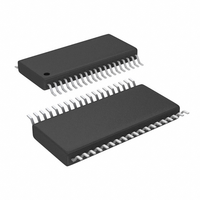
small 38-Pin TSSOP (DBT) Package
APPLICATIONS
•
•
•
DESCRIPTION
The bq20z75 SBS-compliant gas gauge and
protection IC is a single IC solution designed for
battery-pack or in-system installation. The bq20z75
measures and maintains an accurate record of
available charge in Li-ion or Li-polymer batteries
using its integrated high-performance analog
peripherals, monitors capacity change, battery
impedance, open-circuit voltage, and other critical
parameters of the battery pack as well and reports
the information to the system host controller over a
serial-communication bus. Together with the
integrated analog front-end (AFE) short-circuit and
overload protection the bq20z75 maximizes
functionality, safety and minimize external component
count, cost and size in smart battery circuits.
The implemented Impedance Track™ gas gauging
technology continuously analyzes the battery
impedance, resulting in superior gas-gauging
accuracy. This enables remaining capacity to be
calculated with discharge rate, temperature, and cell
aging all accounted for during each stage of every
cycle with high accuracy.
Notebook PCs
Medical and Test Equipment
Portable Instrumentation
Table 1. AVAILABLE OPTIONS
PACKAGE
TA
–40°C to
85°C
(1)
(2)
38-PIN TSSOP (DBT)
Tube (1)
38-PIN TSSOP (DBT)
Tape and Reel (2)
bq20z75DBT
bq20z75DBTR
bq20z75DBT-v160
bq20z75DBTR-v160
A single tube quantity is 50 units.
A single reel quantity is 2000 units
1
2
Please be aware that an important notice concerning availability, standard warranty, and use in critical applications of Texas
Instruments semiconductor products and disclaimers thereto appears at the end of this data sheet.
IMPEDANCE TRACK is a trademark of Texas Instruments.
PRODUCTION DATA information is current as of publication date.
Products conform to specifications per the terms of the Texas
Instruments standard warranty. Production processing does not
necessarily include testing of all parameters.
Copyright © 2007–2008, Texas Instruments Incorporated
�bq20z75
SLUS723C – JULY 2007 – REVISED JULY 2008
www.ti.com
This integrated circuit can be damaged by ESD. Texas Instruments recommends that all integrated circuits be handled with
appropriate precautions. Failure to observe proper handling and installation procedures can cause damage.
ESD damage can range from subtle performance degradation to complete device failure. Precision integrated circuits may be more
susceptible to damage because very small parametric changes could cause the device not to meet its published specifications.
SYSTEM PARTITIONING DIAGRAM
VSS
BAT
VSS
PACK
CHG
DSG
GPOD
PMS
ZVCHG
PFIN
¯¯¯¯
SAFE
Pack +
RBI
Fuse Blow
Detection and
Logic
SMBD
SMBC
Oscillator
N-Channel FET
Drive
Power Mode
Control
AFE HW Control
Watchdog
Pre Charge FET
& PGOD Drive
MSRT
¯¯¯¯¯
RESET
¯¯¯¯¯¯
SMBD
SMBC
SMB 1.1
System Control
ALERT
¯¯¯¯¯¯
VCELL+
Data Flash
Memory
Charging
Algorithm
Voltage
Measurement
Over
Temperature
Protection
Over- & UnderVoltage
Protection
Cell Voltage
Multiplexer
Impedance
Track ™
Gas Gauging
VC1
VC1
VDD
VC2
VC2
OUT
VC3
VC3
CD
VC4
VC4
GND
Cell Balancing
VC5
bq294xx
ASRN
GSRN
ASRP
HW Over
Current &
Short Circuit
Protection
Coloumb
Counter
GSRP
Over Current
Protection
TS2
TS1
Temperature
Measurement
TOUT
SHA-1
Authentication
REG33
REG25
Regulators
bq20z75
Pack RSNS
5mΩ – 20mΩ typical
TSSOP (PW)
(TOP VIEW)
DSG
PACK
VCC
ZVCHG
GPOD
PMS
VSS
REG33
TOUT
VCELL+
ALERT
PRES
TS1
TS2
PFIN
SAFE
SMBD
SMBC
NC
2
1
2
3
4
5
6
7
8
9
10
11
12
13
14
15
16
17
18
19
38
37
36
35
34
33
32
31
30
29
28
27
26
25
24
23
22
21
20
CHG
BAT
VC1
VC2
VC3
VC4
VC5
ASRP
ASRN
RESET
VSS
RBI
REG25
VSS
MRST
GSRN
GSRP
VSS
VSS
Submit Documentation Feedback
Copyright © 2007–2008, Texas Instruments Incorporated
Product Folder Link(s): bq20z75
�bq20z75
www.ti.com
SLUS723C – JULY 2007 – REVISED JULY 2008
TERMINAL FUNCTIONS
TERMINAL
(1)
I/O (1)
DESCRIPTION
NO.
NAME
1
DSG
O
2
PACK
IA, P
3
VCC
P
Positive device supply input. Connect to the center connection of the CHG FET and DSG FET to
ensure device supply either from battery stack or battery pack input
4
ZVCHG
O
P-channel pre-charge FET gate drive
5
GPOD
OD
6
PMS
I
Pre-charge mode setting input. Connect to PACK to enable 0v pre-charge using charge FET
connected at CHG pin. Connect to VSS to disable 0V pre-charge using charge FET connected at
CHG pin.
7
VSS
P
Negative device power supply input. Connect all VSS pins together for operation of device
3.3V regulator output. Connect at least a 2.2mF capacitor to REG33 and VSS
High side N-channel discharge FET gate drive
Battery pack input voltage sense input. It also serves as device wake up when device is in shutdown
mode.
High voltage general purpose open drain output. Can be configured to be used in pre-charge
condition
8
REG33
P
9
TOUT
P
Termistor bias supply output
10
VCELL+
-
Internal cell voltage multiplexer and amplifier output. Connect a 0.1mF capacitor to VCELL+ and VSS
11
ALERT
I/OD
Alert output. In case of short circuit condition, overload condition and watchdog time out this pin will
be triggered.
12
PRES
I/OD
System / Host present input. Pull up to TOUT
13
TS1
IA
Temperature sensor 1 input
14
TS2
IA
15
PFIN
I/OD
Fuse blow detection input
Temperature sensor 2 input
16
SAFE
I/OD
blow fuse signal output
17
SMBD
I/OD
SMBus data line
18
SMBC
I/OD
19
NC
-
Not Connected
20
VSS
P
Negative device power supply input. Connect all VSS pins together for operation of device.
SMBus clock line
21
VSS
P
Negative device power supply input. Connect all VSS pins together for operation of device.
22
GSRP
IA
Coulomb counter differential input. Connect to one side of the sense resistor
23
GSRN
IA
Coulomb counter differential input. Connect to one side of the sense resistor
24
MRST
I
Reset input for internal CPU core. connect to RESET for correct operation of device.
25
VSS
P
Negative device power supply input. Connect all VSS pins together for operation of device.
26
REG25
P
2.5V regulator output. Connect at least a 1mF capacitor to REG25 and VSS
27
RBI
P
RAM backup input. Connect a capacitor to this pin and VSS to protect loss of RAM data in case of
short-circuit condition
28
VSS
P
Negative device power supply input. Connect all VSS pins together for operation of device
29
RESET
O
Reset output. Connect to MSRT.
30
ASRN
IA
Short-circuit and overload detection differential input
31
ASRP
IA
Short-circuit and overload detection differential input
32
VC5
IA,P
Cell voltage sense input and cell balancing input for the negative voltage of the bottom cell in cell
stack.
33
VC4
IA,P
Cell voltage sense input and cell balancing input for the positive voltage of the bottom cell and the
negative voltage of the second lowest cell in cell stack.
34
VC3
IA,P
Cell voltage sense input and cell balancing input for the positive voltage of the second lowest cell in
cell stack and the negative voltage of the second highest cell in 4 cell applications.
35
VC2
IA,P
Cell voltage sense input and cell balancing input for the positive voltage of the second highest cell
and the negative voltage of the highest cell in 4 cell applications. Connect to VC3 in 2 cell stack
applications
36
VC1
IA,P
Cell voltage sense input and cell balancing input for the positive voltage of the highest cell in cell
stack in 4 cell applications. Connect to VC2 in 3 or 2 cell stack applications
I = Input, IA = Analog input, I/O = Input/output, I/OD = Input/Open-drain output, O = Output, OA = Analog output, P = Power
Submit Documentation Feedback
Copyright © 2007–2008, Texas Instruments Incorporated
Product Folder Link(s): bq20z75
3
�bq20z75
SLUS723C – JULY 2007 – REVISED JULY 2008
www.ti.com
TERMINAL FUNCTIONS (continued)
TERMINAL
NO.
NAME
I/O (1)
DESCRIPTION
37
BAT
O
Battery stack voltage sense input
38
CHG
O
High side N-channel charge FET gate drive
Absolute Maximum Ratings
Over Operating Free-Air Temperature (unless otherwise noted)
V MAX
V IN
(1)
DESCRIPTION
PIN
Supply voltage range
VBAT, VCC
Input voltage range
UNIT
–0.3V to 34V
PACK, PMS
–0.3V to 34V
VC(n)-VC(n+1); n = 1,
2, 3, 4
–0.3V to 8.5V
VC1, VC2, VC3, VC4
–0.3V to 34V
VC5
–0.3V to 1.0V
PFIN, SMBD, SMBC,
DISP
–0.3V to 6.0V
TS1, TS2, VCELL+,
PRES; ALERT
–0.3 V to V REG25 + 0.3 V
MRST, GSRN, GSRP,
RBI
–0.3 V to V REG25 + 0.3 V
ASRN, ASRP
–1.0V to 1.0V
DSG, CHG, GPOD
V OUT
Output voltage range
–0.3V to 34V
ZVCHG
–0.3V to V BAT
TOUT, ALERT,
REG33,
–0.3 V to 6.0V
RESET
–0.3 V to 7.0V
REG25, SAFE, TOUT
–0.3V to 2.75V
PRES, PFIN, SMBD,
SMBC
50mA
I SS
Maximum combined sink current for input pins
TA
Operating free-air temperature range
–40°C to 85°C
TF
Functional temperature
–40°C to 100°C
T stg
Storage temperature range
–65°C to 150°C
T sld
Lead temperature (soldering, 10s)
(1)
4
300°C
Stresses beyond those listed under absolute maximum ratings may cause permanent damage to the device. These are stress ratings
only, and functional operation of the device at these or any other conditions beyond those indicated under recommended operating
conditions is not implied. Exposure to absolute-maximum-rated conditions for extended periods may affect device reliability.
Submit Documentation Feedback
Copyright © 2007–2008, Texas Instruments Incorporated
Product Folder Link(s): bq20z75
�bq20z75
www.ti.com
SLUS723C – JULY 2007 – REVISED JULY 2008
Recommended Operating Conditions
over operating free-air temperature range (unless otherwise noted)
PARAMETER
PIN
V SUP
Supply voltage
VCC, VBAT
MIN
4.5
V
Minimum startup voltage
VCC, BAT, PACK
5.5
NOM
MAX
25
UNIT
V
V
STARTUP
VIN
Input Voltage Range
VC(n)–VC(n+1); n = 1,2,3,4
0
5
V
VC1, VC2, VC3, VC4
0
VSUP
V
VC5
0
0.5
V
ASRN, ASRP
–0.5
0.5
V
PACK, PMS
0
25
V
0
25
V
1
mA
VGPOD
Output Voltage Range
GPOD
AGPOD
Drain Current (1)
GPOD
CREG25
2.5V LDO Capacitor
REG25
1
µF
CREG33
3.3V LDO Capacitor
REG33
2.2
µF
CVCELL+
Cell Voltage Output Capacitor
VCELL+
0.1
µF
1
kΩ
CPACK
(1)
(2)
PACK input block resistor
(2)
PACK
Use external resistor to limit current to GPOD to 1mA in high voltage application.
External resistor to limit inrush current PACK pin required.
Electrical Characteristics
over operating free-air temperature range (unless otherwise noted), TA = –40°C to 85°C, VREG25 = 2.41 V to 2.59 V, VBAT =
14V, CREG25 = 1µF, CREG33 = 2.2µF; typical values at TA = 25°C (unless otherwise noted)
PARAMETER
TEST CONDITIONS
MIN
TYP
MAX
UNIT
SUPPLY CURRENT
INORMAL
Firmware running
ISLEEP
Sleep Mode
ISHUTDOW
550
µA
CHG FET on; DSG FET on
124
µA
CHG FET off; DSG FET on
90
µA
CHG FET off; DSG FET off
52
µA
Shutdown Mode
0.1
1
µA
1
µA
1.25
10
mV
VWAKE = 1.0mV;
IWAKE=0, RSNS1=0, RSNS0=1;
–0.7
0.7
VWAKE = 2.25mV;
IWAKE =1, RSNS1=0, RSNS0=1;
IWAKE =0, RSNS1=1, RSNS0=0;
–0.8
0.8
VWAKE = 4.5mV;
IWAKE =1, RSNS1=1, RSNS0=1;
IWAKE =0, RSNS1=1, RSNS0=0;
–1.0
1.0
VWAKE = 9mV;
IWAKE =1, RSNS1=1, RSNS0=1;
–1.4
1.4
N
SHUTDOWN WAKE; TA = 25°C (unless otherwise noted)
IPACK
Shutdown exit at VSTARTUP threshold
SRx WAKE FROM SLEEP; TA = 25°C (unless otherwise noted)
VWAKE
VWAKE_A
CR
VWAKE_T
CO
tWAKE
Positive or negative wake threshold with
1.00 mV, 2.25 mV, 4.5 mV and 9 mV
programmable options
Accuracy of VWAKE
mV
Temperature drift of VWAKE accuracy
0.5
%/°C
Time from application of current and
wake of bq20z75
1
10
1.80
1.90
ms
POWER-ON RESET
VIT–
Negative-going voltage input
Voltage at REG25 pin
1.70
Submit Documentation Feedback
Copyright © 2007–2008, Texas Instruments Incorporated
Product Folder Link(s): bq20z75
V
5
�bq20z75
SLUS723C – JULY 2007 – REVISED JULY 2008
www.ti.com
Electrical Characteristics (continued)
over operating free-air temperature range (unless otherwise noted), TA = –40°C to 85°C, VREG25 = 2.41 V to 2.59 V, VBAT =
14V, CREG25 = 1µF, CREG33 = 2.2µF; typical values at TA = 25°C (unless otherwise noted)
PARAMETER
Vhys
tRST
TEST CONDITIONS
Hysteresis
VIT+ – VIT–
RESET active low time
active low time after power up or
watchdog reset
MIN
TYP
MAX
UNIT
50
150
250
mV
100
250
560
µs
250
500
1000
ms
50
100
150
µs
2.41
2.5
2.59
V
WATCHDOG TIMER
tWDTINT
Watchdog start up detect time
tWDWT
Watchdog detect time
2.5V LDO; IREG33OUT = 0mA; TA = 25°C (unless otherwise noted)
VREG25
Regulator output voltage
4.5 < VCC or BAT < 25V; IREG25OUT
≤16mA; TA = –40°C to 100°C
ΔVREG25
Regulator output change with
temperature
IREG25OUT = 2mA; TA = –40°C to
100°C
Line regulation
5.4 < VCC or BAT < 25V; IREG25OUT
= 2mA
3
10
0.2mA ≤ IREG25OUT ≤ 2mA
7
25
0.2mA ≤ IREG25OUT ≤ 16mA
15
50
5
40
75
mA
3
3.3
3.6
V
TEMP
ΔVREG25L
INE
ΔVREG25L
Load Regulation
OAD
IREG25MA
Current Limit
X
±0.2
drawing current until REG25 = 2V to
0V
%
mV
mV
3.3V LDO; IREG25OUT = 0mA; TA = 25°C (unless otherwise noted)
VREG33
Regulator output voltage
4.5 < VCC or BAT < 25V; IREG33OUT
≤ 25mA; TA = –40°C to 100°C
ΔVREG33
Regulator output change with
temperature
IREG33OUT = 2mA; TA = –40°C to
100°C
Line regulation
5.4 < VCC or BAT < 25V; IREG33OUT
= 2mA
3
17
0.2mA ≤ IREG33OUT ≤ 2mA
7
17
0.2mA ≤ IREG33OUT ≤ 25mA
40
100
100
145
TEMP
ΔVREG33L
INE
ΔVREG33L
Load Regulation
OAD
IREG33MA
Current Limit
X
±0.2
drawing current until REG33 = 3V
25
short REG33 to VSS, REG33 = 0V
12
%
65
mV
mV
mA
THERMISTOR DRIVE
VTOUT
RDS(ON)
Output voltage
ITOUT = 0mA; TA = 25°C
TOUT pass element resistance
ITOUT = 1mA; RDS(ON) = (VREG25 –
VTOUT) / 1mA; TA = –40°C to 100°C
VREG25
V
50
100
Ω
VCELL+ HIGH VOLTAGE TRANSLATION
VC(n) – VC(n+1) = 0V; TA = –40°C
to 100°C
0.950
0.975
1
VC(n) – VC(n+1) = 4.5V; TA = –40°C
to 100°C
0.275
0.3
0.375
internal AFE reference voltage ; TA =
–40°C to 100°C
0.965
0.975
0.985
EF
VVCELL+P
ACK
Voltage at PACK pin; TA = –40°C to
100°C
0.98*VPAC
K/18
VPACK/18
1.02*VPA
CK/18
VVCELL+B
Voltage at BAT pin; TA = –40°C to
100°C
0.98*VBAT/
18
VBAT/18
1.02*VBA
T/18
VVCELL+O
UT
VVCELL+R
Translation output
AT
CMMR
K
6
Common mode rejection ratio
Cell scale factor
VCELL+
40
dB
K= {VCELL+ output (VC5=0V;
VC4=4.5V) – VCELL+ output
(VC5=0V; VC4=0V)}/4.5
0.147
0.150
0.153
K= {VCELL+ output (VC2=13.5V;
VC1=18V) – VCELL+ output
(VC5=13.5V; VC1=13.5V)}/4.5
0.147
0.150
0.153
Submit Documentation Feedback
V
Copyright © 2007–2008, Texas Instruments Incorporated
Product Folder Link(s): bq20z75
�bq20z75
www.ti.com
SLUS723C – JULY 2007 – REVISED JULY 2008
Electrical Characteristics (continued)
over operating free-air temperature range (unless otherwise noted), TA = –40°C to 85°C, VREG25 = 2.41 V to 2.59 V, VBAT =
14V, CREG25 = 1µF, CREG33 = 2.2µF; typical values at TA = 25°C (unless otherwise noted)
PARAMETER
MIN
TYP
VC(n) – VC(n+1) = 0V; VCELL+ =
0V; TA = –40°C to 100°C
12
18
VVCELL+O CELL offset error
CELL output (VC2 = VC1 = 18V) –
CELL output (VC2 = VC1 = 0V)
–18
–1
18
mV
IVCnL
VC1, VC2, VC3, VC4, VC5 = 3V
–1
0.01
1
mA
200
400
600
Ω
IVCELL+OU
T
Drive Current to VCELL+ capacitor
VC(n) pin leakage current
TEST CONDITIONS
MAX
UNIT
mA
CELL BALANCING
RBAL
internal cell balancing FET resistance
RDS(on) for internal FET switch at VDS
= 2V; TA = 25°C
HARDWARE SHORT CIRCUIT AND OVERLOAD PROTECTION; TA = 25°C (unless otherwise noted)
V(OL)
V(SCC)
V(SCD)
OL detection threshold voltage accuracy
SCC detection threshold voltage
accuracy
SCD detection threshold voltage
accuracy
tda
Delay time accuracy
tpd
Protection circuit propagation delay
VOL = 25mV (min)
15
25
35
VOL = 100mV; RSNS = 0, 1
90
100
110
VOL = 205mV (max)
185
205
225
VSCC = 50mV (min)
30
50
70
VSCC = 200mV; RSNS = 0, 1
180
200
220
VSCC = 475mV (max)
428
475
523
VSCD = –50mV (min)
–30
–50
–70
VSCD = –200mV; RSNS = 0, 1
–180
–200
–220
VSCD = –475mV (max)
–428
–475
–523
mV
mV
mV
±15.25
ms
50
ms
FET DRIVE CIRCUIT; TA = 25°C (unless otherwise noted)
VDSGON
DSG pin output on voltage
VDSGON = VDSG – VPACK; VGS =
10MΩ;DSG and CHG on; TA =
–40°C to 100°C
8
12
16
V
VCHGON
CHG pin output on voltage
VCHGON = VCHG – VBAT; VGS =
10MΩ;DSG and CHG on; TA =
–40°C to 100°C
8
12
16
V
VDSGOFF
DSG pin output off voltage
VDSGOFF = VDSG – VPACK
0.2
V
VCHGOFF
CHG pin output off voltage
VCHGOFF = VCHG – VBAT
0.2
V
Rise time
CL=4700pF; VPACK ≤ DSG ≤VPACK +
4V
400
1000
CL=4700pF; VBAT ≤ CHG ≤VBAT + 4V
400
1000
CL=4700pF; VPACK + VDSGON ≤ DSG
≤VPACK + 1V
40
200
CL=4700pF; VBAT + VCHGON ≤ CHG
≤VBAT + 1V
40
200
3.5
3.7
tR
tF
VZVCHG
Fall time
ZVCHG clamp voltage
ms
ms
BAT = 4.5V
3.3
V
LOGIC; TA = –40°C to 100°C (unless otherwise noted)
RPULLUP
VOL
Internal pullup resistance
Logic low output voltage level
ALERT
60
100
200
RESET
1
3
6
ALERT
0.2
RESET; VBAT = 7V; VREG25 = 1.5V; I
RESET = 200mA
0.4
GPOD; IGPOD = 50mA
0.6
kΩ
V
LOGIC SMBC, SMBD, PFIN, PRES, SAFE, ALERT
VIH
High-level input voltage
VIL
Low-level input voltage
2.0
V
0.8
Submit Documentation Feedback
Copyright © 2007–2008, Texas Instruments Incorporated
Product Folder Link(s): bq20z75
V
7
�bq20z75
SLUS723C – JULY 2007 – REVISED JULY 2008
www.ti.com
Electrical Characteristics (continued)
over operating free-air temperature range (unless otherwise noted), TA = –40°C to 85°C, VREG25 = 2.41 V to 2.59 V, VBAT =
14V, CREG25 = 1µF, CREG33 = 2.2µF; typical values at TA = 25°C (unless otherwise noted)
PARAMETER
TEST CONDITIONS
MIN
SAFE, IL = –0.5 mA
VOL
Low-level output voltage
PRES, PFIN, ALERT, IL = 7 mA;
CI
Input capacitance
I(SAFE)
SAFE source currents
SAFE active, SAFE = VREG25 –0.6 V
Ilkg(SAFE)
SAFE leakage current
SAFE inactive
Ilkg
Input leakage current
ADC
MAX
UNIT
VREG25–0.
5
Output voltage high (1)
VOH
TYP
V
0.4
V
5
pF
–3
mA
–0.2
0.2
µA
1
µA
VREG25+
0.2
V
(2)
Input voltage range
TS1,TS2, using external Vref
–0.2
Conversion time
31.5
Resolution (no missing codes)
16
Effective resolution
14
bits
15
bits
±0.03 %FSR (3)
Integral nonlinearity
Offset error (4)
Offset error drift (4)
ms
TA = 25°C to 85°C
Full-scale error (5)
Full-scale error drift
140
250
µV
2.5
18
mV/°C
±0.1%
±0.7%
50
Effective input resistance (6)
PPM/°C
8
MΩ
COULOMB COUNTER
Input voltage range
–0.20
Conversion time
Single conversion
Effective resolution
Single conversion
Integral nonlinearity
Offset error
(7)
250
bits
–0.1 V to 0.20 V
±0.007
–0.20 V to –0.1 V
±0.007
TA = 25°C to 85°C
%FSR
µV
2.45
µV/°C
±0.35%
Full-scale error drift
Effective input resistance (10)
±0.034
10
0.4
(9)
V
ms
15
Offset error drift
Full-scale error (8)
0.20
150
TA = 25°C to 85°C
PPM/°C
2.5
MΩ
INTERNAL TEMPERATURE SENSOR
V(TEMP)
Temperature sensor voltage (11)
–2.0
mV/°C
VOLTAGE REFERENCE
Output voltage
1.215
Output voltage drift
1.225
65
1.230
V
PPM/°C
HIGH FREQUENCY OSCILLATOR
f(OSC)
Operating frequency
4.194
MHz
(1)
(2)
(3)
(4)
(5)
(6)
RC[0:7] bus
Unless otherwise specified, the specification limits are valid at all measurement speed modes
Full-scale reference
Post-calibration performance and no I/O changes during conversion with SRN as the ground reference
Uncalibrated performance. This gain error can be eliminated with external calibration.
The A/D input is a switched-capacitor input. Since the input is switched, the effective input resistance is a measure of the average
resistance.
(7) Post-calibration performance
(8) Reference voltage for the coulomb counter is typically Vref/3.969 at VREG25 = 2.5 V, TA = 25°C.
(9) Uncalibrated performance. This gain error can be eliminated with external calibration.
(10) The CC input is a switched capacitor input. Since the input is switched, the effective input resistance is a measure of the average
resistance.
(11) –53.7 LSB/°C
8
Submit Documentation Feedback
Copyright © 2007–2008, Texas Instruments Incorporated
Product Folder Link(s): bq20z75
�bq20z75
www.ti.com
SLUS723C – JULY 2007 – REVISED JULY 2008
Electrical Characteristics (continued)
over operating free-air temperature range (unless otherwise noted), TA = –40°C to 85°C, VREG25 = 2.41 V to 2.59 V, VBAT =
14V, CREG25 = 1µF, CREG33 = 2.2µF; typical values at TA = 25°C (unless otherwise noted)
PARAMETER
f(EIO)
Frequency error
t(SXO)
Start-up time (14)
TEST CONDITIONS
(12) (13)
TA = 20°C to 70°C
MIN
TYP
MAX
–3%
0.25%
3%
–2%
0.25%
2%
2.5
5
UNIT
ms
LOW FREQUENCY OSCILLATOR
f(LOSC)
f(LEIO)
t(LSXO)
(12)
(13)
(14)
(15)
Operating frequency
Frequency error (13)
Start-up time
32.768
(15)
TA = 20°C to 70°C
kHz
–2.5%
0.25%
2.5%
–1.5%
0.25%
1.5%
(14)
500
µs
The frequency error is measured from 4.194 MHz.
The frequency drift is included and measured from the trimmed frequency at VREG25 = 2.5V, TA = 25°C
The startup time is defined as the time it takes for the oscillator output frequency to be ±3%
The frequency error is measured from 32.768 kHz.
Data Flash Characteristics Over Recommended Operating Temperature and Supply Voltage
Typical Values at TA = 25°C and VREG25= 2.5 V (unless otherwise noted)
PARAMETER
TEST CONDITIONS
MIN
Data retention
Flash programming write-cycles
t(ROWPROG)
Row programming time
See
TYP
MAX
UNIT
10
Years
20k
Cycles
(1)
t(MASSERASE) Mass-erase time
t(PAGEERASE) Page-erase time
2
ms
200
ms
20
ms
I(DDPROG)
Flash-write supply current
5
10
mA
I(DDERASE)
Flash-erase supply current
5
10
mA
V(RBI) > V(RBI)MIN , VREG25 < VIT–,
TA = 85°C
1000
2500
V(RBI) > V(RBI)MIN , VREG25 < VIT–,
TA = 25°C
90
220
RAM BACKUP
I(RB)
RB data-retention input current
V(RB)
RB data-retention input voltage (1)
(1)
1.7
nA
V
Assured by design. Not production tested.
SMBus Timing Characteristics
TA = –40°C to 85°C Typical Values at TA = 25°C and V(REG25) = 2.5 V (Unless Otherwise Noted)
PARAMETER
TEST CONDITIONS
MIN
TYP
UNIT
100
kHz
SMBus operating frequency
Slave mode, SMBC 50% duty cycle
fMAS
SMBus master clock frequency
Master mode, No clock low slave
extend
t(BUF)
Bus free time between start and stop
(see Figure 1)
4.7
µs
t(HD:STA)
Hold time after (repeated) start (see Figure 1)
4.0
µs
t(SU:STA)
Repeated start setup time (see Figure 1)
4.7
µs
t(SU:STO)
Stop setup time (see Figure 1)
4.0
µs
Receive mode
0
ns
Transmit mode
300
t(HD:DAT)
t(SU:DAT)
Data hold time (see Figure 1)
Data setup time (see Figure 1)
10
MAX
fSMB
51.2
250
Submit Documentation Feedback
Copyright © 2007–2008, Texas Instruments Incorporated
Product Folder Link(s): bq20z75
kHz
ns
9
�bq20z75
SLUS723C – JULY 2007 – REVISED JULY 2008
www.ti.com
SMBus Timing Characteristics (continued)
TA = –40°C to 85°C Typical Values at TA = 25°C and V(REG25) = 2.5 V (Unless Otherwise Noted)
PARAMETER
TEST CONDITIONS
Error signal/detect (see Figure 1)
t(LOW)
Clock low period (see Figure 1)
t(HIGH)
Clock high period (see Figure 1)
See
(2)
t(LOW:SEXT)
Cumulative clock low slave extend time
See
t(LOW:MEXT) Cumulative clock low master extend time (see
Figure 1)
tf
tr
(1)
(2)
(3)
(4)
(5)
(6)
See
MIN
(1)
t(TIMEOUT)
TYP
25
MAX
UNIT
35
µs
50
µs
(3)
25
µs
See
(4)
10
µs
Clock/data fall time
See
(5)
300
ns
Clock/data rise time
See
(6)
1000
ns
4.7
µs
4.0
The bq20z75 times out when any clock low exceeds t(TIMEOUT).
t(HIGH), Max, is the minimum bus idle time. SMBC = SMBD = 1 for t > 50 ms causes reset of any transaction involving bq20z75 that is in
progress. This specification is valid when the NC_SMB control bit remains in the default cleared state (CLK[0]=0).
t(LOW:SEXT) is the cumulative time a slave device is allowed to extend the clock cycles in one message from initial start to the stop.
t(LOW:MEXT) is the cumulative time a master device is allowed to extend the clock cycles in one message from initial start to the stop.
Rise time tr = VILMAX – 0.15) to (VIHMIN + 0.15)
Fall time tf = 0.9VDD to (VILMAX – 0.15)
t(LOW)
tr
t(HD:STA)
tf
SCLK
t(HD:STA)
t(HIGH)
t(HD:DAT)
t(SU:STA)
t(SU:STO)
t(SU:DAT)
SDATA
t(BUF)
P
S
S
P
Start
Stop
t(LOW:SEXT)
SCLKACK
t(LOW:MEXT)
(1)
SCLKACK
t(LOW:MEXT)
(1)
t(LOW:MEXT)
SCLK
SDATA
(1)
SCLKACK is the acknowledge-related clock pulse generated by the master.
Figure 1. SMBus Timing Diagram
10
Submit Documentation Feedback
Copyright © 2007–2008, Texas Instruments Incorporated
Product Folder Link(s): bq20z75
�bq20z75
www.ti.com
SLUS723C – JULY 2007 – REVISED JULY 2008
FEATURE SET
Primary (1st Level) Safety Features
The bq20z75 supports a wide range of battery and system protection features that can easily be configured. The
primary safety features include:
•
•
•
•
•
Cell over/under voltage protection
Charge and Discharge over current
Short Circuit
Charge and Discharge Over temperature
AFE Watchdog
Secondary (2nd Level) Safety Features
The secondary safety features of the bq20z75 can be used to indicate more serious faults via the SAFE (pin 7).
This pin can be used to blow an in-line fuse to permanently disable the battery pack from charging or
discharging. The secondary safety protection features include:
•
•
•
•
•
•
Safety overvoltage
Safety overcurrent in Charge and Discharge
Safety overtemperature in Charge and Discharge
Charge FET and 0 Volt Charge FET fault
Discharge FET fault
AFE communication fault
Charge Control Features
The bq20z75 charge control features include:
•
•
•
•
•
•
Reports the appropriate charging current needed for constant current charging and the appropriate charging
voltage needed for constant voltage charging to a smart charger using SMBus broadcasts.
Determines the chemical state of charge of each battery cell using Impedance Track™ and can reduce the
charge difference of the battery cells in fully charged state of the battery pack gradually using cell balancing
algorithm during charging. This prevents fully charged cells from overcharging and causing excessive
degradation and also increases the usable pack energy by preventing premature charge termination
Supports pre-charging/zero-volt charging
Support fast charging
Supports charge inhibit and charge suspend if battery pack temperature is out of temperature range
Reports charging fault and also indicate charge status via charge and discharge alarms.
Gas Gauging
The bq20z75 uses the Impedance Track™ Technology to measure and calculate the available charge in battery
cells. The achievable accuracy is better than 1% error over the lifetime of the battery and there is no full charge
discharge learning cycle required.
See Theory and Implementation of Impedance Track Battery Fuel-Gauging Algorithm application note (SLUA364)
for further details.
Authentication
The bq20z75 supports authentication by the host using SHA-1.
Power Modes
The bq20z75 supports 3 different power modes to reduce power consumption:
•
In Normal Mode, the bq20z75 performs measurements, calculations, protection decisions and data updates in
1 second intervals. Between these intervals, the bq20z75 is in a reduced power stage.
Submit Documentation Feedback
Copyright © 2007–2008, Texas Instruments Incorporated
Product Folder Link(s): bq20z75
11
�bq20z75
SLUS723C – JULY 2007 – REVISED JULY 2008
•
•
www.ti.com
In Sleep Mode, the bq20z75 performs measurements, calculations, protection decisions and data update in
adjustable time intervals. Between these intervals, the bq20z75 is in a reduced power stage. The bq20z75
has a wake function that enables exit from Sleep mode, when current flow or failure is detected.
In Shutdown Mode the bq20z75 is completely disabled.
CONFIGURATION
Oscillator Function
The bq20z75 fully integrates the system oscillators. Therefore the bq20z75 requires no external components for
this feature.
System Present Operation
The bq20z75 checks the PRES pin periodically (1 s). Connect the PRES pin to TOUT with a 100kΩ resistor. If
PRES input is pulled to ground by external system host, the bq20z75 detects this as system present.
BATTERY PARAMETER MEASUREMENTS
The bq20z75 uses an integrating delta-sigma analog-to-digital converter (ADC) for current measurement, and a
second delta-sigma ADC for individual cell and battery voltage, and temperature measurement.
Charge and Discharge Counting
The integrating delta-sigma ADC measures the charge/discharge flow of the battery by measuring the voltage
drop across a small-value sense resistor between the SRP and SRN pins. The integrating ADC measures bipolar
signals from –0.25 V to 0.25 V. The bq20z75 detects charge activity when VSR = V(SRP)–V(SRN)is positive and
discharge activity when VSR = V(SRP)–V(SRN) is negative. The bq20z75 continuously integrates the signal over
time, using an internal counter. The fundamental rate of the counter is 0.65 nVh.
Voltage
The bq20z75 updates the individual series cell voltages at one second intervals. The internal ADC of the
bq20z75 measures the voltage, scales and calibrates it appropriately. This data is also used to calculate the
impedance of the cell for the Impedance Track™ gas-gauging.
Current
The bq20z75 uses the GSRP and GSRN inputs to measure and calculate the battery charge and discharge
current using a 5 mΩ to 20 mΩ typ. sense resistor.
Auto Calibration
The bq20z75 provides an auto-calibration feature to cancel the voltage offset error across GSRN and GSRP for
maximum charge measurement accuracy. The bq20z75 performs auto-calibration when the SMBus lines stay
low continuously for a minimum of 5 s.
Temperature
The bq20z75 has an internal temperature sensor and 2 external temperature sensor inputs TS1 and TS2 used in
conjunction with two identical NTC thermistors (default are Semitec 103AT) to sense the battery environmental
temperature. The bq20z75 can be configured to use internal or external temperature sensors.
COMMUNICATIONS
The bq20z75 uses SMBus v1.1 with Master Mode and package error checking (PEC) options per the SBS
specification.
SMBus On and Off State
The bq20z75 detects an SMBus off state when SMBC and SMBD are logic-low for ≥ 2 seconds. Clearing this
state requires either SMBC or SMBD to transition high. Within 1 ms, the communication bus is available.
12
Submit Documentation Feedback
Copyright © 2007–2008, Texas Instruments Incorporated
Product Folder Link(s): bq20z75
�bq20z75
www.ti.com
SLUS723C – JULY 2007 – REVISED JULY 2008
SBS and Dataflash Values
Table 2. SBS COMMANDS
SBS
Cmd
Mode
Name
Format
Size in
Bytes
Min
Value
Max
Value
Default
Value
Unit
0x00
R/W
ManufacturerAccess
hex
2
0x0000
0xffff
—
0x01
R/W
RemainingCapacityAlarm
unsigned int
2
0
65535
—
mAh or
10mWh
0x02
R/W
RemainingTimeAlarm
unsigned int
2
0
65535
—
min
0x03
R/W
BatteryMode
hex
2
0x0000
0xffff
—
0x04
R/W
AtRate
signed int
2
–32768
32767
—
mA or 10mW
0x05
R
AtRateTimeToFull
unsigned int
2
0
65535
—
min
0x06
R
AtRateTimeToEmpty
unsigned int
2
0
65535
—
min
0x07
R
AtRateOK
unsigned int
2
0
65535
—
0x08
R
Temperature
unsigned int
2
0
65535
—
0.1°K
0x09
R
Voltage
unsigned int
2
0
20000
—
mV
0x0a
R
Current
signed int
2
–32768
32767
—
mA
0x0b
R
AverageCurrent
signed int
2
–32768
32767
—
mA
0x0c
R
MaxError
unsigned int
1
0
100
—
%
0x0d
R
RelativeStateOfCharge
unsigned int
1
0
100
—
%
0x0e
R
AbsoluteStateOfCharge
unsigned int
1
0
100
—
%
0x0f
R/W
RemainingCapacity
unsigned int
2
0
65535
—
mAh or
10mWh
0x10
R
FullChargeCapacity
unsigned int
2
0
65535
—
mAh or
10mWh
0x11
R
RunTimeToEmpty
unsigned int
2
0
65535
—
min
0x12
R
AverageTimeToEmpty
unsigned int
2
0
65535
—
min
0x13
R
AverageTimeToFull
unsigned int
2
0
65535
—
min
0x14
R
ChargingCurrent
unsigned int
2
0
65535
—
mA
0x15
R
ChargingVoltage
unsigned int
2
0
65535
—
mV
0x16
R
BatteryStatus
unsigned int
2
0x0000
0xffff
—
0x17
R/W
CycleCount
unsigned int
2
0
65535
—
0x18
R/W
DesignCapacity
unsigned int
2
0
65535
—
mAh or
10mWh
0x19
R/W
DesignVoltage
unsigned int
2
7000
16000
14400
mV
0x1a
R/W
SpecificationInfo
unsigned int
2
0x0000
0xffff
0x0031
0x1b
R/W
ManufactureDate
unsigned int
2
0
65535
0
0x1c
R/W
SerialNumber
hex
2
0x0000
0xffff
-
0x20
R/W
ManufacturerName
String
11+1
—
—
Texas
Instruments
ASCII
0x21
R/W
DeviceName
String
7+1
—
—
bq20z75
ASCII
0x22
R/W
DeviceChemistry
String
4+1
—
—
LION
ASCII
0x23
R
ManufacturerData
String
14+1
—
—
—
ASCII
0x2f
R/W
Authenticate
String
20+1
—
—
—
ASCII
0x3c
R
CellVoltage4
unsigned int
2
0
65535
—
mV
0x3d
R
CellVoltage3
unsigned int
2
0
65535
—
mV
0x3e
R
CellVoltage2
unsigned int
2
0
65535
—
mV
0x3f
R
CellVoltage1
unsigned int
2
0
65535
—
mV
Submit Documentation Feedback
Copyright © 2007–2008, Texas Instruments Incorporated
Product Folder Link(s): bq20z75
13
�bq20z75
SLUS723C – JULY 2007 – REVISED JULY 2008
www.ti.com
Table 3. EXTENDED SBS COMMANDS
SBS
Cmd
Mode
Name
Format
Size in
Bytes
Min Value
Max Value
Default
Value
Unit
0x45
R
AFEData
String
11+1
—
—
—
ASCII
0x46
R/W
FETControl
hex
1
0x00
0xff
—
0x4f
R
StateOfHealth
unsigned int
1
0
100
—
0x51
R
SafetyStatus
hex
2
0x0000
0xffff
—
0x53
R
PFStatus
hex
2
0x0000
0xffff
—
0x54
R
OperationStatus
hex
2
0x0000
0xffff
—
0x55
R
ChargingStatus
hex
2
0x0000
0xffff
—
0x57
R
ResetData
hex
2
0x0000
0xffff
—
0x5a
R
PackVoltage
unsigned int
2
0
65535
—
mV
0x5d
R
AverageVoltage
unsigned int
2
0
65535
—
mV
0x60
R/W
UnSealKey
hex
4
0x00000000
0xffffffff
—
0x61
R/W
FullAccessKey
hex
4
0x00000000
0xffffffff
—
0x62
R/W
PFKey
hex
4
0x00000000
0xffffffff
—
0x63
R/W
AuthenKey3
hex
4
0x00000000
0xffffffff
—
0x64
R/W
AuthenKey2
hex
4
0x00000000
0xffffffff
—
0x65
R/W
AuthenKey1
hex
4
0x00000000
0xffffffff
—
0x66
R/W
AuthenKey0
hex
4
0x00000000
0xffffffff
—
0x70
R/W
ManufacturerInfo
String
31+1
—
—
—
0x71
R/W
SenseResistor
unsigned int
2
0
65535
—
0x77
R/W
DataFlashSubClassID
hex
2
0x0000
0xffff
—
0x78
R/W
DataFlashSubClassPage1
hex
32
—
—
—
0x79
R/W
DataFlashSubClassPage2
hex
32
—
—
—
0x7a
R/W
DataFlashSubClassPage3
hex
32
—
—
—
0x7b
R/W
DataFlashSubClassPage4
hex
32
—
—
—
0x7c
R/W
DataFlashSubClassPage5
hex
32
—
—
—
0x7d
R/W
DataFlashSubClassPage6
hex
32
—
—
—
0x7e
R/W
DataFlashSubClassPage7
hex
32
—
—
—
0x7f
R/W
DataFlashSubClassPage8
hex
32
—
—
—
14
Submit Documentation Feedback
%
mΩ
Copyright © 2007–2008, Texas Instruments Incorporated
Product Folder Link(s): bq20z75
�bq20z75
www.ti.com
SLUS723C – JULY 2007 – REVISED JULY 2008
Application Schematics
Submit Documentation Feedback
Copyright © 2007–2008, Texas Instruments Incorporated
Product Folder Link(s): bq20z75
15
�bq20z75
www.ti.com
321
8 7 65
Q4
TPC8017-H
SLUS723C – JULY 2007 – REVISED JULY 2008
8 7 65
8 7 65
Submit Documentation Feedback
2
3
1
Q2
TPC8017-H
321
3 21
16
Copyright © 2007–2008, Texas Instruments Incorporated
Product Folder Link(s): bq20z75
�PACKAGE OPTION ADDENDUM
www.ti.com
14-Oct-2022
PACKAGING INFORMATION
Orderable Device
Status
(1)
Package Type Package Pins Package
Drawing
Qty
Eco Plan
(2)
Lead finish/
Ball material
MSL Peak Temp
Op Temp (°C)
Device Marking
(3)
Samples
(4/5)
(6)
BQ20Z75DBT-V160
ACTIVE
TSSOP
DBT
38
50
RoHS & Green
NIPDAU
Level-2-260C-1 YEAR
-40 to 85
20Z75
Samples
BQ20Z75DBTR-V160
ACTIVE
TSSOP
DBT
38
2000
RoHS & Green
NIPDAU
Level-2-260C-1 YEAR
-40 to 85
20Z75
Samples
(1)
The marketing status values are defined as follows:
ACTIVE: Product device recommended for new designs.
LIFEBUY: TI has announced that the device will be discontinued, and a lifetime-buy period is in effect.
NRND: Not recommended for new designs. Device is in production to support existing customers, but TI does not recommend using this part in a new design.
PREVIEW: Device has been announced but is not in production. Samples may or may not be available.
OBSOLETE: TI has discontinued the production of the device.
(2)
RoHS: TI defines "RoHS" to mean semiconductor products that are compliant with the current EU RoHS requirements for all 10 RoHS substances, including the requirement that RoHS substance
do not exceed 0.1% by weight in homogeneous materials. Where designed to be soldered at high temperatures, "RoHS" products are suitable for use in specified lead-free processes. TI may
reference these types of products as "Pb-Free".
RoHS Exempt: TI defines "RoHS Exempt" to mean products that contain lead but are compliant with EU RoHS pursuant to a specific EU RoHS exemption.
Green: TI defines "Green" to mean the content of Chlorine (Cl) and Bromine (Br) based flame retardants meet JS709B low halogen requirements of