bq20z80-V101
www.ti.com
SLUS625D – SEPTEMBER 2004 – REVISED OCTOBER 2005
SBS 1.1-COMPLIANT GAS GAUGE ENABLED WITH IMPEDANCE TRACK™
TECHNOLOGY FOR USE WITH THE bq29312A
FEATURES
•
•
•
•
•
•
•
•
•
•
•
•
•
•
•
Patented Impedance Track™ Technology
Accurately Measures Available Charge in
Li-Ion and Li-Polymer Batteries
Better than 1% Error Over Lifetime of the
Battery
Instant Accuracy – No Learning Cycle
Required
Supports the Smart Battery Specification SBS
V1.1
Works With the TI bq29312A Analog
Front-End (AFE) Protection IC to Provide
Complete Pack Electronics Solution
Full Array of Programmable Voltage, Current,
and Temperature Protection Features
Integrated Time Base Removes Need for
External Crystal with Optional Crystal Input
Electronics for 7.2-V, 10.8-V or 14.4-V Battery
Packs With Few External Components
Based on a Powerful Low-Power RISC CPU
Core With High-Performance Peripherals
Integrated Field Programmable FLASH
Memory Eliminates the Need for External
Configuration Memory
Measures Charge Flow Using a
High-Resolution, 16-Bit Integrating
Delta-Sigma Converter
– Better Than 0.65-nVh of Resolution
– Self-Calibrating
– Offset Error Less Than 1-µV
Uses 16-Bit Delta-Sigma Converter for
Accurate Voltage and Temperature
Measurements
Extensive Data Reporting Options For
Improved System Interaction
Optional Pulse Charging Feature for Improved
Charge Times
Drives 3-, 4- or 5-Segment LED Display for
Remaining Capacity Indication
•
38-Pin TSSOP (DBT)
APPLICATIONS
•
•
•
Notebook PCs
Medical and Test Equipment
Portable Instrumentation
DESCRIPTION
The bq20z80 SBS-compliant gas gauge IC,
incorporating patented Impedance Track technology,
is designed for battery-pack or in-system installation.
The bq20z80 measures and maintains an accurate
record of available charge in Li-ion or Li-polymer
batteries using its integrated high-performance
analog peripherals. The bq20z80 monitors capacity
change, battery impedance, open-circuit voltage, and
other critical parameters of the battery pack, and
reports the information to the system host controller
over a serial-communication bus. It is designed to
work with the bq29312A analog front-end (AFE)
protection IC to maximize functionality and safety,
and minimize component count and cost in smart
battery circuits.
The Impedance Track technology continuously
analyzes the battery impedance, resulting in superior
gas-gauging accuracy. This enables remaining
capacity to be calculated with discharge rate,
temperature, and cell aging all accounted for during
each stage of every cycle.
AVAILABLE OPTIONS
PACKAGE
TA
38-PIN TSSOP (DBT)
Tube
38-PIN TSSOP (DBT)
Tape & Reel
–40°C to
85°C
bq20z80DBT-V101 (1)
bq20z80DBTR-V101 (2)
(1)
(2)
A single tube quantity is 50 units.
A single reel quantity is 2000 units
Please be aware that an important notice concerning availability, standard warranty, and use in critical applications of Texas
Instruments semiconductor products and disclaimers thereto appears at the end of this data sheet.
IMPEDANCE TRACK is a trademark of Texas Instruments.
PRODUCTION DATA information is current as of publication date.
Products conform to specifications per the terms of the Texas
Instruments standard warranty. Production processing does not
necessarily include testing of all parameters.
Copyright © 2004–2005, Texas Instruments Incorporated
�bq20z80-V101
www.ti.com
SLUS625D – SEPTEMBER 2004 – REVISED OCTOBER 2005
These devices have limited built-in ESD protection. The leads should be shorted together or the device
placed in conductive foam during storage or handling to prevent electrostatic damage to the MOS gates.
TSSOP (DBT)
(TOP VIEW)
VIN
TS1
TS2
PU
PRES
SCLK
SAFE
VDDD
RBI
SDATA
VSSD
SAFE
NC
NC
SMBC
SMBD
DISP
PFIN
VSSD
1
2
3
4
5
6
7
8
9
10
11
12
13
14
15
16
17
18
19
38
37
36
35
34
33
32
31
30
29
28
VSSD
NC
NC
CLKOUT
XCK1 / VSSA
XCK2 / ROSC
FILT
VDDA
VSSA
VSSA
27
SR1
SR2
26
25
24
23
22
21
20
MRST
XALERT
LED1
LED2
LED3
LED4
LED5
NC - No internal connection
TERMINAL FUNCTIONS
TERMINAL
NO.
(1)
2
NAME
I/O (1)
DESCRIPTION
1
VIN
I
Voltage measurement input from the AFE
2
TS1
I
1st Thermistor voltage input connection to monitor temperature
3
TS2
I
2nd Thermistor voltage input connection to monitor temperature
4
PU
O
Output to pull up the PRES pin for system detection
5
PRES
I
Active low input to sense system insertion and typically requires additional ESD protection
6
SCLK
I/OD
7
SAFE
O
Active high output to enforce additional level of safety protection; e.g., fuse blow. (Inverse of pin 12)
8
VDDD
P
Positive supply for digital circuitry and I/O pins
9
RBI
P
Backup power to the bq20z80 data registers during periods of low operating voltage. RBI accepts a
storage capacitor or a battery input.
10
SDATA
I/O
Data transfer to and from the AFE
12
SAFE
O
Active low output to enforce additional level of safety protection; e.g., fuse blow. (Inverse of pin 7)
13
NC
–
Not used— leave floating
14
NC
–
Not used— leave floating
15
SMBC
I/OD
SMBus clock open-drain bidirectional pin used to clock the data transfer to and from the bq20z80
16
SMBD
I/OD
SMBus data open-drain bidirectional pin used to transfer address and data to and from the bq20z80
17
DISP
I
Display control for the LEDs. This pin is typically connected to bq29312A REG via a 100-kΩ resistor
and a push-button switch to VSSD.
18
PFIN
I
Active low input to detect secondary protector output status and allows the bq20z80 to report the
status of the 2nd level protection output
20
LED5
O
LED5 display segment that drives an external LED depending on the firmware configuration
21
LED4
O
LED4 display segment that drives an external LED depending on the firmware configuration
Communication clock to the AFE
I = Input, IA = Analog input, I/O = Input/output, I/OD = Input/Open-drain output, O = Output, OA = Analog output, P = Power
�bq20z80-V101
www.ti.com
SLUS625D – SEPTEMBER 2004 – REVISED OCTOBER 2005
TERMINAL FUNCTIONS (continued)
TERMINAL
I/O (1)
DESCRIPTION
NO.
NAME
22
LED3
O
LED3 display segment that drives an external LED depending on the firmware configuration
23
LED2
O
LED2 display segment that drives an external LED depending on the firmware configuration
24
LED1
O
LED1 display segment that drives an external LED depending on the firmware configuration
25
XALERT
I
Input from bq29312A XALERT output.
26
MRST
I
Master reset input that forces the device into reset when held high
27
SR2
IA
Connections for a small-value sense resistor to monitor the battery charge- and discharge-current flow
28
SR1
IA
Connections for a small-value sense resistor to monitor the battery charge- and discharge-current flow
31
VDDA
P
Positive supply for analog circuitry
32
FILT
IA
Analog input connected to the external PLL filter components which are a 150-pF capacitor to VSSA, in
parallel with a 61.9-kΩ resistor and a 2200-pF capacitor in series. Place these components as close as
possible to the bq20z80 to ensure optimal performance.
33
XCK2/ROSC
O
32.768-kHz crystal oscillator output pin or connected to a 100k, 50ppm or better resistor if the internal
oscillator is used
34
XCK1/VSSA
I
32.768-kHz crystal oscillator input pin or connected to VSSA if the internal oscillator is used
35
CLKOUT
O
32.768-kHz output for the bq29312. This pin should be directly connected to the AFE.
36
NC
-
Not used— leave floating
37
NC
-
Not used— leave floating
11, 19,
38
VSSD
P
Negative supply for digital circuitry
29, 30
VSSA
P
Negative supply for analog circuitry.
ABSOLUTE MAXIMUM RATINGS
over operating free-air temperature range (unless otherwise noted) (1)
RANGE
VDDAand VDDD relative to VSS
(2)
Supply voltage range
V(IOD) relative to VSS (2)
Open-drain I/O pins
VI relative to VSS (2)
Input voltage range to all other pins
TA
Operating free-air temperature range
Tstg
Storage temperature range
(1)
(2)
–0.3 V to 4.1 V
–0.3 V to 6 V
–0.3 V to VDDA + 0.3 V
–40°C to 85°C
– 65°C to 150°C
Stresses beyond those listed under absolute maximum ratings may cause permanent damage to the device. These are stress ratings
only, and functional operation of the device at these or any other conditions beyond those indicated under recommended operating
conditions is not implied. Exposure to absolute-maximum-rated conditions for extended periods may affect device reliability.
VSS refers to the common node of V(SSA) and V(SSD).
3
�bq20z80-V101
www.ti.com
SLUS625D – SEPTEMBER 2004 – REVISED OCTOBER 2005
ELECTRICAL CHARACTERISTICS
VDD = 3 V to 3.6 V, TA = –40°C to 85°C (unless otherwise noted)
PARAMETER
TEST CONDITIONS
VDD
Supply voltage
VDDA and VDDD
IDD
Operating mode current
No flash programming
I(SLP)
Low-power storage mode current
Sleep mode
VOL
Output voltage low SMBC, SMBD, SDATA, SCLK,
SAFE, SAFE, PU
IOL = 0.5 mA
MIN
TYP
MAX
3
3.3
3.6
V
µA
350 (1)
µA
8 (1)
0.4
LED1 – LED5
IOL = 10 mA
VOH
Output high voltage, SMBC, SMBD, SDATA, SCLK,
SAFE, SAFE, PU
IOH = –1 mA
VIL
Input voltage low SMBC, SMBD, SDATA, SCLK,
XALERT, PRES, PFIN
–0.3
0.8
DISP
VIH
UNIT
0.4
VDD– 0.5
–0.3
0.8
Input voltage high SMBC, SMBD, SDATA, SCLK,
XALERT, PRES, PFIN
2
6
DISP
2
V
VCC + 0.3
CIN
Input capacitance
V(AI1)
Input voltage range VIN, TS1, TS2
V(AI2)
Input voltage range SR1, SR2
Z(AI1)
Input impedance SR1, SR2
0 V–1 V
2.5
MΩ
Z(AI2)
Input impedance VIN, TS1, TS2
0 V–1 V
8
MΩ
(1)
5
pF
VSS– 0.3
1
VSS– 0.25
0.25
V
This value does not include the bq29312
POWER-ON RESET
VDD = 3 V to 3.6 V, TA = –40°C to 85°C (unless otherwise noted)
PARAMETER
TEST CONDITIONS
MIN
TYP
MAX
UNIT
Negative-going voltage input
2.1
2.3
2.5
V
VHYS
Power-on reset hysteresis
50
150
200
mV
MAX
UNIT
POWER ON RESET BEHAVIOR
vs
FREE-AIR TEMPERATURE
2.50
140
2.45
135
2.40
2.35
130
VIT-
125
2.30
2.25
120
115
Vhys
2.20
110
2.15
105
2.10
-20 -10
V hys - Hysterisis Voltage - mV
V IT - Negative Going Input Threshold Voltage - V
VIT–
100
0
10 20 30 40 50 60 70 80
TA - Free-Air Temperature - °C
INTEGRATING ADC (Coulomb Counter) CHARACTERISTICS
VDD = 3 V to 3.6 V, TA = –40°C to 85°C (unless otherwise noted)
PARAMETER
V(SR)
Input voltage range, V(SR2) and V(SR1)
V(SROS)
Input offset
INL
Integral nonlinearity error
4
TEST CONDITIONS
V(SR) = V(SR2) – V(SR1)
MIN
TYP
–0.25
0.25
0.004%
V
µV
1
0.019%
�bq20z80-V101
www.ti.com
SLUS625D – SEPTEMBER 2004 – REVISED OCTOBER 2005
PLL SWITCHING CHARACTERISTICS
VDD = 3 V to 3.6 V, TA = –40°C to 85°C (unless otherwise noted)
PARAMETER
t(SP)
(1)
Start-up time
(1)
TEST CONDITIONS
MIN
0.5% frequency error
TYP
MAX
2
5
UNIT
ms
The frequency error is measured from the trimmed frequency of the internal system clock which is 128 oscillator frequency, nominally
4.194 MHz.
OSCILLATOR
VDD = 3 V to 3.6 V, TA = –40°C to 85°C (unless otherwise noted)
PARAMETER
TEST CONDITIONS
ROSC = 100 kΩ
f(exo)
Frequency error from 32.768 kHz
ROSC = 100 kΩ, VDD = 3.3 V
XCK1 = 12-pF XTAL
f(sxo)
(1)
Start-up time
(1)
MIN
TYP
MAX
–2%
0.25%
2%
–1%
0.25%
–0.25%
UNIT
1%
0.25%
ROSC = 100 kΩ
250
µs
XCK1 = 12-pF XTAL
200
ms
The start-up time is defined as the time it takes for the oscillator output frequency to be within 1% of the specified frequency.
DATA FLASH MEMORY CHARACTERISTICS
VDD = 3 V to 3.6 V, TA = –40°C to 85°C (unless otherwise noted)
PARAMETER
tDR
TEST CONDITIONS
Data retention
Flash programming write-cycles
(1)
t(WORDPROG)
Word programming time
(1)
I(DDPROG)
Flash-write supply current
(1)
(1)
MIN
TYP
MAX
UNIT
(1)10
Years
20,000
Cycles
2
ms
8
15
mA
TYP
MAX
UNIT
10
100
nA
Assured by design. Not production tested
REGISTER BACKUP
VDD = 3 V to 3.6 V, TA = –40°C to 85°C (unless otherwise noted)
PARAMETER
I(RBI)
V(RBI)
(1)
RBI data-retention input current
RBI data-retention
voltage (1)
TEST CONDITIONS
MIN
V(RBI) > 3 V, VDD < VIT
1.3
V
Specified by design. Not production tested.
5
�bq20z80-V101
www.ti.com
SLUS625D – SEPTEMBER 2004 – REVISED OCTOBER 2005
SMBus TIMING SPECIFICATIONS
VDD = 3 V to 3.6 V, TA = –40°C to 85°C (unless otherwise noted)
PARAMETER
TEST CONDITIONS
fSMB
SMBus operating frequency
Slave mode, SMBC 50% duty cycle
fMAS
SMBus master clock frequency
Master mode, no clock low slave extend
tBUF
Bus free time between start and stop
tHD:STA
Hold time after (repeated) start
tSU:STA
Repeated start setup time
tSU:STO
Stop setup time
MIN
TYP
10
MAX
100
51.2
4
µs
4.7
4
Receive mode
0
Transmit mode
300
Data hold time
tSU:DAT
Data setup time
tTIMEOUT
Error signal/detect
tLOW
Clock low period
4.7
tHIGH
Clock high period
(2)4
tLOW:SEXT
Cumulative clock low slave extend time
(3)25
tLOW:MEXT
Cumulative clock low master extend time
(4)10
tF
Clock/data fall time
(VILMAX– 0.15 V) to (VIHMIN + 0.15 V)
tR
Clock/data rise time
0.9 VDD to (VILMAX – 0.15 V)
ns
250
(1)25
35
50
300
1000
ms
µs
ms
ns
The bq20z80 times out when any clock low exceeds tTIMEOUT.
tHIGH:MAX. is minimum bus idle time. SMBC = 1 for t > 50 µs causes reset of any transaction involving the bq20z80 that is in progress.
tLOW:SEXT is the cumulative time a slave device is allowed to extend the clock cycles in one message from initial start to the stop.
tLOW:MEXT is the cumulative time a master device is allowed to extend the clock cycles in one message from initial start to the stop.
SMBus TIMING DIAGRAM
6
kHz
4.7
tHD:DAT
(1)
(2)
(3)
(4)
UNIT
�bq20z80-V101
www.ti.com
SLUS625D – SEPTEMBER 2004 – REVISED OCTOBER 2005
FUNCTIONAL DESCRIPTION
Within the functional description of the bq20z80 System Management Bus (SMBus), commands are prefixed with
SBS. and data flash variables are prefixed with DF: and are both italicized in full. For example:
SBS.RemainingCapacity( ) and DF:Fast Charge Current.
OSCILLATOR FUNCTION
The oscillator of the bq20z80 can be set up for internal or external operation. On power up, the bq20z80
automatically attempts to start the internal oscillator. If a 100-kΩ resistor is not connected to ROSC (pin 33), then
it attempts to start the oscillator using an external 32.768-kHz crystal.
NOTE:
Install either the 100-kΩ ROSC resistor or the 12-pF, 32.768-kHz crystal. Do not
install both.
The performance of the internal oscillator depends on the tolerance of the 100-kΩ resistor between RSOC (pin
33) and VSSA (pin 34). Choose a resistor with a tolerance of ±0.1%, and 50-ppm or better temperature drift.
Place this resistor as close as possible to the bq20z80. If a 12-pF crystal is used, place it as close as possible to
the XCK1 (pin 34) and XCK2 (pin 33) pins. If not properly implemented, the PCB layout in this area can degrade
oscillator performance.
SYSTEM PRESENT OPERATION
The bq20z80 periodically (1 s) pulls the PU output high. Connect this pin to the PRES pin of the bq20z80 via a
resistor of approximately 5 kΩ. The bq20z80 measures the PRES input during the PU-active period to determine
its state.
The bq20z80 detects that the battery is present in the system via a low state on the PRES input. When this
occurs, the bq20z80 enters normal operating mode and sets the PRES bit in SBS.OperationStatus( ). When the
pack is removed from the system and the PRES input is high, the bq20z80 enters the battery-removed state,
disabling the charge and discharge FETs, and enabling the 0-V/precharging FET. If DF:Operation Cfg B [NR] is
set, the PRES input is ignored and can be left floating.
NAME
CLASS / SUBCLASS
FORMAT
VALID RANGE
SIZE (BYTES)
UNITS
DEFAULT VALUE
Operation Cfg B
Configuration / Registers (64)
Hex
0x0000 to 0xffff
2
N/A
0x6140
GENERAL OPERATION
The bq20z80 determines battery capacity by monitoring individual cell voltages and the amount of charge input
or removed from a rechargeable battery. In addition, the bq20z80 measures individual cell voltages, pack
voltage, temperature, and current using features of the bq29312A analog front end (AFE) device and calculates
individual cell impedances using collected data.
The bq20z80 measures charge/discharge activity by monitoring the voltage across a small-value series sense
resistor (5 mΩ to 20 mΩ typ.) between the cell stack negative terminal and the negative terminal of the battery
pack. When an applications load is applied, impedance of each cell is measured by comparing its Open Circuit
Voltage (OCV) obtained for the present state of charge using a predefined OCV(SOC) function with measured
voltage under load.
The bq20z80 interfaces with the bq29312A to perform battery protection, cell balancing, and voltage translation
functions. The bq20z80 can accept inputs of up to two identical NTC thermistors (default is Semitec 103AT) for
temperature measurement, or can also be configured to use its internal temperature sensor. The bq20z80 uses
temperature to monitor the battery-pack environment.
BATTERY PARAMETER MEASUREMENTS
The bq20z80 uses an integrating delta-sigma analog-to-digital converter (ADC) for current measurement, and a
second delta-sigma ADC for individual cell and battery voltage, and temperature measurement. The individual
cell and pack voltages, SBS.CellVoltagex( ), SBS.Voltage( ), SBS.Current( ), SBS.AverageCurrent( ), and
SBS.Temperature( ) are updated at 1-second intervals during normal operation.
7
�bq20z80-V101
www.ti.com
SLUS625D – SEPTEMBER 2004 – REVISED OCTOBER 2005
Charge and Discharge Counting
The integrating delta-sigma ADC measures the charge/discharge flow of the battery by measuring the voltage
drop across a small-value sense resistor between the SR1 and SR2 pins. The integrating ADC measures bipolar
signals from -0.25 V to 0.25 V. The bq20z80 detects charge activity when VSR = V(SR1)-V(SR2) is positive and
discharge activity when VSR = V(SR1)-V(SR2) is negative. The bq20z80 continuously integrates the signal over time,
using an internal counter. The fundamental rate of the counter is 0.65 nVh.
Coulomb Counter Dead Band
The bq20z80 does not accumulate charge or discharge for gas gauging when the current input is below the
dead-band current threshold. The threshold is programmed in DF:CC Deadband (Coulomb Counter Deadband)
and should be set sufficiently high to prevent false signal detection with no charge or discharge flowing through
the sense resistor.
NAME
CLASS / SUBCLASS
FORMAT
VALID RANGE
SIZE (BYTES)
UNITS
DEFAULT VALUE
CC Deadband
Calibration / Current (107)
Integer
0 to 255
1
294nV
34
Voltage
The bq20z80 updates the individual series cell voltages through the bq29312A at one-second intervals. In Sleep
mode the period changes from 1 s to DF:Sleep Voltage Time. The bq20z80 configures the bq29312A to connect
the selected cell, cell offset, or bq29312A VREF to the CELL pin of the bq29312, which is required to be
connected to VIN of the bq20z80. The internal ADC of the bq20z80 measures the voltage, scales and calibrates
it appropriately, then reports the SBS.Voltage( ) and the individual cell voltages in SBS.CellVoltage1( ),
SBS.CellVoltage2( ), SBS.CellVoltage3( ), and SBS.CellVoltage4( ). This data is also used to calculate the
impedance of the cell for the Impedance Track gas-gauging when SBS.Current( ) is above 100 mA and dV/dt is
< 1 µV/s.
Current
The bq20z80 uses the SR1 and SR2 inputs to measure and calculate the battery charge and discharge current.
This value is reported via SBS.Current( ) and is updated at one-second intervals in normal mode, and at intervals
defined by DF:Sleep Current Time in sleep mode. SBS.AverageCurrent( ) is implemented as a single-pole
infinite-impulse response (IIR) filter with a 14.5 s time constant using SBS.Current( ) data and is also updated
once per second.
NAME
CLASS / SUBCLASS
FORMAT
VALID RANGE
SIZE (BYTES)
UNITS
DEFAULT VALUE
Sleep Current Time
Power / Power (68)
Integer
0 to 255
1
s
20
Auto Calibration
The bq20z80 provides an auto-calibration feature to cancel the voltage offset error across SR1 and SR2 for
maximum charge measurement accuracy. The bq20z80 performs auto-calibration when the SMBus lines stay
low continuously for a minimum of 5 s and SBS.Temperature( ) is within bounds of DF:Cal Inhibit Temp Low and
DF:Cal Inhibit Temp High. The bq20z80 is capable of automatic offset calibration down to 1 µV.
NAME
Cal Inhibit Temp Low
Cal Inhibit Temp High
CLASS / SUBCLASS
FORMAT
VALID RANGE
SIZE (BYTES)
UNITS
Power / Power (68)
Signed Int
-400 to 1200
2
0.1°C
DEFAULT VALUE
50
450
Temperature
The bq20z80 TS1 and TS2 inputs, in conjunction with two identical NTC thermistors (default are Semitec
103AT), measure the battery environmental temperature. The bq20z80 can also be configured to use its internal
temperature sensor. The bq20z80 updates the reported temperature each second in normal mode, and each
DF:Sleep Voltage Time in Sleep mode, via SBS.Temperature( ) depending on the state of DF:Operation Cfg A
[TEMP1, TEMP0].
NAME
8
CLASS / SUBCLASS
FORMAT
VALID RANGE
SIZE (BYTES)
Sleep Voltage Time
Power / Power (68)
Operation Cfg A
Configuration / Registers (64)
UNITS
DEFAULT VALUE
Integer
0 to 100
1
s
5
Hex
0x0000 to 0xffff
2
N/A
0x0f29
�bq20z80-V101
www.ti.com
SLUS625D – SEPTEMBER 2004 – REVISED OCTOBER 2005
Gas Gauging
The bq20z80 measures individual cell voltages, pack voltage, temperature, and current using features of the
bq29312A AFE device. The bq20z80 determines battery state of charge by analyzing individual cell voltages
when a time exceeding 35 minutes has passed since the batteries last charge or discharge activity. The bq20z80
measures charge and discharge activity by monitoring the voltage across a small-value series sense resistor (5
mΩ to 20 mΩ typ.) between the cell stack negative terminal and the negative terminal of the battery pack. The
batteries State of charge is subsequently adjusted during load or charger application using the integrated charge
passed through the battery.
Resistance update takes place in discharge mode, while OCV and Qmax updates take place only in relaxation
mode. Entry and exit of each mode is controlled by ata flash (DF:) parameters in the subclass 'Gas Gauging:
Current Thresholds' section. Charge mode is exited and Relaxation mode is entered when SBS.Current( ) goes
below DF:Quit Current for a period of DF:Chg Relax Time. Discharge mode is entered when SBS.Current( ) goes
below DF:Dsg Current Threshold. Discharge mode is exited and Relaxation mode is entered when SBS.Current(
) goes above (–) DF:Quit Current threshold for a period of DF:Dsg Relax Time. Charge mode is entered when
SBS.Current( ) goes above DF:Chg Current Threshold.
The total battery capacity is found by comparing states of charge before and after applying the load with the
amount of charge passed. When an applications load is applied, the impedance of each cell is measured by
comparing the open circuit voltage (OCV) obtained from a predefined function for present state of charge with the
measured voltage under load.
Measurements of OCV and charge integration determine chemical state of charge and Chemical Capacity
(Qmax). The initial DF:Qmax Pack, DF:Qmax Cell 1, DF:Qmax Cell 2, DF:Qmax Cell 3, and DF:Qmax Cell 4
values are taken from the cell manufacturers' data sheet multiplied by the number of parallel cells, and are also
used for the SBS.DesignCapacity( ) value in DF:Design Capacity. The bq20z80 acquires and updates the
battery-impedance profile during normal battery usage. It uses this profile, along with state-of-charge and the
Qmax values, to determine SBS.FullChargeCapacity( ) and SBS.RelativeStateOfCharge( ) specifically for the
present load and temperature. SBS.FullChargeCapacity( ) is reported as capacity or energy available from a fully
charged battery under the present load and temperature until SBS.Voltage( ) reaches the DF:Term Voltage.
NAME
CLASS / SUBCLASS
FORMAT
VALID RANGE
SIZE (BYTES)
UNITS
DEFAULT VALUE
Term Voltage
Gas Gauging / IT Config (80)
Signed Int
-32768 to 32767
2
mV
12000
Quit Current
0 to 1000
2
mA
10
Dsg Relax Time
0 to 255
1
s
1
0 to 255
1
s
60
Chg Current Threshold
0 to 2000
2
mA
50
Dsg Current Threshold
0 to 2000
2
mA
100
0 to 65535
2
mAh
4400
0 to 65535
2
mAh
4400
0 to 65535
2
mAh
4400
Qmax Cell 3
0 to 65535
2
mAh
4400
Qmax Cell 4
0 to 65535
2
mAh
4400
0 to 65535
2
mAh
4400
Chg Relax Time
Gas Gauging /
Current Thresholds (81)
QMax Pack
Integer
Qmax Cell 1
Qmax Cell 2
Design Capacity
Gas Gauging / State (82)
SBS Configuration / Data (48)
Impedance Track™ Load Model
During normal operation, the battery-impedance profile compensation of the Impedance Track algorithm can
provide more accurate full-charge and remaining state-of-charge information if the typical load type is known.
The two selectable options are constant current and constant power.
DF:Load Mode VALUE
COMPENSATION
0x00
Constant current
0x01
Constant power
Impedance Track Load Compensation
In order to compensate for the I x R drop near the end of discharge, the bq20z80 needs to be configured for
whatever current (or power) will flow in the future. While it can not be exactly known, the bq20z80 can use load
history such as the averaged current of the present discharge to make a sufficiently accurate prediction. The
9
�bq20z80-V101
www.ti.com
SLUS625D – SEPTEMBER 2004 – REVISED OCTOBER 2005
bq20z80 can be configured to use several methods of this prediction shown in Table 1, by setting the DF.Load
Select value. Because this estimate has only a second-order effect on remaining capacity accuracy, different
measurement based methods (0x00 to 0x03) result in only minor differences in accuracy. However, methods
0x04-0x06 where an estimate is arbitrarily assigned by the user can result in significant error if a fixed estimate is
far from the actual load.
Table 1. Impedance Track Load-Compensation Settings
DF:Load Select
Load Mode
0x00
Constant Current
Previous Discharge Average Current in DF:Avg I Last Run
Constant Power
Previous Discharge Average Power in DF:Avg P Last Run
0x01
Constant Current
Present Discharge Average Current
Constant Power
Present Discharge Average Power
0x02
Constant Current
SBS.Current( )
Constant Power
RAM.InstantPower( ) = SBS.Current( ) x SBS.Voltage( )
0x03
Constant Current
SBS.AverageCurrent( )
Constant Power
SBS.AveragePower( ) = SBS.AverageCurrent( ) x SBS.Voltage( )
Constant Current
SBS.DesignCapacity( ) / 5
Constant Power
SBS.DesignEnergy( ) / 5
0x05
Constant Current
SBS.AtRate( ) (mAh)
Constant Power
SBS.AtRate( ) (10mWh)
0x06
Constant Current
DF:User Rate-mA
Constant Power
DF:User Rate-10mWh
0x04
NAME
CLASS / SUBCLASS
User Rate-mAh
Gas Gauging / IT Config (80)
User Rate-10 mWh
Gas Gauging / IT Config (80)
Load Compensation
FORMAT
Signed Int
VALID RANGE
SIZE (BYTES)
UNITS
DEFAULT VALUE
2000 to 9000
2
mAh
0
3000 to 14000
2
10 mWh
0
Pulsed Load Compensation
In order to take into account pulsed loads, while calculating remaining capacity until DF:Term Voltage is reached,
bq20z80 monitors not only average load but also short load spikes. The maximum voltage deviation during a
load spike is continuously updated during discharge and stored in DF:Delta Voltage.
NAME
CLASS / SUBCLASS
FORMAT
VALID RANGE
SIZE (BYTES)
UNITS
DEFAULT VALUE
Delta Voltage
Gas Gauging / State (82)
Integer
-32767 to 32768
2
mV
0
Reserve Battery Capacity
The bq20z80 allows an amount of capacity to be reserved in either mAh (DF:Reserve Cap-mAh) or 10 mWh
(DF:Reserve Cap-10mWh) units between the point where SBS.RemainingCapacity( ) is reported as 0%, and the
absolute minimum voltage, DF:Term Voltage. This enables a system to report zero energy, but still have enough
reserve energy to perform a controlled shutdown, or to provide an extended sleep period for the host system.
Also, if DF:Operation Cfg B [ResCap] = 0, the reserve capacity is compensated at a no-load conditions.
However, if DF:Operation Cfg B [ResCap] = 1, then the reserve capacity is compensated at the present
discharge rate as selected by DF:Load Select.
NAME
CLASS / SUBCLASS
FORMAT
Reserve Cap-mAh
Gas Gauging /
IT Config (80)
Signed Int
Reserve Cap-10 mWh
VALID RANGE
SIZE (BYTES)
UNITS
DEFAULT VALUE
0 to 9000
0 to 14000
2
mAh
0
2
10 mWh
0
QMAX Update Conditions
The bq20z80 updates the no-load full capacity (QMAX) when two open circuit voltage (OCV) readings are taken
when the battery is in a relaxed state before and after charge or discharge activity. A relaxed state is achieved if
the battery voltage has a dV/dt of < 4µV. Typically it takes 2 hrs in a charged state and 5 hrs in a discharged
state to ensure that the dV/dt condition is satisfied. If 5 hrs is exceeded, a reading will be taken even if the dV/dt
condition was not satisfied. This update is disqualified under the following conditions:
10
�bq20z80-V101
www.ti.com
SLUS625D – SEPTEMBER 2004 – REVISED OCTOBER 2005
Temperature If SBS.Temperature( ) is outside of the range 10°C to 40°C
Delta Capacity If the capacity change between suitable battery rest periods is less than 37%
Voltage
If and SBS.CellVoltage1..4( ) is within the range of 3737mV and 3800mV
Discharge and Charge Alarms
The bq20z80 enables SBS.BatteryStatus( ) [TDA, FD, TCA, FC] flags to be set or cleared on the following
thresholds based on SBS.RelativeStateOfCharge( ).
DF:Operation Cfg A
[DMODE] = 0
CONDITION
[DMODE] = 1
SBS.RelativeStateOfCharge( )
SBS.AbsoluteOfCharge( )
SBS.BatteryStatus( ) FLAG ACTION
≤ DF:TDA Set %
Terminate_Discharge_Alarm is set
≥ DF:TDA Clear %
Terminate_discharge_Alarm is cleared
≤ DF:FD Set %
Fully_Discharged is set
≥ DF:FD Clear %
Fully_Discharged is cleared
≥ DF:TCA Set %
Terminate_Charge_Alarm is set
≤ DF:TCA Clear %
Terminate_Charge_Alarm is cleared
≥ DF:FC Set %
Fully_Charged is set
≤ DF:FC Clear %
Fully_Charged is cleared
The SBS.RelativeStateOfCharge( ) or SBS.AbsoluteStateOfCharge( ) based thresholds can be disabled by
setting the value to -1%.
The SBS.BatteryStatus( ) [TDA, FD] flags can also be set or cleared based on the level of SBS.Voltage( ). If the
voltage settings are not used then they should be set to extreme range values.
SBS.Voltage( )
CONDITION
SBS.BatteryStatus( ) FLAG ACTION
≤ DF:TDA Volt Threshold for a period of DF:TDA Volt Time
Terminate_Discharge_Alarm is set
≥ DF:TDA Recovery
Terminate_discharge_Alarm is cleared
≤ DF:FD Volt Threshold for a period of DF:FD Volt Time
Fully_Discharged is set
≥ DF:FD Recovery
Fully_Discharged is cleared
See the Charge Termination and Protection sections of this data sheet for further details on the setting of
Terminate_Charge_Alarm.
NAME
CLASS / SUBCLASS
FORMAT
VALID
RANGE
SIZE
(BYTES)
UNITS
TDA Set % (1)
6
TDA Clear% (1)
8
FD Set % (1)
2
FD Clear % (1)
Integer
TCA Set % (1)
-1 to 100
1
%
TCA Clear % (1)
FC Set % (1)
FC Clear % (1)
5
-1
95
-1
SBS Configuration / Config (49)
98
TDA Volt Threshold
0 to 16000
2
mV
TDA Volt Time
0 to 60
1
s
5
TDA Recovery
0 to 16000
2
mV
5500
5000
FD Volt Threshold
(1)
DEFAULT
VALUE
Integer
5000
0 to 16000
2
mV
FD Volt Time
0 to 60
1
s
5
FD Recovery
0 to 16000
2
mV
5000
Setting to –1% prevents the TDA, TCA, FD, or FC flag from being set or cleared based on state of charge.
11
�bq20z80-V101
www.ti.com
SLUS625D – SEPTEMBER 2004 – REVISED OCTOBER 2005
1st LEVEL PROTECTION FEATURES
The bq20z80 supports a wide range of battery and system protection features that are easily configured or
disabled via the integrated data flash.
Cell Overvoltage
The bq20z80 can disable charging by turning off the charge FET if any cell voltage is ≥ DF:COV Threshold for
a ≥ DF:COV Time. This feature is disabled if DF:COV Time = 0.
During the time between when an excessive voltage is first detected and the expiration of DF:COV Time,
SBS.SafetyAlert( ) [COV] is set. If, during this period, the voltage falls below the DF:COV Threshold, this flag is
cleared.
If DF:COV Time expires, the charge FET is turned off. The ZVCHG FET is also turned off if the DF:Operation
Cfg A [ZVCHG1, ZVCHG0] bits are set appropriately. Also, when DF:COV Time expires, SBS.ChargingCurrent( )
and SBS.ChargingVoltage( ) are cleared, SBS.BatteryStatus( ) Terminate_Charge_Alarm is set, and
SBS.SafetyStatus( ) [COV] is set.
For the bq20z80 to fully recover from a cell overvoltage condition, all SBS.CellVoltagex( ) values must be ≤ the
DF:COV Recovery threshold. When this occurs, the charge FET is allowed to be turned on only if other safety
and configuration states permit. On recovery from an overvoltage condition, SBS.BatteryStatus( )
Terminate_Charge_Alarm is reset, SBS.ChargingCurrent( ) and SBS.ChargingVoltage( ) are set to the
appropriate value per the charging algorithm, and SBS.SafetyStatus( ) [COV] is reset.
However, when the bq20z80 has SBS.SafetyStatus( ) [COV] set, the charge FET is turned on again while
SBS.Current( ) is reported to be ≤ (-) DF:Dsg Current Threshold. No other flags change state until full recovery
is reached. This prevents overheating the charge-FET body diode during discharge from an overvoltage
condition.
NAME
CLASS / SUBCLASS
FORMAT
1st Level Safety / Voltage (0)
Integer
COV Threshold
COV Recovery
COV Time
VALID RANGE
SIZE
(BYTES)
3700 to 5000
2
0 to 4400
2
0 to 60
1
UNITS
mV
s
DEFAULT
VALUE
4300
3900
2
Cell Overvoltage Threshold Compensation
If the bq20z80 detects charging (SBS.BatteryStatus( ) [DSG] = 0) the actual threshold for cell-overvoltage
detection may be reduced, based on the reported SBS.Temperature( ).
If SBS.Temperature( ) is > DF:Over Temp Chg–DF:COV Temp Hys, the actual cell-overvoltage threshold used is
DF:COV Threshold–DF:COV Delta. However, if DF:COV Delta = 0 then the compensation of the cell-overvoltage
threshold is disabled.
NAME
DESCRIPTION
Overtemp Chg
1st Level Safety / Temperature (2)
COV Temp Hys
COV Delta
1st Level Safety / Voltage (0)
FORMAT
Integer
VALID RANGE
SIZE
(BYTES)
0 to 1200
2
0 to 250
1
0 to 200
1
UNITS
0.1°C
mV
DEFAULT
VALUE
550
100
20
Pack Overvoltage
The bq20z80 can disable charging by turning off the charge FET if SBS.Voltage( ) is ≥ DF:POV Threshold for a
period ≥ DF:POV Time. However, if DF:POV Time = 0, this feature is disabled.
During the period between when an excessive voltage is detected and the expiration of DF:POV Time, the
SBS.SafetyAlert( ) [POV] bit is set. If during this period, the voltage falls below the DF:POV Threshold, this flag is
cleared.
If DF:POV Time expires, the charge FET is turned off. The ZVCHG FET is also turned off if the DF:Operation Cfg
A [ZVCHG1, ZVCHG0] bits are set appropriately. Also, when DF:POV Time expires, SBS.ChargingCurrent( ) and
SBS.ChargingVoltage( ) are set to 0, SBS.BatteryStatus( ) Terminate_Charge_Alarm is set, and
SBS.SafetyStatus( ) [POV] is set.
12
�bq20z80-V101
www.ti.com
SLUS625D – SEPTEMBER 2004 – REVISED OCTOBER 2005
For the bq20z80 to fully recover from a pack overvoltage condition, SBS.Voltage( ) must be ≤ DF:POV Recovery
threshold. When this occurs, the charge FET is allowed to be turned on only if other safety and configuration
states permit. On recovery from a pack overvoltage condition, SBS.BatteryStatus( ) Terminate_Charge_Alarm is
reset, SBS.ChargingCurrent( ) and SBS.ChargingVoltage( ) are set to the appropriate value per the charging
algorithm, and SBS.SafetyStatus( ) [POV] is reset.
However, when the SBS.SafetyStatus( ) [POV] bit set, the charge FET is turned on again while SBS.Current( ) is
reported to be ≤ (-) DF:Dsg Current Threshold. No other flags change state until the full recovery is reached.
This prevents overheating the charge-FET body diode during discharge from an overvoltage condition.
NAME
CLASS / SUBCLASS
FORMAT
1st Level Safety / Voltage (0)
Integer
POV Threshold
POV Recovery
POV Time
VALID RANGE
SIZE
(BYTES)
0 to 18000
2
0 to 17000
2
0 to 60
1
UNITS
mV
s
DEFAULT
VALUE
17500
16000
2
Cell Undervoltage
The bq20z80 can disable discharging by turning off the discharge FET if any SBS.CellVoltagex( ) is ≤ DF:CUV
Threshold for a period ≥ DF:CUV Time. This feature is disabled if DF:CUV Time = 0.
During the period between the time when a low voltage is first detected and the expiration of DF:CUV Time, the
SBS.SafetyAlert( ) [CUV] bit is set. If, during this period, the voltage rises above DF:CUV Threshold, this flag is
cleared.
If DF:CUV Time expires, the discharge FET is turned off and the ZVCHG FET is turned on if DF:Operation Cfg A
[ZVCGH1, ZVCHG0] are set appropriately. Also, when DF:CUV Time expires, SBS.BatteryStatus( ) [TDA, FD]
are set, SBS.ChargingCurrent( ) is set to DF:Pre-Charge Current, SBS.OperationStatus( ) [XDSG] is set and
SBS.SafetyStatus( [CUV] is set.
For the bq20z80 to fully recover from a cell undervoltage condition, all SBS.CellVoltagex( ) values should
be ≥ DF:CUV Recovery threshold. When this occurs, the discharge FET is allowed to be turned on only if other
safety and configuration states permit. On recovery from an undervoltage condition, SBS.BatteryStatus( ) [TDA]
is reset, SBS.ChargingCurrent( ) and SBS.ChargingVoltage( ) are set to the appropriate value per the charging
algorithm and SBS.OperationStatus( ) [XDSG] and SBS.SafetyStatus( ) [CUV] are reset.
However, when the bq20z80 has the SBS.SafetyStatus( ) [CUV] bit set, the discharge FET is turned on again if
SBS.Current( ) is reported to be ≥ DF:Chg Current Threshold. No other flags change state until full recovery is
reached. This prevents overheating the discharge-FET body diode during charging from an undervoltage
condition.
NAME
CLASS / SUBCLASS
FORMAT
CUV Threshold
CUV Recovery
CUV Time
1st Level Safety / Voltage (0)
Integer
VALID RANGE
SIZE
(BYTES)
0 to 3500
2
0 to 3600
2
0 to 60
1
UNITS
mV
s
DEFAULT
VALUE
2200
3000
2
Pack Undervoltage
The bq20z80 can disable discharging by turning off the discharge FET if SBS.Voltage( ) is ≤ DF:PUV Threshold
for a time period ≥ DF:PUV Time. This feature is disabled if DF:PUV Time = 0.
During the period between the time when a low voltage is first detected and the expiration of DF:PUV Time,
SBS.SafetyAlert( ) [PUV] is set. If, during this period, the voltage rises above the DF:PUV Threshold, this flag is
cleared.
If DF:PUV Time expires, the discharge FET is turned off and the ZVCHG FET is turned on if DF:Operation Cfg A
[ZVCHG1, ZVCHG0] are set appropriately. Also when DF:PUV Time expires SBS.BatteryStatus( ) [TDA,FD]are
set, SBS.ChargingCurrent( ) is set to DF:Pre-Charge Current, SBS.OpertionStatus( ) [XDSG] is set and
SBS.SafetyStatus( ) [PUV] is set.
13
�bq20z80-V101
www.ti.com
SLUS625D – SEPTEMBER 2004 – REVISED OCTOBER 2005
For the bq20z80 to fully recover from a pack undervoltage condition, SBS.Voltage( ) should be ≥ DF:PUV
Recovery threshold. When this occurs, the discharge FET is allowed to be turned on only if other safety and
configuration states permit. On recovery from a pack undervoltage condition, SBS.BatteryStatus( ) [TDA] is reset,
SBS.ChargingCurrent( ) and SBS.ChargingVoltage( ) are set to the appropriate value per the charging algorithm
and SBS.OperationStatus( ) [XDSG] and SBS.SafetyStatus( ) [PUV] are reset.
However, when SBS.SafetyStatus( ) [PUV] is set, the discharge FET is turned on again, as long as
SBS.Current( ) is reported to be ≥ DF:Chg Current Threshold. No other flags change state until full recovery is
reached. This prevents overheating the discharge-FET body diode during charging from an undervoltage
condition.
NAME
DESCRIPTION
FORMAT
1st Level Safety / Voltage (0)
Integer
PUV Threshold
PUV Recovery
PUV TIme
VALID RANGE
SIZE
(BYTES)
0 to 16000
2
0 to 16000
2
0 to 60
1
UNITS
11000
mV
s
DEFAULT
VALUE
12000
2
Charge and Discharge Overcurrent
The bq20z80 has two independent tiers (levels) of overcurrent protection for discharge and charge. These two
tiers require the SBS.Current( ) to be ≥ a programmed threshold in either charge or discharge current for a
period ≥ a programmable time. If the programmable time for any of the current-protection levels is set to 0, that
specific feature is disabled.
The bq29312A provides a third level of discharge overcurrent (overload) protection that reacts according to the
bq29312A internal settings. The bq29312A discharge overcurrent is configured by the bq20z80, where DF:AFE
OC Dsg (see bq29312A OLV register) and DF:AFE OC Dsg Time (see bq29312A OLT register) are used to
provide the current threshold and delay timing. See the 'Overload Detection' section of the bq29312A data sheet
for more details and the appropriate values to use.
For the first two tiers of overcurrent protection, during the period between when excessive current is detected
and the expiration of the timer, the respective SBS.SafetyAlert( ) bit is set. If the timer expires, or SBS.Current( )
returns within normal operating parameters, the SBS.SafetyAlert( ) bit is cleared.
DF THRESHOLD
DF TIME
FET
SBS.SAFETYALERT( ),
SBS.SAFETYSTATUS( )
AND DF:Nonremovable Cfg
Tier-1
Charge
OC (1st Tier) Chg
OC (1st Tier) Chg Time
CHG
OCC
Tier-2
Charge
OC (2nd Tier) Chg
OC (2nd Tier) Chg Time
CHG
OCC2
Tier-1
Discharge
OC (1st Tier) Dsg
OC (1st Tier) Dsg Time
DSG
OCD
Tier-2
Discharge
OC (2nd Tier) Dsg
OC (2nd Tier) Dsg Time
DSG
OCD2
Tier-3
Discharge
AFE OC Dsg
AFE OC Dsg Time
CHG,
DSG
AOCD (1)
(1)
DF CLEAR
THRESHOLD
OC Chg Recovery
OC Dsg Recovery
AFE OC DsgRecovery
No SBS.SafetyAlert( ) flag
If the timer of any tier expires during charging, the charge FET is turned off and the ZVCHG FET is turned off if
the DF:Operation Cfg A [ZVCHG1, ZVCHG0] are set appropriately. When this occurs, the internal
AFE_Current_Fault timer is started from 0, SBS.ChargingCurrent( ) and SBS.ChargingVoltage( ) are set to 0,
SBS.BatteryStatus( ) [TCA] is set, and the appropriate tier flag is set in SBS.SafetyStatus( ).
However, when the bq20z80 has either of SBS.SafetyStatus( ) [OCC, OCC2] set, the charge FET is turned on
again, as long as SBS.Current( ) is reported to be ≤ (-) DF:Dsg Current Threshold. No other flags change state
until full recovery is reached. This prevents overheating the charge-FET body diode during discharge. This action
is not affected by the state of DF:Operation Cfg B [NR].
14
�bq20z80-V101
www.ti.com
SLUS625D – SEPTEMBER 2004 – REVISED OCTOBER 2005
If the timer of either of the first two tiers expires during discharging, the discharge FET is turned off and the
ZVCHG FET is turned on if DF:Operation Cfg A [ZVCHG1, ZVCHG0] are set appropriately. When this occurs the
AFE_Current_Fault timer is started from 0, SBS.ChargingCurrent( ) is set to DF:Pre-Charge Current,
SBS.OperationStatus( ) [XDSG] is set, SBS.BatteryStatus( ) [TDA] is set, and the correct tier flag is set in
SBS.SafetyStatus( ).
When the bq29312A detects a discharge-overcurrent fault, the charge and discharge FETs are turned off, the
XALERT pin of the bq20z80 is driven low by the XALERT pin of the bq29312, and the bq29312A is interrogated.
When the bq20z80 identifies the overcurrent condition, the AFE_Current_Fault timer is started from 0,
SBS.BatteryStatus( ) [TDA] is set, SBS.ChargingCurrent( ) is set to 0, and SBS.SafetyStatus( ) [AOCD] is set.
However, when the bq20z80 has any of SBS.SafetyStatus( ) [OCD, OCD2, AOCD] set, the FETs are turned on
again, as long as SBS.Current( ) is reported to be ≤ (-) DF:Dsg Current Threshold. No other flags change state
until full recovery is reached. This prevents overheating the charge-FET body diode during discharge. This action
is not affected by the state of DF:Operation Cfg B [NR].
The bq20z80 can individually configure each overcurrent-protection feature to recover via two different methods
based on DF:Operation Cfg B [NR].
Standard Recovery, where DF:Operation Cfg B [NR] = 0, and the overcurrent tier is not selected in
DF:Non-Removable Cfg. When the pack is removed and reinserted the condition is cleared. Pack removal and
reinsertion is detected by a low-to-high-to-low transition on the PRES input. When the tier is not selected in
DF:Non-Removable Cfg, that particular feature uses the Non-Removable Battery Mode recovery.
Nonremovable Battery Mode Recovery where DF:Operation Cfg B [NR] = 1. The state of DF:Non-Removable
Cfg has no consequence when DF:Operation Cfg B [NR] = 1. This recovery requires SBS.AverageCurrent( ) to
be ≤ the respective recovery threshold, and for the AFE_Current_Fault timer ≥ DF:Current Recovery Time.
When a charging-fault recovery condition is detected, then the charge FET is allowed to be turned on, if other
safety and configuration states permit, the ZVCHG FET is turned off if DF:Operation Cfg A [ZVCHG1, ZVCHG0]
are set appropriately, SBS.BatteryStatus( ) [TCA] is reset, SBS.ChargingCurrent( ) and SBS.ChargingVoltage( )
are set to the appropriate value per the charging algorithm, and the appropriate SBS.SafetyStatus( ) flag is reset.
When a discharging-fault recovery condition is detected, the discharge FET is allowed to be turned on if other
safety and configuration states permit the ZVCHG FET is turned off if DF:Operation Cfg A [ZVCHG1, ZVCHG0]
are set appropriately, SBS.BatteryStatus( ) [TDA] is reset, SBS.ChargingCurrent( ) and SBS.ChargingVoltage( )
are set to the appropriate value per the charging algorithm and the SBS.OperationStatus( ) [XDSG] and the
appropriate SBS.SafetyStatus( ) flags are reset.
NAME
CLASS / SUBCLASS
FORMAT
VALID
RANGE
SIZE
(BYTES)
UNITS
DEFAULT
VALUE
OC (1st Tier) Chg
0 to 20000
2
OC Chg Recovery
0 to 1000
2
OC (1st Tier) Chg Time
0 to 60
1
s
2
Current Recovery Time
0 to 60
1
s
8
0 to 20000
2
mA
6000
0 to 1000
2
mA
200
0 to 60
1
s
5
8000
OC (1st Tier) Dsg
OC Dsg Recovery
OC (1st Tier) Dsg Time
OC (2nd Tier) Chg
Integer
1st Level Protection / Current (1)
mA
6000
200
0 to 20000
2
mA
OC (2nd Tier) Chg Time
0 to 60
1
s
2
OC (2nd Tier) Dsg
0 to 20000
2
mA
6000
OC (2nd Tier) Dsg Time
0 to 60
1
s
2
AFE OC Dsg
Hex
00 to 1f
1
N/A
0x12
AFE OC Dsg Recovery
Integer
10 to 1000
2
mA
100
AFE OC Dsg Time
Hex
00 to 0f
1
N/A
0x0f
15
�bq20z80-V101
www.ti.com
SLUS625D – SEPTEMBER 2004 – REVISED OCTOBER 2005
Short-Circuit Protection
The bq20z80 short-circuit protection is controlled by the bq29312A, but is recovered by the bq20z80. This allows
different recovery methods to accommodate various applications.
The bq29312A charge short-circuit and discharge short-circuit protection are configured by the bq20z80 in
DF:AFE SC Chg Cfg (see bq29312A SCC register) and DF:AFE SC Dsg Cfg (see bq29312A SCD register),
respectively. See the 'Short-circuit Detection' section of the bq29312A data sheet for more details and the
appropriate values to use.
Short Circuit
DF NAME
FET
SBS.SAFETYSTATUS( )
AND DF:Nonremovable Cfg
Charge
AFE SC Chg Cfg
CHG
ASCC
Discharge
AFE SC Dsg Cfg
DSG
ASCD
DF CLEAR THRESHOLD
AFE SC Recovery
When the bq29312A detects a short circuit in charge or short circuit in discharge fault, the charge and discharge
FETs are turned off, the XALERT pin of the bq20z80 is driven low by the XALERT pin of the bq29312A and the
bq29312A is interrogated. When the bq20z80 identifies the short-circuit condition (charge or discharge current
direction), the internalAFE_Current_Fault timer is started from 0, either of SBS.BatteryStatus( ) [TCA, TDA] are
set, SBS.ChargingCurrent( ) and SBS.ChargingVoltage( ) is set to 0, and SBS.SafetyStatus( ) [ASCC, ASCD] is
set. If the short-circuit condition is in discharge, then SBS.OperationStatus( ) [XDSG] is also set.
However, when the bq20z80 has SBS.SafetyStatus( ) [ASCC[ set, the CHG FET is turned on again, as long as
SBS.Current( ) is reported to ≤ DF:Dsg Current Threshold. Also, when the bq20z80 has SBS.SafetyStatus( )
[SCD[ set, the DSG FET is turned on again, as long as SBS.Current( ) is reported to be ≥ DF:Chg Current
Threshold. No other flags change state until full recovery is reached. This prevents overheating of charge- or
discharge-FET body diode during operation. This action is not affected by the state of DF:Operation Cfg B [NR].
Each bq20z80 short-circuit protection feature can be individually configured to recover via two different methods,
based on DF:Operation Cfg B [NR].
Standard Recovery is where DF:Operation Cfg B [NR] = 0 and the overcurrent tier is not selected in
DF:Non-Removable Cfg. When the pack is removed and re-inserted, the condition is cleared. Pack removal and
re-insertion is detected by transition on the PRES input from low to high to low. When the tier is not selected in
DF:Non-Removable Cfg, that particular feature uses the Nonremovable Battery Mode recovery.
Nonremovable Battery Mode Recovery is where DF:Operation Cfg B [NR] = 1. The state of
DF:Non-Removable Cfg has no consequence when DF:Operation Cfg B [NR] = 1. This recovery requires
SBS.AverageCurrent( ) to be ≤ DF:AFE SC Recovery threshold and for the internal AFE_Current_Fault timer to
be ≥ DF:Current Recovery Time.
When the recovery condition for a charging fault is detected, the charge FET is allowed to be turned on if other
safety and configuration states permit. The ZVCHG FET is turned off if DF:Operation Cfg A [ZVCHG1, ZVCHG0]
are set appropriately. When this occurs, SBS.BatteryStatus( ) [TCA] is reset, SBS.ChargingCurrent( ) and
SBS.ChargingVoltage( ) are set to the appropriate values per the charging algorithm, and the appropriate
SBS.SafetyStatus( ) flag is reset.
When the recovery condition for a discharging fault is detected, the discharge FET is allowed to be turned on if
other safety and configuration states permit. The ZVCHG FET is turned off if DF:Operation Cfg A [ZVCHG1,
ZVCGH0] are set appropriately. When this occurs SBS.BatteryStatus( ) [TDA] is reset, SBS.ChargingCurrent( )
and SBS.ChargingVoltage( ) are set to the appropriate value per the charging algorithm, and
SBS.OperationStatus( ) [XDSG] and the appropriate SBS.SafetyStatus( ) flags are reset.
NAME
CLASS / SUBCLASS
AFE SC Recovery
16
VALID
RANGE
SIZE
(BYTES)
UNITS
0x00 to
0xff
1
N/A
Low Nibble = AFE SC Chg
AFE SC Chg Cfg
AFE SC Dsg Cfg
FORMAT
High Nibble = AFE SC Chg Time
1st Level Safety /
Current (1)
Low Nibble = AFE SC Dsg
0x77
Hex
0x77
High Nibble = AFE SC Dsg Time
Integer
DEFAULT
VALUE
0 to 200
2
mA
1
�bq20z80-V101
www.ti.com
SLUS625D – SEPTEMBER 2004 – REVISED OCTOBER 2005
Overtemperature Protection
The bq20z80 has overtemperature protection for both charge and discharge conditions. In either case, if
SBS.Temperature( ) is ≥ the protection threshold for a period ≥ the protection delay time, then action is taken.
However, if the delay time is set to 0, then the feature is disabled.
DF THRESHOLD
DF TIME
FET
SBS.SAFETYALERT( )
SBS.SAFETYSTATUS( )
DF CLEAR
THRESHOLD
Charge
Over Temp Chg
OT Chg Time
CHG
OTC
OT Chg Recovery
Discharge
Over Temp Chg
OT Dsg Time
DSG
OTD
OT Dsg Recovery
During the period between detection of excessive temperature and the expiration of the timer, the respective
SBS.SafetyAlert( ) bit is set. If the timer expires or SBS.Temperature( ) returns within the normal operation range,
the SBS.SafetyAlert( ) bit is cleared.
If SBS.SafetyStatus( ) [OTC] becomes set and if DF:Operation Cfg B [OTFET] is set, the CHG FET is turned off
and the ZVCHG FET turned off, if DF:Operation Cfg A [ZVCHG1, ZVCHG0] are set appropriately. If
SBS.SafetyStatus( ) [OTD] becomes set and if DF:Operation Cfg B [OTFET] is set, the DSG FET turns off. If the
DF:Operation Cfg B [OTFET] bit is cleared, no FET action is taken. Also, SBS.BatteryStatus( ) [OTA] is set,
SBS.ChargingCurrent( ) and SBS.ChargingVoltage( ) are set to 0, either of SBS.BatteryStatus( ) [TCA, TDA] is
set, and the corresponding flag in SBS.SafetyStatus( ) is set. If SBS.SafetyStatus( ) [OTD] is set AND
DF:Operation Cfg B [OTFET] is set then SBS.OperationStatus( ) [XDSG] is set.
However, when SBS.SafetyStatus( ) [OTC] is set, the CHG FET is turned on again, as long as SBS.Current( ) is
reported to be ≤ (-) DF:Dsg Current Threshold. Also, when the bq20z80 has SBS.SafetyStatus( ) [OTD] set, the
DSG FET is turned on again, as long as SBS.Current( ) is reported to be ≤ DF:Chg Current Threshold. No other
flags change state until full recovery is reached. This prevents overheating the respective FET's body diode
during operation. This action is not affected by the state of DF:Operation Cfg B [NR].
For normal recovery to be achieved, SBS.Temperature( ) must be ≤ the respective DF:OT Chg Recovery or
DF:OT Dsg Recovery. When this occurs, the FETs are returned to the normal operating state if applicable,
SBS.BatteryStatus( ) [OTA] is cleared, either of SBS.BatteryStatus( ) [TCA, TDA] is cleared,
SBS.ChargingCurrent( ) and SBS.ChargingVoltage( ) are set to the appropriate values per the charging
algorithm, and the appropriate SBS.SafetyStatus( ) flag is reset. If SBS.SafetyStatus( ) [OTD] is cleared, then
SBS.OperationStatus( ) [XDSG] is cleared.
VALID
RANGE
SIZE
(BYTES)
UNITS
DEFAULT
VALUE
Over Temp Chg
0 to 1200
2
0.1°C
550
OT Chg Recovery
0 to 1200
2
0.1°C
500
NAME
OT Chg Time
CLASS / SUBCLASS
FORMAT
0 to 60
1
s
2
0 to 1200
2
0.1°C
600
OT Dsg Time
0 to 30
1
s
2
OT Dsg Recovery
0 to 1200
2
0.1°C
550
Over Temp Dsg
1st Level Safety / Temperature (2)
Integer
AFE Watchdog
The bq29312A incorporates a watchdog feature that automatically turns off the CHG, DSG, and ZVCHG FETs if
the bq29312A does not receive the appropriate frequency input on the WDI pin. The bq20z80 has no warning
that this is about to happen, but it can report the occurrence, once the bq20z80 is able to interrogate the
bq29312A.
When the XALERT input of the bq20z80 is triggered by the XALERT pin of the bq29312A, the bq20z80 reads
AFE.STATUS. If AFE.STATUS [WDF] is set, then SBS.Safety Status( ) [WDF] is set, and periodic verification of
the bq29312A RAM is undertaken. If verification of the bq29312A RAM fails then SBS.SafetyStatus( ) [WDF] is
set and the FET?s will turn off. Verification of the bq29312A RAM will continue every second. If the periodic
verification passes, then SBS.SafetyStatus( ) [WDF] is cleared and the FETs returned to normal operation. If
DF:AFE Check Time = 0 then on detection of a verification fault the DF:PF Flags 1 [AFE_C] will NOT be set and
PF mode will NOT be entered. If DF:AFE Check Time is not 0 then if DF:AFE Check Time attempts of the
verification fail, the bq20z80 sets DF:PF Flags 1 [AFE_P] and enters permanent failure. See Periodic AFE
Verification for further details.
17
�bq20z80-V101
www.ti.com
SLUS625D – SEPTEMBER 2004 – REVISED OCTOBER 2005
18
NAME
CLASS / SUBCLASS
FORMAT
AFE Check Time
1st Level Safety / AFE Watchdog
(3)
Integer
VALID RANGE
SIZE
(BYTES)
0 to 255
1
UNITS
Faults
DEFAULT
VALUE
0
�bq20z80-V101
www.ti.com
SLUS625D – SEPTEMBER 2004 – REVISED OCTOBER 2005
Host Watchdog
The bq20z80 can be configured to require the host system to communicate with the battery periodically, else the
battery disables charging and discharging. The Host Watchdog function is only active in Normal Power mode and
is disabled if the timeout period is set to 0.
If the bq20z80 does not receive any valid SMBus communications for a period of time ≥ DF:Host Watchdog
Timeout, the FETs are turned off, SBS.ChargingVoltage( ) and SBS.ChargingCurrent( ) are cleared to 0,
SBS.BatteryStatus( ) [TCA, TCA], SBS.OperationStatus( ) [XDSG], SBS.SafetyStatus( ) [HWDG] are set.
For normal recovery to be achieved, normal SMBus communications must be resumed. When this occurs, the
FETs are returned to the normal operating state, SBS.BatteryStatus( ) [TCA, TDA] are cleared,
SBS.ChargingCurrent( ) and SBS.ChargingVoltage( ) are set to the appropriate value per the charging algorithm
and SBS.OperationStatus( ) [XDSG] and SBS.SafetyStatus( ) [HWDG] are reset.
NAME
CLASS / SUBCLASS
FORMAT
VALID RANGE
SIZE (BYTES)
UNITS
DEFAULT VALUE
Host Watchdog Timeout
1st Level Safety / Host Comm (3)
Integer
0 to 255
1
s
0
19
�bq20z80-V101
www.ti.com
SLUS625D – SEPTEMBER 2004 – REVISED OCTOBER 2005
2nd LEVEL PROTECTION FEATURES
The bq20z80 provides features that can be used to indicate a more serious fault via the SAFE and SAFE
outputs. These outputs can be used to blow an in-line fuse to permanently disable the battery pack from charge
or discharge activity.
Actions on Detection of 2nd Level (Permanent) Failure
When the bq20z80 SBS.PFStatus( ) changes from 0x00 to indicate a permanent failure then the following actions
are taken in sequence.
• CHG, DSG, and ZVCHG FETs are turned OFF.
• SBS.BatteryStatus( ) [TCA, TDA] are set.
• A backup of SBS data is stored to data flash including SBS.Voltage( ), SBS.CellVoltage1( ),
SBS.CellVoltage2( ), SBS.CellVoltage3( ), SBS.CellVoltage4( ), SBS.Current( ), SBS.Temperature( ),
SBS.BatteryStatus( ), SBS.RemaingCapacity( ) , SBS.SafetyStatus( ), SBS.ChargingStatus( ), AFE.Data
(complete memory map).
• Data Flash write access is then disabled, but the data flash can be read.
• SBS.ChargingCurrent( ) and SBS.ChargingVoltage( ) are set to 0.
• The appropriate bit in DF:PF Flag 1 is set.
• If the appropriate bit in DF:Permanent Fail Cfg is set, then 0x3672 is programmed to DF:Fuse Flag, the
SAFE pin is driven and latched low, and the SAFE pin is driven and latched high.
• SBS.SafetyStatus( ) [PF] is set.
VALID RANGE
SIZE
(BYTES)
UNITS
DEFAULT
VALUE
0x0000 to 0xffff
2
N/A
0x0000
0x0000 or 0x3672
2
N/A
0x0000
PF Voltage
2
mV
0
PF C1 Voltage
2
mV
0
2
mV
0
2
mV
0
2
mV
0
–32768 to 32767
2
mA
0
–9999 to 9999
2
0.1°C
0
0x0000 to 0xffff
2
N/A
0x0000
2
mAh
0
2
10mWh
0
2
N/A
0x0000
2
N/A
0x0000
2
N/A
0x0000
NAME
CLASS / SUBCLASS
PF Flags 1
FORMAT
Hex
Fuse Flag
PF C2 Voltage
0 to 65535
PF C3 Voltage
Integer
PF C4 Voltage
PF Current
2nd Level Safety / Device
Status Data (96)
PF Temperature
PF Batt Stat
Hex
PF RC-mAh
Integer
PF RC-10mWh
PF Chg Status
0 to 65535
0x0000 to 0xffff
PF Safety Status
Hex
PF Flags 2
AFE Status
0x00 to 0xff
1
N/A
0x00
AFE Output
0x00 to 0xff
1
N/A
0x00
AFE State
0x00 to 0xff
1
N/A
0x00
AFE Function
0x00 to 0xff
1
N/A
0x00
AFE Cell Select
20
2nd Level Safety / AFE Regs
(97)
0x00 to 0xff
1
N/A
0x00
AFE OLV
Hex
0x00 to 0xff
1
N/A
0x00
AFE OLT
0x00 to 0xff
1
N/A
0x00
AFE SCC
0x00 to 0xff
1
N/A
0x00
AFE SCD
0x00 to 0xff
1
N/A
0x00
�bq20z80-V101
www.ti.com
SLUS625D – SEPTEMBER 2004 – REVISED OCTOBER 2005
Permanent Failure Flags
When any NEW cause of PF is detected in SBS.PFStatus( ), the NEW cause is added to DF:PF Flag 1. This
allows DF:PF Flag 1 to show ALL of the different permanent failure conditions that have occurred.
On the first occasion of SBS.PFStatus( ) changing from 0x00 the value is stored to DF:PF Flag 2.
Clearing Permanent Failure
The bq20z80 permanent failure mode can be cleared by sending two SBS.ManufacturerAccess( ) commands in
sequence. See SBS.ManufacturerAccess( ) for more details.
Safety Overvoltage Protection
The bq20z80 reports a safety-overvoltage condition when SBS.Voltage( ) is ≥ the DF:SOV Threshold for a period
≥ DF:SOV Time. During the time between when the excessive voltage is first detected and the expiration of
DF:SOV TimeSBS.PFAlert( ) [SOV] is set.
If DF:Permanent Fail Cfg [XSOV] is set, the SAFE pin is driven low and the SAFE pin is driven high. If DF:SOV
Time is set to 0, this feature is disabled.
NAME
SOV Threshold
SOV Time
CLASS / SUBCLASS
FORMAT
2nd Level Safety / Voltage (16)
Integer
VALID RANGE
SIZE
(BYTES)
UNITS
DEFAULT
VALUE
0 to 20000
2
mV
18000
0 to 30
1
s
0 (4 typical)
Cell Imbalance Fault Protection
The bq20z80 reports a cell imbalance condition when SBS.Current( ) is ≤ DF:Cell Imbalance Current for a
period of DF:Battery Rest Time, AND the difference between the highest measured cell voltage
(SBS.CellVoltagex( )MAX) and lowest measured cell voltage (SBS.CellVoltagex( )MIN) is ≥ DF:Cell Imbalance
Fail Voltage for a period ≥ DF:Cell Imbalance Time.
During the time between when excessive cell-voltage variance is first detected and the expiration of DF:Cell
Imbalance Time, SBS.PFAlert( ) [CIM] is set.
If DF:Permanent Fail Cfg [XCIM] is set, the SAFE pin is driven low and the SAFE pin is driven high. If DF:Cell
Imbalance Time is set to 0, this feature is disabled.
CLASS /
SUBCLASS
NAME
FORMAT
Cell Imbalance Fail Voltage
Cell Imbalance Time
Cell Imbalance Current
2nd Level Safety/
Voltage (16)
Integer
Battery Rest Time
VALID RANGE
SIZE (BYTES)
UNITS
DEFAULT VALUE
0 to 5000
2
mV
1000
0 to 30
1
s
0 (4 typical)
0 to 200
1
mA
5
0 to 240
1
s
60
2nd Level Protection IC Input
The PFIN input of the bq20z80 can be used to determine the state of an external protection device such as the
bq29400. If this pin is logic low for a period of time ≥ DF:PFIN Detect Time, the Permanent Failure Mode is
entered. During the time between when PFIN is detected low and the expiration of DF:PFIN Detect
TimeSBS.PFAlert( ) [PFIN] is set.
If DF:Permanent Fail Cfg [XPFIN] is set, the SAFE pin is driven low and the SAFE pin is driven high. Also, if
DF:PFIN Detect Time is set to 0, this feature is disabled.
NAME
CLASS / SUBCLASS
FORMAT
VALID RANGE
SIZE (BYTES)
UNITS
DEFAULT VALUE
PFIN Detect Time
2nd Level Safety / Voltage (16)
Integer
0 to 30
1
s
0 (4 typical)
21
�bq20z80-V101
www.ti.com
SLUS625D – SEPTEMBER 2004 – REVISED OCTOBER 2005
Safety Overcurrent Protection
The bq20z80 reports a safety-overcurrent condition for either charge (SBS.Current( ) = positive) or discharge
(SBS.Current( ) = negative). A fault is reported when SBS.Current( ) is ≥ the DF:SOC Chg or DF:SOC Dsg
threshold for a period ≥DF:SOC Chg Time or ≥ the DF:SOC Dsg Time. During the period between the time
when excessive current, in charge, is first detected and the expiration of DF:SOC Chg Time, SBS.PFAlert( )
[SOCC] is set. Between the time when excessive current, in discharge, is first detected and the expiration of
DF:SOC Dsg TimeSBS.PFAlert( ) [SOCC] is set.
The protection in discharge or charge can be independently configured or disabled. If either DF:Permanent Fail
Cfg [XSOCC, XSOCD] are set, the SAFE pin is driven low and the SAFE pin is driven high. Also, if DF:SOC Chg
Time or DF:SOC Dsg Time are set to 0, this feature is disabled for the respective current direction.
NAME
CLASS / SUBCLASS
FORMAT
SIZE
(BYTES)
UNITS
2
mA
0 to 30
1
s
0 (4 typical)
0 to 30
1
s
0 (4 typical)
VALID RANGE
SOC Chg
0 to 30000
SOC Dsg
0 to 30000
SOC Chg Time
2nd Level Safety / Current (17)
Integer
SOC Dsg Time
DEFAULT
VALUE
10000
10000
Safety Overtemperature Protection
The bq20z80 reports a safety overtemperature condition for either charge (SBS.Current( ) = positive) or
discharge (SBS.Current( ) = negative). A fault is reported when SBS.Temperature( ) ≥ DF:SOT Chg or DF:SOT
Dsg threshold for a period ≥ DF:SOT Chg Time or DF:SOT Dsg Time. During the period between the time when
excessive temperature, in charge, is first detected and the expiration of DF:SOT Chg Time, SBS.PFAlert( )
[SOTC] is set. Between the time when excessive temperature, in discharge, is first detected and the expiration of
DF:SOT Dsg Time, SBS.PFAlert( ) [SOTD] is set.
Either discharge or charge protection can be independently configured or disabled. If either DF:Permanent Fail
Cfg [XSOTC, XSOTD] is set, the SAFE pin is driven low and the SAFE pin is driven high. If DF:SOT Chg Time or
DF:SOT Dsg Time is set to 0, this feature is disabled for the respective current direction.
VALID RANGE
SIZE
(BYTES)
UNITS
SOT Chg
0 to 1200
2
0.1°C
650
SOT Chg Time
0 to 30
1
s
0 (4 typical)
0 to 1200
2
0.1°C
750
0 to 30
1
s
0 (4 typical)
NAME
SOT Dsg
DESCRIPTION
FORMAT
2nd Level Safety / Temperature (18)
Integer
SOT Dsg Time
DEFAULT
VALUE
The bq20z80 reports an open thermistor condition when SBS.Temperature( ) ≤ DF:Open Thermistor for a time
≥ DF:Open Time .
Between the time when excessive temperature is first detected and the expiration of DF:Open Time,
SBS.PFAlert( ) [OTS] is set. When DF:Open Time expires or is cleared then SBS.PFAlert( ) [OTS] is cleared
If DF:Permanent Fail Cfg [XOTS] is set, the SAFE pin is driven low and the SAFE pin is driven high. If DF:Open
Time is set to 0, this feature is disabled.
NAME
CLASS / SUBCLASS
FORMAT
Open Thermistor
2nd Level Safety /
Temperature (18)
Signed Int
Open Time
22
VALID
RANGE
SIZE
(BYTES)
UNITS
DEFAULT
VALUE
-1000 to 1200
2
0.1°C
–333
0 to 30
1
s
0 (4 typical)
�bq20z80-V101
www.ti.com
SLUS625D – SEPTEMBER 2004 – REVISED OCTOBER 2005
Charge and Zero-Volt Charge FET Fault Protection
If the bq20z80 has at any time attempted to turn off the CHG or ZVCHG FETs, or AFE.OUTPUT [CHG] is set,
and a level of charge SBS.Current( ) continues to flow that is ≥ DF:FET Fail Limit for a period of DF:FET Fail
Time, then a CHG FET fault is reported.
When the first occurrence of excessive level of charge SBS.Current( ) is detected, SBS.PFAlert( ) [CFETF] is set,
and the bq20z80 attempts to turn off the CHG and ZVCHG FET again. SBS.PFAlert( ) [CFETF] is cleared if at
any time before the expiration of DF:FET Fail Time, the current is measured below the DF:FET Fail Limit
threshold.
If DF:Permanent Fail Cfg [XCFETF] is set, the SAFE pin is driven low and the SAFE pin is driven high. If DF:FET
Fail Time is set to 0, this feature is disabled.
NAME
CLASS / SUBCLASS
FORMAT
FET Fail Limit
2nd Level Safety /
FET Verification (18)
Integer
FET Fail Time
VALID RANGE
SIZE (BYTES)
UNITS
DEFAULT VALUE
0 to 500
2
mA
20
0 to 30
1
s
0 (2 typical)
Discharge FET Fault Protection
If the bq20z80 has at any time attempted to turn off the DSG FET, or AFE.OUTPUT [DSG] is set, and a level of
discharge SBS.Current( ) continues to flow ≥ (-) DF:FET Fail Limit for a period of DF:FET Fail Time, then a
DSG FET fault is reported. If DF:FET Fail Time is set to 0, the feature is completely disabled.
When the first occurrence of excessive level of discharge SBS.Current( ) is detected, SBS.PFAlert( ) [DFETF] is
set, and the bq20z80 attempts to turn off the DSG FET again. SBS.PFAlert( ) [DFETF] is cleared if at any time
before the DF:FET Fail Time times out, the current is measured below the (-) DF:FET Fail Limit threshold.
If DF:Permanent Fail Cfg [XDFETF] is set, the SAFE pin is driven low and the SAFE pin is driven high. If DF:FET
Fail Time is set to 0, this feature is disabled.
AFE Communication Fault Protection (AFE_C)
The bq20z80 continuously validates its read and write communications with the bq29312A. If either a read or
write verify fails, an internal AFE_Fail_Counter is incremented. If the AFE_Fail_Counter > DF:AFE Fail Limit, the
bq20z80 reports a permanent failure. If the DF:AFE Fail Limit is set to 0, this feature is not disabled, but reports a
permanent failure after only one AFE communication fault. An AFE_C fault could also be declared if after a full
reset the initial offset values read from the AFE cannot be verified. These values are A-to-D readings of the
bq29312A VCELL output. The bq29312A offset values are verified by reading the values twice and confirming
that the readings are within acceptable limits. If the offset value verification fails an AFE_C fault is declared.
The internal AFE_Fail_Counter is decremented by one count each DF:AFE Fail Recovery Time.
If DF:Permanent Fail Cfg [XAFE_C] is set, the SAFE pin is driven low and the SAFE pin is driven high.
NAME
CLASS / SUBCLASS
FORMAT
AFE Fail Limit
2nd Level Safety /
AFE Verification (20)
Integer
AFE Fail Recovery Time
VALID RANGE
SIZE
(BYTES)
UNITS
DEFAULT VALUE
0 to 255
1
counts
10
0 to 255
1
s
20
23
�bq20z80-V101
www.ti.com
SLUS625D – SEPTEMBER 2004 – REVISED OCTOBER 2005
Periodic AFE Verification
The bq20z80 periodically (DF:AFE Check Time) compares the entire RAM in the bq29312A with that of the
bq20z80 data flash and the expected control-bit states. If an error is detected, the internal AFE_Fail_Counter is
incremented. If the internal AFE_Fail_Counter reaches the DF:AFE Fail Limit, the bq20z80 reports a permanent
failure and SBS.PFStatus( ) [AFE_P] is set.
The internal AFE_Fail_Counter is decremented by one count each DF:AFE Fail Recovery Time.
However, if DF:Permanent Fail Cfg [XAFE_P] is set, the SAFE pin is driven low and the SAFE pin is driven high,
and if DF:AFE Check Time is set to 0, this feature is disabled.
NAME
CLASS / SUBCLASS
FORMAT
VALID RANGE
SIZE
(BYTES)
UNITS
DEFAULT
VALUE
AFE Check Time
2nd Level Safety / AFE Verification (20)
Integer
0 to 255
1
s
0 (10 typical)
Data Flash Failure
The bq20z80 can detect if the data flash is not operating correctly. DF:PF Flags 1 [DFF] is set when either (i))
After a full reset the instruction flash checksum does not verify, (ii) if any data flash write does not verify or (iii) if
any data flash erase does not verify.
If DF:Permanent Fail Cfg [XDFF] is set, the SAFE pin is driven low and the SAFE pin is driven high when DF:PF
Flags 1 [DFF] becomes set.
Fuse State Detection
The bq20z80 can detect if an attempt has been made to blow the fuse, but this has failed. If the bq20z80 DF:PF
Flag 1 is set and SBS.Current( ) is ≥ DF:Fuse Fail Limit in either charge or discharge directions for a period ≥
the DF:Fuse Fail Time, SBS.PFStatus( ) [FBF] is set.
When the DF:Fuse Fail Time timer begins, SBS.PFAlert( ) [FBF] is set. When the DF:Fuse Fail Time timer
expires or is cleared, SBS.PFAlert( ) [FBF] is cleared.
LABEL
CLASS / SUBCLASS
FORMAT
Fuse Fail Time
2nd Level Safety /
Fuse Verification (21)
Integer
Fuse Fail Limit
24
VALID RANGE
SIZE
(BYTES)
UNITS
DEFAULT
VALUE
0 to 30
0 to 20
1
s
0 (10 typical)
1
mA
2
�bq20z80-V101
www.ti.com
SLUS625D – SEPTEMBER 2004 – REVISED OCTOBER 2005
COMMUNICATIONS
The bq20z80 uses SMBus v1.1 with Master Mode and package error checking (PEC) options per the SBS
specification.
SMBus On and Off State
The bq20z80 detects an SMBus off state when SMBC and SMBD are logic-low for ≥ 2 seconds. Clearing this
state requires either SMBC or SMBD to transition high. Within 1 ms, the communication bus is available.
Packet Error Checking
The bq20z80 can receive or transmit data with or without PEC.
In the read-word protocol, the bq20z80 receives the PEC after the last byte of data from the host. If the host
does not support PEC, the last byte of data is followed by a stop condition. After receipt of the PEC, the bq20z80
compares the value to its calculation. If the PEC is correct, the bq20z80 responds with an ACKNOWLEDGE. If it
is not correct, the bq20z80 responds with a NOT ACKNOWLEDGE and sets an error code.
In the write-word and block-read in master mode, the host generates an ACKNOWLEDGE after the last byte of
data sent by the bq20z80. The bq20z80 then sends the PEC, and the host, acting as a master-receiver,
generates a NOT ACKNOWLEDGE and a stop condition.
Gas Gauge
Figure 1. SMBus Communication Protocol Without PEC
25
�bq20z80-V101
www.ti.com
SLUS625D – SEPTEMBER 2004 – REVISED OCTOBER 2005
Gas Gauge
Figure 2. SMBus Communication Protocol With PEC
PEC Calculation
PEC calculation is an 8-bit cyclic redundancy check (CRC-8) based on the polynomial C(X) = X8 + X2 + X1 + 1
All bytes in the transmission are used in the calculation, including: Address, Command, and Data.
Not included: ACKNOWLEDGE, NOT ACKNOWLEDGE, start, stop, and repeated start.
STANDARD SBS COMMANDS
The bq20z80 SBS commands meet the SBD v1.1 specification.
ManufacturerAccess( ) (0x00)
This read- or write-word function provides battery-system level data, access to test controls, and security
features.
System Data (Returns Data)
The commands in this section provide data to be read from 0x00 after the command has been written.
Device Type: 0x0001, Returns IC part number. 0x0800 - The number is not stored in data flash, but is part of
the instruction flash.
Firmware Version: 0x0002, Returns the firmware version. This is not stored in data flash, but is part of the
instruction flash. Its format is most-significant byte (MSB) = Decimal integer, and the
least-significant byte (LSB) = sub-decimal integer, e.g., 0x0120 = version 01.20.
Hardware Version: 0x0003, Returns the hardware version stored in single byte of reserved data flash. E.G.:
0xa2 = Version A2.
26
�bq20z80-V101
www.ti.com
SLUS625D – SEPTEMBER 2004 – REVISED OCTOBER 2005
DF Checksum: 0x0004, This function is only available when the bq20z80 is Unsealed (SBS.OperationStatus( )
[SS] = 0). A write to this command forces the bq20z80 to generate a checksum of the full Data
Flash (DF) array and writes it to DF: The generated checksum is then returned within 45 ms.
NOTE:
If another SMBus comamnd is received while the checksum is being generated, the
DF Checksum is generated but the response may be time out ( 100%.
RemainingCapacity( ) (0x0f)
This read-word function returns an unsigned integer value, with a range of 0 to 65535, of the predicted charge or
energy remaining in the battery. The SBS.RemainingCapacity( ) value is expressed in either charge (mAh) or
energy (10 mWh), depending on the setting of SBS.BatteryMode( ) [CAPACITY_MODE].
33
�bq20z80-V101
www.ti.com
SLUS625D – SEPTEMBER 2004 – REVISED OCTOBER 2005
FullChargeCapacity( ) (0x10)
This read-word function returns an unsigned integer value, with a range of 0 to 65535, of the predicted pack
capacity when it is fully charged. The SBS.FullChargeCapacity( ) value is expressed in either charge (mAh) or
power (10 mWh) depending on the setting of SBS.BatteryMode( ) [CAPACITY_MODE].
RunTimeToEmpty( ) (0x11)
This read-word function returns an unsigned integer value of the predicted remaining battery life at the present
rate of discharge, in minutes, with a range of 0 to 65,534 min. A value of 65,535 indicates battery is not being
discharged.
SBS.RunTimeToEmpty( ) is calculated and updated based on current or power, depending on the setting of
SBS.BatteryMode( ) [CAPACITY_MODE].
AverageTimeToEmpty( ) (0x12)
This read-word function returns an unsigned integer value of predicted remaining battery life, in minutes, based
upon SBS.AverageCurrent( ) with a range of 0 to 65534. A value of 65,535 indicates that the battery is not being
discharged.
AverageTimeToEmpty( ) is calculated based on current or power, depending on the setting of BatteryMode( )
[CAPACITY_MODE].
AverageTimeToFull( ) (0x13)
This read-word function returns an unsigned integer value of predicted remaining time until the battery reaches
full charge, in minutes, based on SBS.AverageCurrent( ) with a range of 0 to 65,535. A value of 65,534 indicates
that the battery is not being charged.
ChargingCurrent( ) (0x14)
This read-word function returns an unsigned integer value of the desired charging rate, in mA, with a range of 0
to 65,535. A value of 65,535 indicates that a charger should operate as a voltage source outside its maximum
regulated current range.
See Charging, 1st Level Safety and 2nd Level Safety sections of this data sheet for further details.
ChargingVoltage( ) (0x15)
This read-word function returns an unsigned integer value of the desired charging voltage, in mV, where the
range is 0 to 65,534. A value of 65,535 indicates that the charger should operate as a current source outside its
maximum regulated voltage range.
Review the Charging, 1st Level Safety and 2nd Level Safety sections of this data sheet for further information on
this command.
BatteryStatus( ) (0x16)
This read-word function returns the status of the bq20z80-based battery.
SBS.BatteryStatus( ) [RCA, RTA] are calculated on the basis of either current or power depending on the setting
of SBS.BatteryMode( ) [CAPACITY_MODE[.
BatteryStatus( )
bit7
bit6
bit5
bit4
bit3
bit2
bi1
bit0
High Byte
OCA
TCA
RSVD
OTA
TDA
RSVD
RCA
RTA
Low Byte
INIT
DSG
FC
FD
EC3
EC2
EC1
EC0
Alarm Bits
OVER_CHARGED_ALARM (OCA): See Overcharge in the Charging section of this data sheet.
TERMINATE_CHARGE_ALARM (TCA): See the Gas Gauging, Charging, 1st Level Safety, and 2nd Level
Safety sections of this data sheet
OVER_TEMP_ALARM (OTA): See Overtemperature functions in the 1st Level Safety and 2nd Level Safety
34
�bq20z80-V101
www.ti.com
SLUS625D – SEPTEMBER 2004 – REVISED OCTOBER 2005
sections of this data sheet.
TERMINATE_DISCHARGE_ALARM (TDA): See the Gas Gauging,1st Level Safety and 2nd Level Safety
sections of this data sheet.
REMAINING_CAPACITY_ALARM (RCA): See SBS.RemainingCapacityAlarm( ) section of the data sheet.
REMAINING_TIME_ALARM (RTA): See SBS.RemainingTimeAlarm( ) section of the data sheet.
Status Bits
INITIALIZED: Cleared after a full reset until all SBS parameters have been measured and updated (approx.
1s).
DISCHARGING: This bit is controlled under the following conditions.
STATE
CONDITION
SBS.Current( ) ≤ DF:Quit Current for a period of DF:Charge Relax Time
SBS.Current( ) ≤ DF:Quit Current AND valid charge termination has occurred
Set (1)
SBS.Current( ) ≤ DF:Quit Current AND the CHG FET is turned OFF
SBS.Current( ) ≤ (-) DF:Discharge Detection Current
SBS.Current( ) ≥ DF:Charge Detection Current
Clear (0)
FULLY_CHARGED: See the Charge and Discharge Alarms in Gas Gauging, Primary Charge Termination, and
Overcharge functions in the Charging, 1st Level Safety, and 2nd Level Safety sections of this data
sheet, respectively.
FULLY_DISCHARGED: See the Charge and Discharge Alarms in Gas Gauging and 1st Level Safety and 2nd
Level Safety sections of this data sheet
ERRORS CODES
EC3...EC0
DESCRIPTION
OK
0x0
The bq20z80 processed the function code with no errors detected.
Busy
0x1
The bq20z80 is unable to process the function code at this time.
Reserved
0x2
The bq20z80 detected an attempt to read or write to a function code reserved by this version of the
specification.
Unsupported
0x3
The bq20z80 does not support this function code as defined in this version of the specification.
AccessDenied
0x4
The bq20z80 detected an attempt to write to a read-only function code.
Over/Underflow
0x5
The bq20z80 detected a data overflow or underflow.
BadSize
0x6
The bq20z80 detected an attempt to write to a function code with an incorrect data block.
UnknownError
0x7
The bq20z80 detected an unidentifiable error.
The bq20z80 detected an attempt to access an unsupported optional manufacturer function code.
CycleCount( )(0x17)
This read-word function returns, as an unsigned integer value, the number of cycles the battery has experienced,
with a range of 0 to 65,534. The default value of SBS.CycleCount( ) is stored in DF:Cycle Count which is
updated each time SBS.CycleCount( ) increments.
If DF:Operation Cfg B [CCT] = 0, one cycle = the accumulated discharge of DF:CC Threshold.
If DF:Operation Cfg B [CCT]
SBS.FullChargeCapacity( ).
=
1,
one
cycle
=
the
accumulated
discharge
of
DF:CC
%
x
When SBS.OperationStatus( ) [SS] = 0 then this function is R/W.
NAME
CLASS / SUBCLASS
FORMAT
SBS Configuration / Data (48)
Integer
CC Threshold
Cycle Count
CC %
VALID RANGE
SIZE
(BYTES)
0 to 65535
0 to 65535
0 to 100
UNITS
DEFAULT VALUE
2
mAh
4400
2
Counts
0
1
%
90
35
�bq20z80-V101
www.ti.com
SLUS625D – SEPTEMBER 2004 – REVISED OCTOBER 2005
DesignCapacity( ) (0x18)
This read-word function returns, as an unsigned integer value, the theoretical or nominal capacity of a new pack,
stored in DF:Design Capacity or in DF:Design Energy.
The SBS.DesignCapacity( ) value is expressed in either current (mAh at a C/5 discharge rate) or power, (10
mWh at a P/5 discharge rate) depending on the setting of SBS.BatteryMode( ) [CAPACITY_MODE].
When SBS.OperationStatus( ) [SS] = 0 then this function is R/W.
NAME
CLASS / SUBCLASS
FORMAT
VALID RANGE
SIZE (BYTES)
UNITS
DEFAULT VALUE
Design Capacity
SBS Configuration / Data (48)
Integer
0 to 65535
2
mAh
4400
DesignVoltage( ) (0x19)
This read-word function returns an unsigned integer value of the theoretical voltage of a new pack, in mV, with a
range of 0 to 65,534. The default value of SBS.DesignVoltage( ) is in DF:Design Voltage.
When SBS.OperationStatus( ) [SS] = 0 then this function is R/W.
NAME
CLASS / SUBCLASS
FORMAT
VALID RANGE
SIZE (BYTES)
UNITS
DEFAULT VALUE
Design Voltage
SBS Configuration / Data (48)
Integer
7000 to 18000
2
mV
14400
SpecificationInfo( ) (0x1a)
This read-word function returns, as an unsigned integer value, the version number of the Smart Battery
Specification the battery pack supports, as well as voltage- and current-scaling information.
Power scaling is the product of the voltage scaling times the current scaling. The SBS.SpecificationInfo( ) is
packed in the following fashion:
SpecID_H 0x10 + SpecID_L) + (VScale + IPScale 0x10) 0x100
VScale (voltage scaling) and IPScale (current scaling) should always be set to zero. The default setting of
SBS.SpecificationInfo( ) is in DF:Spec Info
When SBS.OperationStatus( ) [SS] = 0 then this function is R/W.
LABEL
CLASS / SUBCLASS
FORMAT
VALID RANGE
SIZE (BYTES)
UNITS
DEFAULT VALUE
Spec Info
SBS Configuration / Data (48)
Hex
0x0000 to 0xffff
2
Packed
0x0031
FIELD
BITS USED
FORMAT
ALLOWABLE VALUES
SpecID_L
0...3
4-bit binary value
0–15
SpecID_H
4...7
4-bit binary value
0–15
VScale
8...11
4-bit binary value
0 (multiplies voltage by 10VScale )
IPScale
12...15
4-bit binary value
0 (multiplies current by 10IPScale )
ManufactureDate( ) (0x1b)
This read-word function returns the date the pack was manufactured in a packed integer. The date is packed in
the following fashion:
(year-1980) x 512 + month x 32 + day
The default SBS.ManufactureDate( ). is in DF:Manuf Date.
When SBS.OperationStatus( ) [SS] = 0 then this function is R/W.
36
NAME
CLASS / SUBCLASS
FORMAT
VALID RANGE
SIZE (BYTES)
UNITS
DEFAULT VALUE
Manuf Date
SBS Configuration / Data (48)
Integer
0 to 65535
2
Packed
0
FIELD
BITS USED
FORMAT
ALLOWABLE VALUES
Date
0...4
5-bit binary value
0-31 (corresponds to date)
Month
5...8
4-bit binary value
1–12 (corresponds to month number)
Year
9...15
7-bit binary value
0–127 (corresponds to year biased by 1980)
�bq20z80-V101
www.ti.com
SLUS625D – SEPTEMBER 2004 – REVISED OCTOBER 2005
SerialNumber( ) (0x1c)
This read-word function is used to return an unsigned integer serial number. The default value of
SBS.SerialNumber( ) is in DF:Serial Number.
When SBS.OperationStatus( ) [SS] = 0 then this function is R/W.
NAME
CLASS / SUBCLASS
FORMAT
VALID RANGE
SIZE (BYTES)
UNITS
DEFAULT VALUE
Serial Number
SBS Configuration / Data (48)
Hex
0x0000 to 0xffff
2
N/A
0
ManufacturerName( ) (0x20)
This read-block function returns a character string containing the battery manufacturer's name with a maximum
length of 11 characters (11 data + length byte).
The default setting of SBS.ManufacturerName( ) is in DF:Manuf Name. When the bq20z80 is in unsealed or
higher security mode, this block is R/W.
NAME
CLASS / SUBCLASS
FORMAT
VALID RANGE
SIZE (BYTES)
UNITS
DEFAULT VALUE
Manuf Name
SBS Configuration / Data (48)
Hex
N/A
11
N/A
Texas Inst.
DeviceName( ) (0x21)
This read-block function returns a character string that contains the battery name with a maximum length of 7
characters (7 data + length byte).
The default setting of SBS.DeviceName( ) is in DF:Device Name. When the bq20z80 is in Unsealed or higher
security mode, this block is R/W.
NAME
CLASS / SUBCLASS
FORMAT
VALID RANGE
SIZE (BYTES)
UNITS
DEFAULT VALUE
Device Name
SBS Configuration / Data (48)
Hex
N/A
7
N/A
bq20z80
DeviceChemistry( ) (0x22)
This read-block function returns a character string that contains the battery chemistry with a maximum length of 4
characters (4 data + length byte).
The default setting of SBS.DeviceChemistry( ) is in DF:Device Chemistry although it has no use for internal
charge control or fuel gauging. When the bq20z80 is in Unsealed or higher security mode, this block is R/W.
NAME
CLASS / SUBCLASS
FORMAT
VALID RANGE
SIZE (BYTES)
UNITS
DEFAULT VALUE
Device Chemistry
SBS Configuration / Data (48)
Hex
N/A
4
mV
LION
ManufacturerData( ) (0x23)
This read-block function returns several configuration data flash elements with an absolute maximum length of
14 Data + 1 length byte (stored in Manufacturer Data Length). The Manufacturing data elements shown below
are stored in the Manufacturer Data (56) subclass of the System Data class. When the bq20z80 is in Unsealed
or higher security mode, this block is R/W.
37
�bq20z80-V101
www.ti.com
SLUS625D – SEPTEMBER 2004 – REVISED OCTOBER 2005
The data available is:
MANUFACTURING DATA
Lot Code of Pack
Data stored in DF:Pack Lot Code as raw data
2-bytes
Lot Code of PCB
Data stored in DF:PCB Lot Code as raw data
2-bytes
Firmware Version
Data stored in DF:Firmware Version as raw data
1-byte
Hardware Revision
Data stored in DF:Hardware Revision as raw data
1-byte
Cell Revision
Data stored in DF:Cell Revision as raw data
2-bytes
SYSTEM DATA
Reset Counter Partial
Count
1-byte
Reset Counter Full
Count
1-byte
Reset Counter Watch Dog
Count
1-byte
Check Sum
Number
1-byte
Authenticate( ) (0x2f)
This read/write-block function allows the host to authenticate the bq20z80-based battery using a SHA-1
authentication transform with a length of 20 data bytes + 1 length byte. See "Battery Authentication using the
bq20z80" for further details.
CellVoltage4( ) - CellVoltage1( ) (0x3c-0x3f)
These read-word functions return an unsigned value of the calculated individual cell voltages, in mV, with a range
of 0 to 65,534. SBS.CellVoltage1( ) corresponds to the bottom series element.
EXTENDED SBS COMMANDS
These commands are only available when the device is unsealed (SBS.OperationStatus( ) [SS] = 0). The
standard set of commands is also available when unsealed.
AFEData( ) (0x45)
This read-block function returns the AFE memory map (9-bytes), beginning with AFE.0x00 as the MSB, and the
internal AFE_Fail_Counter (2-bytes) returned with a maximum length of 11 data bytes + 1 length byte.
FETControl( ) (0x46)
This write/read-word function allows direct control of the FETs for test purposes using SMBus commands.
FETStatus( )
bit7
bit6
bit5
bit4
bit3
bit2
bi1
bit0
Low Byte
RSVD
RSVD
RSVD
OD
ZVCHG
CHG
DSG
RSVD
When the bit is set, the FET is turned on. When the bit is cleared, the FET is turned off. The bq20z80 overrides
these commands unless in normal gas-gauge operation. The DSG FET does not turn off if charge current is
flowing, and the CHG FET does not turn off if discharge current is flowing. This protects the FET body diodes.
RSVD (bit 0, 5, 6, 7) Reserved and should be 0
DSG (bit 1) Discharge FET Control
CHG (bit 2) Charge FET Control
ZVCHG (bit 3) Zero-Volt (Pre-Charge) charge FET Control
OD (bit 4)
bq29312A OD Output Control
StateOfHealth( ) (0x4f)
This read-word function returns the state of health of the battery which is calculated by the formula:
SBS.FullChargeCapacity( ) / 100 x DF:Design Capacity or SBS.FullChargeCapacity( ) / 100 x DF:Design
Energy depending on the setting the SBS.BatteryMode( ) [CAPACITY] bit.
38
�bq20z80-V101
www.ti.com
SLUS625D – SEPTEMBER 2004 – REVISED OCTOBER 2005
SafetyAlert( ) (0x50)
This read-word function returns indications of pending safety issues, such as when safety timers have started, or
fail counters are nonzero but have not reached the required time or value to trigger an SBS.SafetyStatus( )
change. The bit arrangement follows that of SBS.SafetyStatus( ). See the SBS.SafetyStatus( ) and 1st Level
Safety sections of the data sheet for further details.
SafetyStatus( ) (0x51)
This read-word function returns the current status of the safety functions.
SafetyStatus( )
bit7
bit6
bit5
High Byte
Low Byte
bit4
bit3
OTD
OTC
CUV
COV
OCD
OCC
OCD2
PF
HWDG
WDF
bit2
bi1
bit0
OCC2
PUV
POV
AOCD
SCC
SCD
SCD
1 = Discharge short-circuit fault
PUV
1 = Pack undervoltage fault
SCC
1 = Charge short-circuit fault
OCC2
1 = Tier-2 charge overcurrent fault
AOCD
1 = Discharge overcurrent fault
OCD2
1 = Tier-2 discharge overcurrent fault
HWDG
1 = Host watchdog fault
OCC
1 = Charge overcurrent fault
PF
1 = Permanent failure flag has been set
OCD
1 = Discharge overcurrent fault
COV
1 = Cell overvoltage fault
OTC
1 = Charge overtemperature fault
CUV
1 = Cell undervoltage fault
OTD
1 = Discharge overtemperature fault
POV
1 = Pack overvoltage fault
WDF
1 = AFE watchdog fault
PFAlert( ) (0x52)
This read-word function returns indications of pending permanent failure issues, such as when safety timers have
started, or fail counters are nonzero, but have not reached the required time or value to trigger a DF:Permanent
Failure Status change. The bit arrangement follows that of SBS.PFStatus( ) except for [AFE_C] and [AFE_P] as
these have no alert. See the SBS.PFStatus( ), DF:PFStatus and Secondary Protection Features sections of the
data sheet for further details.
PFStatus( ) (0x53)
The permanent failure status register indicates the source of the bq20z80 permanent-failure condition. The bit
arrangement follows that of DF:PF Flags 1. See the DF:PF Flags 1 and 2nd Level Safety sections of the data
sheet for further details.
When any new cause of PF is detected in SBS.PFStatus( ), the new cause is added to DF:PF Flags 1. This
allows DF:PF Flag 1 to show ALL of the different PF conditions that have occurred. On the first occasion of
SBS.PFStatus( ) changing from 0x00 the value is stored to DF:PF Flag 2.
OperationStatus( ) (0x54)
This read-word function returns the current status of the operation status of the bq20z80.
OperationStatus( )
bit7
bit6
bit5
bit4
bit3
bit2
bi1
High Byte
PRES
FAS
SS
CSV
–
Load Mode
–
–
Low Byte
WAKE
DSG
XDSG
XDSGI
–
–
VOK
QEN
QEN
1 = QMAX updates are enabled
VOK
1 = Voltages are OK for a QMAX update
XDSGI
1 = Discharge disabled due to a current issue
XDSG
1 = Discharge fault
DSG
Replica of the SBS.BatteryStatus( ) [DISCHARGING] bit.
WAKE
1 = bq20z80 WAKE mode
bit0
39
�bq20z80-V101
www.ti.com
SLUS625D – SEPTEMBER 2004 – REVISED OCTOBER 2005
LoadMode
Load mode for Impedance Track modeling. 0 = constant current, 1 = constant power
CSV
1 = Data Flash checksum value has been generated
SS
1 = Sealed mode
FAS
0 = Full access security mode
PRES
1 = PRES is low, indicating that the system is present (battery inserted).
ChargingStatus( ) (0x55)
This read-word function returns the current status of the charging functions.
ChargingStatus( )
bit7
bit6
bit5
High Byte
XCHG
CHGSUSP
PCHG
Low Byte
PULSEOFF
CB
PCMTO
bit4
bit3
bit2
bi1
MCHG
TCHG1
TCHG2
FCHG
PULSE
FCMTO
OCHGV
OCHGI
OC
XCHGLV
XCHG
1 = Charging disabled
CHGSUSP
1 = Charging suspend conditions exist
PCHG
1 = Precharging conditions exist
MCHG
1 = Maintenance charging conditions exist
TCHGx
1 = Temperature-based throttling of SBS.ChargingCurrent( ) conditions exist
FCHG
1 = Fast charging conditions exist
PULSE
1 = Pulse charging in progresss
bit0
PULSEOFF 1 = Pulse charging has turned CHG FET OFF
CB
1 = Cell balancing in progress
PCMTO
1 = Precharge timeout fault
FCMTO
1 = Fast-charge timeout fault
OCHGV
1 = Overcharge voltage fault
OCHGI
1 = Overcharge current fault
OC
1 = Overcharge fault
XCHGLV
1 = Battery is depleted
ResetData( ) (0x57)
This read-word function returns the number of partial resets (low byte) and full resets (high byte) the device has
experienced.
WDResetData( ) (0x58)
This read-word function returns the number of watchdog resets the device has experienced.
PackVoltage( ) (0x5a)
This read-word function returns an unsigned integer representing the measured voltage from the AFE pack pin,
in mV, with a range of 0 to 65,534.
AverageVoltage( ) (0x5d)
This read-word function returns a signed integer value that approximates a one-minute rolling average of
SBS.Voltage( ) in mV, with a range of 0 to 65,534.
40
�bq20z80-V101
www.ti.com
SLUS625D – SEPTEMBER 2004 – REVISED OCTOBER 2005
UnSealKey( ) (0x60)
This read/write block (2-words) command allows the user to change the Unseal key for the Sealed-to-Unsealed
security-state transition. This function is only available when the bq20z80 is in the Full-Access mode
(SBS.OperationStatus( ), FAS is clear).
FullAccessKey( ) (0x61)
This read/write block (2-words) command allows the user to change the Full-Access security key for the
Unsealed-to-Full-Access security-state transition. This function is only available when the bq20z80 is in the
Full-Access mode (SBS.OperationStatus( ), FAS is clear).
PFKey( ) (0x62)
This read/write block (2-words) command allows the user to change the Permanent-Failure-Clear key. This
function is only available when the bq20z80 is in the Full Access mode (SBS.OpertionStatus( ), FA is set).
ManufacturerInfo( ) (0x70)
This read-block function returns the data stored in DF:Manufacturer Info 1...8 (MfgInfo), where byte 1 is the MSB
with a maximum length of 8 data + 1 length byte. When the bq20z80 is in Unsealed or Full Access mode, this
block is R/W.
SenseResistor( ) (0x71)
This write-word command allows the user to change the sense resistor value used, in units of µΩ with a range of
0 to 62535. The bq20z80 automatically updates the respective calibration data on receipt of a new sense resistor
value.
DataFlashClass( ) (0x77)
This write word command sets the bq20z80 data flash subclass that is to be accessed by the
SBS.DataFlashSubClass( ) commands that follow. These commands only allow access to the configuration data
flash locations within the respective labeled subclass. See the Data Flash Access section for further details.
A NACK is returned to the SBS.DataFlashClass( ) command if the value of the class is outside of the allowed
range. The subclasses are defined in the Data Flash section of this data sheet.
DataFlashSubClass( ) Commands
These commands are used to access the consecutive 32-byte pages of each subclass.
NOTE:
Any DF location deemed Reserved responds with a NACK unless the bq20z80 is in
the correct security state to allow access.
DataFlashClassSubClass1( ) (0x78)
DataFlashClassSubClass2( ) (0x79)
DataFlashClassSubClass3( ) (0x7a)
DataFlashClassSubClass4( ) (0x7b)
DataFlashClassSubClass5( ) (0x7c)
DataFlashClassSubClass6( ) (0x7d)
DataFlashClassSubClass7( ) (0x7e)
DataFlashClassSubClass8( ) (0x7f)
41
�bq20z80-V101
www.ti.com
SLUS625D – SEPTEMBER 2004 – REVISED OCTOBER 2005
DATA FLASH
CAUTION:
Care should be taken when mass programming the data flash space using
previous verisons of data flash memory map files (such as *.gg files) to ensure
all public locations are updated correctly.
Data Flash can only be updated if SBS.Voltage( ) or SBS.PackVoltage( ) ≥ DF:Flash Update OK Voltage. Data
flash reads and writes are verified according to the method detailed in the 2nd Level Safety section of this data
sheet.
Note: Data Flash updates are disabled when SBS.SafetyStatus( ) [PF] is set.
Access
In different security modes, the data flash access conditions change. See SBS.ManufacturerAccess( ) for further
details.
SECURITY MODE
NORMAL DATA FLASH ACCESS
BootROM
N/A
Full Access
R/W
Unsealed
R/W
Sealed
R
Data Flash Interface
The bq20z80 data flash is organized into subclasses where each data flash variable is assigned an offset within
its numbered subclass. For example: the DF:Pre-chg Temperature threshold location is defined as:
• Class = Charge Control
• SubClass = Pre-Charge Config = 33
• Offset = 2
Note: Data Flash commands are NACK'ed if SBS.OperationStatus( ) [SS=1].
Each subclass can be addressed individually by using the SBS.DataFlashClass( ) command and the data within
each subclass is accessed by using the SBS.DataFlashClassSubClassx( ) commands (0x78..0x7f).
Reading and Writing subclass data are block operations which are 32 Bytes long but data can be written in
shorter block sizes. The final block in the subclass can be shorted than 32 bytes so care must be taken as all
bytes are overwritten correctly. None of the values written are bounded by the bq20z80 and the values are not
rejected by the gas gauge. Writing an incorrect value may result in hardware failure due to firmware program
interpretation of the invalid data. The data written is persistent, so a Power On Reset does resolve the fault.
Reading a SubClass
Information required:
• SubClassID
• Number of bytes in the subclass
• Variable Offset
Procedure:
1. Write the SubClassID using the SMBus Word Write protocol.
– Command = SubClassAccess command as specified in the data sheet (eg; Command 0x77)
– Word = SubClassID
2. Read a block of data using SMBus Block Read protocol.
– Command = DataFlashClassSubClassx as specified in the data sheet (eg; Command 0x78)
– If a subclass has more than 32 bytes, then to get the next 32 bytes use Command =
ReadSubClassCommand+1 (e.g. Command 0x79)
42
�bq20z80-V101
www.ti.com
SLUS625D – SEPTEMBER 2004 – REVISED OCTOBER 2005
Writing a SubClass
Information required:
• SubClassID
• Number of bytes in the subclass
• 32 bytes of initialized data to be written. Less than 32 bytes is acceptable if a subclass contains less than 32
bytes in the last block.
Procedure:
1. Write the SubClassID using the SMBus Word Write protocol.
– Command = SubClassAccess command as specified in the data sheet
– Word = SubClassID
2. Write a block of data using SMBus Block Write protocol.
– Command = DataFlashClassSubClassx as specified in the data sheet
– If a subclass has more than 32 bytes, then to get the next 32 bytes, use Command =
DataFlashClassSubClassx +1
Example
To write the value of DF:Terminate Voltage to a value of 8.7 V the following sequence is used.
Read complete Gas Gauging-IT Config subclass (SubclassID = 80) into RAM
• Write Subclass ID
– SMB Slave Address (0x16)
– SMB CMD 0x77 with 0x0050 as data
• Read Subclass (2 blocks are needed as its over 32 bytes long)
– SMBSlave Address (0x16)
– SMB CMD 0x78 receiving 32 bytes of data
– SMB CMD 0x79 receiving 32 bytes of data
Overwrite offset 38 of received data with 8.7 V
• Update offset 38 with 0x21fc
Write the complete subclass back to the bq20z80
• Write Subclass ID
– SMB Slave Address (0x16)
– SMB CMD 0x77 with 0x0050 as data
• Write Subclass
– SMB Slave Address (0x17)
– SMB CMD 0x78 with 32 bytes of data
– SMB CMD 0x79 with 32 bytes of data
Alternatively, only the required block rather than the full subclass can be accessed.
Read required block of Gas Gauging-IT Config subclass (SubclassID = 80) into RAM
• Write Subclass ID
– SMB Slave Address (0x17)
– SMB CMD 0x77 with 0x0050 as data
• Read Subclass (2nd block is needed as its offset 38)
– SMB Slave Address (0x16)
– SMB CMD 0x79 receiving 32 bytes of data
Overwrite offset (38 - 32 = 6) of received data with 8.7 V
• Update offset 6 with 0x21fc
Write the updated block back to the bq20z80
• Write Subclass ID
43
�bq20z80-V101
www.ti.com
SLUS625D – SEPTEMBER 2004 – REVISED OCTOBER 2005
•
44
– SMB Slave Address (0x17) SMB CMD 0x77 with 0x0050 as data
Write Subclass
– SMB Slave Address (0x17)
– SMB CMD 0x79 with 32 bytes of data
�bq20z80-V101
www.ti.com
SLUS625D – SEPTEMBER 2004 – REVISED OCTOBER 2005
Table 3. SubClass and Offset Table
Class/Subclass
SubClassID / Offset
Configurable Value
Size (Bytes)
Unsigned Int
unless noted
1st Level Safety
Voltage
Current
Temperature
Host Comm
0
0
COV Threshold
2
2
COV Time
1
3
COV Recovery
2
5
COV Delta
1
6
COV Temp. Hys
1
7
POV Threshold
2
9
POV Time
1
10
POV Recovery
2
12
CUV Threshold
2
14
CUV Time
1
15
CUV Recovery
2
17
PUV Threshold
2
19
PUV Time
1
20
PUV Recovery
2
0
OC (1st Tier) Chg
2
2
OC (1st Tier) Chg Time
1
3
OC Chg Recovery
Int: 2
5
OC (1st Tier) Dsg
2
7
OC (1st Tier) Dsg Time
1
1
8
OC Dsg Recovery
2
10
OC (2nd Tier) Chg
2
12
OC (2nd Tier) Chg Time
1
13
OC (2nd Tier) Dsg
2
15
OC (2nd Tier) Dsg Time
1
16
Current Recovery Timer
17
AFE OC Dsg
Hex: 1
18
AFE OC Dsg Time
Hex: 1
19
AFE OC Dsg Recovery
Hex: 2
21
AFE SC Chg Config
Hex: 1
22
AFE SC Dsg Config
Hex: 1
23
AFE SC Recovery
Hex: 2
1
2
0
Over Temp Chg
2
2
OT Chg Time
1
3
OT Chg Recovery
2
5
Over Temp Dsg
2
7
OT Dsg Time
1
8
OT Dsg Recovery
2
Host Watchdog Timeout
1
SOV Threshold
2
3
0
2nd Level Safety
Voltage
16
0
45
�bq20z80-V101
www.ti.com
SLUS625D – SEPTEMBER 2004 – REVISED OCTOBER 2005
Table 3. SubClass and Offset Table (continued)
Class/Subclass
Current
Temperature
FET Verification
AFE Verification
Fuse Verification
SubClassID / Offset
Configurable Value
Size (Bytes)
Unsigned Int
unless noted
2
SOV Delay
1
3
Cell Imbalance Current
1
4
Cell Imbalance Fail Voltage
2
6
Cell Imbalance Time
1
7
Battery Rest Time
1
8
PFIN Detect Time
1
0
SOC Chg
2
2
SOC Chg Time
1
3
SOC Dsg
2
5
SOC Dsg Time
1
0
SOT Chg
2
2
SOT Chg Time
1
3
SOT Dsg
2
5
SOT Dsg Time
6
Open Thermistor
Int: 2
8
Open Time
Int: 1
17
18
1
19
0
FET Fail Limit
2
2
FET Fail Time
1
0
AFE Check Time
1
1
AFE Fail Limit
1
2
AFE Fail Recovery Time
1
3
AFE Init Retry Limit
1
4
AFE Init Limit
1
0
Fuse Fail Limit
2
2
Fuse Fail Time
1
20
21
Charge Control
Charge Inhibit Config
Pre-Charge Config
Fast Charge Config
46
32
0
Chg Inhibit Temp Low
Int: 2
2
Chg Inhibit Temp High
Int: 2
4
Temp Hys
Int: 2
33
0
Pre-chg Current
2
Pre-chg Temperature
2
4
Pre-chg Voltage
2
6
Recovery Voltage
2
0
Fast Charge Current
2
2
Charging Voltage
2
4
Over Charging Voltage
6
Delta Temp
Int: 2
8
Suspend Low Temp
Int: 2
Int: 2
34
2
�bq20z80-V101
www.ti.com
SLUS625D – SEPTEMBER 2004 – REVISED OCTOBER 2005
Table 3. SubClass and Offset Table (continued)
Class/Subclass
SubClassID / Offset
10
Pulse Charge Config
Termination Config
Cell Balancing Config
Suspend High Temp
Size (Bytes)
Unsigned Int
unless noted
Int: 2
35
0
Turn On Voltage
2
2
Turn Off Voltage
2
4
Max ON Pulse Time
1
5
Min OFF Pulse Time
1
6
Max Off Voltage
2
0
Maintenance Current
2
2
Taper Current
2
6
Termination Voltage
2
36
8
Current Taper Window
10
TCA Set %
Int: 1
11
TCA Clear %
Int: 1
12
FC Set %
Int: 1
13
2
FC Clear %
Int: 1
37
0
Charging Faults
Configurable Value
Min Cell Deviation
2
0
Over Charging Voltage
2
2
Overcharge Voltage Time
1
3
Over Charging Current
2
5
Overcharge Current Time
1
6
Overcharge Recovery Current
2
8
Depleted Voltage
2
10
Depleted Voltage Time
1
11
Depleted Recovery
2
13
Over Charge Capacity
2
15
Over Chg Recovery
2
17
FC-MTO
2
19
PC-MTO
2
21
Charge Fault Cfg
Hex: 1
0
Rem Cap Alarm
2
2
Rem Time Alarm
2
4
Init Battery Mode
Hex: 2
6
Design Voltage
38
SBS Configuration
Data
48
2
8
Spec. Info
10
Manuf Date
Hex: 2
12
Ser Num
14
Cycle Count
2
16
CC Threshold
2
18
CC %
1
19
Design Capacity
2
21
Design Energy
2
2
Hex: 2
47
�bq20z80-V101
www.ti.com
SLUS625D – SEPTEMBER 2004 – REVISED OCTOBER 2005
Table 3. SubClass and Offset Table (continued)
Class/Subclass
Config
SubClassID / Offset
Configurable Value
Size (Bytes)
Unsigned Int
unless noted
23
Manuf Name
String: 12
35
Device Name
String: 8
43
Device Chemistry
String: 5
49
0
TDA Set %
Int: 1
1
TDA Clear %
Int: 1
2
FD Set %
Int: 1
3
FD Clear %
Int: 1
4
TDA Volt Threshold
2
6
TDA Volt Time
1
7
TDA Recovery
2
9
FD Volt Threshold
2
11
FD Volt Time
1
12
FD Recovery
2
System Data
Manufacturer Data
56
0
Pack Lot Code
Hex: 2
2
PCB Lot Code
Hex: 2
4
Firmware Version
Hex: 2
6
Hardware Revision
Hex: 2
8
Cell Revision
Hex: 2
Manufacturer Info
58
Lifetime Data
59
0
Lifetime Temp Samples
Manuf. Info
String: 9
0
Lifetime Max Temp
Int: 2
2
Lifetime Min Temp
Int: 2
4
Lifetime Max Cell Voltage
Int: 2
6
Lifetime Min Cell Voltage
Int: 2
8
Lifetime Max Pack Voltage
Int: 2
10
Lifetime Min Pack Voltage
Int: 2
12
Lifetime Max Chg Current
Int: 2
14
Lifetime Max Dsg Current
Int: 2
16
Lifetime Max Chg Pwr
Int: 2
18
Lifetime Max Dsg Pwr
Int: 2
22
Life Max AvgDsg Cur
Int: 2
26
Life Max AvgDsg Pow
Int: 2
28
Lifetime Avg Temp
Int: 2
LT Temp Samples
4
60
0
Configuration
Registers
LED Support
48
64
0
Operation Cfg A
Hex: 2
2
Operation Cfg B
Hex: 2
4
Permanent Fail Cfg
Hex: 2
6
Nonremovable Cfg
Hex: 2
�bq20z80-V101
www.ti.com
SLUS625D – SEPTEMBER 2004 – REVISED OCTOBER 2005
Table 3. SubClass and Offset Table (continued)
Class/Subclass
LED
SubClassID / Offset
Configurable Value
Size (Bytes)
Unsigned Int
unless noted
67
0
LED Flash Rate
2
2
LED Blink Rate
2
4
LED Delay
2
6
LED Hold Time
1
7
CHG Flash Alarm
1
8
CHG Thresh. 1
1
9
CHG Thresh. 2
1
10
CHG Thresh. 3
1
11
CHG Thresh. 4
1
12
CHG Thresh. 5
1
13
DSG Flash Alarm
1
14
DSG Thresh. 1
1
15
DSG Thresh. 2
1
16
DSG Thresh. 3
1
17
DSG Thresh. 4
1
18
DSG Thresh. 5
1
0
Flash Update OK Voltage
2
2
Shutdown Voltage
2
4
Shutdown Time
1
5
Charger Present
2
7
Sleep Current
2
Power
Power
68
9
Bus Low Time
10
Cal Inhibit Temp Low
Int: 2
1
12
Cal Inhibit Temp High
Int: 2
14
Sleep Voltage Time
1
15
Sleep Current Time
1
0
Load Select
1
1
Load Mode
41
Term Voltage
Int: 2
56
User Rate (mA)
Int: 2
58
User Rate (10 mW)
Int: 2
60
ReservCap (mAh)
Int: 2
62
ReservCap (10 mWh)
Int: 2
0
Dsg Current Threshold
2
2
Chg Current Threshold
2
4
Quit Current
2
6
Dsg Relax Time
1
7
Chg Relax Time
1
Gas Gauging
IT Config
Current Thresholds
State
80
1
81
82
49
�bq20z80-V101
www.ti.com
SLUS625D – SEPTEMBER 2004 – REVISED OCTOBER 2005
Table 3. SubClass and Offset Table (continued)
Class/Subclass
SubClassID / Offset
Configurable Value
Size (Bytes)
Unsigned Int
unless noted
0
Qmax Cell 0
2
2
Qmax Cell 1
2
4
Qmax Cell 2
2
6
Qmax Cell 3
2
8
Qmax Pack
2
12
Update Status
Hex: 2
21
Avg I Last Run
Int: 2
23
Avg P Last Run
Int: 2
25
Delta Voltage
Int: 2
Ra Table
R_a0
88
0
2 to 30
R_a1
2 to 30
2 to 30
2 to 30
0
0
Cell2 R_a flag
Cell2 R_a 0 to Cell2 R_a 14
Hex: 2
Int: 2 each
Cell3 R_a flag
Cell3 R_a 0 to Cell3 R_a 14
Hex: 2
Int: 2 each
xCell0 R_a flag
xCell0 R_a 0 to xCell0 R_a14
Hex: 2
Int: 2 each
xCell1 R_a flag
xCell1 R_a 0 to xCell1 R_a 14
Hex: 2
Int: 2 each
94
0
2 to 30
R_a3x
Int: 2 each
93
2 to 30
R_a2x
Cell1 R_a 0 to Cell1 R_a 14
Hex: 2
92
2 to 30
R_a1x
Cell1 R_a flag
91
0
R_a0x
Hex: 2
Int: 2 each
90
0
R_a3
Cell0 R_a 0 to Cell0 R_a 14
89
0
R_a2
Cell0 R_a flag
xCell2 R_a flag
xCell2 R_a 0 to xCell2 R_a 14
Hex: 2
Int: 2 each
95
0
2 to 30
xCell3 R_a flag
xCell3 R_a 0 to xCell3 R_a 14
Hex: 2
Int: 2 each
PF Status
Device Status Data
50
96
0
PF Flags 1
Hex: 2
2
Fuse Flag
Hex: 2
4
PF Voltage
2
6
PF C1 Voltage
2
8
PF C2 Voltage
2
10
PF C3 Voltage
2
12
PF C4 Voltage
14
PF Current
16
PF Temperature
18
PF Batt Stat
2
Int: 2
2
Hex: 2
�bq20z80-V101
www.ti.com
SLUS625D – SEPTEMBER 2004 – REVISED OCTOBER 2005
Table 3. SubClass and Offset Table (continued)
Class/Subclass
AFE Regs
SubClassID / Offset
Configurable Value
Size (Bytes)
Unsigned Int
unless noted
20
PF RC - mAh
Int: 2
22
PF RC - 10mWh
24
PF Chg Status
Hex: 2
26
PF Safety Status
Hex: 2
28
PF Flags 2
Hex: 2
0
AFE Status
Hex: 1
1
AFE Output
Hex: 1
2
AFE State
Hex: 1
3
AFE Function
Hex: 1
4
AFE Cell Select
Hex: 1
5
AFE OLV
Hex: 1
6
AFE OLT
Hex: 1
7
AFE SCC
Hex: 1
8
AFE SCD
Hex: 1
0
CC Gain
Float: 4
4
CC Delta
Float: 4
8
Ref Voltage
Int: 2
10
AFE Corr
Int: 2
12
AFE Pack Gain
14
CC Offset
Int: 2
16
Board Offset
Int: 1
17
Int Temp Offset
Int: 1
18
Ext1 Temp Offset
Int: 1
19
Ext2 Temp Offset
Int: 1
Int: 2
97
Calibration
Data
Config
Temp Model
104
2
105
0
CC Current
2
2
Voltage Signal
2
4
Temp Signal
2
6
CC Offset Time
2
8
ADC Offset Time
2
10
CC Gain Time
2
12
Voltage Time
2
14
Temperature Time
2
17
Cal Mode Timeout
2
106
0
Ext Coef 1
Int: 2
2
Ext Coef 2
Int: 2
4
Ext Coef 3
Int: 2
6
Ext Coef 4
Int: 2
8
Ext Min AD
Int: 2
10
Ext Max Temp
Int: 2
12
Int Coef 1
Int: 2
14
Int Coef 2
Int: 2
51
�bq20z80-V101
www.ti.com
SLUS625D – SEPTEMBER 2004 – REVISED OCTOBER 2005
Table 3. SubClass and Offset Table (continued)
Class/Subclass
SubClassID / Offset
Current
Size (Bytes)
Unsigned Int
unless noted
Configurable Value
16
Int Coef 3
Int: 2
18
Int Coef 4
Int: 2
20
Int Min AD
Int: 2
22
Int Max Temp
Int: 2
107
0
Filter
1
1
Deadband
1
2
CC Deadband
1
3
CC Max Deadband
1
4
CC Deadband Sample
2
6
CC Max Offset Sample
2
Operation Cfg A
OPERATION
CONFIGURATION A
bit7
bit6
bit5
bit4
bit3
bit2
bi1
bit0
High Byte
LEDR
LEDRCA
CHGLED
DMODE
LED1
LED0
CC1
CC0
Low Byte
RSVD
RSVD
SLEEP
TEMP1
TEMP0
SLED
ZVCHG1
ZVCHG0
The Operation Cfg bits enable, disable, and configure various features of the bq20z80.
RSVD
These bits are reserved and MUST be programmed to 0.
ZVCHG0, ZVCHG1 These bits enable or disable the use of ZVCHG or CHG FET for Zero-Volt/Precharge modes.
SLED
ZVCHG1
ZVCHG0
FET USED
0
0
ZVCHG
0
1
CHG
1
0
OD
1
1
No Action
Enables the bq20z80 display to be used in serial or parallel mode.
0 = Display is in parallel LED mode (default)
1 = Display is in serial LED mode
TEMP0, TEMP1 These bits select the measurement source used for SBS.Temperature( ).
SLEEP
TEMP1
TEMP0
TEMPERATURE() SOURCE
0
0
Internal Temperature Sensor
0
1
TS1 Input (default)
1
0
Maximum of TS1 or TS2 Inputs
1
1
Average of TS1 and TS2 Inputs
Enables the bq20z80 to enter Sleep mode.
0=
bq20z80 never enters Sleep
1=
bq20z80 enters Sleep mode under normal Sleep entry requirements
CC0, CC1
These bits configure the bq20z80 for the number of series cells in the battery stack.
52
�bq20z80-V101
www.ti.com
SLUS625D – SEPTEMBER 2004 – REVISED OCTOBER 2005
CC1
CC0
NUMBER OF SERIES CELLS
0
0
Reserved
0
1
2
1
0
3
1
1
4
LED0, LED1
These bits configure the number of LEDs used in the LED Display.
(1)
DMODE
LED1
LED0
NUMBER OF LEDs USED
0
0
User (1)
0
1
3
1
0
4
1
1
5
When User configuration selected, the LEDs are controlled as shown in the Display Format tables.
See Display section of this data sheet for further details.
This bit sets the display as Relative or Absolute mode.
0 = Display reflects SBS.RelativeStateOfCharge( )
1 = Display reflects SBSAbsoluteStateOfCharge( )
CHGLED
Enables display while charging.
0 = Display not activated by charging, requires push-button event or SMBus command.
1 = Display active during charging.
LEDRCA
Enables activation of the LED display when SBS.BatteryStatus( ) [RCA] is set.
0 = LED display is not activated when SBS.BatteryStatus( ) [RCA] is set.
1 = LED display is activated (simulates a DISP transition) when SBS.BatteryStatus( ) [RCA] is set.
LEDR
Enables activation of the LED display on device-reset exit.
0 = LED display is not activated on exit from device reset.
1 = LED display is activated (simulates a DISP transition) on exit from device reset.
Operation Cfg B
OPERATION
CONFIGURATION B
BCAST
bit7
bit6
bit5
bit4
bit3
bit2
High Byte
PFD1
PFD0
RESCAP
NCSMB NRCHG CSYNC
Low Byte
CHGSUSP
OTFET
CHGFET
CHGIN
NR
CPE
bi1
bit0
CHGTERM
CCT
HPE
BCAST
This bit enables or disables SBS broadcasts to smart charger and host.
0 = Broadcasts to host and charger disabled
1 = Broadcasts to host and charger enabled
HPE
This bit enables or disables PEC transmissions to the smart-battery host for master-mode alarm
messages.
0 = No PEC byte on alarm warning to host
1 = PEC byte on alarm warning to host
53
�bq20z80-V101
www.ti.com
SLUS625D – SEPTEMBER 2004 – REVISED OCTOBER 2005
CPE
This bit enables or disables PEC transmissions to the smart-battery charger for master-mode alarm
messages.
0 = No PEC byte on alarm warning to charger
1 = PEC byte on alarm warning to charger
NR
This bit can set the bq20z80 in non-removable battery mode and determines the recovery method
for current based Primary Protection features.
0 = Removable battery mode
1 = Non-removable battery mode
CHGIN
This bit can set enable the CHG FET (and ZVCHG FET if used) to turn off when the bq20z80 is in
charge-inhibit mode.
0 = No FET change in charge-inhibit mode.
1 = Charge and ZVCHG, if used, turn off in charge-inhibit mode.
CHGFET
This bit enables or disables the CHG FET from reacting to a valid charge termination.
0 = CHG FET stays on at charge termination.
1 = CHG FET turns off at charge termination.
OTFET
This bit enables or disables FET actions from reacting to an overtemperature fault.
0 = There is NO FET action when an overtemperature condition is detected.
1 = When SBS.SafetyStatus( ) [OTC] is set then the CHG FET is turned off and when
SBS.SafetyStatus( ) [OTD] is set then the DSG FET is turned off
CHGSUSP
This bit can enable the CHG FET (and ZVCHG FET if used) to turn off when the bq20z80 is in
Charge Suspend mode.
0 = No FET change in Charge Suspend mode.
1 = Charge and ZVCHG, if used, turns off in Charge Suspend mode.
CCT
This bit sets the format of the Cycle Count Threshold.
0 = DF:Cycle Count is a fixed mAh value.
1 = DF:Cycle Count is in % of SBS.FullChargeCapacity( ).
CHGTERM This bit enables or disables SBS.BatteryStatus( ) [TCA, FC] to be cleared after charger termination
confirmed.
0 = SBS.BatteryStatus( ) [TCA, FC] are not cleared by charge termination confirmation, but are
cleared by other means.
1 = SBS.BatteryStatus( [TCA, FC] are cleared when SBS.Current( ) < DF:Chg Current Threshold
for a period of 2 x DF:Current Taper Window. Note: This does notdisable clearing by
DF:TCA_Clear and DF:FC_Clear.
CSYNC
54
Enables the bq20z80 to write SBS.RemainingCapacity( ) to equal SBS.FullChargeCapacity( ) when
a valid charge termination is detected.
�bq20z80-V101
www.ti.com
SLUS625D – SEPTEMBER 2004 – REVISED OCTOBER 2005
0 = SBS.RemainingCapacity( ) is not modified on valid charge termination
1 = SBS.RemainingCapacity( ) is written up to equal SBS.FullChargeCapacity( ) on valid charge
termination .
NRCHG
Enables the charge FET to remain on during sleep when DF:Operation Cfg B [NR] is set
0 = Charge FET turns off in Sleep (default)
1 = Charge FET remains on in Sleep
NCSMB
Enables extended SMBUS tTIMEOUT
0 = Normal SMBUS tTIMEOUT (default)
1 = Extended SMBUS tTIMEOUT
RESCAP
This bit configures the compensation model for the DF:Reserve Cap-mAh and DF:Reserve
Cap-10mWh.
0 = Light Load (C/20) Compensation
1 = SBS.AverageLoad( ) Compensation
PFD1,0
Configure the Permanent Failure LED display (disabled if SBS.Operation Cfg A [SLED] = 1)
PFD1
PFD0
0
0
PF Display not available
OPERATION
0
1
PF Display is activated after SOC display if DISP is held low for tLED_HOLD
1
0
PF Display not available
1
1
PF Display is automatically activated after SOC display
Nonremovable Configuration
NONREMOVABLE
CONFIGURATION
bit7
bit6
bit5
bit4
bit3
High Byte
–
–
OCD
OCC
OCD2
OCC2
–
–
Low Byte
–
–
–
–
–
AOCD
SCC
SCD
bit2
bi1
bit0
The DF:Non-Removable Cfg bits enable the current protection recovery features to be treated differently based
on DF:Operation Cfg A [NR]. The additional recovery features are detailed with the individual features in the 1st
Level Safety section of this data sheet.
SCD
= Short Circuit in Discharge
SCC
= Short Circuit in Charge
AOCD
= AFE Overcurrent in Discharge
OCC2
= Overcurrent in Charge - Tier 2
OCD2
= Tier-2 Overcurrent, Discharge
OCC
= Overcurrent in Charge
OCD
= Overcurrent in Discharge
PF Flags 1
The permanent failure flags 1 register indicates the reason that bq20z80 has entered permanent failure.
PF FLAGS 1
bit7
bit6
bit5
bit4
bit3
bit2
bi1
bit0
High Byte
FBF
–
–
SOPT
SOCD
SOCC
AFE_P
AFE_C
55
�bq20z80-V101
www.ti.com
SLUS625D – SEPTEMBER 2004 – REVISED OCTOBER 2005
PF FLAGS 1
bit7
bit6
bit5
bit4
bit3
bit2
bi1
bit0
Low Byte
DFF
DFETF
CFETF
CIM
SOTD
SOTC
SOV
PFIN
PFIN
Set on External Input Indication of permanent failure
SOV
Set on a Safety-Overvoltage permanent failure
SOTC
Set on a Charge Safety Overtemperature permanent failure
SOTD
Set on a Discharge Safety Overtemperature permanent failure
CIM
Set on a Cell-Imbalance permanent failure
CFETF
Set on a Charge-FET-Failure permanent failure
DFETF
Set on a Discharge-FET-Failure permanent failure
DFF
Set on a Data Flash Fault permanent failure
AFE_C
Set on an AFE-Communications permanent failure
AFE_P
Set on a Periodic-AFE-Communications permanent failure
SOCC
Set on a Charge Safety-Overcurrent permanent failure
SOCD
Set on a Discharge Safety Overcurrent in permanent failure
SOPT
Set on an Open Thermistor permanent failure
FBF
Set when the fuse has not cut off current, even though the output has been driven low
Permanent Fail Cfg
The Permanent Failure Configuration register enables or disables the use of the SAFE and SAFE pins when the
corresponding DF:PF Flags 1 flag is set.
PERMANENT FAILURE
CFG
bit7
bit6
bit5
bit4
bit3
bit2
bi1
bit0
High Byte
–
–
–
–
XSOCD
XSOCC
XAFE_P
XAFE_C
Low Byte
XDFF
XDFETF
XCFETF
XCIM
XSOTD
XSOTC
XSOV
XPFIN
If corresponding DF:PF Flags 1 AND DF:Permanent Fail Cfg bits are set (1), the SAFE output is driven and
latched low and the SAFE output is driven and latched high. This does not include DF:PF Flags 1 [FBF].
Lifetime Data
Lifetime Maximum Temperature: This data flash value is updated if the current SBS.Temperature( ) is > the
current DF:Lifetime Max Temp value for a time > 60s OR an increment > 1.0°C.
Lifetime Minimum Temperature: This data flash value is updated if the current SBS.Temperature( ) is < the
current DF:Lifetime Min Temp value for a time > 60s, OR an increment > 1.0°C.
Lifetime Maximum Cell Voltage: This data flash value is updated if any SBS.CellVoltagex( ) is > the current
DF:Lifetime Max Cell Voltage value for a time > 60s, OR an increment > 25 mV.
Lifetime Minimum Cell Voltage: This data flash value is updated if the current SBS.CellVoltagex( ) is < the
current DF:Lifetime Min Cell Voltage value for a time > 60s, OR an increment > 25 mV.
Lifetime Maximum Pack Voltage: This data flash value is updated if the current SBS.Voltage( ) is > the current
DF:Lifetime Max PackVoltage value for a time > 60s, OR an increment > 100 mV.
Lifetime Minimum Pack Voltage: This data flash value is updated if the current SBS.Voltage( ) is < the current
Lifetime Min Pack Voltage value for a time > 60s, OR an increment > 100 mV.
Lifetime Maximum Charge Current: This data flash value is updated if the current SBS.AverageCurrent( ) is >
the current DF:Lifetime Max Chg Current value, and SBS.AverageCurrent( ) is positive (charge) for
a time > 60s, OR an increment > 100 mA.
Lifetime Maximum Discharge Current: This data flash value is updated if the current SBS.AverageCurrent ( )
is > the current DF:Lifetime Max Dsg Current value, and SBS.AverageCurrent( ) is negative
56
�bq20z80-V101
www.ti.com
SLUS625D – SEPTEMBER 2004 – REVISED OCTOBER 2005
(discharge) for a time > 60s, OR an increment > 100 mA.
Lifetime Maximum Charge Power: This data flash value is updated when SBS.AveragePower( ) is > the current
DF:Lifetime Max Chg Power value for a time > 60s, OR an increment > 1000 mW.
Lifetime Maximum Discharge Power: This data flash value is updated when SBS.AveragePower( ) is > the
current DF:Lifetime Max Dsg Power value for a time > 60s, OR an increment > 1000 mW.
Lifetime Average Temperature: DF:Lifetime Avg Temp is updated when the average of SBS.Temperature( )
exceeds the range of the present value by ± 1°C. The average is calculated as a simple average of
all the valid temperature readings.
When any of the Lifetime data value is triggered to be updated then ALL Lifetime data is updated to data flash.
However, no Lifetime Data is updated until SBS.StatusUpdate( ) [ITEN] is set.
NAME
CLASS / SUBCLASS
FORMAT
VALID RANGE
Lifetime Max Temp
0 to 1400
Lifetime Min Temp
-600 to 1400
Lifetime Avg Temp
-600 to 1400
Lifetime Max Dsg Current
0 to 65,345
Lifetime Max Chg Current
0 to 65,345
Lifetime Max Pack Voltage
System Data /
Lifetime Data (59)
Signed Int
0 to 65,345
Lifetime Min Pack Voltage
0 to 65,345
Lifetime Max Cell Voltage
0 to 65,345
Lifetime Min Cell Voltage
0 to 65,345
Lifetime Max Dsg Power
0 to 65,345
Lifetime Max Chg Power
Integer
0 to 140,000,000
UNITS
DEFAULT
VALUE
0.1°C
1400
0
0
mA
2
0
0
0
mV
20,000
0
10,000
10 mWh
0 to 65,345
System Data / Lifetime
Temp Samples (60)
LT Temp Samples
SIZE
(BYTES)
4
N/A
10,000
0
0
CHARGE CONTROL
CC-CV Charging
SBS.ChargingCurrent( ) (0x14) Read only, 16-bit unsigned integer word, units in mA. Reports the appropriate
charging current per the charging algorithm in this section. The default value is set in DF:Fast
Charge Current, and altered per the algorithm or safety conditions.
SBS.ChargingVoltage( ) (0x15) Read only, 16-bit unsigned integer word, units in mV. Reports the appropriate
charging voltage per the charging algorithm in this section. The default value is set in DF:Fast
Charge Voltage, and altered per the charging algorithm or safety condition.
NAME
Fast Charge Current
Fast Charge Voltage
CLASS / SUBCLASS
Charging / Fast Charge Config. (34)
FORMAT
VALID RANGE
SIZE
(BYTES)
UNITS
DEFAULT
VALUE
Integer
0 to 10000
2
mA
4000
Integer
0 to 20000
2
mV
16800
Charge Inhibit Mode
The bq20z80 sets the SBS.ChargingCurrent( ) and SBS.ChargingVoltage( ) values to 0 to inhibit charging when
SBS.Temperature( ) < DF:Charge Inhibit Temp Low OR > DF:Charge Inhibit Temp High. When charging is
inhibited, SBS.ChargingStatus( ) [XCHG] is set.
If DF:Operation Cfg B [CHGIN] is set, the CHG FET and ZVCHG FET (if used) are turned off when the bq20z80
is in charge-inhibit mode.
The bq20z80 allows charging to resume when SBS.Temperature( ) ≥ DF:Charge Inhibit Temp Low + DF:Temp
Hys AND is ≤ DF:Charge Inhibit Temp High–DF:Temp Hys. The FETs also return to their previous states at this
time.
SBS.ChargingStatus( ) [XCHG] is cleared when these conditions are met, or when a fault condition is detected,
or when the battery is removed if DF:Operation Cfg B [NR] is cleared.
57
�bq20z80-V101
www.ti.com
SLUS625D – SEPTEMBER 2004 – REVISED OCTOBER 2005
NAME
DESCRIPTION
FORMAT
Charge Control / Charge Inhibit Config (32)
Signed Int
Charge Inhibit Temp Low
Charge Inhibit Temp High
Temp Hys
VALID RANGE
SIZE
(BYTES)
-400 to 1200
2
-400 to 1200
2
0 to 100
1
UNITS
DEFAULT
VALUE
0.1°C
450
0
10
Precharge Mode
The bq20z80 sets SBS.ChargingCurrent( ) to DF:Pre-chg Current when SBS.Temperature( ) is ≥ DF:Charge
Inhibit Temp Low, AND is < DF:Pre-chg Temp, OR if any SBS.CellVoltagex( ) is < DF:Pre-chg Voltage.
Depending on the setting of DF:Operation Cfg A [ZVCHG1, ZVCHG0] FET action may be taken. Precharge
mode is also entered if any of SBS.SafetyStatus( ) [ CUV, PUV, OCD or OCD2] are set.
ZVCHG1
ZVCHG0
FET USED
0
0
ZVCHG
0
1
CHG
1
0
OD Pin
1
1
No Action
During precharge SBS.Charging Status( ) [PCHG] is set, and is cleared when SBS.Temperature( ) is
≥ DF:Pre-chg Temp + DF:Temp Hys, AND all SBS.CellVoltagex( ) ≥ DF:Recovery Voltage, or Charge Suspend
is entered, a fault condition detected, or the battery removed if DF:Operation Cfg B [NR] is cleared.
NAME
DESCRIPTION
Pre-chg Temp
Pre-chg Voltage
Recovery Voltage
Charge Control / Pre-Charge Config (33)
SIZE
(BYTES)
VALID RANGE
Signed Int
-400 to 1200
0.1°C
120
0 to 20000
mV
3000
mV
3100
mA
250
Integer
Pre-chg Current
0 to 20000
2
0 to 2000
UNITS
DEFAULT
VALUE
FORMAT
Fast Charge
The bq20z80 sets SBS.ChargingCurrent( ) to DF:Fast Charge Current andSBS.ChargingVoltage( ) to DF:Fast
Charge Voltage when the following are true.
• SBS.Temperature( ) ≥ DF:Pre-chgTemp
• SBS.Temperature( ) < DF:Charge Suspend Temp High - (2 x DF:Delta Temp)
• SBS.CellVoltagex( ) ≥ DF:Pre-chg Voltage
• SBS.Voltage( ) ≤ SBS.ChargingVoltage( ) + DF:Over Charging Voltage
See the Charging Faults section for further details. During fast charge, SBS.ChargingStatus( ) [FCHG] is set and
the CHG FET is turned on if no protection conditions are detected.
NAME
CLASS / SUBCLASS
FORMAT
Charge Control / Fast Charge Config (34)
Integer
Fast Charge Voltage
Fast Charge Current
Over Charging Voltage
VALID RANGE
SIZE
(BYTES)
UNITS
DEFAULT
VALUE
0 to 2,0000
2
mV
16,800
0 to 10,000
2
mA
4000
0 to 2000
2
mV
500
Fast Charge Temperature Throttling
The bq20z80 alters SBS.ChargingCurrent( ) and sets SBS.ChargingStatus( ) [TCHG2, TCHG1] during fast
charge in response to changing temperature conditions. If SBS.Temperature( ) is ≤DF:Charge Suspend Temp
High AND is ≥ DF:Charge Suspend Temp High - DF:DeltaTemp, then SBS.ChargingCurrent( ) is set to
DF:Pre-chg Current and SBS.ChargingStatus( ) [TCHG1] is set.
If SBS.Temeprature( ) is < DF:Charge Suspend Temp High - DF:Delta Temp, AND is ≥ DF:Charge Suspend
Temp High– (2 x DF:DeltaTemp), SBS.ChargingCurrent( ) is set to (DF:Fast Charge Current –DF:Pre-chg
Current) / 2, and SBS.ChargingStatus( ) [TCHG2] is set.
If SBS.Temperature( ) is < DF:Charge Suspend Temp High– (2 x DF:Delta Temp) AND is ≥ DF:Pre-Chg Temp,
SBS.ChargingCurrent( ) is set to DF:Fast Charge Current, and SBS.ChargingStatus( ) TCHG2, TCHG1] are
cleared.
58
�bq20z80-V101
www.ti.com
SLUS625D – SEPTEMBER 2004 – REVISED OCTOBER 2005
When transitioning from [FCHG] to [TCHG2] or from [TCHG2] to [TCHG1] the there is additional temperature
hyteresis of DF:Temp Hys.
SBS.ChargingStatus( ) [TCHG2, TCHG1] are also cleared when another charging mode is entered, a protection
condition is detected, or the battery is removed while the DF:Operation Cfg B [NR] is set.
However, if DF:DeltaTemp is set to 0, SBS.ChargingCurrent( ) remains DF:Fast Charge Current during fast
charge.
NAME
CLASS / SUBCLASS
FORMAT
VALID RANGE
Delta Temp
Charge Control / Fast Charge Config (34)
Integer
0 to 500
SIZE
(BYTES)
UNITS
DEFAULT
VALUE
0.1°C
50
Charge Suspend Mode
If charging has begun, the bq20z80 suspends charging when:
• SBS.AverageCurrent( ) is > the DF:Chg Current Threshold, AND
• SBS.Temperature( ) is < DF:Charge Suspend Temp Low AND is > DF:Charge Suspend Temp High.
If DF:Operation Cfg B [CHGSUSP] is set, the CHG FET and ZVCHG FET (if used), are turned off when the
bq20z80 is in charge-suspend mode.
When charging is suspended, SBS.ChargingCurrent( ) is set to 0, and SBS.ChargingStatus( ) [CHGSUSP] is set.
To return to normal charging, SBS.Temperature( ) must be:
•
≥ DF:Charge Inhibit Temp Low + DF:Temp Hys, AND
•
≤ DF:Charge Inhibit Temp High–DF:Temp Hys.
The bq20z80 clears SBS.ChargingStatus( ) [CHGSUSP] when this condition is met, and sets
SBS.ChargingCurrent( ) according to the appropriate charging mode entered. The FETs are also returned to their
previous state at this time.
SBS.ChargingStatus( ) [CHGSUSP] is also cleared when a protection condition is detected, or when the battery
is removed while DF:Operation Cfg B [NR] is cleared.
NAME
CLASS / SUBCLASS
FORMAT
Charge Suspend Temp Low
Charge Control /
Fast Charge Config (34)
Signed Int
Charge Suspend Temp High
VALID RANGE
–400 to 1200
–400 to 1200
SIZE
(BYTES)
UNITS
2
0.1°C
DEFAULT
VALUE
–50
550
Pulse Charging
Pulse charging is part of the fast-charging mode and is a loop. During the loop, the measured cell voltages are
calculated every 250 ms. This data is not reported via the SBS.CellVoltagex( ) commands.
The pulse-charging loop is entered when the maximum cell voltage is ≥ DF:Max OFF Voltage, OR maximum cell
voltage is ≥ DF:Turn OFF Voltage for DF:Max ON Pulse Time. When these conditions are met, the CHG FET is
turned off, and the SBS.ChargingStatus( ) [PULSE. PULSE_OFF] are set.
If the maximum cell voltage is < DF:Turn ON Voltage, AND the CHG FET is off for DF:Min OFF Pulse Time, the
CHG FET is turned on and SBS.ChargingStatus( ) [PULSE_OFF] cleared.
59
�bq20z80-V101
www.ti.com
SLUS625D – SEPTEMBER 2004 – REVISED OCTOBER 2005
bq20z80 Normal
Charging Mode
(CHG FET = ON)
Has tMAX
expired?
Turn CHG FET on
Reset tTERM Timer
and Start tMAX
Timer
Hold
tCHG_OFF
Timer
Turn CHG FET off,
Reset tCHG_ON
Timer
Yes
No
Is VCELLMAX
< VCHG_ON?
Yes
No
Yes
No
No
Is VCELLMAX
> VMAX?
Has tCHG_ON
expired?
Yes
No
Yes
Has tCHG_OFF
expired?
Has ITERM
Been Reached?
(Normal charge
termination)
Reset
tCHG_OFF
Timer
No
Yes
No
Is VCELLMAX
> VCHG_OFF?
Yes
Reset and Start
tCHG_ON Timer
Set Terminate Charge
Alarm
Figure 3. Pulse Charging
The pulse-charging loop is exited and SBS.ChargingStatus( ) [PULSE] is cleared if another charging mode is
entered, a protection condition detected, or the battery is removed when DF:Operation Cfg B [NR] is cleared.
NAME
CLASS / SUBCLASS
FORMAT
VALID RANGE
Turn ON Voltage
0 to 5000
Turn OFF Voltage
0 to 5000
Max ON Pulse Time
Charge Control /
Pulse Charge Config (35)
Integer
0 to 240
Max OFF Pulse Time
0 to 240
Max OFF Voltage
0 to 5000
SIZE
(BYTES)
UNITS
2
mV
1
s/4
2
mV
DEFAULT
VALUE
4150
4250
240
0
4270
Cell Balancing
The bq20z80 uses the unique ability of Impedance Track™ technology to determine the chemical state of charge
of each cell. The cell balancing algorithm used in the bq20z80 causes the differences in the cells state of charge
in the fully charged state to gradually decrease, which prevents high cells from overcharge causing their
excessive degradation, and increases overall pack energy by preventing too early charge termination. This is
achieved by calculating the differences in the required amount of charge for each cell from its present state until
the cell is fully charged. For cells that require less charge to reach full, the difference in charge from those cell
requiring more charge to reach full (dQ) is by-passed during charging by turning ON bypass FETs in bq29312A
AFE for a predefined time. When any bypass FET is turned on, then SBS.ChargingStatus( ) [CB] is set;
otherwise, SBS.ChargingStatus( ) [CB] is cleared.
Note: If DF:Min Cell Deviation is 0, then no bypass FETs are turned ON and cell balancing is disabled.
The bypass time needed for each cell is calculated as
Bypass time = dQ x R / (V x duty_cycle).
Where, R is the value of the bypass resistance that can be calculated by adding the internal bypass FET resistor
value of 500 Ω (typ) to the two series input filter resistors (Rχ) of bq29312A and corresponding cells. For
example: an input filter Rχ value of 100 Ω, R = 500 +100 x 2 = 700 Ω.
The value of resistances used is accounted for in DF:Min Cell Deviation with units on s/mAh and is calculated by:
60
�bq20z80-V101
www.ti.com
SLUS625D – SEPTEMBER 2004 – REVISED OCTOBER 2005
DF:Min Cell Deviation = (500 + (2 x Rχ) Ω) / 0.4*3.6V, giving a default of 1750.
NAME
CLASS / SUBCLASS
FORMAT
VALID RANGE
SIZE
(BYTES)
UNITS
DEFAULT
VALUE
Min Cell Deviation
Charge Control / Cell Balancing (37)
Integer
0 to 65535
2
s/mAh
1750
Primary Charge Termination
The bq20z80 determines charge termination when the average SBS.Current( ) during 2 consecutive periods of
DF:Current Taper Window is < DF:Taper Current AND during the 2 consecutive periods of DF:Current Taper
Window the accumulated change in capacity must be > 0.25mAh. If DF:TCA_Set = -1 the SBS.BatteryStaus(
)[TCA] will be set when charge termination is detected. If DF:FC_Set = -1 the SBS.BatteryStaus( )[FC] will be set
when charge termination is detected. If DF:Operation Cfg B [CHGFET] is set, the CHG FET is also turned off.
For a valid charge termination to occur SBS.Voltage( )+ DF:Termination Voltage must also be ≥ DF:Fast Charge
Voltage.
When charge termination is detected and if DF:TCA_Set = -1, SBS.ChargingStatus( ) [MCHG] is set, and
SBS.ChargingCurrent( ) is set to DF:Maintenance Charge Current.
If DF:Operation Cfg B [CSYNC] is set then SBS.RemainingCapacity( ) is updated with the value in
SBS.FullChargeCapacity( ) regardless of the setting of DF:TCA_Set.
SBS.BatteryStatus( ) [FC] is cleared and SBS.ChargingCurrent( ) is set to the appropriate value for battery
conditions when SBS.RelativeStateOfCharge( ) is < DF:FC Clear %.
SBS.BatteryStatus( ) [TCA] is also cleared, and SBS.ChargingCurrent( ) is set to the appropriate value for battery
conditions when DF:Operation Cfg B [CHGTERM] is set, AND SBS.Current( ) is < DF:Chg Current Threshold for
two consecutive periods of DF:Current Taper Window.
NAME
CLASS / SUBCLASS
FORMAT
VALID RANGE
SIZE
(BYTES)
0 to 1000
2
0 to 1000
2
0 to 1000
2
mV
300
0 to 60
1
s
40
Maintenance Charge Current
Taper Current
Charge Control /
Termination Config. (36)
Termination Voltage
Integer
Current Taper Window
UNITS
mA
DEFAULT
VALUE
0
250
Charge Control SMBus Broadcasts
All broadcasts are enabled by setting DF:Operation Cfg B [BCAST]. If DF:Operation Cfg B [HPE] is set, the
Master-Mode broadcasts to the Host address have PEC enabled, and if DF:Operation Cfg B [CPE] is set, the
Master-Mode broadcasts to the Smart-Charger address have PEC enabled.
If enabled, SBS.ChargingVoltage( ) and SBS.ChargingCurrent( ) is broadcast to the Smart-Charger address
between every 10 and 60 seconds.
If enabled, SBS.AlarmWarning( ) is broadcast to the Host address every 10 seconds, only while any of the
SBS.BatteryStatus( ), bits 8 -15, are set. Broadcasting stops when SBS.BatteryStatus( ), 8-15, are clear.
If enabled, SBS.AlarmWarning( ) is broadcast to the Smart Charger address every 10 seconds only when any of
SBS.BatteryStatus( ), bits 11 -15. Broadcasting stops when SBS.BatteryStatus( ), 11-15, are clear.
Charging Faults
Charge Fault Cfg
CHARGE FAULT Fault
CONFIGURATION
bit7
bit6
bit5
bit4
bit3
bit2
bi1
bit0
Low Byte
–
–
PCMTO
FCMTO
OCHGV
OCHGI
OC
XCHGLV
61
�bq20z80-V101
www.ti.com
SLUS625D – SEPTEMBER 2004 – REVISED OCTOBER 2005
The DF:Charge Fault Cfg bits enable FET action to take place when a fault occurs. See the following details
within this section for selecting the appropriate settings.
Battery Depleted
The bq20z80 sets SBS.ChargingStatus( ) [XCHGLV] when the charger is present AND SBS.Voltage( ) is
≤DF:Depleted Voltage for period ≥ DF:Depleted Voltage Time.
When this fault is detected, SBS.ChargingCurrent( ) is set to 0, SBS.BatteryStatus( ) [TDA] is set and if
DF:Charge Fault Cfg [XCHGLV] is set then the DSG FET is turned off and the CHG and ZVCHG FETs controlled
per the configuration of DF:Operation Cfg A [ZVCHG1, ZVCHG0].
To recover from this mode SBS.Voltage( ) must become ≥ DF:Depleted Recovery. When the bq20z80 recovers
from a Battery Depleted state, the DSG, CHG, and ZVCHG FETs are returned to the previous state in
accordance with the charging algorithm and DF:Operation Cfg, A [ZVCHG1, ZVCHG0] and SBS.BatteryStatus( )
[TCA] and SBS.ChargingStatus( ) [XCHGLV] are reset.
NAME
CLASS / SUBCLASS
FORMAT
Charging Control /
Charging Faults (38)
Integer
Depleted Voltage
Depleted Voltage Time
Depleted Recovery
VALID RANGE
SIZE
(BYTES)
UNITS
DEFAULT
VALUE
0 to 16,000
2
mV
8000
0 to 60
1
s
2
0 to 16,000
2
mV
8500
Overcharging Voltage
The bq20z80 sets SBS.ChargingStatus( ) [OCHGV] when SBS.Voltage( ) ≥ SBS.ChargingVoltage( ) + DF:Over
Charging Voltage for a period ≥ DF:Over Charging Volt Time . If DF:Over Charging Volt Time = 0, this feature is
completely disabled.
When DF:Charge Fault Cfg [OCHGV] is set, then the CHG and ZVCHG FETs are turned off. Also,
SBS.ChargingCurrent( ) and SBS.ChargingVoltage( ) are cleared to 0, and SBS.BatteryStatus( ) [TCA] is set.
To recover from this mode, SBS.Voltage( ) must become ≤DF:Fast Charge Voltage. When the bq20z80 recovers
from an Overcharging Voltage state, the CHG and ZVCHG FETs are returned to the previous state in
accordance with the charging algorithm, and SBS.BatteryStatus( ) [TCA] is reset. SBS.ChargingCurrent( )
[OCHGV] and SBS.ChargingVoltage( ) are not reset via this recovery.
If SBS.Voltage( ) ≤ SBS.ChargingVoltage( ) then SBS.ChargingCurrent( ), SBS.ChargingVoltage( ), and the CHG
and ZVCHG FETs are returned to the previous state in accordance with the charging algorithm, and
DF:Operation Cfg A [ZVCHG1, ZVCHG0] and SBS.BatteryStatus( ) [TCA] are reset.
NAME
CLASS / SUBCLASS
FORMAT
VALID RANGE
SIZE
(BYTES)
UNITS
DEFAULT
VALUE
Over Charging Voltage
Charging Control /
Charging Faults (38)
Integer
0 to 3000
2
mV
500
Integer
0 to 60
1
s
2
Over Charging Volt Time
Overcharging Current
The bq20z80 sets SBS.ChargingStatus( ) [OCHGI] when SBS.Current( ) is ≥ SBS.ChargingCurrent( ) + DF:Over
Charging Current for a period of DF:Over Charging Curr Time. If DF:Over Charging Curr Time = 0, then feature
is completely disabled.
When DF:Charge Fault Cfg [XOCHGI] is set, then the CHG FET is turned OFF and ZVCHG FET is turned ON if
DF:Operation Cfg A [ZVCHG1, ZVCHG0] are set appropriately. Also, SBS.ChargingCurrent( ) and
SBS.ChargingVoltage( ) are cleared to 0, and SBS.BatteryStatus( ) [TCA] is set.
To recover from this mode, SBS.AverageCurrent( ) must be ≤ DF:Over Charging Curr Recov . When the
bq20z80 recovers from an Overcharging Current state, then SBS.ChargingCurrent( ), SBS.ChargingVoltage( ),
and the CHG and ZVCHG FE's are returned to previous state in accordance with the charging algorithm and
DF:Operation Cfg A [ZVCHG1, ZVCHG0]. SBS.BatteryStatus( ) [TCA] and SBS.ChargingStatus( ) [OCHGI] are
cleared.
62
�bq20z80-V101
www.ti.com
SLUS625D – SEPTEMBER 2004 – REVISED OCTOBER 2005
NAME
CLASS / SUBCLASS
FORMAT
Charging Control /
Charging Faults (38)
Integer
Over Charging Current
Over Charging Curr Time
Over Charging Curr Recov
VALID
RANGE
SIZE
(BYTES)
UNITS
DEFAULT
VALUE
0 to 2000
2
mA
500
0 to 60
1
s
2
0 to 2000
2
mA
100
Overcharge
The bq20z80 sets SBS.ChargingStatus( ) [OC] when the amount of capacity added after the point where
SBS.RemainingCapacity( ) is > SBS.FullChargeCapacity( ) + DF:Over Charge Capacity. If DF:Over Charge
Capacity is set to 0, this feature is completely disabled.
When DF:Charge Fault Cfg [XOCHG] is set, then the CHG FET and ZVCHG FET are turned off if DF:Operation
Cfg A [ZVCHG1, ZVCHG0] are set appropriately. Also, SBS.ChargingCurrent( ) and SBS.ChargingVoltage( ) are
set to 0, and SBS.BatteryStatus( ) [TCA, OCA] are set.
There are three recovery methods from this fault state:
1. If DF:Operation Cfg B [NR] = 0, AND a transition input of PRES from low-to-high-to-low (pack removal and
re-insertion) occurs, the bq20z80 recovers from this fault mode.
2. If DF:Operation Cfg B [NR] = 1 AND SBS.Current( ) is ≤ 0 mA, AND there has been DF:Over Charge
Recovery amount of continuous discharge, the bq20z80 recovers from this fault mode.
3. If SBS.RemainingStateOfCharge%( ) becomes ≤ DF:FC Clear %, the bq20z80 recovers from this fault
mode.
On recovery, the CHG and ZVCHG FETs are returned to the previous state in accordance with the charging
algorithm, and DF:Operation Cfg A [ZVCHG1, ZVCHG0]. SBS.BatteryStatus( ) [TCA, FC, OCA], and
SBS.ChargingStatus( ) [OC] are cleared.
NAME
CLASS / SUBCLASS
FORMAT
Over Charge Capacity
Charging Control /
Charging Faults (38)
Integer
Over Charge Recovery
VALID
RANGE
SIZE
(BYTES)
0 to 4000
2
0 to 1000
2
UNITS
mAh
DEFAULT
VALUE
300
2
Fast Charge Mode Charging Timeout
When SBS.Current( ) is ≥ DF:Chg Current Threshold, the bq20z80 starts the Fast Charge timer.
The Fast Charge Timer is suspended when SBS.ChargingStatus( ) [PULSEOFF] = 1 or SBS.ChargingStatus( )
[FCHG] = 0, or when SBS.BatteryStatus( ) [DSG] = 1, or when the fast charge timer expires.
The Fast Charge Timer is reset when DF:Over Charge Recovery amount of discharge is detected, OR if
DF:Operation Cfg B [NR] = 1, AND PRES transitions from low-to-high-to-low.
The bq20z80 sets SBS.ChargingStatus( ) [FCMTO] if the fast charge timer ≥ DF:FC-MTO, then if DF:Charge
Fault Cfg [XFCMTO] is set, then the CHG FET is turned off, and the ZVCHG FET is turned OFF if DF:Operation
Cfg A [ZVCGH1, ZVCHG0] are set appropriately. Also, SBS.ChargingCurrent( ) and SBS.ChargingVoltage( ) are
set to 0, and SBS.BatteryStatus( ) [TCA] is set. If DF:FC-MTO is programmed to 0, this feature is completely
disabled.
To recover from this mode,SBS.Current( ) must be ≥ (-) DF:Dsg Current Threshold or if DF:Operation Cfg B
[NR] = 0 AND PRES transitions from low-to-high-to-low. On recovery, the SBS.ChargingCurrent( ),
SBS.ChargingVoltage( ) and the CHG and ZVCHG FETs are returned to the previous state in accordance with
the charging algorithm, and DF:Operation Cfg A [ZVCHG1, ZVCHG0]. SBS.BatteryStatus( ) [TCA], and
SBS.ChargingStatus( ) [FCMTO] are cleared.
NAME
CLASS / SUBCLASS
FORMAT
VALID RANGE
SIZE
(BYTES)
UNITS
DEFAULT
VALUE
FC-MTO
Charging Control / Charging Faults (38)
Integer
0 to 65535
2
s
10800
Precharge Mode Charging Timeout
When SBS.Current( ) is ≥ DF:Chg Current Threshold the bq20z80 starts the Precharge Timer.
The Precharge Timer is suspended when pulse charging is active (SBS.ChargingStatus( ) [PULSEOFF] = 1), and
when SBS.ChargingStatus( ) [PCHG] = 0).
63
�bq20z80-V101
www.ti.com
SLUS625D – SEPTEMBER 2004 – REVISED OCTOBER 2005
The bq20z80 sets SBS.ChargingStatus( ) [PCMTO] if the Pre-Charge Timer ≥ DF:PC-MTO, and if DF:Charge
Fault Cfg [XPCMTO] is set, then the CHG FET is turned off, and the ZVCHG FET is turned off if DF:Operation
Cfg A [ZVCHG1, ZVCHG0] are set appropriately. Also, SBS.ChargingCurrent( ) and SBS.ChargingVoltage( ) are
set to 0, and SBS.BatteryStatus( ) [TCA] is set. If DF:PC-MTO is programmed to 0, this feature is completely
disabled.
To recover from this mode, SBS.Current( ) must be ≥ (-) DF:Dsg Current Threshold, or if DF:Operation Cfg B
[NR] = 0 AND PRES transitions from low-to-high-to-low. On recovery, the SBS.ChargingCurrent( ),
SBS.ChargingVoltage( ) and the CHG and ZVCHG FETs are returned to the previous state in accordance with
the charging algorithm, SBS.BatteryStatus( ) [TCA] and SBS.ChargingStatus( ) [PCMTO] are cleared.
NAME
CLASS / SUBCLASS
FORMAT
VALID RANGE
SIZE
(BYTES)
UNITS
DEFAULT
VALUE
PC-MTO
Charging Control / Charging Faults (38)
Integer
0 to 65,535
2
s
3600
POWER MODE
The bq20z80 has several power modes. During these modes, the bq20z80 modifies its operation to minimize
power consumption from the battery.
During normal operation, the bq20z80 takes ADC.Current, ADC.Voltage, and ADC.Temperature measurements,
performs calculations, updates SBS data, and makes protection and status decisions at one-second intervals.
Between these periods of activity, the bq20z80 is in a reduced power state.
PRES is detected during the measurement period, where the PU pin is pulled high, the PRES input state is read,
and PU is released. If PRES is high, SBS.OperationStatus( ) [PRES] is cleared. If PRES is low,
SBS.OperationStatus( ) [PRES] is set indicating the system is present (the battery is inserted).
If DF:Operation Cfg B [NR] is set, the PRES input can be left floating as it is not monitored.
Normal Mode Discharge Fault – Current
The bq20z80 reports a Normal Mode Discharge fault due to Current by setting SBS.OperationStatus( ) [XDSGI]
any SBS.SafetyStatus( ) [OCD, OCD2, AOCD, ASCD] is set. Also, SBS.ChargingCurrent( ) and
SBS.BatteryStatus( ) [TCA] are changed according to SBS.SafetyStatus( ) flag.
When all of SBS.SafetyStatus( ) [OCD, OCD2, AOCD, ASCD] are cleared, SBS.BatteryStatus( ) [TDA] and
SBS.OperationStatus( ) [XDSGI] are also cleared.
Sleep Mode
In Sleep mode, the bq20z80 measures ADC.Voltage and ADC.Temperature every DF:Sleep Voltage Time
interval, and ADC.Current is measured at intervals of DF:Sleep Current Time. At each interval, the bq20z80
performs calculations, updates SBS data and makes protection and status decisions. Between these periods of
activity, the bq20z80 is in a reduced-power state.
The bq20z80 enters Sleep mode when the following conditions exist.
• SBS.Current( ) in charge or discharge is ≤ DF:Sleep Current, AND SMBus is Low for DF:Bus Low Time,
AND DF:Operation Cfg A [SLEEP] is set
OR
• SBS.Current( ) is ≤ DF:Sleep Current in discharge, AND SBS.ManufacturerAccess( ) Sleep command is
received, AND DF:Operation Cfg A [SLEEP] is set.
AND
• If DF:Operation Cfg B [NR] is cleared, the PRES input must also be high, SBS.OperationStatus( ) [PRES] =
0, for the bq20z80 to enter sleep.
Entry to Sleep mode is blocked if any of SBS.SafetyStatus( ) [OCD, OCC, OCD2, OCC2, PF, AOCD, ASCC,
ASCD] are set, or if any protection-feature recovery timers are active and have not expired, or if DF:Sleep
Voltage Time =0 or DF:Sleep Current Time = 0, sleep mode is not entered, and the bq20z80 remains in Normal
mode.
64
�bq20z80-V101
www.ti.com
SLUS625D – SEPTEMBER 2004 – REVISED OCTOBER 2005
On entry to sleep, and if DF:Operation Cfg B [NR] is cleared, the CHG and DSG FETs are turned off, and the
ZVCHG FET is turned off if DF:Operation Cfg A [ZVCHG1, ZVCHG0] are set appropriately. If DF:Operation Cfg
B [NR] is set, the CHG FET is turned off, and the ZVCHG FET is turned off if DF:Operation Cfg A [ ZVCHG1,
ZVCHG0] are set appropriately. However, if DF:Operation Cfg B [NRCHG] is set then the CHG remains on.
Also, on entry to Sleep mode, the auto calibration of the ADC begins. However, if SBS.Temperature( )
is ≤ DF:Cal Inhibit Temp Low and ≥ DF:Cal Inhibit Temp High, Auto Calibration of the ADC is not started on
entry to sleep mode. The activation of auto calibration is not affected by the state of DF:Operation Cfg A
[SLEEP], nor DF:Sleep Voltage Time, nore DF:Sleep Current Time nor SBS.Current( ).
The bq20z80 exits Sleep mode if |SBS.Current( )| is nonzero, OR the SMBC or the SMBD input transitions high,
OR any SBS.OperationStatus( ), SBS.ChargingStatus( ), or SBS.SafetyStatus( ) flags change state.
If DF:Operation Cfg B [NR] is cleared, the bq20z80 exits Sleep mode when PRES is pulled low
(SBS.OperationStatus( ) [PRES] = 1).
VALID RANGE
SIZE
(BYTES)
UNITS
DEFAULT
VALUE
Sleep Current
0 to 100
1
mA
10
Sleep Voltage Time
0 to 100
1
s
5
0 to 255
1
s
20
NAME
Sleep Current Time
Bus Low Time
Cal Inhibit Temp High
Cal Inhibit Temp Low
CLASS / SUBCLASS
FORMAT
Integer
Power / Power (68)
Signed Int
0 to 255
1
s
5
-400 to 1200
2
0.1°C
50
-400 to 1200
2
0.1°C
450
Battery Removed Mode
The bq20z80 detects the Battery-Removed state when DF:Operation Cfg B [NR] is cleared AND the PRES input
is high (SBS.Operation Status( ) [PRES] = 0).
On entry to Battery-Removed state, SBS.BatteryStatus( ) [TCA, TDA] are set, SBS.ChargingCurrent( ) and
SBS.ChargingVoltage( ) are set to 0, and the CHG and DSG FETs are turned off, and the ZVCHG FET is turned
off if DF:Operation Cfg A [ZVCHG1, ZVCGH0] are set appropriately.
Polling of the PRES pin continues at a rate of once every 1 s.
The bq20z80 exits the Battery-Removed state if DF:Operation Cfg B [NR] is cleared, AND the PRES input is low
(SBS.OperationStatus( ) [PRES] = 1). When this occurs, SBS.BatteryStatus( ) [TCA, TDA] are reset.
Shutdown Mode
The bq20z80 enters Shutdown mode if the following conditions are met:
• SBS.Voltage( ) ≤ DF:Shutdown Voltage AND SBS.Current( )≤ 0
OR
• (SBS.ManufacturerAccess( ) shutdown command received AND SBS.Current( ) = 0) AND Voltage at the
bq29312A Pack pin < DF:Charger Present threshold.
If DF:Operation Cfg B [NR], is set, DF:Charger Present must be > DF:Shutdown Voltage + 6% for correct
operation.
It is also recommended that the value of DF:Charger Present be > 4.3 V x the number of series cells regardless
of the setting of DF:Operation Cfg B [NR].
When the bq20z80 meets these conditions, the CHG, DSG, and ZVCHG FETs are turned off, and the bq29312A
is commanded to shut down. In Shutdown mode, the bq20z80 is completely powered down because its supply is
removed.
To exit Shutdown mode, the voltage at the PACK pin of the bq29312A must be greater than its minimum
operating voltage. When this occurs, the bq29312A returns power to the bq20z80, SBS.OperationStatus( )
[WAKE] is set and the bq29312A configured. The SBS.BatteryMode( ) [INIT] and SBS.OperationStatus( )
[WAKE] are cleared after approximately 1 s when all SBS parameters have been measured and updated.
65
�bq20z80-V101
www.ti.com
SLUS625D – SEPTEMBER 2004 – REVISED OCTOBER 2005
NAME
CLASS / SUBCLASS
FORMAT
Power / Power (68)
Integer
VALID RANGE
SIZE
(BYTES)
UNITS
DEFAULT
VALUE
5000 to 20000
2
mV
7000
0 to 60
1
s
10
0 to 23000
2
mV
16800
Shutdown Voltage
Shutdown Time
Charger Present
Display
Configuration
Number of LEDs Supported
DF:Operation Cfg A [LED1, LED0] determine the number of LEDs supported.
(1)
LED1
LED0
LEDs SUPPORTED
0
0
User (1)
0
1
3
1
0
4
1
1
5
When User configuration selected, the LEDs are controlled as shown in the Display Format tables.
NOTE:
At power up, DF:Operation Cfg A [LED1, LED0] are read, the associated DSG Thresh
x and CHG Thresh x thresholds are set per the tables in the Display Format Discharge and Display Format - Charge sections.
Display Type
If DF:Operation Cfg A [SLED] = 0, then the LEDs are controlled as a parallel configuration display. However, if
DF:Operation Cfg A [SLED] = 1, then the LEDs are controlled as a series-configuration display and the
permanent failure display is disabled.
The serial LED option can be used to implement a much brighter display at the expense of additional hardware
components. With the normal connection, the 3.3 V output from the bq29312A is used to power the LEDs. Using
that approach, current in each LED should be limited to 3 mA maximum. With the serial option (DF:Operation Cfg
A [SLED] = 1), all LEDs can be powered from the battery voltage and driven in series through a simple constant
current regulator. The current is then diverted to ground at the various nodes between the series LEDs in order
to program the desired pattern.
Display Mode
The mode of the display is set in DF:Operation Cfg A [DMODE].
66
DMODE
LEDs SUPPORTED
% DATA
FULL REFERENCE
0
Relative Mode (default)
SBS.RelativeStateOfCharge( )
SBS.DesignCapacity( )
1
Absolute Mode
SBS.AbsoluteStateOfCharge( )
SBS.FullChargeCapacity( )
�bq20z80-V101
www.ti.com
SLUS625D – SEPTEMBER 2004 – REVISED OCTOBER 2005
Display Format - Discharge
This mode is available when SBS.BatteryStatus( ) [DSG] = 1
LED
THRESHOLD
3-LEDs
4-LEDs
5-LEDs
USER
ALARM
DSG FLASH ALARM
10%
10%
10%
DSG FLASH ALARM
1
SBS.RSOC%( )≥ DSG Thresh 1
0 to 33%
0 to 24%
0 to 19%
SBS.RSOC%( ) ≥ DF:DSG Thresh 1
2
SBS.RSOC%( )≥ DSG Thresh 2
34 to 66%
25 to 49%
20 to 39%
SBS.RSOC%( ) ≥ DF:DSG Thresh 2
3
SBS.RSOC%( )≥ DSG Thresh 3
67 to 100%
50 to 74%
40 to 59%
SBS.RSOC%( ) ≥ DF:DSG Thresh 3
4
SBS.RSOC%( )≥ DSG Thresh 4
–
75 to 100%
60 to 79%
SBS.RSOC%( ) ≥ DF:DSG Thresh 4
5
SBS.RSOC%( )≥ DSG Thresh 5
–
–
80 to 100%
SBS.RSOC%( ) ≥ DF:DSG Thresh 5
The DSG Thresh x threshold is the % of SBS.RelativeStateOfCharge( ) or SBS.AbsoluteStateOfCharge( ) to
enable the respective LED.
The DSG Flash Alarm threshold is the % of SBS.RelativeStateOfCharge( ) or SBS.AbsoluteStateOfCharge( ) at
which the remaining active LEDs flash at a 50% duty-cycle rate of DF:LED Flash Rate.
If DF:Operation Cfg A [LEDRCA] AND SBS.BatteryStatus( ) [RCA] are set, the display flashes at the DF:LED
Flash Rate with a 50% duty cycle.
If DF:Operation Cfg A [LED1, LED0] = User, the User data flash percentages are used and the values are
defined within the range indicated in the Display Timing table.
When DF:Operation Cfg A [LEDRCA] = 0, the SBS.BatteryStatus( )[RCA] is ignored.
Display Format - Charge
This mode is available when SBS.BatteryStatus( ) DSG = 0
LED
THRESHOLD
3-LEDs
4-LEDs
5-LEDs
USER
ALARM
CHG Flash Alarm
10%
10%
10%
CHG Flash Alarm
1
SBS.RSOC%( )≥ CHG Thresh 1
0 to 33%
0 to 24%
0 to 19%
SBS.RSOC%( )≥DF:CHG Thresh 1
2
SBS.RSOC%( )≥ CHG Thresh 2
34 to 66%
25 to 49%
20 to 39%
SBS.RSOC%( )≥DF:CHG Thresh 2
3
SBS.RSOC%( )≥ CHG Thresh 3
67 to 100%
50 to 74%
40 to 59%
SBS.RSOC%( )≥DF:CHG Thresh 3
4
SBS.RSOC%( )≥ CHG Thresh 4
–
75 to 100%
60 to 79%
SBS.RSOC%( )≥DF:CHG Thresh 4
5
SBS.RSOC%( )≥ CHG Thresh 5
–
–
80 to 100%
SBS.RSOC%( )≥DF:CHG Thresh 5
The CHG Thresh x threshold is the % of SBS.RelativeStateOfCharge( ) or SBS.AbsoluteStateOfCharge( ) to
enable the respective LED.
During charging the top LED segment flashs at the rate or DF:LED
SBS.RelativeStateOfCharge( ) = 36% and 5 LEDs are being used then LED2 will blink).
Blink
Rate
(eg:
if
The CHG Flash Alarm threshold is the % of SBS.RelativeStateOfCharge( ) or SBS.AbsoluteStateOfCharge( ) at
which the remaining active LEDs flash at the rate of DF:LED Flash Rate, with a 50% duty cycle.
If DF:Operation Cfg A [LEDRCA] AND SBS.BatteryStatus( ) [RCA] are set, the display flashes at the DF:LED
Flash Rate with a 50% duty cycle.
If DF:Operation Cfg A [LED1, LED0] = user, the user data flash percentages are used and the values are defined
within the range indicated in the Display Timing table.
67
�bq20z80-V101
www.ti.com
SLUS625D – SEPTEMBER 2004 – REVISED OCTOBER 2005
Display Format - Permanent Failure
This mode is available when SBS.SafetyStatus( ) [PF] = 1. The LEDs indicate the permanent failure cause as
indicated by the flag in SBS.PFStatus( ) and by illuminating LED1 at the DF:LED Flash Rate with a 50% duty
cycle.
68
SBS.PFStatus( )
LED3
LED2
LED1
No PF Fault
Blink
0
0
PFIN
Blink
1
0
SOV
Blink
Flash
0
SOTC
Blink
0
1
SOTD
Blink
1
1
CIM
Blink
Flash
1
CFETF
Blink
0
Flash
DFETF
Blink
1
Flash
DFF
Blink
Flash
Flash
AFE_C
0
Blink
0
AFE_P
1
Blink
0
SOCC
Flash
Blink
0
SOCD
0
Blink
1
SOPT
1
Blink
1
RSVD
Flash
Blink
1
RSVD
0
Blink
Flash
FBF
1
Blink
Flash
�bq20z80-V101
www.ti.com
SLUS625D – SEPTEMBER 2004 – REVISED OCTOBER 2005
Display Timing
When the display is activated, between each active LED illumination there is a delay time of DF:LED Delay.
When all active LEDs are illuminated, the display remains active for DF:LED Hold time. When this time expires,
all LEDs turn off at the same time.
NAME
CLASS / SUBCLASS
FORMAT
VALID RANGE
SIZE
(BYTES)
UNITS
DEFAULT
VALUE
1 to 65535
2
ms
1000
LED Flash Rate
500
LED Blink Rate
LED Delay
100
LED Hold Time
0 to 255
s
4
CHG Thresh 1
0
CHG Thresh 2
20
CHG Thresh 3
40
CHG Thresh 4
CHG Thresh 5
LED Support / LED Cfg (67)
DSG Thresh 1
DSG Thresh 2
60
Signed Int
80
0 to 101
1
%
0
20
DSG Thresh 3
40
DSG Thresh 4
60
DSG Thresh 5
80
CHG Flash Alarm
10
DSG Flash Alarm
10
Display Activation
There are 4 methods of display activation.
1. SBS.ManufacturerAcces( ) commands – See the SBS.ManufacturerAccess( ) section for details.
2. If DF:Operation Cfg A [LEDR] is set, the display is activated on exit from reset.
3. If DF:Operation Cfg A [CHGLED] is set, while SBS.Current( ) is > DF:Chg Current Threshold, the display
remains active.
4. High-to-low logic transition on the DISP pin. The next high-to-low transition of DISP is not recognized until
DF:LED Hold expires.
If DF:Operation Cfg B [PFD0] is set, then the Permanent Failure (PF) display can be activated for a further period
of 2 x DF:LED Hold per each bit set in SBS.PFStatus( ) in two possible ways depending on DF:Operation Cfg B
[PFD1]. The PF display is shown after the normal capacity display.
1. If a high-to-low logic transition on the DISP pin occurs, AND the low-state is held for DF:LED Hold, AND
DF:Operation Cfg B [PFD1] = 0
2. If a high-to-low logic transition on the DISP pin occurs, AND DF:Operation Cfg B [PFD1] = 1.
The display is disabled if either of SBS.SafetyStatus( ) [CUV, PUV] are set.
Application Schematic
69
�2
1
19
3
4
5
6
7
23
21
DSG
20
ZVCHG
CHG
BAT
PACK
SLEEP
REG
TOUT
U2
VC1
bq29312
VC2
OD
SCLK
VC3
SDATA
VC4
XALERT
VC5
WDI
CELL
PMS
SR1
SR2
8
9
22
18
17
24
13
14
16
10
11
GND GND
15
12
04-26-05
DW
�PACKAGE OPTION ADDENDUM
www.ti.com
10-Jun-2014
PACKAGING INFORMATION
Orderable Device
Status
(1)
Package Type Package Pins Package
Drawing
Qty
50
Eco Plan
Lead/Ball Finish
MSL Peak Temp
(2)
(6)
(3)
Op Temp (°C)
Device Marking
Green (RoHS
& no Sb/Br)
CU NIPDAU
Level-2-260C-1 YEAR
-40 to 85
20Z80DBT
20Z80DBT
(4/5)
BQ20Z80DBT
NRND
TSSOP
DBT
38
BQ20Z80DBT-V101
OBSOLETE
TSSOP
DBT
38
TBD
Call TI
Call TI
-40 to 85
BQ20Z80DBT-V101G4
OBSOLETE
TSSOP
DBT
38
TBD
Call TI
Call TI
-40 to 85
(1)
The marketing status values are defined as follows:
ACTIVE: Product device recommended for new designs.
LIFEBUY: TI has announced that the device will be discontinued, and a lifetime-buy period is in effect.
NRND: Not recommended for new designs. Device is in production to support existing customers, but TI does not recommend using this part in a new design.
PREVIEW: Device has been announced but is not in production. Samples may or may not be available.
OBSOLETE: TI has discontinued the production of the device.
(2)
Eco Plan - The planned eco-friendly classification: Pb-Free (RoHS), Pb-Free (RoHS Exempt), or Green (RoHS & no Sb/Br) - please check http://www.ti.com/productcontent for the latest availability
information and additional product content details.
TBD: The Pb-Free/Green conversion plan has not been defined.
Pb-Free (RoHS): TI's terms "Lead-Free" or "Pb-Free" mean semiconductor products that are compatible with the current RoHS requirements for all 6 substances, including the requirement that
lead not exceed 0.1% by weight in homogeneous materials. Where designed to be soldered at high temperatures, TI Pb-Free products are suitable for use in specified lead-free processes.
Pb-Free (RoHS Exempt): This component has a RoHS exemption for either 1) lead-based flip-chip solder bumps used between the die and package, or 2) lead-based die adhesive used between
the die and leadframe. The component is otherwise considered Pb-Free (RoHS compatible) as defined above.
Green (RoHS & no Sb/Br): TI defines "Green" to mean Pb-Free (RoHS compatible), and free of Bromine (Br) and Antimony (Sb) based flame retardants (Br or Sb do not exceed 0.1% by weight
in homogeneous material)
(3)
MSL, Peak Temp. - The Moisture Sensitivity Level rating according to the JEDEC industry standard classifications, and peak solder temperature.
(4)
There may be additional marking, which relates to the logo, the lot trace code information, or the environmental category on the device.
(5)
Multiple Device Markings will be inside parentheses. Only one Device Marking contained in parentheses and separated by a "~" will appear on a device. If a line is indented then it is a continuation
of the previous line and the two combined represent the entire Device Marking for that device.
(6)
Lead/Ball Finish - Orderable Devices may have multiple material finish options. Finish options are separated by a vertical ruled line. Lead/Ball Finish values may wrap to two lines if the finish
value exceeds the maximum column width.
Important Information and Disclaimer:The information provided on this page represents TI's knowledge and belief as of the date that it is provided. TI bases its knowledge and belief on information
provided by third parties, and makes no representation or warranty as to the accuracy of such information. Efforts are underway to better integrate information from third parties. TI has taken and
continues to take reasonable steps to provide representative and accurate information but may not have conducted destructive testing or chemical analysis on incoming materials and chemicals.
TI and TI suppliers consider certain information to be proprietary, and thus CAS numbers and other limited information may not be available for release.
Addendum-Page 1
Samples
�PACKAGE OPTION ADDENDUM
www.ti.com
10-Jun-2014
In no event shall TI's liability arising out of such information exceed the total purchase price of the TI part(s) at issue in this document sold by TI to Customer on an annual basis.
Addendum-Page 2
���IMPORTANT NOTICE
Texas Instruments Incorporated and its subsidiaries (TI) reserve the right to make corrections, enhancements, improvements and other
changes to its semiconductor products and services per JESD46, latest issue, and to discontinue any product or service per JESD48, latest
issue. Buyers should obtain the latest relevant information before placing orders and should verify that such information is current and
complete. All semiconductor products (also referred to herein as “components”) are sold subject to TI’s terms and conditions of sale
supplied at the time of order acknowledgment.
TI warrants performance of its components to the specifications applicable at the time of sale, in accordance with the warranty in TI’s terms
and conditions of sale of semiconductor products. Testing and other quality control techniques are used to the extent TI deems necessary
to support this warranty. Except where mandated by applicable law, testing of all parameters of each component is not necessarily
performed.
TI assumes no liability for applications assistance or the design of Buyers’ products. Buyers are responsible for their products and
applications using TI components. To minimize the risks associated with Buyers’ products and applications, Buyers should provide
adequate design and operating safeguards.
TI does not warrant or represent that any license, either express or implied, is granted under any patent right, copyright, mask work right, or
other intellectual property right relating to any combination, machine, or process in which TI components or services are used. Information
published by TI regarding third-party products or services does not constitute a license to use such products or services or a warranty or
endorsement thereof. Use of such information may require a license from a third party under the patents or other intellectual property of the
third party, or a license from TI under the patents or other intellectual property of TI.
Reproduction of significant portions of TI information in TI data books or data sheets is permissible only if reproduction is without alteration
and is accompanied by all associated warranties, conditions, limitations, and notices. TI is not responsible or liable for such altered
documentation. Information of third parties may be subject to additional restrictions.
Resale of TI components or services with statements different from or beyond the parameters stated by TI for that component or service
voids all express and any implied warranties for the associated TI component or service and is an unfair and deceptive business practice.
TI is not responsible or liable for any such statements.
Buyer acknowledges and agrees that it is solely responsible for compliance with all legal, regulatory and safety-related requirements
concerning its products, and any use of TI components in its applications, notwithstanding any applications-related information or support
that may be provided by TI. Buyer represents and agrees that it has all the necessary expertise to create and implement safeguards which
anticipate dangerous consequences of failures, monitor failures and their consequences, lessen the likelihood of failures that might cause
harm and take appropriate remedial actions. Buyer will fully indemnify TI and its representatives against any damages arising out of the use
of any TI components in safety-critical applications.
In some cases, TI components may be promoted specifically to facilitate safety-related applications. With such components, TI’s goal is to
help enable customers to design and create their own end-product solutions that meet applicable functional safety standards and
requirements. Nonetheless, such components are subject to these terms.
No TI components are authorized for use in FDA Class III (or similar life-critical medical equipment) unless authorized officers of the parties
have executed a special agreement specifically governing such use.
Only those TI components which TI has specifically designated as military grade or “enhanced plastic” are designed and intended for use in
military/aerospace applications or environments. Buyer acknowledges and agrees that any military or aerospace use of TI components
which have not been so designated is solely at the Buyer's risk, and that Buyer is solely responsible for compliance with all legal and
regulatory requirements in connection with such use.
TI has specifically designated certain components as meeting ISO/TS16949 requirements, mainly for automotive use. In any case of use of
non-designated products, TI will not be responsible for any failure to meet ISO/TS16949.
Products
Applications
Audio
www.ti.com/audio
Automotive and Transportation
www.ti.com/automotive
Amplifiers
amplifier.ti.com
Communications and Telecom
www.ti.com/communications
Data Converters
dataconverter.ti.com
Computers and Peripherals
www.ti.com/computers
DLP® Products
www.dlp.com
Consumer Electronics
www.ti.com/consumer-apps
DSP
dsp.ti.com
Energy and Lighting
www.ti.com/energy
Clocks and Timers
www.ti.com/clocks
Industrial
www.ti.com/industrial
Interface
interface.ti.com
Medical
www.ti.com/medical
Logic
logic.ti.com
Security
www.ti.com/security
Power Mgmt
power.ti.com
Space, Avionics and Defense
www.ti.com/space-avionics-defense
Microcontrollers
microcontroller.ti.com
Video and Imaging
www.ti.com/video
RFID
www.ti-rfid.com
OMAP Applications Processors
www.ti.com/omap
TI E2E Community
e2e.ti.com
Wireless Connectivity
www.ti.com/wirelessconnectivity
Mailing Address: Texas Instruments, Post Office Box 655303, Dallas, Texas 75265
Copyright © 2014, Texas Instruments Incorporated
�
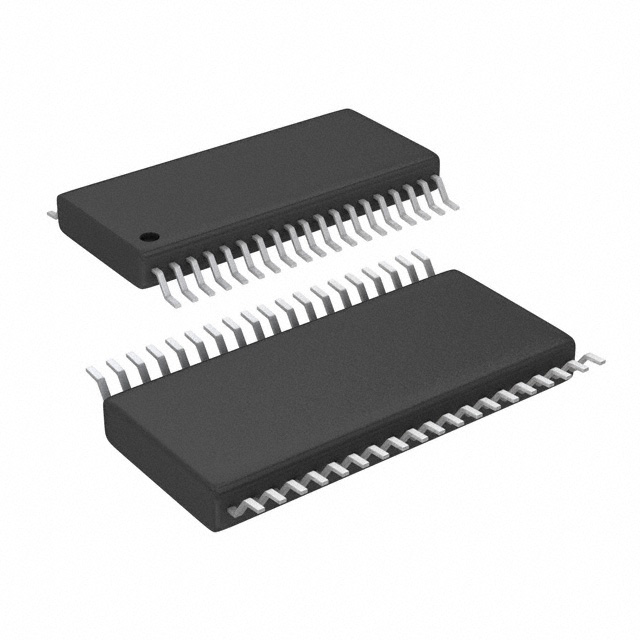


 工商网监
湘ICP备2023018690号
工商网监
湘ICP备2023018690号
