�������
�������
www.ti.com
SLUS479D − JANUARY 2001 − REVISED NOVEMBER 2004
�
��
��
�� ��� �
�����
��
��
�
� � � ��
� �
��
���
��� ���� �
�
�
�
� ���� �
�
�
FEATURES
DESCRIPTION
D Highly Integrated Solution With FET Pass
The bq2400x series ICs are advanced Li-Ion linear
charge management devices for highly integrated and
space-limited applications. They combine highaccuracy current and voltage regulation; FET passtransistor and reverse-blocking Schottky; battery
conditioning, temperature, or input-power monitoring;
charge termination; charge-status indication; and
charge timer in a small package.
Transistor and Reverse-Blocking Schottky
and Thermal Protection
D Timer-Enable Function That Allows Host to
Disable Charge Timer and Termination When
Charge Current Is Shared With a Load or
When Battery Is Absent
D Integrated Voltage and Current Regulation
With Programmable Charge Current
D High-Accuracy Voltage Regulation (±1%)
D Ideal for Low-Dropout Linear Charger
Designs for Single-Cell Li-Ion Packs With
Coke or Graphite Anodes
D Up to 1.2-A Continuous Charge Current
D Safety-Charge Timer During Preconditioning
and Fast Charge
D Integrated Cell Conditioning for Reviving
Deeply Discharged Cells and Minimizing Heat
Dissipation During Initial Stage of Charge
D Optional Temperature or Input-Power
Monitoring Before and During Charge
D Various Charge-Status Output Options for
Driving Single, Double, or Bicolor LEDs or
Host-Processor Interface
D Charge Termination by Minimum Current and
Time
D Low-Power Sleep Mode
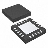
D Packaging: 5 mm × 5 mm MLP (bq24007)or
20-Lead TSSOP PowerPAD
APPLICATIONS
D
D
D
D
PDAs
Internet Appliances
MP3 Players
Digital Cameras
The bq24007 and bq24008 provide the timer-enable
function, allowing the host to disable the charge timer
when charge current is shared with a load or when the
battery is absent. This feature is ideal for applications
such as cellular phones, PDAs, and internet
appliances.
The bq2400x measures battery temperature using an
external thermistor. For safety reasons, the bq2400x
inhibits charge until the battery temperature is within the
user-defined thresholds. Alternatively, the user can
monitor the input voltage to qualify charge. The
bq2400x series then charge the battery in three phases:
preconditioning, constant current, and constant
voltage. If the battery voltage is below the internal
low-voltage threshold, the bq2400x uses low-current
precharge to condition the battery. A preconditioning
timer provides additional safety. Following preconditioning, the bq2400x applies a constant-charge
current to the battery. An external sense-resistor sets
the magnitude of the current. The constant-current
phase is maintained until the battery reaches the
charge-regulation voltage. The bq2400x then
transitions to the constant voltage phase. The user can
configure the device for cells with either coke or
graphite anodes. The accuracy of the voltage regulation
is better than ±1% over the operating junction
temperature and supply voltage range.
Charge is terminated by maximum time or minimum
taper current detection
The bq2400x automatically restarts the charge if the
battery voltage falls below an internal recharge
threshold.
Please be aware that an important notice concerning availability, standard warranty, and use in critical applications of Texas Instruments
semiconductor products and disclaimers thereto appears at the end of this data sheet.
PowerPAD is a trademark of Texas Instruments.
������� �
���� ���!"#$%�!� �� &'""(�% $� !� )'�*�&$%�!� +$%(, �"!+'&%�
&!��!"# %! �)(&���&$%�!�� )(" %-( %("#� !� �(.$� ��%"'#(�%� �%$�+$"+ /$""$�%0,
�"!+'&%�!� )"!&(����1 +!(� �!% �(&(��$"�*0 ��&*'+( %(�%��1 !� $** )$"$#(%("�,
Copyright 2002 − 2004, Texas Instruments Incorporated
��������
�������
www.ti.com
SLUS479D − JANUARY 2001 − REVISED NOVEMBER 2004
These devices have limited built-in ESD protection. The leads should be shorted together or the device placed in conductive foam during
storage or handling to prevent electrostatic damage to the MOS gates.
ORDERING INFORMATION
PACKAGE
TJ
CHARGE STATUS
CONFIGURATION
20-LEAD HTTSOP PowerPAD
(PWP)(1)
20-LEAD 5 mm × 5 mm MLP
(RGW)(2)
bq24007PWP
bq24007RGW
Single LED
bq24008PWP
Not available
Single bicolor LED
−40°C to 125°C
(1) The PWP package is available taped and reeled. Add R suffix to device type (e.g. bq24007PWPR) to order. Quantities 2500 devices per reel.
(2) The RGW package is available taped and reeled. Add R suffix to device type (e.g. bq24007RGWR) to order. Quantities 3000 devices per reel.
PACKAGE DISSIPATION RATINGS
PACKAGE
ΘJA
ΘJC
TA ≤ 25°C
POWER RATING
PWP(1)
RGW(2)
30.88°C/W
1.19°C/W
3.238 W
31.41°C/W
1.25°C/W
DERATING FACTOR
ABOVE TA = 25°C
0.0324W/°C
3.183 W
0.0318W/°C
(1) This data is based on using the JEDEC high-K board and topside traces, top and bottom thermal pad (6,5 × 3,4 mm), internal 1 oz power and
ground planes, 8 thermal via underneath the die connecting to ground plane.
(2) This data is based on using the JEDEC high-K board and topside traces, top and bottom thermal pad (3,25 × 3,25 mm), internal 1 oz power
and ground planes, 9 thermal via underneath the die connecting to ground plane.
ABSOLUTE MAXIMUM RATINGS
over operating free-air temperature range unless otherwise noted(1)
bq24007
bq24008
Supply voltage (VCC with respect to GND)
13.5 V
Input voltage (IN, ISNS, TMR EN, APG/THERM/CR/STAT1/STAT2, VSENSE, TMR SEL, VSEL) (all with respect to GND)
13.5 V
Output current (OUT pins)
2A
Output sink/source current (STAT1 and STAT2)
10 mA
Operating free-air temperature range, TA
−40°C to 70°C
Storage temperature range, Tstg
−65°C to 150°C
Junction temperature range, TJ
−40°C to 125°C
Lead temperature (Soldering, 10 s)
300°C
(1) Stresses beyond those listed under “absolute maximum ratings” may cause permanent damage to the device. These are stress ratings only, and
functional operation of the device at these or any other conditions beyond those indicated under “recommended operating conditions” is not
implied. Exposure to absolute-maximum-rated conditions for extended periods may affect device reliability.
RECOMMENDED OPERATING CONDITIONS
MIN
MAX
Supply voltage, VCC
4.5
10
V
Input voltage, VIN
4.5
10
V
Continuous output current
Operating junction temperature range, TJ
2
−40
UNIT
1.2
A
125
°C
��������
�������
www.ti.com
SLUS479D − JANUARY 2001 − REVISED NOVEMBER 2004
ELECTRICAL CHARACTERISTICS
over recommended operating junction temperature supply and input voltages, and VI (VCC) ≥ VI (IN) ( unless otherwise noted)
PARAMETER
VCC current
Standby current (sum of currents into OUT
and VSENSE pins)
TEST CONDITIONS
MIN
TYP
VCC > VCC_UVLO
VCC < VCC_UVLO,
VO(OUT) = 4.3 V,
VSENSE = 4.3 V
2
MAX
UNIT
1
mA
4
µA
VOLTAGE REGULATION, 0°C ≤ TJ ≤ 125°C
PARAMETER
TEST CONDITIONS
0 < IO ≤ 1.2 A
VSEL = VSS,
Output voltage
0 < IO ≤ 1.2 A
1 mA ≤ IO ≤ 1.2 A,
VI(IN)= 5 V,
VCC =5 V,
TJ = 25°C
VO(OUT)+VDO+Vilim(MAX) < VI(VCC) < 10 V,
VSEL = VCC,
Load regulation
Line regulation
Dropout voltage = VI(IN)-VO(OUT)
IO = 1.0 A,
IO = 1.2 A,
MIN
TYP
MAX
UNIT
4.059
4.10
4.141
V
4.158
4.20
4.242
V
TJ = 25°C
1
mV
0.01
%/V
4.9 V V(OVERV)?
Indicate Charge
No
No
VI(VSENSE) > V(OVERV)?
Yes
No
Yes
VI(VSENSE) < V(LOWV)?
No
VI(VSENSE) < V(LOWV)?
Yes
22.5 min Timer
Expired?
No
Yes
Fault Condition
Indicate Fault
POR?
or
APG/THERM Toggle?
No
Yes
Figure 15. Operational Flow Chart With the Charge Timers Disabled (TMR EN = 1)
Charge Qualification and Preconditioning
The bq2400x starts a charge cycle when power is applied
while a battery is present. Charge qualification is based on
battery voltage and the APG/THERM input.
As shown in the block diagram, the internal LowV
comparator output prevents fast-charging a deeply
depleted battery. When set, charging current is provided
by a dedicated precharge current source. The precharge
timer limits the precharge duration. The precharge current
also minimizes heat dissipation in the pass element during
the initial stage of charge.
The APG/THERM input can also be configured to monitor
14
either the adapter power or the battery temperature using
a thermistor. The bq2400x suspends charge if this input is
outside the limits set by the user. Please refer to the
APG/THERM input section for additional details.
Timer Enable Function
The logic TRM EN enables or disables the charge safety
timer. A low-level signal on this pin enables the timer
(charge and taper). A high-level input disables the timers
and allows the charger to operate continuously. No charge
termination is provided when this input is high. Note that
the preconditioning timer remains active regardless of the
status of this input.
The TRM EN input can be changed any time during the
charge cycle. A low-to-high transition on this pin resets the
timers.
��������
�������
www.ti.com
SLUS479D − JANUARY 2001 − REVISED NOVEMBER 2004
APG/THERM Input
The bq400x continuously monitors temperature or system
input voltage by measuring the voltage between the
APG/THERM (adapter power good/thermistor) and GND.
For temperature, a negative- or a positive- temperature
coefficient thermistor (NTC, PTC) and an external voltage
divider typically develop this voltage. (See Figure 16.) The
bq2400x compares this voltage against its internal VTP1
and VTP2 thresholds to determine if charging is allowed.
(See Figure 17.)
U1
1
N/C
2
IN
3
5
6
7
8
19
OUT
IN
4
20
N/C
OUT
VCC
VSENSE
ISNS
AGND
N/C
STAT2
APG/THM
STAT1
VSEL
10
−
16
PACK−
15
NTC Thermistor
14
13
TEMP
12
CR
GND
+
17
TMR EN TMR SEL
9
PACK+
18
Battery Pack
C3
0.22 µF
11
N/C
bq24008PWP
RT1
RT2
Figure 16. Temperature Sensing Circuit
If the charger designs incorporate a thermistor, the resistor
divider RT1 and RT2 is calculated by using the following
two equations.
Where:
First, calculate RT2.
RH = Resistance of the thermistor at the desired hot trip
threshold
V B RH R C
RT2 +
RH
ǒ
V
V
B
H
Ǔ
ƪ
1
V
C
*
* 1 * RC
ǒ
V
V
then use the resistor value to find RT1.
V
RT1 +
V
B
C
1
RT2
* 1
)
1
R
C
1
ƫ
V
H
B
C
Ǔ
* 1
VB = VCR (bias voltage)
RC = Resistance of the thermistor at the desired cold trip
threshold
VH = VP2 or the lower APG trip threshold
VC = VP2 or the upper APG trip threshold
RT1 = Top resistor in the divider string
RT2 = Bottom resistor in the divider string
15
��������
�������
www.ti.com
SLUS479D − JANUARY 2001 − REVISED NOVEMBER 2004
U1
VCC
1
2
DC+
3
VCC
4
Temp Fault
5
6
R1
VTP1
7
Normal Temp Range
VTP2
8
R2
9
Temp Fault
10
DC−
N/C
N/C
IN
OUT
IN
OUT
VCC
VSENSE
ISNS
AGND
N/C
STAT2
APG/THM
STAT1
TMR EN TMR SEL
VSEL
CR
GND
N/C
20
19
18
17
16
15
14
13
12
11
GND
bq24008PWP
Figure 17. Temperature Threshold
Figure 18. APG Sensing Circuit
Values of resistors R1 and R2 can be calculated using the following equation:
R2
V (APG) + VCC
(R1 ) R2)
where V(APG) is the voltage at the APG/THM pin.
Current Regulation
The bq2400x provides current regulation while the battery-pack voltage is less than the regulation voltage. The current
regulation loop effectively amplifies the error between a reference signal, Vilim, and the drop across the external sense
resistor, RSNS.
U1
VCC
1
R(SNS)
DC+
C1
10 µF
+
VCC
2
3
4
DC−
5
6
C2
0.1 µF
7
8
9
10
N/C
N/C
IN
OUT
IN
OUT
VCC
VSENSE
ISNS
AGND
N/C
STAT2
APG/THM
STAT1
TMR EN TMR SEL
VSEL
CR
GND
N/C
bq24008PWP
Figure 19. Current Sensing Circuit
16
20
19
18
17
16
15
14
13
12
11
��������
�������
www.ti.com
SLUS479D − JANUARY 2001 − REVISED NOVEMBER 2004
Charge current feedback, applied through pin ISNS,
maintains regulation around a threshold of Vilim. The
following formula calculates the value of the sense
resistor:
R (SNS) +
V(ilim)
Minimum Current: The bq2400x monitors the charging
current during the voltage regulation phase. The bq2400x
initiates a 22-minute timer once the current falls below the
taperdet trip threshold. Fast charge is terminated once the
22-minute timer expires.
Charge Status Display
I (REG)
where IREG is the desired charging current.
Voltage Monitoring and Regulation
Voltage regulation feedback is through pin VSENSE. This
input is tied directly to the positive side of the battery pack.
The bq2400x supports cells with either coke (4.1 V) or
graphite (4.2 V) anode. Pin VSEL selects the charge
regulation voltage.
The two available options allow the user to configure the
charge status display for single LED (bq24007) or a bicolor
LED (bq24008). The output stage is totem pole for the
bq24007 and bq24008. The following tables summarize
the operation of the three options:
Table 1. bq24007 (Single LED)
CHARGE STATE
STAT1
Precharge
ON (LOW)
Fast charge
ON (LOW)
VSEL State
(see Note)
CHARGE REGULATION
VOLTAGE
Low
4.1 V
Done (>90%)
OFF (HIGH)
High
4.2 V
Sleep-mode
OFF (HIGH)
APG/Therm invalid
OFF (HIGH)
Thermal shutdown
OFF (HIGH)
Battery absent
OFF (HIGH)
NOTE: VSEL should not be left floating.
Charge Termination
The bq2400x continues with the charge cycle until
termination by one of the two possible termination
conditions:
Maximum Charge Time: The bq2400x sets the maximum
charge time through pin TMRSEL. The TMR SEL pin
allows the user to select between three different total
charge-time timers (3, 4, 5, or 6 hours). The charge timer
is initiated after the preconditioning phase of the charge
and is reset at the beginning of a new charge cycle. Note
that in the case of a fault condition, such as an out-of-range
signal on the APG/THERM input or a thermal shutdown,
the bq2400x suspends the timer. Charge timers are active
only when TMR EN input is low.
TMRSEL STATE
Floating(1)
CHARGE TIME
Low
6 hours
High
4.5 hours
3 hours
(1) To improve noise immunity, it is recommended that a minimum of
10 pF capacitor be tied to Vss on a floating pin.
FAULT
Flashing (1 Hz, 50% duty cycle)
Table 2. bq24008 (Single Bicolor LED)
LED1 (RED)
LED2
(GREEN)
APPARENT
COLOR
Precharge
ON (LOW)
OFF (HIGH)
RED
Fast charge
ON (LOW)
OFF (HIGH)
RED
FAULT
ON (LOW)
ON (LOW)
YELLOW
CHARGE STATE
Done (>90%)
OFF (HIGH)
ON (LOW)
GREEN
Sleep-mode
OFF (HIGH)
OFF (HIGH)
OFF
APG/Therm
invalid
OFF (HIGH)
OFF (HIGH)
OFF
Thermal
shutdown
OFF (HIGH)
OFF (HIGH)
OFF
Battery absent
OFF (HIGH)
OFF (HIGH)(1)
OFF(1)
(1) If thermistor is used, then the green LED is off.
Thermal Shutdown
The bq2400x monitors the junction temperature TJ of the
DIE and suspends charging if TJ exceeds 165°C.
Charging resumes when TJ falls below 155°C.
17
��������
�������
www.ti.com
SLUS479D − JANUARY 2001 − REVISED NOVEMBER 2004
DETAILED DESCRIPTION
POWER FET
VOLTAGE SENSE
The integrated transistor is a P-channel MOSFET. The
power FET features a reverse-blocking Schottky diode,
which prevents current flow from OUT to IN.
To achieve maximum voltage regulation accuracy, the
bq2400x uses the feedback on the VSENSE pin.
Externally, this pin should be connected as close to the
battery cell terminals as possible. For additional safety, a
10-kΩ internal pullup resistor is connected between the
VSENSE and OUT pins.
An internal thermal-sense circuit shuts off the power FET
when the junction temperature rises to approximately
165°C. Hysteresis is built into the thermal sense circuit.
After the device has cooled approximately 10°C, the
power FET turns back on. The power FET continues to
cycle off and on until the fault is removed.
CURRENT SENSE
The bq2400x regulates current by sensing, on the ISNS
pin, the voltage drop developed across an external sense
resistor. The sense resistor must be placed between the
supply voltage (Vcc) and the input of the IC (IN pins).
18
TIMER ENABLE
The logic TMR EN enables or disables the charge safety
timer. A low-level signal on this pin enables the timers. A
high-level input disables the timers and allows the charge
to operate continuously. No charge termination is provided
when this input is high. Note that the preconditioning timer
remains active regardless of the status of this input.
��������
�������
www.ti.com
SLUS479D − JANUARY 2001 − REVISED NOVEMBER 2004
THERMAL INFORMATION
THERMALLY ENHANCED TSSOP-20
DIE
The thermally enhanced PWP package is based on the
20-pin TSSOP, but includes a thermal pad (see
Figure 20) to provide an effective thermal contact between
the IC and the PWB.
Traditionally, surface mount and power have been
mutually exclusive terms. A variety of scaled-down
TO220-type packages have leads formed as gull wings to
make them applicable for surface-mount applications.
These packages, however, suffer from several
shortcomings: they do not address the very low profile
requirements (< 2 mm) of many of today’s advanced
systems, and they do not offer a pin-count high enough to
accommodate increasing integration. On the other hand,
traditional low-power surface-mount packages require
power-dissipation derating that severely limits the usable
range of many high-performance analog circuits.
Side View (a)
DIE
End View (b)
Thermal
Pad
The PWP package (thermally enhanced TSSOP)
combines fine-pitch surface-mount technology with
thermal performance comparable to much larger power
packages.
The PWP package is designed to optimize the heat
transfer to the PWB. Because of the very small size and
limited mass of a TSSOP package, thermal enhancement
is achieved by improving the thermal conduction paths that
remove heat from the component. The thermal pad is
formed using a lead-frame design (patent pending) and
manufacturing technique to provide the user with direct
connection to the heat-generating IC. When this pad is
soldered or otherwise coupled to an external heat
dissipator, high power dissipation in the ultrathin, finepitch, surface-mount package can be reliably achieved.
Bottom View (c)
Figure 20. Views of Thermally Enhanced
PWP Package
Because the conduction path has been enhanced,
power-dissipation capability is determined by the thermal
considerations in the PWB design. For example, simply
adding a localized copper plane (heat-sink surface), which
is coupled to the thermal pad, enables the PWP package
to dissipate 2.5 W in free air. (Reference Figure 22(a), 8
cm2 of copper heat sink and natural convection.)
Increasing the heat-sink size increases the power
dissipation range for the component. The power
dissipation limit can be further improved by adding airflow
to a PWB/IC assembly. (See Figure 22(b) and 22(c).) The
line drawn at 0.3 cm2 in Figures 21 and 22 indicates
performance at the minimum recommended heat-sink
size.
19
��������
�������
www.ti.com
SLUS479D − JANUARY 2001 − REVISED NOVEMBER 2004
THERMAL INFORMATION
THERMAL RESISTANCE
vs
COPPER HEAT-SINK AREA
150
Natural Convection
R θ JA − Thermal Resistance −
° C/W
125
50 ft/min
100 ft/min
100
150 ft/min
200 ft/min
75
50
250 ft/min
300 ft/min
25
0 0.3
1
2
3
4
5
Copper Heat-Sink Area − cm2
Figure 21
20
6
7
8
��������
�������
www.ti.com
SLUS479D − JANUARY 2001 − REVISED NOVEMBER 2004
THERMAL INFORMATION
3.5
3.5
TA = 55°C
300 ft/min
PD − Power Dissipation Limit − W
3
150 ft/min
2.5
2
Natural Convection
1.5
1
0.5
0
3
300 ft/min
2.5
2
150 ft/min
1.5
Natural Convection
1
0.5
0
0.3
2
4
6
0
8
Copper Heat-Sink Size − cm2
0
0.3
2
4
6
Copper Heat-Sink Size − cm2
(a)
8
(b)
3.5
TA = 105°C
3
PD − Power Dissipation Limit − W
PD − Power Dissipation Limit − W
TA = 25°C
2.5
2
1.5
150 ft/min
300 ft/min
1
Natural Convection
0.5
0
0
0.3
2
4
6
8
Copper Heat-Sink Size − cm2
(c)
Figure 22. Power Ratings of the PWP Package at Ambient Temperatures of 25°C, 55°C, and 105°C
21
���IMPORTANT NOTICE
Texas Instruments Incorporated and its subsidiaries (TI) reserve the right to make corrections, modifications,
enhancements, improvements, and other changes to its products and services at any time and to discontinue
any product or service without notice. Customers should obtain the latest relevant information before placing
orders and should verify that such information is current and complete. All products are sold subject to TI’s terms
and conditions of sale supplied at the time of order acknowledgment.
TI warrants performance of its hardware products to the specifications applicable at the time of sale in
accordance with TI’s standard warranty. Testing and other quality control techniques are used to the extent TI
deems necessary to support this warranty. Except where mandated by government requirements, testing of all
parameters of each product is not necessarily performed.
TI assumes no liability for applications assistance or customer product design. Customers are responsible for
their products and applications using TI components. To minimize the risks associated with customer products
and applications, customers should provide adequate design and operating safeguards.
TI does not warrant or represent that any license, either express or implied, is granted under any TI patent right,
copyright, mask work right, or other TI intellectual property right relating to any combination, machine, or process
in which TI products or services are used. Information published by TI regarding third-party products or services
does not constitute a license from TI to use such products or services or a warranty or endorsement thereof.
Use of such information may require a license from a third party under the patents or other intellectual property
of the third party, or a license from TI under the patents or other intellectual property of TI.
Reproduction of information in TI data books or data sheets is permissible only if reproduction is without
alteration and is accompanied by all associated warranties, conditions, limitations, and notices. Reproduction
of this information with alteration is an unfair and deceptive business practice. TI is not responsible or liable for
such altered documentation.
Resale of TI products or services with statements different from or beyond the parameters stated by TI for that
product or service voids all express and any implied warranties for the associated TI product or service and
is an unfair and deceptive business practice. TI is not responsible or liable for any such statements.
Following are URLs where you can obtain information on other Texas Instruments products and application
solutions:
Products
Applications
Amplifiers
amplifier.ti.com
Audio
www.ti.com/audio
Data Converters
dataconverter.ti.com
Automotive
www.ti.com/automotive
DSP
dsp.ti.com
Broadband
www.ti.com/broadband
Interface
interface.ti.com
Digital Control
www.ti.com/digitalcontrol
Logic
logic.ti.com
Military
www.ti.com/military
Power Mgmt
power.ti.com
Optical Networking
www.ti.com/opticalnetwork
Microcontrollers
microcontroller.ti.com
Security
www.ti.com/security
Telephony
www.ti.com/telephony
Video & Imaging
www.ti.com/video
Wireless
www.ti.com/wireless
Mailing Address:
Texas Instruments
Post Office Box 655303 Dallas, Texas 75265
Copyright 2004, Texas Instruments Incorporated
�