bq24020,, bq24022,, bq24023
bq24024, bq24025, bq24026
bq24027
www.ti.com
SLUS549E – DECEMBER 2002 – REVISED NOVEMBER 2007
SINGLE-CHIP, LI-ION AND LI-POL CHARGER IC WITH AUTONOMOUS USB-PORT AND
AC-ADAPTER SUPPLY MANAGEMENT (bqTINY™-II)
FEATURES
1
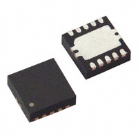
• Small 3 mm × 3 mm MLP Package
• Charges and powers Systems from Either AC
Adapter or USB With Autonomous
power-Source Selection
• Integrated USB Control With Selectable 100
mA and 500 mA Charge Rates
• Ideal for Low-Dropout Charger Designs for
Single-Cell Li-Ion or Li-pol Packs in Space
Limited portable applications
• Integrated power FET and Current Sensor for
Up to 1-A Charge applications From AC
Adapter
• Precharge Conditioning With Safety Timer
• power Good (AC Adapter Present) Status
Output
• Optional Battery Temperature Monitoring
Before and During Charge
• Automatic Sleep Mode for Low-power
Consumption
2
APPLICATIONS
•
•
•
•
PDAs, MP3 Players
Digital Cameras
Internet appliances
Smartphones
VDC
AC
ADAPTER
DESCRIPTION
The bqTINY-II series are highly-integrated, flexible
Li-Ion linear charge and system power management
devices for space-limited charger applications. In a
single monolithic device, the bqTINY-II offers
integrated
USB-port
and
ac-adapter
supply
management
with
autonomous
power-source
selection, power-FET and current-sensor interfaces,
high-accuracy current and voltage regulation, charge
status, and charge termination.
The bqTINY-II automatically selects the USB-port or
the ac-adapter as the power source for the system. In
the USB configuration, the host can select from two
preset charge rates of 100 mA or 500 mA. In the
ac-adapter configuration, an external resistor sets the
system or charge current.
The bqTINY-II charges the battery in three phases:
conditioning, constant current, and constant voltage.
Charge is terminated based on minimum current. An
internal charge timer provides a backup safety for
charge termination. The bqTINY-II automatically
restarts the charge if the battery voltage falls below
an internal threshold. The bqTINY-II automatically
enters sleep mode when both supplies are removed.
PACK+
bq24020DRC
1
AC
OUT
+
10
GND
VBUS
USB
PORT
GND
BATTERY PACK
SYSTEM
PACK−
2
USB
TS
9
3
STAT1
CE
8
4
STAT2 ISET2
7
5
VSS
6
SYSTEM
INTERFACE
RSET
ISET1
D+
UDG−02184
D−
1
2
Please be aware that an important notice concerning availability, standard warranty, and use in critical applications of
Texas Instruments semiconductor products and disclaimers thereto appears at the end of this data sheet.
bqTINY is a trademark of Texas Instruments.
PRODUCTION DATA information is current as of publication date.
Products conform to specifications per the terms of the Texas
Instruments standard warranty. Production processing does not
necessarily include testing of all parameters.
Copyright © 2002–2007, Texas Instruments Incorporated
�bq24020,, bq24022,, bq24023
bq24024, bq24025, bq24026
bq24027
www.ti.com
SLUS549E – DECEMBER 2002 – REVISED NOVEMBER 2007
These devices have limited built-in ESD protection. The leads should be shorted together or the device placed in conductive foam
during storage or handling to prevent electrostatic damage to the MOS gates.
DESCRIPTION CONTINUED
Different versions of the bqTINY-II offer many additional features. These include a temperature-sensor input for
detecting hot or cold battery packs, a power-good output (PG) indicating the presence of input power, a TTL-level
charge-enable input (CE) used to disable or enable the charge process, and a TTL-level timer and taper-detect
enable input (TTE) used to disable or enable the fast-charge timer and charge termination.
ORDERING INFORMATION
CHARGE
REGULATION
VOLTAGE (V)(1)
TJ
– 40°C
to
125°C
(1)
OPTIONAL
FUNCTIONS (1)
FAST-CHARGE
TIMER (Hours)
TAPER
TIMER
USB TAPER
THRESHOLD
PART
NUMBER(2)
4.2
CE and TS
5
Yes
10% of ISET1 Level
bq24020DRCR
AZS
4.2
PG and CE
5
Yes
10% of ISET1 Level
bq24022DRCR
AZU
4.2
CE and TTE
5
Yes
10% of ISET1 Level
bq24023DRCR
AZV
4.2
TTE and TS
5
Yes
10% of ISET1 Level
bq24024DRCR
AZW
4.2
CE and TS
7
Yes
10% of ISET1 Level
bq24025DRCR
AZX
bq24026DRCR
ANR
bq24027DRCR
ANS
4.2
TE and TS
7
No
10% of selected
USB charge rate
4.2
PG and CE
7
No
10% of selected
USB charge rate
MARKINGS
The DRC package is available taped and reeled only in quantities of 3,000 devices per reel.
Dissipation Ratings
(1)
PACKAGE
θJA
TA < 40°C POWER RATING
DERATING FACTOR ABOVE TA = 25°C
DRC (1)
46.87 °C/W
1.5 W
0.021 W/°C
This data is based on using the JEDEC High-K board and the exposed die pad is connected to a copper pad on the board. This is
connected to the ground plane by a 2×3 via matrix.
ABSOLUTE MAXIMUM RATINGS (1)
over operating free-air temperature range (unless otherwise noted)
bq24020, bq24022,
bq24023, bq24024
bq24025, bq24026
bq24027
UNIT
Input voltage (2)
AC, CE, ISET1, ISET2, OUT, PG, STAT1, STAT2, TE, TS, TTE, USB
–0.3 to 7.0
V
Output sink/source current
STAT1, STAT2, PG
15
mA
Output current
TS
200
µA
Output current
OUT
1.5
A
Operating free-air temperature range, TA
Junction temperature range, TJ
Storage temperature, Tstg
(1)
(2)
2
–40 to 125
°C
–65 to 150
Stresses beyond those listed under "absolute maximum ratings" may cause permanent damage to the device. These are stress ratings
only, and functional operation of the device at these or any other conditions beyond those indicated under "recommended operating
conditions" is not implied. Exposure to absolute-maximum-rated conditions for extended periods may affect device reliability.
All voltages are with respect to VSS.
Submit Documentation Feedback
Copyright © 2002–2007, Texas Instruments Incorporated
Product Folder Link(s): bq24020 bq24022 bq24023 bq24024 bq24025 bq24026 bq24027
�bq24020,, bq24022,, bq24023
bq24024, bq24025, bq24026
bq24027
www.ti.com
SLUS549E – DECEMBER 2002 – REVISED NOVEMBER 2007
RECOMMENDED OPERATING CONDITIONS
over operating free-air temperature range (unless otherwise noted)
MIN
Supply voltage (from AC input), VCC
NOM
MAX
UNIT
4.5
6.5
V
Supply voltage (from USB input), VCC
4.35
6.5
V
Operating junction temperature range, TJ
–40
125
°C
ELECTRICAL CHARACTERISTICS
over 0°C ≤ TJ ≤ 125°C and recommended supply voltage, unless otherwise noted
PARAMETER
TEST CONDITIONS
MIN
TYP
MAX
1.2
2.0
UNIT
INPUT CURRENT
ICC(VCC)
VCC current
VCC > VCC(min)
ICC(SLP)
Sleep current
Sum of currents into OUT pin, VCC < V(SLP)
ICC(STBY)
Standby current
CE = High
0°C ≤TJ ≤ 85°C
IIB(OUT)
Input current on OUT pin
Charge DONE
VCC > VCC(MIN)
IIB(CE)
Input current on CE pin
1
IIB(TTE)
Input bias current on TTE pin
1
IIB(TE)
Input bias current on TE pin
1
2
5
1
150
5
mA
µA
VOLTAGE REGULATION VO(REG) + V(DO-MAX) ≤ VCC , I(TERM) < IO(OUT) ≤ 1 A
VO(REG)
Output voltage,
4.20
Voltage regulation accuracy
V(DO)
AC dropout voltage (V(AC)–V(OUT))
V(DO)
USB dropout voltage
(V(USB) – V(OUT))
TA = 25°C
V
–0.35%
0.35%
–1%
1%
VO(OUT) = VO(REG)
VO(REG) + V(DO-MAX)) ≤ VCC
IO(OUT) = 1A
350
500
VO(OUT) = VO(REG)
VO(REG) + V(DO-MAX)) ≤ VCC
ISET2 = High
350
500
VO(OUT) = VO(REG)
VO(REG) + V(DO-MAX)) ≤ VCC
ISET2 = Low
60
100
VI(OUT) > V(LOWV)
VI(AC) – VI(OUT) > V(DO-MAX)
VCC ≥ 4.5 V
50
1000
VCC(MIN) ≥ 4.5 V
VUSB – VI(OUT) > V(DO-MAX)
VI(OUT) > V(LOWV)
ISET2 = Low
80
100
VCC(MIN) ≥ 4.5 V
VUSB – VI(OUT) > V(DO-MAX)
VI(OUT) > V(LOWV)
ISET2 = High
400
500
mV
CURRENT REGULATION
IO(OUT)
AC output current range (1)
IO(OUT)
USB output current range
V(SET)
Output current set voltage
K(SET)
(1)
Output current set factor
IO(OUT) +
ǒK(SET)
Voltage on ISET1 pin, VCC ≥ 4.5 V, VIN ≥ 4.5 V,
VI(OUT) > V(LOWV), VIN – VI(OUT) > V(DO-MAX)
2.463
2.500
2.538
50 mA ≤ IO(OUT) ≤ 1 A
307
322
337
10 mA ≤ IO(OUT) < 50 mA
296
320
346
1 mA ≤ IO(OUT) < 10 mA
246
320
416
mA
V
Ǔ
V(SET)
RSET
Copyright © 2002–2007, Texas Instruments Incorporated
Submit Documentation Feedback
Product Folder Link(s): bq24020 bq24022 bq24023 bq24024 bq24025 bq24026 bq24027
3
�bq24020,, bq24022,, bq24023
bq24024, bq24025, bq24026
bq24027
www.ti.com
SLUS549E – DECEMBER 2002 – REVISED NOVEMBER 2007
ELECTRICAL CHARACTERISTICS (continued)
over 0°C ≤ TJ ≤ 125°C and recommended supply voltage, unless otherwise noted
PARAMETER
TEST CONDITIONS
MIN
TYP
MAX
UNIT
PRECHARGE AND SHORT-CIRCUIT CURRENT REGULATION
V(LOWV)
Precharge to fast-charge
transition threshold
Voltage on OUT pin
2.8
3.0
3.2
Deglitch time for fast-charge to
precharge transition
VCC(MIN) ≥ 4.5 V, tFALL = 100 ns, 10 mV
overdrive, VI(OUT) decreasing below threshold
250
375
500
(2)
IO(PRECHG)
Precharge range
0 V < VI(OUT) < V(LOWV), t < t(PRECHG)
V(PRECHG)
Precharge set voltage
Voltage on ISET1 pin
0 V < VI(OUT) > V(LOWV),
5
VO(REG) = 4.2 V
t < t(PRECHG)
100
240
255
270
V
ms
mA
mV
CHARGE TAPER AND TERMINATION DETECTION
I(TAPER)
Charge taper detection range (3)
VI(OUT) > V(RCH), t < t(TAPER)
USB-100 charge taper
detection level
bq24026
VI(OUT) > V(RCH), ISET2 = Low
USB-500 charge taper
detection level
bq24026
VI(OUT) > V(RCH), ISET2 = High
5
100
6.5
9
11
mA
32
44
55
V(TAPER)
Charge taper detection set voltage
Voltage on ISET1 pin, VO(REG) = 4.2 V,
VI(OUT) > V(RCH), t < t(TAPER)
235
250
265
V(TERM)
Charge termination detection
set voltage (4)
Voltage on ISET1 pin, VO(REG) = 4.2 V,
VI(OUT) > V(RCH)
11
18
25
375
500
Deglitch time for TAPER detection
VCC(MIN) ≥ 4.5 V, tFALL = 100 ns charging
current increasing or decreasing above and
below, 10 mV overdrive
250
t(TPRDET)
t(TRMDET)
Deglitch time for
termination detection
VCC(MIN) ≥ 4.5 V, tFALL = 100 ns charging
current decreasing below, 10 mV overdrive
250
375
500
mV
ms
TEMPERATURE SENSE COMPARATOR
V(HTF)
High-voltage threshold
PTC thermistor
2.475
2.500
2.525
V(LTF)
Low-voltage threshold
PTC thermistor
0.485
0.500
0.515
I(TS)
Current source
96
102
108
µA
t(DEGL)
Deglitch time for temperature fault
250
375
500
ms
(2)
(3)
(4)
4
IO(PRECHG) +
IO(TAPER) +
IO(TERM) +
V
Ǔ
ǒK(SET)
V(PRECHG)
RSET
ǒK(SET)
Ǔ
V(TAPER)
R SET
ǒK(SET)
Ǔ
V(TERM)
RSET
Submit Documentation Feedback
Copyright © 2002–2007, Texas Instruments Incorporated
Product Folder Link(s): bq24020 bq24022 bq24023 bq24024 bq24025 bq24026 bq24027
�bq24020,, bq24022,, bq24023
bq24024, bq24025, bq24026
bq24027
www.ti.com
SLUS549E – DECEMBER 2002 – REVISED NOVEMBER 2007
ELECTRICAL CHARACTERISTICS (continued)
over 0°C ≤ TJ ≤ 125°C and recommended supply voltage, unless otherwise noted
PARAMETER
TEST CONDITIONS
MIN
TYP
MAX
UNIT
VO(REG)
– 0.115
VO(REG)
–0.10
VO(REG)
– 0.085
250
375
500
ms
0.25
V
BATTERY RECHARGE THRESHOLD
VRCH
Recharge threshold
t(DEGL)
Deglitch time for recharge detect
VCC(MIN) ≥ 4.5 V, tFALL = 100 ns decreasing
below or increasing above threshold,
10 mV overdrive
V
STAT1, STAT2, and PG OUTPUTS
VOL
Low-level output saturation voltage IO = 5 mA
ISET2, CHARGE ENABLE (CE), TIMER AND TERMINATION ENABLE (TTE), AND TIMER ENABLE (TE) INPUTS
VIL
Low-level input voltage
IIL = 10 µA
0
VIH
High-level input voltage
IIL = 20 µA
1.4
IIL
CE, TE or TTE low-level
input current
IIH
CE, TE or TTE high-level
input current
IIL
ISET2 low-level input current
IISET2 = 0
IIH
ISET2 high-level input current
IISET2 = VCC
IIH
ISET2 high-Z input current
0.4
V
–1
1
µA
–20
40
1
V
TIMERS
t(PRECHG)
t(TAPER)
t(CHG)
I(FAULT)
Precharge time
bq24020
bq24022
bq24023
bq24024
bq24025
Taper time
Charge time
1,584
1,800
2,016
1,584
1,800
2,016
s
bq24020
bq24022
bq24023
bq24024
15,840
18,000
20,160
bq24025
bq24026
bq24027
22,176
25,200
28,224
Timer fault recovery current
µA
200
SLEEP COMPARATOR
V(SLP)
Sleep-mode entry
threshold voltage
V(SLPEXIT)
Sleep mode exit
threshold voltage
2.3 V ≤ VI(OUT) ≤ VO(REG)
Sleep mode deglitch time
AC and USB decreasing below threshold,
tFALL = 100 ns, 10 mV overdrive
VCC ≤
VI(OUT)
+80 mV
2.3 V ≤ VI(OUT) ≤ VO(REG)
VCC ≥
VI(OUT)
+190mV
250
375
500
V
ms
THERMAL SHUTDOWN THRESHOLDS
T(SHTDWN)
Thermal trip threshold
165
Thermal hysteresis
°C
15
UNDERVOLTAGE LOCKOUT
V(UVLO)
Undervoltage lockout
Decreasing VCC
2.4
Hysteresis
2.5
2.6
27
Copyright © 2002–2007, Texas Instruments Incorporated
Submit Documentation Feedback
Product Folder Link(s): bq24020 bq24022 bq24023 bq24024 bq24025 bq24026 bq24027
V
mV
5
�bq24020,, bq24022,, bq24023
bq24024, bq24025, bq24026
bq24027
www.ti.com
SLUS549E – DECEMBER 2002 – REVISED NOVEMBER 2007
DRC PACKAGE
(TOP VIEW)
VSS STAT2 STAT1 USB
5
4
3
2
AC
1
DRC PACKAGE
(TOP VIEW)
VSS STAT2 STAT1 USB
5
bq24020DRC
bq24025DRC
6
7
ISET1 ISET2 CE
10
TS
OUT
DRC PACKAGE
(TOP VIEW)
VSS STAT2 STAT1 USB
5
4
3
3
2
1
bq24022DRC
9
8
4
AC
2
6
7
8
ISET1 ISET2 PG
9
10
CE
OUT
DRC PACKAGE
(TOP VIEW)
AC
1
VSS STAT2 STAT1 USB
5
4
3
2
AC
1
bq24023DRC
bq24024DRC
6
7
8
ISET1 ISET2 CE
9
10
TTE OUT
6
5
4
3
2
7
8
ISET1 ISET2 TE
6
Submit Documentation Feedback
9
10
TS
OUT
DRC PACKAGE
(TOP VIEW)
AC
1
VSS STAT2 STAT1 USB
5
bq24026DRC
6
8
ISET1 ISET2 TTE
DRC PACKAGE
(TOP VIEW)
VSS STAT2 STAT1 USB
7
4
3
AC
2
1
9
10
CE
OUT
bq24027DRC
9
10
TS
OUT
6
7
8
ISET1 ISET2 PG
Copyright © 2002–2007, Texas Instruments Incorporated
Product Folder Link(s): bq24020 bq24022 bq24023 bq24024 bq24025 bq24026 bq24027
�bq24020,, bq24022,, bq24023
bq24024, bq24025, bq24026
bq24027
www.ti.com
SLUS549E – DECEMBER 2002 – REVISED NOVEMBER 2007
Terminal Functions
TERMINAL
NAME
I/O
bq24020 bq24022
bq24023 bq24024 bq24026
bq24025 bq24027
DESCRIPTION
AC
1
1
1
1
1
I
AC charge input voltage
CE
8
9
8
-
-
I
Charge enable input (active low)
ISET1
6
6
6
6
6
I
Charge current set point for AC input and precharge and taper
set point for both AC and USB
ISET2
7
7
7
7
7
I
Charge current set point for USB port (high=500 mA, low=100
mA, hi-z = disable USB charge)
OUT
10
10
10
10
10
O
Charge current output
PG
-
8
-
-
-
O
powergood status output (active low)
STAT1
3
3
3
3
3
O
Charge status output 1 (open-drain)
STAT2
4
4
4
4
4
O
Charge status output 2 (open-drain)
TE
-
-
-
-
8
I
Timer enable input (active low)
TS
9
-
-
9
9
I
Temperature sense input
TTE
-
-
9
8
-
I
Timer and termination enable input (active low)
USB
2
2
2
2
2
I
USB charge input voltage
VSS
5
5
5
5
5
-
Ground input
-
There is an internal electrical connection between the exposed
thermal pad and VSS pin of the device. The exposed thermal
pad must be connected to the same potential as the VSS pin
on the printed circuit board. Do not use the thermal pad as
the primary ground input for the device. VSS pin must be
connected to ground at all times
Exposed
Thermal
Pad
pad
pad
pad
pad
Copyright © 2002–2007, Texas Instruments Incorporated
pad
Submit Documentation Feedback
Product Folder Link(s): bq24020 bq24022 bq24023 bq24024 bq24025 bq24026 bq24027
7
�bq24020,, bq24022,, bq24023
bq24024, bq24025, bq24026
bq24027
www.ti.com
SLUS549E – DECEMBER 2002 – REVISED NOVEMBER 2007
FUNCTIONAL BLOCK DIAGRAM
AC
USB
VI(AC)
AC
VI(OUT)
VI(REG)
VI(USB)
VI(OUT)
+
VI(ISET)
sensefet
VI(SET)
REF
BIAS
AND
UVLO
OUT
ISET1
+
USB
AC/USB
V(SET)
VI(ISET-USB)
CHG
ENABLE
AC/USB
sensefet
VO(REG)
sensefet
UVLO
V(HTF)
VI(ISET-USB)
100 mA/500 mA
*
I(TS)
SUSPEND
THERMAL
SHUTDOWN
TS
AC/USB
CHG ENABLE
*
V(LTF)
500 mA/ 100 mA
CE
VI(OUT)
*
SLEEP (AC)
*
SLEEP (USB)
VBAT
ISET1
VI(AC)
VI(OUT)
TTE
OR
TE
VI(USB)
VO(REG)
VI(OUT)
RECHARGE
*
VI(OUT)
*
CHARGE
CONTROL,
TIMER,
AND
DISPLAY
LOGIC
PRECHARGE
(C/10)
500 mA/ 100 mA
ISET2
USB CHARGE
PG
PRECHARGE
VI(SET)
VI(SET)
*
VI(SET)
t(TAPER) TIMER
*
TAPER
STAT1
TERM
STAT2
VSS
* SIGNAL DEGLITCHED
8
Submit Documentation Feedback
UDG−02185
Copyright © 2002–2007, Texas Instruments Incorporated
Product Folder Link(s): bq24020 bq24022 bq24023 bq24024 bq24025 bq24026 bq24027
�bq24020,, bq24022,, bq24023
bq24024, bq24025, bq24026
bq24027
www.ti.com
SLUS549E – DECEMBER 2002 – REVISED NOVEMBER 2007
TYPICAL CHARACTERISTICS
AC DROPOUT VOLTAGE
vs
JUNCTION TEMPERATURE
450
IO(OUT) = 1000 mA
400
Dropout Voltage − mV
350
IO(OUT) = 750 mA
300
250
IO(OUT) = 500 mA
200
150
IO(OUT) = 250 mA
100
50
0
0
50
100
TJ − Junction Temperature − _C
Figure 1.
150
The bqTINY-II supports a precision Li-Ion, Li-pol charging system suitable for single-cell packs. Figure 3 shows a
typical charge profile, application circuit and Figure 4 shows an operational flow chart.
Regulation
Voltage
Pre-Conditioning
Phase
Voltage Regulation
and Charge Termination Phase
Current Regulation
Phase
Regulation
Current
Charge
Voltage
Minimum
Charge
Voltage
Charge
Complete
Charge
Current
Pre-Conditioning
and Taper Detect
t(PRECHG)
t(CHG)
Figure 2. Typical Charging Profile
Copyright © 2002–2007, Texas Instruments Incorporated
Submit Documentation Feedback
Product Folder Link(s): bq24020 bq24022 bq24023 bq24024 bq24025 bq24026 bq24027
9
�bq24020,, bq24022,, bq24023
bq24024, bq24025, bq24026
bq24027
www.ti.com
SLUS549E – DECEMBER 2002 – REVISED NOVEMBER 2007
FUNCTIONAL DESCRIPTION
AC ADAPTER
VDC
bq24023DRC
1
AC
0.1 µF
GND
D+
D−
VBUS
PACK+
OUT 10
SYSTEM
+
SYSTEM
INTERFACE
PACK−
2
USB
TTE
9
3
STAT1
CE
8
4
STAT2 ISET2 7
5
VSS
GND
USB PORT
ISET1 6
RSET
UDG−02184
Figure 3. Typical Application Circuit
10
Submit Documentation Feedback
Copyright © 2002–2007, Texas Instruments Incorporated
Product Folder Link(s): bq24020 bq24022 bq24023 bq24024 bq24025 bq24026 bq24027
�bq24020,, bq24022,, bq24023
bq24024, bq24025, bq24026
bq24027
www.ti.com
SLUS549E – DECEMBER 2002 – REVISED NOVEMBER 2007
POR
SLEEP MODE
Vcc > VI(OUT)
checked at all times
No
Indicate SLEEP
MODE
Yes
VI(OUT) BATTERY
AC MODE
USB MODE
AC < BATTERY
USB > BATTERY
UDG−02187
Figure 5. Typical Charging Profile
TEMPERATURE QUALIFICATION (bq24020, bq24024, bq24025, and bq24026 only)
The bqTINY-II continuously monitors battery temperature by measuring the voltage between the TS and VSS
pins. An internal current source provides the bias for common 10-kΩ negative-temperature coefficient thermistors
(NTC) (see Figure 6). The device compares the voltage on the TS pin with the internal V(LTF) and V(HTF)
thresholds to determine if charging is allowed. If a temperature outside the V(LTF) and V(HTF) thresholds is
detected, the device immediately suspends the charge by turning off the power FET and holding the timer value
(i.e. timers are NOT reset). Charge is resumed when the temperature returns within the normal range.
The allowed temperature range for a 103AT-type thermistor is 0°C to 45°C. However the user may modify these
thresholds by adding two external resistors. See Figure 7.
BATTERY PRE-CONDITIONING
If the battery voltage falls below the V(LOWV) threshold during a charge cycle, the bqTINY-II applies a precharge
current, IO(PRECHG), to the battery. This feature revives deeply discharged cells. The resistor connected between
the ISET1 and VSS, RSET, determines the precharge rate. The V(PRECHG) and K(SET) parameters are specified in
the specifications table. Note that this applies to both AC and USB charging.
V (PRECGH) K (SET)
I O (PRECHG)
RSET
(1)
The bqTINY-II activates a safety timer, t(PRECHG), during the conditioning phase. If V(LOWV) threshold is not
reached within the timer period, the bqTINY-II turns off the charger and asserts a FAULT code on the STATx
pins. Please refer to the TIMER FAULT RECOVERY section for additional details.
PACK+
bqTINYII
TS
LTF
HTF
9
TEMP
VHTF
PACK−
TS
NTC
BATTERY
PACK
VLTF
+
ITS
PACK−
ITS
PACK+
bqTINYII
+
LTF
RT1
9
VLTF
RT2
HTF
12
Submit Documentation Feedback
NTC
BATTERY
PACK
VHTF
UDG−02188
UDG−02186
Figure 6. Temperature Sensing Configuration
TEMP
Figure 7. Temperature Sensing Thresholds
Copyright © 2002–2007, Texas Instruments Incorporated
Product Folder Link(s): bq24020 bq24022 bq24023 bq24024 bq24025 bq24026 bq24027
�bq24020,, bq24022,, bq24023
bq24024, bq24025, bq24026
bq24027
www.ti.com
SLUS549E – DECEMBER 2002 – REVISED NOVEMBER 2007
BATTERY CHARGE CURRENT
The bqTINY-II offers on-chip current regulation with a programmable set point. The resistor connected between
the ISET1 and VSS, RSET, determines the AC charge rate. The V(SET) and K(SET) parameters are specified in the
specifications table.
IO(OUT) +
ǒK(SET)
Ǔ
V(SET)
RSET
(2)
When charging from a USB port, the host controller has the option of selecting either a 100-mA or a 500-mA
charge rate using the ISET2 pin. A low-level signal sets the current at 100 mA, and a high-level signal sets the
current at 500 mA. A high-Z input disables USB charging
BATTERY VOLTAGE REGULATION
The voltage regulation feedback is through the OUT pin. This input is tied directly to the positive side of the
battery pack. The bqTINY-II monitors the battery-pack voltage between the OUT and VSS pins. When the battery
voltage rises to the VO(REG) threshold, the voltage-regulation phase begins and the charging current begins to
taper down.
As a safety backup, the bqTINY-II also monitors the charge time. If the charge is not terminated within the time
period specified by t(CHG), the bqTINY-II turns off the charger and asserts a FAULT code on the STATx pins.
Please refer to the TIMER FAULT RECOVERY section for additional details.
CHARGE TAPER DETECTION, TERMINATION AND RECHARGE
The bqTINY-II monitors the charging current during the voltage-regulation phase. When the taper threshold,
I(TAPER), is detected, the bqTINY-II initiates the taper timer, t(TAPER). Charge is terminated after the timer expires.
The resistor connected between the ISET1 and VSS, RSET, determines the taper detection level. The V(TAPER) and
K(SET) parameters are specified in the specifications table. Note that this applies to both AC and USB charging.
V(TAPER) K(SET)
I (TAPER) +
RSET
(3)
The bqTINY-II resets the taper timer if the charge current rises above the taper threshold, I(TAPER).
In addition to taper-current detection, the bqTINY-II terminates charge if the charge current falls below the I(TERM)
threshold. This feature allows quick recognition of a battery-removal condition, or insertion of a fully charged
battery. Note that the charge timer and taper timer are bypassed for this feature. The resistor connected between
the ISET1 and VSS, RSET, determines the taper detection level. The V(TERM) and K(SET) parameters are specified in
the specifications table. Note that this applies to both AC and USB charging.
V(TERM) K(SET)
I (TERM) +
R SET
(4)
After charge termination, the bqTINY-II re-starts the charge when the voltage on the OUT pin falls below the
V(RCH) threshold. This feature keeps the battery at full capacity at all times.
Note ON bq24026 AND bq24027
The bq24026 and bq24027 monitor the charging current during the voltage-regulation phase. Once the taper
threshold, I(TAPER), is detected, the bq24026/27 terminates the charge. There is no taper timer (t(TAPER)) for this
version.
The resistor connected between the ISET1 and VSS, RSET, determines the taper-detect level for AC input. For
USB charge, taper level is fixed at 10% of the 100- or 500-mA charge rate.
Also note that there is I(TERM) detection in the bq24026 and the bq24027.
SLEEP MODE
The bqTINY-II enters low-power sleep mode if both AC and USB are removed from the circuit. This feature
prevents draining the battery in the absence of input supply.
Copyright © 2002–2007, Texas Instruments Incorporated
Submit Documentation Feedback
Product Folder Link(s): bq24020 bq24022 bq24023 bq24024 bq24025 bq24026 bq24027
13
�bq24020,, bq24022,, bq24023
bq24024, bq24025, bq24026
bq24027
www.ti.com
SLUS549E – DECEMBER 2002 – REVISED NOVEMBER 2007
CHARGE STATUS OUTPUTS
The open-drain STAT1 and STAT2 outputs indicate various charger operations as shown in the following table.
These status pins can be used to drive LEDs or communicate to the host processor. Note that OFF indicates the
open-drain transistor is turned off.
Table 1. Status Pins Summary (1)
CHARGE STATE
STAT1
STAT2
Precharge in progress
ON
ON
Fast charge in progress
ON
OFF
Charge done
OFF
ON
Charge suspend (temperature)
OFF
OFF
Timer fault
OFF
OFF
Sleep mode
OFF
OFF
(1)
OFF means the open-drain output transistor on the STAT1 and STAT2 pins is in an off state.
PG OUTPUT
The open-drain PG (power Good) indicates when the AC adapter is present. The output turns ON when a valid
voltage is detected. This output is turned off in the sleep mode. The PG pin can be used to drive an LED or to
communicate to the host processor.
CE INPUT (CHARGE ENABLE)
The CE digital input is used to disable or enable the charge process. A low-level signal on this pin enables the
charge. A high-level signal disables the charge, and places the device in a low-power mode. A high-to-low
transition on this pin also resets all timers and timer fault conditions. Note that this applies to both AC and USB
charging.
TTE INPUT (TIMER AND TERMINATION ENABLE)
The TTE digital input is used to disable or enable the fast-charge timer and charge-taper detection. A low-level
signal on this pin enables the fast-charge timer and taper timer, and a high-level signal disables this feature.
Note that this applies to both AC and USB charging.
THERMAL SHUTDOWN AND PROTECTION
The bqTINY-II monitors the junction temperature, TJ, and suspends charging if TJ exceeds T(SHTDWN). Charging
resumes when TJ falls approximately 15°C below T(SHTDWN).
TE INPUT (TIMER ENABLED)
The TE digital input is used to disable or enable the fast-charge timer. A low-level signal on this pin enables the
fast-charge timer and a high-level signal disables this feature.
Note that this applies to both AC and USB charging.
14
Submit Documentation Feedback
Copyright © 2002–2007, Texas Instruments Incorporated
Product Folder Link(s): bq24020 bq24022 bq24023 bq24024 bq24025 bq24026 bq24027
�bq24020,, bq24022,, bq24023
bq24024, bq24025, bq24026
bq24027
www.ti.com
SLUS549E – DECEMBER 2002 – REVISED NOVEMBER 2007
TIMER FAULT RECOVERY
As shown in Figure 4, the bqTINY-II provides a recovery method to deal with timer-fault conditions. The following
discussion summarizes this method:
Condition #1: The charge voltage is above the recharge threshold (V(RCH)), and a timeout fault occurs
Recovery method: bqTINY-II waits for the battery voltage to fall below the recharge threshold. This could
happen as a result of a load on the battery, self-discharge or battery removal. When the battery voltage falls
below the recharge threshold, the bqTINY-II clears the fault and starts a new charge cycle. Toggling POR, CE, or
TTE also clears the fault.
Condition #2: The charge voltage is below the recharge threshold (V(RCH)), and a timeout fault occurs
Recovery method: In this scenario, the bqTINY-II applies the I(FAULT) current. This small current is used to detect
a battery-removal condition and remains on as long as the battery voltage stays below the recharge threshold. If
the battery voltage goes above the recharge threshold, then the bqTINY-II disables the I(FAULT) current and
executes the recovery method described for condition #1. When the battery voltage falls below the recharge
threshold, the bqTINY-II clears the fault and starts a new charge cycle. Toggling POR, CE, or TTE also clears
the fault.
APPLICATION INFORMATION
THERMAL CONSIDERATIONS
The bqTINY-II is packaged in a thermally enhanced MLP package. The package includes a thermal pad to
provide an effective thermal contact between the device and the printed circuit board (PCB). Full PCB design
guidelines for this package are provided in the application note entitled, QFN/SON PCB Attachment Application
Note (TI Literature Number SLUA271).
The most common measure of package thermal performance is thermal impedance (θJA) measured (or modeled)
from the device junction to the air surrounding the package surface (ambient). The mathematical expression for
θJA is:
T * TA
q JA + J
P
(5)
Where:
•
•
•
TJ = device junction temperature
TA = ambient temperature
P = device power dissipation
Factors that can greatly influence the measurement and calculation of θJA include:
• whether or not the device is board mounted
• trace size, composition, thickness, and geometry
• orientation of the device (horizontal or vertical)
• volume of the ambient air surrounding the device under test and airflow_lus549
• whether other surfaces are in close proximity to the device being tested
The device power dissipation, P, is a function of the charge rate and the voltage drop across the internal power
FET. It can be calculated from the following equation:
ǒ
Ǔ
P + V IN * V I(BAT)
I O(OUT)
(6)
Due to the charge profile of Li-xx batteries, the maximum power dissipation is typically seen at the beginning of
the charge cycle when the battery voltage is at its lowest. See Figure 2.
PCB LAYOUT CONSIDERATIONS
It is important to pay special attention to the PCB layout. The following provides some guidelines:
Copyright © 2002–2007, Texas Instruments Incorporated
Submit Documentation Feedback
Product Folder Link(s): bq24020 bq24022 bq24023 bq24024 bq24025 bq24026 bq24027
15
�bq24020,, bq24022,, bq24023
bq24024, bq24025, bq24026
bq24027
www.ti.com
SLUS549E – DECEMBER 2002 – REVISED NOVEMBER 2007
•
•
•
•
•
16
To obtain optimal performance, the decoupling capacitor from VCC to VSS and the output filter capacitors from
OUT to VSS should be placed as close as possible to the bqTINY, with short trace runs to both signal and
VSS pins.
All low-current VSS connections should be kept separate from the high-current charge or discharge paths from
the battery. Use a single-point ground technique incorporating both the small-signal ground path and the
power-ground path.
The BAT pin is the voltage feedback to the device. It should be connected with its trace as close to the
battery pack as possible.
The high-current charge paths into IN and from the OUT pins must be sized appropriately for the maximum
charge current in order to avoid voltage drops in these traces.
The bqTINY-II is packaged in a thermally-enhanced MLP package. The package includes a thermal pad to
provide an effective thermal contact between the device and the printed circuit board (PCB). Full PCB design
guidelines for this package are provided in the application note entitled: QFN/SON PCB Attachment
Application Note (TI Literature No. SLUA271).
Submit Documentation Feedback
Copyright © 2002–2007, Texas Instruments Incorporated
Product Folder Link(s): bq24020 bq24022 bq24023 bq24024 bq24025 bq24026 bq24027
�PACKAGE OPTION ADDENDUM
www.ti.com
14-Oct-2022
PACKAGING INFORMATION
Orderable Device
Status
(1)
Package Type Package Pins Package
Drawing
Qty
Eco Plan
(2)
Lead finish/
Ball material
MSL Peak Temp
Op Temp (°C)
Device Marking
(3)
Samples
(4/5)
(6)
BQ24020DRCR
ACTIVE
VSON
DRC
10
3000
RoHS & Green
NIPDAU
Level-2-260C-1 YEAR
-40 to 125
AZS
Samples
BQ24022DRCR
ACTIVE
VSON
DRC
10
3000
RoHS & Green
NIPDAU
Level-2-260C-1 YEAR
-40 to 125
AZU
Samples
BQ24023DRCR
ACTIVE
VSON
DRC
10
3000
RoHS & Green
NIPDAU
Level-2-260C-1 YEAR
-40 to 85
AZV
Samples
BQ24024DRCR
ACTIVE
VSON
DRC
10
3000
RoHS & Green
NIPDAU
Level-2-260C-1 YEAR
-40 to 125
AZW
Samples
BQ24025DRCR
ACTIVE
VSON
DRC
10
3000
RoHS & Green
NIPDAU
Level-2-260C-1 YEAR
-40 to 85
AZX
Samples
BQ24026DRCR
ACTIVE
VSON
DRC
10
3000
RoHS & Green
NIPDAU
Level-2-260C-1 YEAR
-40 to 85
ANR
Samples
BQ24027DRCR
ACTIVE
VSON
DRC
10
3000
RoHS & Green
NIPDAU
Level-2-260C-1 YEAR
-40 to 85
ANS
Samples
(1)
The marketing status values are defined as follows:
ACTIVE: Product device recommended for new designs.
LIFEBUY: TI has announced that the device will be discontinued, and a lifetime-buy period is in effect.
NRND: Not recommended for new designs. Device is in production to support existing customers, but TI does not recommend using this part in a new design.
PREVIEW: Device has been announced but is not in production. Samples may or may not be available.
OBSOLETE: TI has discontinued the production of the device.
(2)
RoHS: TI defines "RoHS" to mean semiconductor products that are compliant with the current EU RoHS requirements for all 10 RoHS substances, including the requirement that RoHS substance
do not exceed 0.1% by weight in homogeneous materials. Where designed to be soldered at high temperatures, "RoHS" products are suitable for use in specified lead-free processes. TI may
reference these types of products as "Pb-Free".
RoHS Exempt: TI defines "RoHS Exempt" to mean products that contain lead but are compliant with EU RoHS pursuant to a specific EU RoHS exemption.
Green: TI defines "Green" to mean the content of Chlorine (Cl) and Bromine (Br) based flame retardants meet JS709B low halogen requirements of


 工商网监
湘ICP备2023018690号
工商网监
湘ICP备2023018690号
