User's Guide
SLUU207A – October 2004 – Revised January 2007
bq2403x (bqTiny-III™) 1.5-A Single-Chip Li-Ion
and Li-Pol Charge Management IC EVM
This user’s guide describes the bq2403x (bqTiny-III™) Evaluation Module. The EVM
provides a convenient method for evaluating the performance of a charge management
and system power solution for portable applications using the bq2403x product family.
A completly designed and tested module is presented. The charger is designed to
deliver up to 1.5 A of continuous current to the system or charger for one-cell Li-ion or
Li-polymer applications (see the data sheet for correct device, x) using a dc power
supply. The charger is programmed from the factory to deliver 1 A of charging current.
1
2
3
4
5
6
7
8
Contents
Introduction .......................................................................................... 2
Considerations When Testing and Using bq2403x ICs........................................ 2
Performance Specification Summary ............................................................ 3
Test Summary ...................................................................................... 3
Schematic ........................................................................................... 7
Physical Layouts .................................................................................... 8
Bill of Materials .................................................................................... 13
References ......................................................................................... 14
List of Figures
1
2
3
4
5
6
7
Test Diagram ........................................................................................ 4
bq2403x EVM Schematic .......................................................................... 7
Top Assembly View ................................................................................ 8
Board Layout – Top Etch Layer .................................................................. 9
Board Layout – Second Etch Layer ............................................................ 10
Board Layout – Third Etch Layer ............................................................... 11
Board Layout – Bottom Etch Layer ............................................................. 12
List of Tables
1
2
Performance Specification Summary For bq24030/1/2/5 EVMs ............................. 3
Bill of Materials .................................................................................... 13
bqTiny-III is a trademark of Texas Instruments.
SLUU207A – October 2004 – Revised January 2007
Submit Documentation Feedback
bq2403x (bqTiny-III™) 1.5-A Single-Chip Li-Ion
and Li-Pol Charge Management IC EVM
1
�www.ti.com
Introduction
1
Introduction
The bqTiny-III powers the system while independently charging the battery. This feature reduces the
charge and discharge cycles on the battery, allows for proper charge termination, and allows the system
to run with an absent or defective battery pack. This feature also allows for the system to instantaneously
turn on from an external power source even when using a deeply discharged battery pack.
The bqTiny-III automatically selects the USB port or the ac adapter as the power source for the system. In
the USB configuration, the host can select from the two preset input maximum rates of 100 mA and 500
mA. The bqTiny-III dynamically adjusts the USB charge rate based on the system load to stay within the
100-mA or 500-mA maximum rates. The AC pin can be programmed to perform like a USB input by
pulling the PSEL pin low. An external resistor, RSET1, sets the magnitude of the charge current. If the
charge current exceeds the available input current, the voltage on the OUT pin drops to the DPPMOUT
threshold or the battery voltage, which ever is higher. The charging current is reduced to what current is
available (IBAT = IIN–IOUT).
The bqTiny-III charges the battery in three phases: conditioning, constant current, and constant voltage.
Charge is terminated based on minimum current. A resistor-programmable charge timer provides a
backup safety for charge termination. The bqTiny-III automatically re-starts the charge if the battery
voltage falls below an internal threshold. The bqTiny-III automatically enters sleep mode when both
supplies are removed (a drop to the battery voltage).
2
Considerations When Testing and Using bq2403x ICs
Consider the following noteworthy items while testing and using the bq2403x ICs.
There are three ICs (bq24030/1/2/5) to select from. The significant difference is the OUT pin voltage. The
bq24030/1 has a LDO 6-V regulator connected the OUT pin. The intent on this charger is to provide a
solution for using an inexpensive unregulated adaptor to power the charger. When unloaded, a 5-VDC
adapter peak charges to ~8 V, but when loaded it quickly drops closer to 5 V. Since this is a linear
regulator/charger, the higher the input voltage the lower the current level has to be to not exceed the
power rating of the IC. The bq24032 has a LDO 4.4-V regulator connected to the OUT pin. The bq24035
shuts down if the input exceeds ~6.4 VDC.
The three potential sources to power the system (VOUT) are: AC (AC-to-DC adapter), USB port, and
battery. The IC is designed to power the system continuously. The battery, in most cases, is the last line
of backup. If the AC or USB inputs are not available (or disabled), the battery connects to the system.
In thermal regulation condition (TJ=125°C—not a first-choice design mode of operation), the charge
current is reduced to the battery, and the system still gets its power from the input. The battery
supplement is still available in thermal regulation if the VOUT falls to VBAT. In thermal cutoff (~155°C), the
input sources are disconnected, but the internal battery FET connects the battery to VOUT.
The battery FET only opens (when needed) if a short on the VOUT pulls more than 4 A of current, or any
condition has VOUT less than 1 Vdc (considered a short-circuit condition). In the short-circuit condition are
two types of pullups: a 500-Ω resistor from each input to VOUT and a 10-mA current source from the
battery to the VOUT. The system load has to be reduced (>200 Ω) on the output to allow VOUT to rise above
1 Vdc. If the voltage on the DPPM pin is held below 1 V, then the short-circuit feature is disabled.
Therefore, placing a small capacitor (~1000 pF) across the DPPM resistor delays the short-circuit
protection on input powerup by a few microseconds. Typically, the system does not have much of a load
below 1 V; so, powering up during a potential short-circuit condition usually is not a problem. VOUT is
always powered if there is any source voltage; so, dropping below 1 V is not a typical mode.
Another feature that protects system integrity is dynamic power path management (DPPM). The voltage
on the DPPM pin (DPPMIN) times a scaling factor of ~1.15 is the DPPMOUT voltage. The DPPMOUT voltage
is the critical voltage, determined by the designer, where battery charging current is reduced to keep the
system voltage (VOUT) from further decay. A special feature to keep in mind is that when in DPPM mode
the internal oscillator timer is slowed proportionally to how much the programmed charger current is
reduced. This allows the timers (safety and others) to be appropriately adjusted during operation.
Therefore, when performing any test where time is measured, keep in mind this adjustment factor.
2
bq2403x (bqTiny-III™) 1.5-A Single-Chip Li-Ion
and Li-Pol Charge Management IC EVM
SLUU207A – October 2004 – Revised January 2007
Submit Documentation Feedback
�www.ti.com
Performance Specification Summary
Another critical feature is power handoff. The power handoff is initiated autonomously or by request. The
PSEL (High/Low) sets which input source takes priority (AC or USB). This handoff happens immediately
on request. The CE pin (going high) immediately enables the chip; disabling it (going low) delays handoff
for 5 ms. For autonomous power selection (e.g., the selected source is lost), the IC switches sources
when the Power Good (PG) status indicates the primary selected source is no longer good. PG is defined
as >(VBAT + 80 mV). This means that if the battery is dead (missing, or discharged below a useable
system voltage), the IC switches over to the other available source when the VOUT reaches the dead
battery voltage. This design feature prevents cycling between a stronger current-limiting source and the
USB source. In most situations, if AC power is available (prior to losing it), the battery probably would not
be discharged.
3
Performance Specification Summary
Table 1 summarizes the performance specifications of the EVM.
Table 1. Performance Specification Summary For bq24030/1/2/5 EVMs
SPECIFICATION
TEST CONDITIONS
Input DC Voltage, VI(AC)
Input DC USB Voltage, VI(USB)
(1)
4
TYP
MAX
5.0
6.5
5.0
Battery Charge Current, IO(CHG)
Power Dissipation, bq2403x IC, 1 Cell
MIN
4.8 V
1.0
Pdiss=(Vin-Vout)Iout +(Vin-Vbat)Ibat +
(Vin-Vldo)ILDO
2.0+
see (1)
UNITS
Volts
Amperes
Watts
The HPA073 (bq2403x) thermal design is optimized (8+ vias, 0.031-inch PWB, 2 oz. copper) to give θJA ~ 27°C/W.
Test Summary
This section covers the setup and tests performed in evaluating the EVM.
4.1
Equipment
•
•
•
•
4.2
Power supply (+5.25 ± 0.25 VDC), current limit set to 2.0 A ± 0.2 A for AC input to the UUT
USB high-power port (500 mA) and cable (J1 is an alternate USB connection)
Three Fluke 75 DMMs (equivalent or better)
Oscilloscope, Model TDS220 (equivalent or better)
Equipment Setup
•
•
•
•
•
Preset the UUT power supply voltage and current prior to connection to UUT; turn off the power supply
and connect the supply to J2-AC/GND (+ to AC and – to GND).
Connect a 10-Ω load to J7-OUT/GND.
Connect a 1k-Ω load to J5-LDO/GND.
Connect a fully discharged (< 2.8-VDC) single-cell Li-ion or Li-polymer battery to J8-BAT+/BAT–.
Connect the DMMs as shown in Figure 1.
SLUU207A – October 2004 – Revised January 2007
Submit Documentation Feedback
bq2403x (bqTiny-III™) 1.5-A Single-Chip Li-Ion
and Li-Pol Charge Management IC EVM
3
�www.ti.com
Test Summary
1 kW
J5
J9
To 500 mA
(High PWR Port)
USB PLUG
5.25 VDC
P/S
#1
LDO GND
USB
Connector
J1
USB
GND
J7
OUT
+
10 W
Alternate
Connection
GND
J8
J2
AC
GND
+
DMM
#1
−
DMM
#2
−
Li-ion, Single Cell
Bat +
(DC−)
bq2403x Charger EVM −
bqTiny-IIIE
HPA073
UUT
Bat −
TS
+
DMM
#3
−
Figure 1. Test Diagram
4.3
Test Procedure
1. Verify that the equipment is set up according to Equipment Setup section.
2. Set jumpers on the UUT as follows: JMP1-0.5; JMP2-AC; JMP3-EN; set JMP4 through JMP7 to LED.
3. Adjust R_DPPM until TP1 is 31 kΩ ± 0.1 kΩ with respect to GND, and adjust R_TMR until TP2 is 50
kΩ with respect to GND.
4. Verify that VOUT is approximately equal to VBAT (if Vout < 1.1 V, the output is in short-circuit mode. To
get out of this mode, momentarily disconnect the 10-Ω load, or touch a 1-µF capacitor between the
DPPM pin and ground).
5. Power up the +5.25-VDC Supply to the UUT.
6. Verify VBAT is between 2.4 VDC and 3.0 VDC, and the charger is in pre-charge state: LEDs STAT1
(D2), STAT2 (D3), and ACPG (D5) are on.
If VBAT is above the low-voltage threshold (V(LOWV) ~3 V), then the IC is in fast-charge mode {STAT2
(D3) is off (High)}. If the IC is in fast charge, skip step 10.
7. Verify IBAT is ~0.1 A (IBAT~ = IAC– (VOUT / ROUT) –0.01 A)
8. Verify VOUT is between 4.3 VDC and 4.5 VDC for the bq24032 IC. The bq24030/1/5 switches the input
to the output for VAC less than 6 V. The bq24030/1 regulates VOUT to 6 V for larger inputs, and the
bq24035 turns off the charging and output for an AC input above 6 VDC.
9. Verify VLDO is between 3.2 VDC and 3.4 VDC.
10. Allow the battery to charge until VBAT is between 3.2 VDC and 4.0 VDC. The charger should deliver
the programmed constant current to the battery unless the input cannot source the required current.
11. Verify D3 (STAT2) has turned off.
12. Verify IBAT is ~1.0 A (for a 10-kΩ resistor on ISET1, IBAT~ = IAC– (VOUT / ROUT) – 0.01 A).
13. Verify IAC is ~1.5 A (for 10-Ω OUT load and 10 kΩ on ISET1).
14. Apply a short between J3-4 (CE) and J3-3 (GND) on the UUT. This overrides the JMP3 100-kΩ pullup,
disables the charging, puts the IC in low power mode and connects the battery to the OUT pin. Note
that if CE is floated (JMP3 is removed and J3-4 connection is removed) the IC may bounce between
the charging and disabled states. Verify on the scope that VOUT does not drop out. Note that the
transition between power sources is implemented by break-before-make switching and requires the
capacitance on VOUT to be able to hold up the system voltage for at least 50 µs.
15. Verify D2 (STAT1) has turned off.
16. Verify IAC drops below 10 mA (should be < 200 µA into the IC if ACPG LED (current) JMP6 is
removed).
4
bq2403x (bqTiny-III™) 1.5-A Single-Chip Li-Ion
and Li-Pol Charge Management IC EVM
SLUU207A – October 2004 – Revised January 2007
Submit Documentation Feedback
�www.ti.com
Test Summary
17. Verify VOUT is within –50 mV of VBAT.
18. Remove short betwen J3-4 and J3-3 on UUT. Verify on the scope that VOUT does not drop out. Verify
D2 (STAT1) has turned on, charging has resumed and VOUT is powered from the input.
19. Disconnect the +5.25-VDC Input Supply from the UUT AC input. Verify on the scope that VOUT does
not drop out. Verify VOUT is within –50 mV of VBAT and D2 (STAT1) and D5 (ACPG) LEDs turn off. This
demonstrates battery power backup for loss of AC adapter.
20. Reapply the +5.25-VDC supply to the UUT AC input. Verify on the scope that VOUT does not drop out.
Verify D2 (STAT1) and D5 (ACPG) LEDs turn on.
21. Adjust R15 until the voltage on TP1 is ~ 3.50 VDC (VBAT should be less than 3.9 V for this
demonstration; otherwise, discharge battery).
22. Reduce the current limit on the input supply to ~ 1 A (going to AC pin on UUT) and verify on the scope
that VOUT has dropped to the VDPPM level of ~4.0 V {(3.5 V at TP1) × 1.15 = 4 V}. Note that the
current into the battery is ~ 600 mA (1-A input minus 400 mA to the system), which has been reduced
to keep the output from falling below the programmed DPPM OUTPUT threshold of 4 V. This
demonstrates DPPM operation (charging current to the battery is reduced if output drops to the DPPM
OUTPUT voltage threshold attempting to keep the output voltage from dropping further).
23. Further reduce the input’s current limit to 250 mA. Verify on the scope that VOUT does not drop out.
Verify that VOUT drops just below VBAT (< 50 mV). Because the available input current is less than the
system OUT load, reducing the battery charging current to zero is still not enough reduction in load to
keep the output from dropping. Once the output drops below ~ 50 mV, the internal battery FET turns
on and allows the battery to source the OUT pin system load. This demonstrates battery supplement
mode.
24. Return the current limit of the +5.25-V supply to ~2 A. Verify VOUT returns to Vreg or Vin (see Step 8 of
this test procedure).
25. Set JMP2 (PSEL) to USB (PSEL = low). Verify that the input current (AC) drops to between 400 mA
and 500 mA. The programmed charge current of ~1 A and the system load of 10 Ω exceeds the USB
0.5-A limit; therefore,VOUT drops until the DPPM OUTPUT voltage threshold, or battery voltage, is
reached (which ever is higher). If the DPPM OUTPUT threshold is larger, the charging current is
reduced to keep the output voltage from dropping further. If the battery voltage is higher, the battery
supplements the current to keep the output from dropping too much (50 mV to 200 mV) below the
battery voltage. Note that setting PSEL to low (USB mode; PSEL high is AC mode) selects the USB
input as the primary source. If the USB source is not present, and the ac source is present, the IC
uses the AC input source as if it were a USB input. This feature is useful if only one input power
connector is desired, and two sources (USB and AC adaptor) are available. A keyed cable or a
u-controller would set the PSEL pin for the available source. Note that the system would ideally go to a
lower power mode prior to selecting USB operation to avoid pulling down VOUT.
26. Plug in a USB cable from a high-power port (500 mA) into the UUT (or supply 5 VDC to J1). Verify that
the USB input now supplies the input current instead of the AC (J2) input. This demonstrates that
JMP2 (PSEL) defines the priority of the inputs. If PSEL = Low (USB priority), then the USB input is
used first, if available, and if not it switches to AC power at USB-current levels.
27. Verify that D4 (USBPG) turns on.
28. Set JMP2 (PSEL) to AC, and verify that the AC supply is providing ~1.5 A of current (~0.44 to the load
and 1 A to the battery plus miscellaneous).
29. Remove the ac-input supply and verify that the USB source is supplying between 400 mA and 500 mA
of current to the input. The output should have dropped to the DPPM OUTPUT threshold or battery
voltage (whichever is higher).
30. Verify that D5 (ACPG) turns off.
31. Reapply the AC-input source and verify that the AC source is now providing the ~1.5 A as before.
32. Verify that D5 (ACPG) turns on.
33. Set JMP2 (PSEL) to USB, and verify that the USB source is now providing between 400 mA and 500
mA of current.
34. Set JMP1 to 0.1 on the UUT. Verify that the input current has dropped below 100 mA and VOUT has
dropped slightly below VBAT. In this test, the system load is 10 Ω, which would result in the output
dropping to 1 V at 100 mA if there were no other source to help out. As the output voltage drops to the
DPPM OUTPUT threshold, the charging current is reduced to zero, but VOUT continues to drop until it
reaches the battery voltage. The internal battery FET turns on to supplement the OUTPUT. This
SLUU207A – October 2004 – Revised January 2007
Submit Documentation Feedback
bq2403x (bqTiny-III™) 1.5-A Single-Chip Li-Ion
and Li-Pol Charge Management IC EVM
5
�www.ti.com
Test Summary
demonstrates battery supplement mode because the system load exceeds the available input current.
35. Disconnect the USB source and verify that the AC source takes over in USB mode at the 100-mA
charge level.
36. Verify that D4 (USBPG) turns off.
37. Set JMP2 to AC (PSEL = High). Skip to next step for HPA073-1/3 (bq24030/1/5 ICs). Verify that the
(AC) input current is ~1 A. Verify that IBAT is reduced to half the programmed level, ~0.5 A. This is the
AC half-charge mode and is implemented on bq24032 when ISET2 is low (0.1 A) and J2-PSEL is AC
(High).
38. Set JMP1 to 0.5. Continue to let the battery charge. Note that once the battery voltage reaches
regulation (~4.20 VDC for bq24030/2/5 and 4.1 VDC for bq24031) the charging current tapers off.
39. Verify that the charging terminates when the battery current tapers to C/10 or 100 mA (1 A/10,
programmed charge current divided by 10). Verify D2 (STAT1) turns off (High) and D3 (STAT2) turns
on (Low).
40. If a load is applied across the battery such that the battery is discharged to ~100 mV below the
regulation voltage, the charger starts a new charging cycle.
This concludes the evaluation of the bq2403x EVM. Several more features implemented in the IC are not
demonstrated in this user's guide. See the data sheet to learn more about thermal regulation, thermal
cutoff, USB boot up, and short-circuit protection.
6
bq2403x (bqTiny-III™) 1.5-A Single-Chip Li-Ion
and Li-Pol Charge Management IC EVM
SLUU207A – October 2004 – Revised January 2007
Submit Documentation Feedback
�www.ti.com
Schematic
5
Schematic
Figure 2. bq2403x EVM Schematic
SLUU207A – October 2004 – Revised January 2007
Submit Documentation Feedback
bq2403x (bqTiny-III™) 1.5-A Single-Chip Li-Ion
and Li-Pol Charge Management IC EVM
7
�www.ti.com
Physical Layouts
6
Physical Layouts
This section contains the board layout and assembly drawings for the EVM.
6.1
Board Layout
Figure 3 shows the top assembly view of the EVM. Figure 4 shows the top etch layer of the EVM. Figure 5
shows the board second etch layer of the EVM. Figure 6 shows the board third etch layer of the EVM.
Figure 7 shows the bottom etch layer of the EVM.
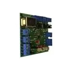
Figure 3. Top Assembly View
8
bq2403x (bqTiny-III™) 1.5-A Single-Chip Li-Ion
and Li-Pol Charge Management IC EVM
SLUU207A – October 2004 – Revised January 2007
Submit Documentation Feedback
�www.ti.com
Physical Layouts
Figure 4. Board Layout – Top Etch Layer
SLUU207A – October 2004 – Revised January 2007
Submit Documentation Feedback
bq2403x (bqTiny-III™) 1.5-A Single-Chip Li-Ion
and Li-Pol Charge Management IC EVM
9
�www.ti.com
Physical Layouts
Figure 5. Board Layout – Second Etch Layer
10
bq2403x (bqTiny-III™) 1.5-A Single-Chip Li-Ion
and Li-Pol Charge Management IC EVM
SLUU207A – October 2004 – Revised January 2007
Submit Documentation Feedback
�www.ti.com
Physical Layouts
Figure 6. Board Layout – Third Etch Layer
SLUU207A – October 2004 – Revised January 2007
Submit Documentation Feedback
bq2403x (bqTiny-III™) 1.5-A Single-Chip Li-Ion
and Li-Pol Charge Management IC EVM
11
�www.ti.com
Physical Layouts
Figure 7. Board Layout – Bottom Etch Layer
12
bq2403x (bqTiny-III™) 1.5-A Single-Chip Li-Ion
and Li-Pol Charge Management IC EVM
SLUU207A – October 2004 – Revised January 2007
Submit Documentation Feedback
�www.ti.com
Bill of Materials
7
Bill of Materials
Table 2. Bill of Materials (1) (2) (3) (4)
COUNT
bq24030
-001
bq24032
-002
bq24035
-003
bq24031
-004
REFDES
DESCRIPTION
SIZE
MFR
3
3
3
3
C1, C2, C3
2
2
2
2
C4, C5
1
1
1
1
0
0
0
0
0
1
1
3
1
PART NUMBER
Capacitor, ceramic, 10-µF, 6.3-V, X5R, 20%
805
Panasonic
ECJ-2FB0J106M
Capacitor, ceramic, 10-µF, 25-V, X5R, 20%
1206
Panasonic
ECJ-3YB1E106M
C6
Capacitor, ceramic, 0.47-µF, 16-V, X7R,
10%
805
Panasonic
ECJ-2YB1C474K
0
C7
Capacitor, ceramic, 0.22-µF, 10-V, X5R,
10%
603
Panasonic
ECJ-1VB1A224K
0
0
C8
Capacitor, ceramic, xxx-µF, 10-V, X5R, 10%
ECJ-1VB1C103K
1
1
D1
Diode, dual Schottky, 200-mA, 30-V
3
3
3
D2, D4, D5
1
1
1
D3
4
4
4
4
J1, J2, J5,
J7
1
1
1
1
3
3
3
3
1
1
1
7
7
4
603
Panasonic
SOT23
Vishay
-Liteon
BAT54C
Diode, LED, green, 2.1-V, 20-mA, 6-mcd
603
Liteon
160-1183-1-ND
Diode, LED, red, 1.8-V, 20-mA, 20-mcd
603
Liteon
160-1181-1-ND
Terminal block, 2-pin, 6-A, 3.5 mm
0.27 x 0.25
OST
ED1514
J3
Terminal block, 4-pin, 6-A, 3.5 mm
0.55 x 0.25
OST
ED1516
J4, J6, J8
Terminal block, 3-pin, 6-A, 3.5 mm
0.41 x 0.25
OST
ED1515
1
J9
Connector, USB upstream (Type B)
0.47 x 0.67
Molex
67068-1000
7
7
JMP1,
JMP2,
JMP3,
JMP4,
JMP5,
JMP6,
JMP7
Header, 3-pin, 100-mil spacing,
(36-pin strip)
0.10 x 3
Sullins
PTC36SAAN
4
4
4
R1, R2, R7,
R8
Resistor, Chip, 1.5-kΩ, 1/16-W, 1%
603
Std
Std
1
1
1
1
R10
Resistor, Chip, 0-Ω, 1/16-W, 1%
603
Std
Std
1
1
1
1
R11
Resistor, Chip, 22.6-kΩ, 1/16-W, 1%
603
Std
Std
1
1
1
1
R14
Resistor, Chip, 30.1-kΩ, 1/16-W, 1%
603
Std
Std
1
1
1
1
R15
Potentiometer, 20-kΩ, 1/4 inch Cermet,
12-turn, top-adjust
0.25 × 0.17
Bourns
3266W-203
1
1
1
1
R16
Potentiometer, 50-kΩ, 1/4 inch Cermet,
12-turn, top-adjust
0.25 × 0.17
Bourns
3266W-503
3
3
3
3
R3, R4, R5
Resistor, chip, 100-kΩ, 1/16-W, 1%
603
Std
Std
1
1
1
1
R6
Resistor, chip, 1-kΩ, 1/10W, 1%
805
Std
Std
1
1
1
1
R9
Resistor, chip, 10-kΩ, 1/16-W, 1%
603
Std
Std
3
3
3
3
TP1, TP2,
TP3
Test point, 0.032-inch hole
None
Void
1
U1
IC, single chip charge and power path
management
QFN
TI
bq24030RHL
U1
IC , single chip charge and power path
management
QFN
TI
bq24032ARHL
U1
IC , single chip charge and power path
management
QFN
TI
bq24035RHL
--
PCB, 2-inch x 2-inch x 0.31-inch
1
1
1
1
1
1
1
Any
HPA073
(1)
These assemblies are ESD sensitive, ESD precautions shall be observed.
(2)
These assemblies must be clean and free from flux and all contaminants. Use of no-clean flux is not acceptable.
(3)
These assemblies must comply with workmanship standards IPC-A-610 Class 2.
(4)
Reference designators marked with an asterisk ('**') cannot be substituted. All other components can be substituted with equivalent
MFR's components.
SLUU207A – October 2004 – Revised January 2007
Submit Documentation Feedback
bq2403x (bqTiny-III™) 1.5-A Single-Chip Li-Ion
and Li-Pol Charge Management IC EVM
13
�www.ti.com
References
8
References
1. SLUS618, bq2403x Datasheet
14
bq2403x (bqTiny-III™) 1.5-A Single-Chip Li-Ion
and Li-Pol Charge Management IC EVM
SLUU207A – October 2004 – Revised January 2007
Submit Documentation Feedback
�www.ti.com
References
FCC Warning
This evaluation board/kit is intended for use for ENGINEERING DEVELOPMENT,
DEMONSTRATION, OR EVALUATION PURPOSES ONLY and is not considered by TI to be a
finished end-product fit for general customer use. It generates, uses, and can radiate radio
frequency energy and has not been tested for compliance with the limits of computing devices
pursuant to part 15 of FCC rules, which are designed to provide reasonable protection against
radio frequency interference. Operation of this equipment in other environments may cause
interference with radio communications, in which case the user at his own expense will be
required to take whatever measures may be required to correct this interference.
EVALUATION BOARD/KIT IMPORTANT NOTICE
Texas Instruments (TI) provides the enclosed product(s) under the following conditions:
This evaluation board/kit is intended for use for ENGINEERING DEVELOPMENT,
DEMONSTRATION, OR EVALUATION PURPOSES ONLY and is not considered by TI to be a
finished end-product fit for general consumer use. Persons handling the product(s) must have
electronics training and observe good engineering practice standards. As such, the goods being
provided are not intended to be complete in terms of required design-, marketing-, and/or
manufacturing-related protective considerations, including product safety and environmental
measures typically found in end products that incorporate such semiconductor components or
circuit boards. This evaluation board/kit does not fall within the scope of the European Union
directives regarding electromagnetic compatibility, restricted substances (RoHS), recycling
(WEEE), FCC, CE or UL, and therefore may not meet the technical requirements of these
directives or other related directives.
Should this evaluation board/kit not meet the specifications indicated in the User’s Guide, the
board/kit may be returned within 30 days from the date of delivery for a full refund. THE
FOREGOING WARRANTY IS THE EXCLUSIVE WARRANTY MADE BY SELLER TO BUYER
AND IS IN LIEU OF ALL OTHER WARRANTIES, EXPRESSED, IMPLIED, OR STATUTORY,
INCLUDING ANY WARRANTY OF MERCHANTABILITY OR FITNESS FOR ANY PARTICULAR
PURPOSE.
The user assumes all responsibility and liability for proper and safe handling of the goods. Further,
the user indemnifies TI from all claims arising from the handling or use of the goods. Due to the
open construction of the product, it is the user’s responsibility to take any and all appropriate
precautions with regard to electrostatic discharge.
EXCEPT TO THE EXTENT OF THE INDEMNITY SET FORTH ABOVE, NEITHER PARTY
SHALL BE LIABLE TO THE OTHER FOR ANY INDIRECT, SPECIAL, INCIDENTAL, OR
CONSEQUENTIAL DAMAGES.
TI currently deals with a variety of customers for products, and therefore our arrangement with the
user is not exclusive.
TI assumes no liability for applications assistance, customer product design, software
performance, or infringement of patents or services described herein.
Please read the User’s Guide and, specifically, the Warnings and Restrictions notice in the User’s
Guide prior to handling the product. This notice contains important safety information about
temperatures and voltages. For additional information on TI’s environmental and/or safety
programs, please contact the TI application engineer or visit www.ti.com/esh.
No license is granted under any patent right or other intellectual property right of TI covering or
relating to any machine, process, or combination in which such TI products or services might be
or are used.
SLUU207A – October 2004 – Revised January 2007
Submit Documentation Feedback
bq2403x (bqTiny-III™) 1.5-A Single-Chip Li-Ion
and Li-Pol Charge Management IC EVM
15
�www.ti.com
References
FCC Warning
This evaluation board/kit is intended for use for ENGINEERING DEVELOPMENT,
DEMONSTRATION, OR EVALUATION PURPOSES ONLY and is not considered by TI to be a
finished end-product fit for general consumer use. It generates, uses, and can radiate radio
frequency energy and has not been tested for compliance with the limits of computing devices
pursuant to part 15 of FCC rules, which are designed to provide reasonable protection against
radio frequency interference. Operation of this equipment in other environments may cause
interference with radio communications, in which case the user at his own expense will be
required to take whatever measures may be required to correct this interference.
Mailing Address: Texas Instruments, Post Office Box 655303, Dallas, Texas 75265
Copyright © 2007, Texas Instruments Incorporated
EVM WARNINGS AND RESTRICTIONS
It is important to operate this EVM within the input voltage range of 0 V to 6.5 V and the output
voltage range of 0 V to 6.5 V.
Exceeding the specified input range may cause unexpected operation and/or irreversible damage
to the EVM. If there are questions concerning the input range, please contact a TI field
representative prior to connecting the input power.
Applying loads outside of the specified output range may result in unintended operation and/or
possible permanent damage to the EVM. Please consult the EVM User's Guide prior to
connecting any load to the EVM output. If there is uncertainty as to the load specification, please
contact a TI field representative.
During normal operation, some circuit components may have case temperatures greater than
85°C. The EVM is designed to operate properly with certain components above 60°C as long as
the input and output ranges are maintained. These components include but are not limited to
linear regulators, switching transistors, pass transistors, and current sense resistors. These types
of devices can be identified using the EVM schematic located in the EVM User's Guide. When
placing measurement probes near these devices during operation, please be aware that these
devices may be very warm to the touch.
Mailing Address: Texas Instruments, Post Office Box 655303, Dallas, Texas 75265
Copyright © 2007, Texas Instruments Incorporated
16
bq2403x (bqTiny-III™) 1.5-A Single-Chip Li-Ion
and Li-Pol Charge Management IC EVM
SLUU207A – October 2004 – Revised January 2007
Submit Documentation Feedback
�IMPORTANT NOTICE
Texas Instruments Incorporated and its subsidiaries (TI) reserve the right to make corrections, modifications, enhancements,
improvements, and other changes to its products and services at any time and to discontinue any product or service without notice.
Customers should obtain the latest relevant information before placing orders and should verify that such information is current and
complete. All products are sold subject to TI’s terms and conditions of sale supplied at the time of order acknowledgment.
TI warrants performance of its hardware products to the specifications applicable at the time of sale in accordance with TI’s
standard warranty. Testing and other quality control techniques are used to the extent TI deems necessary to support this
warranty. Except where mandated by government requirements, testing of all parameters of each product is not necessarily
performed.
TI assumes no liability for applications assistance or customer product design. Customers are responsible for their products and
applications using TI components. To minimize the risks associated with customer products and applications, customers should
provide adequate design and operating safeguards.
TI does not warrant or represent that any license, either express or implied, is granted under any TI patent right, copyright, mask
work right, or other TI intellectual property right relating to any combination, machine, or process in which TI products or services
are used. Information published by TI regarding third-party products or services does not constitute a license from TI to use such
products or services or a warranty or endorsement thereof. Use of such information may require a license from a third party under
the patents or other intellectual property of the third party, or a license from TI under the patents or other intellectual property of TI.
Reproduction of information in TI data books or data sheets is permissible only if reproduction is without alteration and is
accompanied by all associated warranties, conditions, limitations, and notices. Reproduction of this information with alteration is an
unfair and deceptive business practice. TI is not responsible or liable for such altered documentation.
Resale of TI products or services with statements different from or beyond the parameters stated by TI for that product or service
voids all express and any implied warranties for the associated TI product or service and is an unfair and deceptive business
practice. TI is not responsible or liable for any such statements.
TI products are not authorized for use in safety-critical applications (such as life support) where a failure of the TI product would
reasonably be expected to cause severe personal injury or death, unless officers of the parties have executed an agreement
specifically governing such use. Buyers represent that they have all necessary expertise in the safety and regulatory ramifications
of their applications, and acknowledge and agree that they are solely responsible for all legal, regulatory and safety-related
requirements concerning their products and any use of TI products in such safety-critical applications, notwithstanding any
applications-related information or support that may be provided by TI. Further, Buyers must fully indemnify TI and its
representatives against any damages arising out of the use of TI products in such safety-critical applications.
TI products are neither designed nor intended for use in military/aerospace applications or environments unless the TI products are
specifically designated by TI as military-grade or "enhanced plastic." Only products designated by TI as military-grade meet military
specifications. Buyers acknowledge and agree that any such use of TI products which TI has not designated as military-grade is
solely at the Buyer's risk, and that they are solely responsible for compliance with all legal and regulatory requirements in
connection with such use.
TI products are neither designed nor intended for use in automotive applications or environments unless the specific TI products
are designated by TI as compliant with ISO/TS 16949 requirements. Buyers acknowledge and agree that, if they use any
non-designated products in automotive applications, TI will not be responsible for any failure to meet such requirements.
Following are URLs where you can obtain information on other Texas Instruments products and application solutions:
Products
Applications
Amplifiers
amplifier.ti.com
Audio
www.ti.com/audio
Data Converters
dataconverter.ti.com
Automotive
www.ti.com/automotive
DSP
dsp.ti.com
Broadband
www.ti.com/broadband
Interface
interface.ti.com
Digital Control
www.ti.com/digitalcontrol
Logic
logic.ti.com
Military
www.ti.com/military
Power Mgmt
power.ti.com
Optical Networking
www.ti.com/opticalnetwork
Microcontrollers
microcontroller.ti.com
Security
www.ti.com/security
RFID
www.ti-rfid.com
Telephony
www.ti.com/telephony
Low Power
Wireless
www.ti.com/lpw
Video & Imaging
www.ti.com/video
Wireless
www.ti.com/wireless
Mailing Address: Texas Instruments, Post Office Box 655303, Dallas, Texas 75265
Copyright © 2007, Texas Instruments Incorporated
�