Order
Now
Product
Folder
Support &
Community
Tools &
Software
Technical
Documents
bq24080
bq24081
SLUS698F – MARCH 2006 – REVISED MAY 2017
BQ24080, BQ24081 1-A, Single-Chip, Li-Ion and Li-Pol Charger IC
1 Features
3 Description
•
The bq24080 and bq24081 are highly integrated and
flexible Li-Ion linear charge devices targeted at
space-limited charger applications. They offer an
integrated power FET and current sensor, highaccuracy current and voltage regulation, charge
status, and charge termination, in a single monolithic
device. An external resistor sets the magnitude of the
charge current.
1
•
•
•
•
•
•
•
Integrated Power FET and Current Sensor for Up
to 1-A Charge Applications From AC Adapter
Precharge Conditioning With Safety Timer
Charge and Power-Good Status Output
Automatic Sleep Mode for Low Power
Consumption
Integrated Charge-Current Monitor
Fixed 7-Hour Fast Charge Safety Timer
Ideal for Low-Dropout Charger Designs for SingleCell Li-Ion or Li-Pol Packs in Space-Limited
Portable Applications
Small 3.00-mm × 3.00-mm VSON Package
The device charges the battery in three phases:
conditioning, constant current, and constant voltage.
Charge is terminated based on minimum current. An
internal charge timer provides a backup safety for
charge termination. The device automatically restarts
the charge if the battery voltage falls below an
internal threshold. The device automatically enters
sleep mode when the ac adapter is removed.
2 Applications
•
•
•
•
PDAs, MP3 Players
Digital Cameras
Internet Appliances
Smartphones
Device Information(1)
PART NUMBER
bq24080
bq24081
PACKAGE
VSON (10)
BODY SIZE (NOM)
3.00 mm × 3.00 mm
(1) For all available packages, see the orderable addendum at
the end of the data sheet.
Typical Application
AC
Adapter
VDC
GND
C1
0.1 mF
PACK+
bq24080
1
IN
C2
0.1 µF
OUT 10
PACK–
2
GND
CE
9
3
STAT1
PG
8
4
STAT2
5
VSS
Battery Pack
+
System
System
Interface
GND 7
RSET
ISET
6
1.13 kW
Copyright © 2017, Texas Instruments Incorporated
1
An IMPORTANT NOTICE at the end of this data sheet addresses availability, warranty, changes, use in safety-critical applications,
intellectual property matters and other important disclaimers. PRODUCTION DATA.
�bq24080
bq24081
SLUS698F – MARCH 2006 – REVISED MAY 2017
www.ti.com
Table of Contents
1
2
3
4
5
6
7
Features ..................................................................
Applications ...........................................................
Description .............................................................
Revision History.....................................................
Pin Configuration and Functions .........................
Specifications.........................................................
1
1
1
2
3
4
6.1
6.2
6.3
6.4
6.5
6.6
4
4
4
4
5
7
Absolute Maximum Ratings ......................................
ESD Ratings..............................................................
Recommended Operating Conditions.......................
Thermal Information ..................................................
Electrical Characteristics...........................................
Typical Characteristics ..............................................
Detailed Description .............................................. 8
7.1 Overview ................................................................... 8
7.2 Functional Block Diagram ....................................... 10
7.3 Feature Description................................................. 11
7.4 Device Functional Modes........................................ 14
8
Application and Implementation ........................ 15
8.1 Application Information............................................ 15
8.2 Typical Application ................................................. 15
9 Power Supply Recommendations...................... 17
10 Layout................................................................... 18
10.1 Layout Guidelines ................................................. 18
11 Device and Documentation Support ................. 20
11.1
11.2
11.3
11.4
11.5
11.6
11.7
Documentation Support ........................................
Related Links ........................................................
Receiving Notification of Documentation Updates
Community Resources..........................................
Trademarks ...........................................................
Electrostatic Discharge Caution ............................
Glossary ................................................................
20
20
20
20
20
20
20
12 Mechanical, Packaging, and Orderable
Information ........................................................... 20
4 Revision History
NOTE: Page numbers for previous revisions may differ from page numbers in the current version.
Changes from Revision E (August 2011) to Revision F
Page
•
Added ESD Ratings table, Feature Description section, Device Functional Modes, Application and Implementation
section, Power Supply Recommendations section, Layout section, Device and Documentation Support section, and
Mechanical, Packaging, and Orderable Information section. ................................................................................................. 1
•
Changed pins 2 and 7 to GND in the Typical Application image .......................................................................................... 1
2
Submit Documentation Feedback
Copyright © 2006–2017, Texas Instruments Incorporated
Product Folder Links: bq24080 bq24081
�bq24080
bq24081
www.ti.com
SLUS698F – MARCH 2006 – REVISED MAY 2017
5 Pin Configuration and Functions
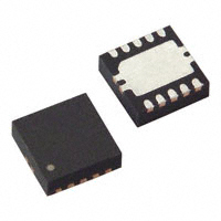
bq24080 DRC Package
10-Pin VSON
Top View
VSS STAT2 STAT1 GND
5
4
3
2
bq24081 DRC Package
10-Pin VSON
Top View
IN
VSS STAT2 STAT1 GND
1
5
4
Thermal
Pad
7
6
ISET GND
3
IN
2
1
8
9
10
TE
TS
Thermal
Pad
8
9
10
PG
CE OUT
6
7
ISET GND
OUT
Pin Functions
PIN
NAME
IN
NO.
bq24080
I/O
DESCRIPTION
bq24081
1
1
I
Adapter dc voltage. Connect minimum 0.1-μF capacitor to VSS.
2, 7
2, 7
–
Ground
STAT1
3
3
O
STAT2
4
4
O
VSS
5
5
–
Ground
ISET
6
6
I
Charge current. External resistor to VSS sets precharge and fast-charge current, and also the
termination current value. Can be used to monitor the charge current.
PG
8
–
O
Power-good status output (open-drain)
TE
–
8
I
Timer-enable input (active-low)
TS
–
9
I/O
CE
9
–
I
Charge enable input (active-low)
OUT
10
10
O
Charge current output. Connect minimum 0.1-μF capacitor to VSS.
Thermal
pad
–
–
–
There is an internal electrical connection between the exposed thermal pad and the VSS pin of the
device. The exposed thermal pad must be connected to the same potential as the VSS pin on the
printed-circuit board. Do not use the thermal pad as the primary ground input for the device.
The VSS pin must be connected to ground at all times.
GND
Charge status outputs (open-drain)
Temperature sense; connect to NTC in battery pack.
Submit Documentation Feedback
Copyright © 2006–2017, Texas Instruments Incorporated
Product Folder Links: bq24080 bq24081
3
�bq24080
bq24081
SLUS698F – MARCH 2006 – REVISED MAY 2017
www.ti.com
6 Specifications
6.1 Absolute Maximum Ratings
over operating free-air temperature range (unless otherwise noted) (1)
VI
MIN
MAX
UNIT
–0.3
7
V
STAT1, STAT2, PG
15
mA
OUT
1.5
Input voltage (2)
IN, CE, ISET, OUT, PG, STAT1, STAT2, TE, TS
Output sink/source current
Output current
TA
Operating free-air temperature range
TJ
Junction temperature range
Tstg
Storage temperature
(1)
(2)
–40
125
–65
150
A
°C
°C
°C
Stresses beyond those listed under Absolute Maximum Ratings may cause permanent damage to the device. These are stress ratings
only, which do not imply functional operation of the device at these or any other conditions beyond those indicated under Recommended
Operating Conditions. Exposure to absolute-maximum-rated conditions for extended periods may affect device reliability.
All voltages are with respect to VSS.
6.2 ESD Ratings
VALUE
V(ESD)
(1)
(2)
Electrostatic discharge
Human-body model (HBM), per ANSI/ESDA/JEDEC JS-001 (1)
±2000
Charged-device model (CDM), per JEDEC specification JESD22C101 (2)
±500
UNIT
V
JEDEC document JEP155 states that 500-V HBM allows safe manufacturing with a standard ESD control process.
JEDEC document JEP157 states that 250-V CDM allows safe manufacturing with a standard ESD control process.
6.3 Recommended Operating Conditions
over operating free-air temperature range (unless otherwise noted)
VCC
Supply voltage
TJ
Operating junction temperature range
MIN
MAX
4.5
6.5
UNIT
V
0
125
°C
6.4 Thermal Information
bq2408x
THERMAL METRIC
(1)
DRC (VSON)
UNIT
10 PINS
RθJA
Junction-to-ambient thermal resistance
49.4
°C/W
RθJC(top)
Junction-to-case (top) thermal resistance
69.8
°C/W
RθJB
Junction-to-board thermal resistance
23.9
°C/W
ψJT
Junction-to-top characterization parameter
2.1
°C/W
ψJB
Junction-to-board characterization parameter
24.1
°C/W
RθJC(bot)
Junction-to-case (bottom) thermal resistance
6.1
°C/W
(1)
4
For more information about traditional and new thermal metrics, see the Semiconductor and IC Package Thermal Metrics application
report.
Submit Documentation Feedback
Copyright © 2006–2017, Texas Instruments Incorporated
Product Folder Links: bq24080 bq24081
�bq24080
bq24081
www.ti.com
SLUS698F – MARCH 2006 – REVISED MAY 2017
6.5 Electrical Characteristics
over 0°C ≤ TJ ≤ 125°C and recommended supply voltage (unless otherwise noted)
PARAMETER
TEST CONDITIONS
MIN
TYP
MAX
1.2
2
2
5
UNIT
INPUT CURRENT
ICC(VCC)
VCC current
VCC > VCC(min)
ICC(SLP)
Sleep current
Sum of currents into OUT pin,
VCC < V(SLP)
ICC(STBY)
Standby current
CE = High, 0°C ≤ TJ ≤ 85°C
IIB(OUT)
Input current on OUT pin
Charge DONE, VCC > VCC(MIN)
150
1
mA
μA
5
VOLTAGE REGULATION VO(REG) + V(DO−MAX) ≤ VCC, I(TERM) < IO(OUT) ≤ 1 A
VO(REG)
Output voltage
Voltage regulation accuracy
V(DO)
Dropout voltage (V(IN) − V(OUT))
4.2
TA = 25°C
V
−0.35%
0.35%
−1%
1%
VO(OUT) = VO(REG), IO(OUT) = 1 A
VO(REG) + V(DO)) ≤ VCC
350
500
mV
1000
mA
V
CURRENT REGULATION
IO(OUT)
Output current range (1)
VI(OUT) > V(LOWV),
VI(IN) − VI(OUT) > V(DO),
VCC ≥ 4.5 V
V(SET)
Output current set voltage
Voltage on ISET pin, VCC ≥ 4.5 V,
VI ≥ 4.5 V, VI(OUT) > V(LOWV),
VI − VI(OUT) > V(DO)
K(SET)
Output current set factor
20
2.463
2.5
2.538
50 mA ≤ IO(OUT) ≤ 1 A
307
322
337
10 mA ≤ IO(OUT) < 50 mA
296
320
346
1 mA ≤ IO(OUT) < 10 mA
246
320
416
PRECHARGE AND SHORT-CIRCUIT CURRENT REGULATION
Precharge to fast-charge transition
threshold
Voltage on OUT pin
2.8
3
3.2
V
Deglitch time for fast-charge to
precharge transition
VCC(MIN) ≥ 4.5 V, tFALL = 100 ns,
10-mV overdrive,
VI(OUT) decreasing below threshold
250
375
500
ms
IO(PRECHG)
Precharge range (2)
0 V < VI(OUT) < V(LOWV), t < t(PRECHG)
2
100
mA
V(PRECHG)
Precharge set voltage
Voltage on ISET pin,
VO(REG) = 4.2 V,
0 V < VI(OUT) > V(LOWV), t < t(PRECHG)
240
270
mV
100
mA
V(LOWV)
255
TERMINATION DETECTION
I(TERM)
Charge termination detection
range (3)
VI(OUT) > V(RCH), t < t(TRMDET)
2
V(TERM)
Charge termination detection set
voltage
Voltage on ISET pin,
VO(REG) = 4.2 V,
VI(OUT) > V(RCH), t < t(TRMDET)
235
250
265
mV
tTRMDET
Deglitch time for termination
detection
VCC(MIN) ≥ 4.5 V, tFALL = 100 ns
charging current decreasing below
10-mV overdrive
250
375
500
ms
(1)
(2)
(3)
See Equation 2 in the Function Description section.
See Equation 1 in the Function Description section.
See Equation 4 in the Function Description section.
Submit Documentation Feedback
Copyright © 2006–2017, Texas Instruments Incorporated
Product Folder Links: bq24080 bq24081
5
�bq24080
bq24081
SLUS698F – MARCH 2006 – REVISED MAY 2017
www.ti.com
Electrical Characteristics (continued)
over 0°C ≤ TJ ≤ 125°C and recommended supply voltage (unless otherwise noted)
PARAMETER
TEST CONDITIONS
MIN
TYP
MAX
UNIT
VO(REG)
– 0.115
VO(REG)
− 0.10
VO(REG)
− 0.085
250
375
500
ms
0.25
V
BATTERY RECHARGE THRESHOLD
V(RCH)
Recharge threshold
t(DEGL)
Deglitch time for recharge detect
VCC(MIN) ≥ 4.5 V, tFALL = 100 ns
decreasing below or increasing
above threshold, 10-mV overdrive
V
STAT1, STAT2, and PG OUTPUTS
VOL
Low-level output saturation voltage
IO = 5 mA
CE and TE INPUTS
VIL
Low-level input voltage
0
VIH
High-level input voltage
1.4
IIL
Low-level input current
–1
IIH
High-level input current
0.4
1
V
μA
TIMERS
t(PRECHG)
Precharge time
t(CHG)
Charge time
I(FAULT)
Timer fault recovery current
1,584
1,800
2,016
22,176
25,200
28,224
200
s
s
μA
SLEEP COMPARATOR
V(SLP)
Sleep-mode entry threshold voltage
V(SLPEXIT)
Sleep-mode exit threshold voltage
2.3 V ≤ VI(OUT) ≤ VO(REG)
Sleep-mode entry deglitch time
V(IN) decreasing below threshold,
tFALL = 100 ns, 10-mV overdrive
VCC ≤ VI(OUT)
+ 80 mV
VCC ≥ VI(OUT)
+ 190
250
375
500
V
ms
THERMAL SHUTDOWN THRESHOLDS
T(SHTDWN)
Thermal trip threshold
Thermal hysteresis
165
TJ increasing
°C
15
UNDERVOLTAGE LOCKOUT
UVLO
Undervoltage lockout
Decreasing VCC
2.4
Hysteresis
2.5
2.6
27
V
mV
TEMPERATURE SENSE COMPARATOR (bq24081)
V(TS1)
High-voltage threshold
2.475
2.5
2.525
V(TS2)
Low-voltage threshold
0.485
0.5
0.515
I(TS)
TS pin current source
96
102
108
μA
t(DEGL)
Deglitch time for temperature fault
250
375
500
ms
6
Submit Documentation Feedback
V
Copyright © 2006–2017, Texas Instruments Incorporated
Product Folder Links: bq24080 bq24081
�bq24080
bq24081
www.ti.com
SLUS698F – MARCH 2006 – REVISED MAY 2017
6.6 Typical Characteristics
450
IO(OUT) = 1000 mA
400
Dropout Voltage - mV
350
IO(OUT) = 750 mA
300
250
IO(OUT) = 500 mA
200
150
IO(OUT) = 250 mA
100
50
0
0
50
100
o
TJ - Junction Temperature - C
150
Figure 1. Dropout Voltage vs Junction Temperature
Figure 2. VIN Hot-Plug Power-Up Sequence
Figure 3. Charge Enable Power-Up Sequence
(CE = High-to-Low)
Figure 4. Battery Hot-Plug During Charging Phase
No battery – In termination deglitch prior to STAT1 going high. VOUT (VBAT) cycling between charge and done prior to screen capture
Stat1 goes high – In done state
2-V battery is inserted during the charge done state.
Charging is initiated – STAT1 goes low and charge current is applied.
Battery is removed – VOUT goes into regulation, IOUT goes to zero, and termination deglitch timer starts running (same as state 1).
Deglitch timer expires – charge done is declared.
Figure 5. Battery Hot-Plug and Removal Power Sequence
Submit Documentation Feedback
Copyright © 2006–2017, Texas Instruments Incorporated
Product Folder Links: bq24080 bq24081
7
�bq24080
bq24081
SLUS698F – MARCH 2006 – REVISED MAY 2017
www.ti.com
7 Detailed Description
7.1 Overview
The device supports a precision Li-Ion, Li-Pol charging system suitable for single cells. Figure 6 shows a typical
charge profile, and Figure 7 shows an operational flow chart.
Preconditioning
Phase
Current Regulation Phase
Voltage Regulation and Charge Termination Phase
Regulation
Voltage
Regulation
Current
Minimum
Charge
Voltage
PreConditioning
and Term
Detect
Charge
Voltage
Charge
Complete
Charge
Current
Safety Timer
M0066-01
Figure 6. Typical Charging Profile
8
Submit Documentation Feedback
Copyright © 2006–2017, Texas Instruments Incorporated
Product Folder Links: bq24080 bq24081
�bq24080
bq24081
www.ti.com
SLUS698F – MARCH 2006 – REVISED MAY 2017
Overview (continued)
POR
SLEEP MODE
VCC > VI(OUT)
checked at all
times?
No
Indicate SLEEP
MODE
Yes
VI(OUT)


 工商网监
湘ICP备2023018690号
工商网监
湘ICP备2023018690号
