User's Guide
SLUU507A – June 2011 – Revised September 2011
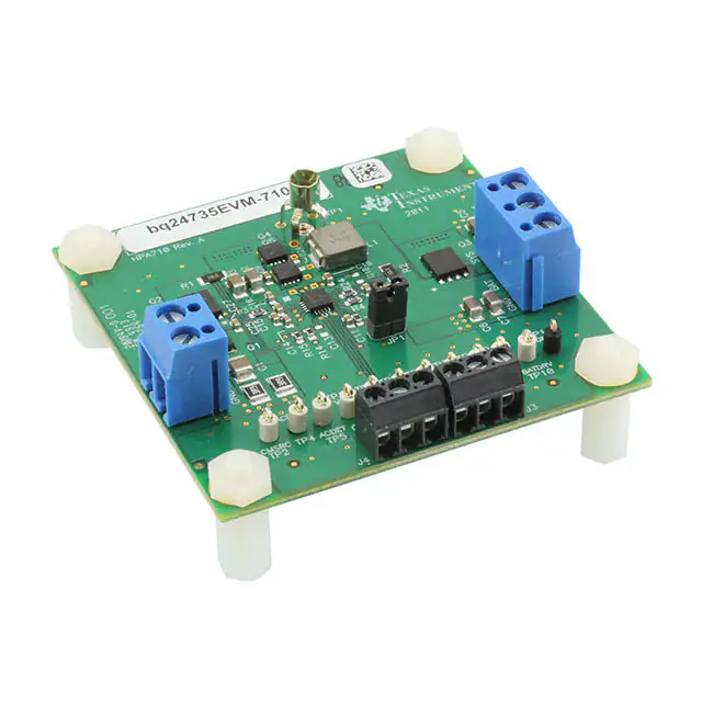
bq24735/725A Battery Charger Evaluation Module
This user's guide describes the features and operation of the bq24725A/735EVM Evaluation Module.
1
2
3
4
Contents
Introduction .................................................................................................................. 2
1.1
EVM Features ...................................................................................................... 2
1.2
General Description ................................................................................................ 2
1.3
Input/Output Jack Description .................................................................................... 2
1.4
Control and Key Parameters Setting ............................................................................ 3
1.5
Recommended Operating Conditions ........................................................................... 3
Test Summary ............................................................................................................... 3
2.1
Definitions ........................................................................................................... 3
2.2
Equipment ........................................................................................................... 3
2.3
Equipment Setup ................................................................................................... 4
2.4
Procedure ........................................................................................................... 6
Printed-Circuit-Board Layout Guideline .................................................................................. 8
Bill of Materials, Board Layout, and Schematics ...................................................................... 10
4.1
Board Layouts ..................................................................................................... 12
4.2
Schematics ........................................................................................................ 18
List of Figures
1
EV2300 Kit Connections ................................................................................................... 5
2
Original Test Setup for HPA710
3
Main Window of bq24725A/735 Evaluation Software .................................................................. 6
4
Test Setup for HPA710..................................................................................................... 7
5
Top Assembly .............................................................................................................. 12
6
Top Layer ................................................................................................................... 13
7
Second Layer .............................................................................................................. 14
8
Third Layer ................................................................................................................. 15
9
Bottom Layer ............................................................................................................... 16
10
Bottom Assembly .......................................................................................................... 17
11
Schematic
..........................................................................................
..................................................................................................................
5
18
List of Tables
1
EV2300 and bq24725A/735EVM Connections.......................................................................... 5
2
Bill of Materials............................................................................................................. 10
Intel is a trademark of Intel Corporation.
Windows is a trademark of Microsoft Corporation.
SLUU507A – June 2011 – Revised September 2011
Submit Documentation Feedback
bq24735/725A Battery Charger Evaluation Module
Copyright © 2011, Texas Instruments Incorporated
1
�Introduction
1
Introduction
1.1
EVM Features
•
•
•
•
•
•
•
•
•
•
1.2
www.ti.com
Evaluation module for bq24725A/735
bq24735 adapter and battery together provide power to system to support Intel™ CPU Turbo Boost
mode
High-efficiency NMOS-NMOS synchronous buck charger with 750-kHz frequency
High-efficiency and low-cost NMOS power path selector and integrated gate driver
User-selectable 1-cell, 2-cell, 3-cell, or 4-cell Li-ion battery voltage
Programmable battery voltage, charge current, and ac adapter current via SMBus interface
Flexible Chargeoption() register control via SMBus interface
AC adapter operating range 4.5 V–24 V
Test points for key signals available for testing purposes. Easy probe hook-up
Jumpers available. Easy-to-change connections
General Description
The bq24725A/735 evaluation module (EVM) is a complete charger module for evaluating a multicell
synchronous notebook turbo boost charge using the bq24725A/735 devices. It is designed to deliver up to
4 A of charge current to Li-ion or Li-polymer applications. The charge current is programmable by SMBus
interface through the EV2300 interface board.
The bq24725A/735EVM does not include the EV2300 interface board. In order to evaluate the
bq24725A/735EVM, a user must order the EV2300 interface board separately.
The bq24725A/735 is a high-efficiency, synchronous battery charger, offering low component count for
space-constraint, multichemistry battery charging applications.
The bq24735 supports the Turbo Boost mode by allowing the battery to discharge energy to the system
when system power demand is temporarily higher than adapter maximum power level so that the adapter
does not crash.
The bq24725A/735 uses two charge pumps to separately drive n-channel MOSFETs (ACFET, RBFET,
and BATFET) for automatic system power source selection.
SMBus-controlled input current, charge current, and charge voltage DACs allow for high regulation
accuracies that can be easily programmed by the system power management microcontroller.
To throttle down PWM modulation and reduce the charge current, the bq24725A/735 uses the internal
input current register or the external ILIM pin .
The bq24725A/735 charges one, two, three, or four series Li+ cells and is available in a 20-pin, 3.5 x 3.5
mm2 QFN package. For details, see the bq24725A/735 data sheet (SLUSAK9).
1.3
2
Input/Output Jack Description
Jack
Description
J1–DCIN
AC adapter, positive output
J1–GND
AC adapter, negative output
J2-SYS
Connected to system
J2-BAT
Connected to battery pack
J2-GND
Ground
J3-ACOK
ACOK pin
J3-IOUT
IOUT pin
J3-3.3V
External voltage supply, 3.3 V
J4–SCL
SCL pin output, SMBus clock line
J4–SDA
SDA pin output, SMBus data line
bq24735/725A Battery Charger Evaluation Module
SLUU507A – June 2011 – Revised September 2011
Submit Documentation Feedback
Copyright © 2011, Texas Instruments Incorporated
�Test Summary
www.ti.com
1.4
1.5
Jack
Description
J4– GND
External power supply, negative output
Control and Key Parameters Setting
Jack
Description
Factory Setting
JMP1
Connect battery voltage to VCC pin
Jumper installed
Recommended Operating Conditions
Min
Typ
Max
Unit
Supply voltage, VIN
Input voltage from ac adapter input
18
19-20
22
V
Battery voltage, VBAT
Voltage applied at VBAT terminal
0
3-16.8
20
V
Supply current, IAC
Maximum input current from ac adapter
input
0
4.5
A
Charge current, Ichrg
Battery charge current
1
Operating junction temperature range, TJ
2
Test Summary
2.1
Definitions
0
3
4
A
125
°C
Notes
This procedure details how to configure the HPA710 evaluation board. On the test procedure, the
following naming conventions are followed. See the HPA710 schematic for details.
VXXX
LOADW
V(TPyyy)
V(Jxx)
V(TP(XXX))
External voltage supply name (VADP, VBT, VSBT)
External load name (LOADR, LOADI)
Voltage at internal test point TPyyy. For example, V(TP12) means the voltage at TP12.
Voltage at jack terminal Jxx
Voltage at test point XXX. For example, V(ACDET) means the voltage at the test point
which is marked as ACDET.
V(XXX, YYY)
Voltage across point XXX and YYY.
I(JXX(YYY))
Current going out from the YYY terminal of jack XX.
Jxx(BBB)
Terminal or pin BBB of jack xx
Jxx ON
Internal jumper Jxx terminals are shorted.
Jxx OFF
Internal jumper Jxx terminals are open.
Jxx (-YY-) ON
Internal jumper Jxx adjacent terminals marked as YY are shorted.
Measure: → A,B Check specified parameters A, B. If measured values are not within specified limits,
the unit under test has failed.
Observe → A,B Observe if A,B occur. If they do not occur, the unit under test has failed.
Assembly drawings have location for jumpers, test points, and individual components.
2.2
Equipment
Power Supplies
Power Supply #1 (PS#1): a power supply capable of supplying 20 V at 5 A is required.
Power Supply #2 (PS#2): a power supply capable of supplying 5 V at 1 A is required.
Power Supply #3 (PS#3): a power supply capable of supplying 20 V at 5 A is required.
SLUU507A – June 2011 – Revised September 2011
Submit Documentation Feedback
bq24735/725A Battery Charger Evaluation Module
Copyright © 2011, Texas Instruments Incorporated
3
�Test Summary
www.ti.com
Load #1
A 30-V (or above), 5-A (or above) electronic load that can operate at constant current mode
Load #2
A HP 6060B 3-V to 60-V/0-A to 60-A, 300-W system dc electronic load or equivalent
Meters
Seven Fluke 75 multimeters, (equivalent or better)
Or four equivalent voltage meters and three equivalent current meters.
The current meters must be capable of measuring 5-A+ current.
Computer
A computer with at least one USB port and a USB cable. The EV2300 USB driver and the
bq24725A/735 SMB evaluation software must be properly installed.
EV2300 SMBus Communication Kit
An EV2300 SMBUS communication kit
Software
Install the EV2300 driver before installing the bq24725A/735 software.
Driver (USB EV2300) Installer XP2K – Last updated Jan28-04.zip or later: This is the EV2300 USB
driver. Save and unzip to c:\temp (or other local directory). Double-click on the setup.exe file. Perform the
following installation steps.
1. This software needs to be installed after the EV2300 USB driver.
• bq2473x EVSW setup.zip (SLUC258): This is the bq24725A/735 SMB evaluation software. Save
and unzip to c:\temp (or other local directory). Double-click on the setup.exe file. Perform the
following steps.
• Note that on first insertion of EV2300 into the USB port of personal computer (PC), the user needs
to follow the instructions of the Found New Hardware wizard.
• Allow the Windows™ operating system to connect to Windows Update to search for software.
Then click Next.
• Select Install software automatically (Recommended). Then click Next.
• If a window pops up informing that the TI USB Firmware Updater has not passed Windows Logo
testing, click Continue Anyway.
• If a target file already exists and is newer, do not overwrite the newer file.
• Click Finish.
2.3
Equipment Setup
1. Set the power supply #1 for 0 V ± 100 mVdc, with the current limit set to > 5 A, and then turn off
supply.
2. Connect the output of power supply #1 in series with a current meter (multimeter) to J1 (DCIN, GND).
3. Connect a voltage meter across J1 (DCIN, GND).
4. Set the power supply #2 for 3.3 V ± 100 mVdc, 0.2-A ± 0.1-A current limit, and then turn off supply.
5. Connect the output of the power supply #2 to J3 (3.3 V) and J4 (GND).
6. Connect a voltage meter across J2 (BAT, GND).
7. Connect a voltage meter across J2 (SYS, GND).
8. Connect J4 (SDA, SCL) and J4 (GND) to the EV2300 kit SMB port. See Table 1 for a connection
reference. Connect the USB port of the EV2300 kit to the USB port of the computer. The connections
are shown in Figure 1.
4
bq24735/725A Battery Charger Evaluation Module
SLUU507A – June 2011 – Revised September 2011
Submit Documentation Feedback
Copyright © 2011, Texas Instruments Incorporated
�Test Summary
www.ti.com
Table 1. EV2300 and bq24725A/735EVM Connections
SCL (J4)
SMBC (2)
SDA (J4)
SMBD (3)
USB
EV2300
HDQ
GND (1)
VCC
HDQ
VOUT
GND
I2C
EV2300
GND (J4)
VOUT
SDA
SCL
GND
SMB
bq24725A/735EVM-710
NC
SMBD
SMBC
GND
HPA002
To Computer
USB port
2003
SDA
SCL
GND
To EVM
Figure 1. EV2300 Kit Connections
9. If JP1 is not installed, install the jumper.
10. After performing the preceding steps, the test setup for HPA710 is configures as is shown in Figure 2.
HPA710
TP1
bq247xxEVM
Power
supply #1
I in
SYS
J1
I
BAT
DCIN
V
V
J2
U1
V
GND
GND
GND
SDA
SCL
3.3V
IOUT
ACOK
APPLICATION CIRCUIT
J4
J3
EV2300
USB
Power
supply #2
Figure 2. Original Test Setup for HPA710
11. Turn on the computer. Open the bq24725A/735 evaluation software. The main window of the software
appears as is shown in Figure 3.
SLUU507A – June 2011 – Revised September 2011
Submit Documentation Feedback
bq24735/725A Battery Charger Evaluation Module
Copyright © 2011, Texas Instruments Incorporated
5
�Test Summary
www.ti.com
Figure 3. Main Window of bq24725A/735 Evaluation Software
2.4
2.4.1
Procedure
AC Adapter Detection Threshold
1. Ensure that Section 2.3 steps are followed. Turn on PS#2.
Note: Load #1 and Load #2 are not connected during this step.
2. Turn on PS#1.
3. Increase the output voltage of PS#1 to 19.5 V.
Measure → V(TP(ACDET)) = 2.6 V ± 0.1 V
Measure → V(TP(ACOK)) = 3.3 V ± 0.1 V
Measure → V(J2(SYS)) = 19.5 V ± 0.5 V
Measure → V(TP(REGN)) = 6 V ± 0.5 V
Measure → V(TP(ACDRV, CMSRC)) = 6 V ± 0.5 V
Measure → V(J2(BAT, GND)) = 2 V ± 2 V
2.4.2
Charger Parameters Setting
1. In the software main window, click all the Read buttons. Ensure that no error information is
generated.
2. If the error information window pops up and you see USB Error. Insure USB cable is connected
and Driver is working., do the following steps.
a) Click OK. Then, close main window, as shown in Figure 3, and disconnect USB cable.
b) Check 3.3-V power supply (PS#2) and power supply #1 (PS#1) voltage on the EVM board.
6
bq24735/725A Battery Charger Evaluation Module
SLUU507A – June 2011 – Revised September 2011
Submit Documentation Feedback
Copyright © 2011, Texas Instruments Incorporated
�Test Summary
www.ti.com
c) Disconnect any other unsure SMBus connection. Plug USB cable back to the original
EVM2300 installation USB port.
d) Open the bq24725A/735 evaluation software. The main window of the software is shown in
Figure 3.
3. In the software main window, click all the Read buttons.
a) Type in 512 (mA) in the Charge Current DAC, and click Write. This sets the battery charge
current regulation threshold.
b) Type in 12592 (mV) in the Charge Voltage DAC, and click Write. This sets the battery voltage
regulation threshold.
c) Measure → V(J2(BAT)) = 12.6 V ± 200 mV
2.4.3
Charge Current and ac Current Regulation, DPM
1. Type in 7801 in the Charge Option, and click Write; this disable
charging.
2. Connect the Load #2 in series with a current meter (multimeter) to J2 (BAT, GND).
Ensure that a voltage meter is connected across J2 (BAT, GND). Turn on the Load #2. Use the
constant voltage mode. Set the output voltage to 10.5 V.
3. Connect the output of the Load #1 in series with a current meter (multimeter) to J2 (SYS, GND).
Ensure that a voltage meter is connected across J2 (SYS, GND). Turn on the power of the Load
#1. Set the load current to 3 A ± 50 mA but disable the output. The setup is now like Figure 4 for
HPA710. Ensure that Ibat = 0 A ± 10 mA and Isys = 0 A ± 10 mA.
HPA710
bq247xxEVM
TP1
V
J2
U1
Isys
I
Load
#1
I
Load
#2
SYS
Power
supply #1
I in
J1
I
V
BAT
DCIN
GND
V
GND
Ibat
J4
3.3V
IOUT
ACOK
GND
SDA
SCL
APPLICATION CIRCUIT
J3
EV2300
USB
Power
supply #2
Figure 4. Test Setup for HPA710
4. Type in 7800 in the Charge Option, and click Write, this enable charging.
Measure → Ibat = 500 mA ± 100 mA
SLUU507A – June 2011 – Revised September 2011
Submit Documentation Feedback
bq24735/725A Battery Charger Evaluation Module
Copyright © 2011, Texas Instruments Incorporated
7
�Printed-Circuit-Board Layout Guideline
www.ti.com
5. Type in 2944 (mA) in the Charge Current DAC and click Write. This sets the battery charge current
regulation threshold to 2.944A.
Measure → Ibat = 3000 mA ± 300 mA
Measure → V(TP(IOUT)) = 340 mV ± 40 mV
6. Enable the output of the Load #1.
Measure → Isys = 3000 mA ± 300 mA, Ibat = 1600 mA ± 300 mA, Iin = 4100 mA ± 400 mA
Measure → V(TP(IOUT)) = 820 mV ± 100 mV
7. Turn off the Load #1.
Measure → Isys = 0 ± 100 mA, Ibat = 3000 mA ± 300 mA.
2.4.4
Boost Mode – bq24735EVM Only
1.
2.
3.
4.
Set ChargeOption() bit [3] to 1, and click Write; this enables turbo boost function.
Replace Load #2 with PS#3. Ensure that a voltage meter is connected across J2 (BAT, GND).
Enable the output of the PS #3. Ensure that the output voltage is 10 V ± 500 mV.
Set the Load#1 load current to 5 A ± 50 mA. Enter boost mode
Measure → ISYS = 5000 mA ± 500 mA, IBAT = -2000 mA ± 300 mA, IIN = 4100 mA ± 400 mA
5. Set the Load#1 load current to 3 A ± 50 mA. Exit boost mode.
Measure → ISYS = 3000 mA ± 500 mA, IBAT = 1600 mA ± 300 mA, IIN = 4100 mA ± 400 mA
2.4.5
Power Path Selection
1. Type in 7801 in the Charge Option, and click Write; this disable charging.
Measure → V(J2(SYS)) = 19.5 V ± 1 V (adapter connected to system)
2. Turn off PS#1. (PS#3 setting per Section 2.4.4, Step 2 and Step 3.
Measure → V(J2(SYS)) = 10 V ± 1 V (battery connected to system)
Measure → V(J2(BAT)) = 10 V ± 1 V (battery connected to system)
3
Printed-Circuit-Board Layout Guideline
The switching node rise and fall times must be minimized for minimum switching loss. Proper layout of the
components to minimize high-frequency, current-path loop is important to prevent electrical and magnetic
field radiation and high-frequency resonant problems. The following is a printed-circuit-board (PCB) layout
priority list for proper layout. Layout of the PCB according to this specific order is essential.
1. Place input capacitor as close as possible to switching MOSFET’s supply and ground connections, and
use the shortest copper trace connection. These parts must be placed on the same layer of the PCB
instead of on different layers and using vias to make this connection.
2. The integrated circuit (IC) must be placed close to the switching MOSFET’s gate terminals and the
gate drive signal traces kept short for a clean MOSFET drive. The IC can be placed on the other side
of the PCB of switching MOSFETs.
3. Place the inductor input terminal as close as possible to the switching MOSFET’s output terminal .
Minimize the copper area of this trace in order to lower electrical and magnetic field radiation, but make
the trace wide enough to carry the charging current. Do not use multiple layers in parallel for this
connection. Minimize parasitic capacitance from this area to any other trace or plane.
4. The charging current-sensing resistor must be placed right next to the inductor output. Route the sense
leads connected across the sensing resistor back to the IC in the same layer, close to each other
(minimize loop area), and do not route the sense leads through a high-current path. Place decoupling
capacitor on these traces next to the IC.
5. Place output capacitor next to the sensing resistor output and ground.
8
bq24735/725A Battery Charger Evaluation Module
SLUU507A – June 2011 – Revised September 2011
Submit Documentation Feedback
Copyright © 2011, Texas Instruments Incorporated
�Printed-Circuit-Board Layout Guideline
www.ti.com
6. The output capacitor ground connections need to be tied to the same copper that connects to the
input capacitor ground before connecting to the system ground.
7. Use single ground connection to tie the charger power ground to the charger analog ground. Just
beneath the IC, use analog ground copper pour, but avoid the power pins in order to reduce inductive
and capacitive noise coupling.
8. Route the analog ground separately from the power ground. Connect the analog ground, and then
connect the power ground separately. Connect analog ground and power ground together using power
pad as the single ground connection point. Or use a 0-Ω resistor to tie analog ground to the power
ground. (The power pad must tie to the analog ground in this case, if possible).
9. Place the decoupling capacitors next to the IC pins, and make the trace connection as short as
possible.
10. It is critical that the exposed power pad on the backside of the IC package be soldered to the PCB
ground. Ensure that sufficient thermal vias are located directly under the IC, connecting to the ground
plane on the other layers.
SLUU507A – June 2011 – Revised September 2011
Submit Documentation Feedback
bq24735/725A Battery Charger Evaluation Module
Copyright © 2011, Texas Instruments Incorporated
9
�Bill of Materials, Board Layout, and Schematics
4
www.ti.com
Bill of Materials, Board Layout, and Schematics
Table 2. Bill of Materials
-001
bq24725A
-002
bq24735
1
6
10
RefDes
Value
Description
Size
Part Number
MFR
1
C1
2.2 µF
Capacitor, Ceramic, 25V, X7R, 10%
1210
Std
Std
6
C2, C3, C4, C5, C6, C7
10 µF
Capacitor, Ceramic, 25V, X7R, 10%
1206
Std
Std
6
6
C8, C14, C15, C16, C17,
C19
0.1 µF
Capacitor, Ceramic, 25V, X7R, 10%
603
Std
Std
4
4
C9, C10, C20, C25
1 µF
Capacitor, Ceramic, 25V, X7R, 10%
603
Std
Std
3
3
C11, C12, C27
0.01 µF
Capacitor, Ceramic, 25V, X7R, 10%
603
Std
Std
0
0
C13, C18, C24
Open
Capacitor, Ceramic, 25V, X7R, 10%
603
Std
Std
1
1
C21
0.047 µF
Capacitor, Ceramic, 25V, X7R, 10%
603
Std
Std
1
1
C22
100 pF
Capacitor, Ceramic, 25V, X7R, 10%
603
Std
Std
1
1
C23
2200 pF
Capacitor, Ceramic, 25V, X7R, 10%
603
Std
Std
1
1
C26
1000 pF
Capacitor, Ceramic, 25V, X7R, 10%
603
Std
Std
1
1
D1
BAT54-V-G
Diode, Schottky, 200-mA, 30-V
SOT23
BAT54-V-G
Vishay-Liteon
1
1
D2
BAT54C-V-G
Diode, Dual Schottky, 200-mA, 30-V
SOT23
BAT54C-V-G
Vishay-Liteon
1
1
J1
ED120/2DS
Terminal Block, 2-pin, 15-A, 5.1mm
0.40 x 0.35 inch
ED120/2DS
OST
1
1
J2
ED120/3DS
Terminal Block, 3-pin, 15-A, 5.1mm
0.60 x 0.35 inch
ED120/3DS
OST
2
2
J3. J4
ED555/3DS
Terminal Block, 3-pin, 6-A, 3.5mm
0.41 x 0.25 inch
ED555/3DS
OST
1
1
JP1
PEC02SAAN
Header, Male 2-pin, 100mil spacing,
0.100 inch x 2
PEC02SAAN
Sullins
1
1
SH1
929950-00
Shorting jumpers, 2-pin, 100mil spacing,
929950-00
3M/ESD
1
1
L1
4.7 µH
Inductor, SMT
0.255 x 0.270 inch
IHLP2525CZER4R7M01
Vishay
3
3
Q1, Q2, Q3
CSD17307Q5A
MOSFET, NChan, 30V, 14A, 9.5millohm
PWRPAK S0-8
CSD17307Q5A
Texas Instruments
2
2
Q4, Q5
CSD17308Q3A
MOSFET, NChan, 30V, 13A, 9.4millohm
PWRPAK 1212
CSD17308Q3A
Texas Instruments
1
1
Q6
BSS138W-7-F
MOSFET, Nch, 50V, 200mA,
SOT-323
BSS138W-7-F
Diodes
2
2
R1, R2
0.01
Resistor, Chip, 1/2W, 1% 150PPM
Resistor, Chip, 1W, 1% 75 PPM
1206
PMR18EZPFU10L0
WSLP1206R0100FEA
Rohm
Vishay/Dale
1
1
R3
0
Resistor, Chip, 1/16W, 5%
603
Std
Std
1
1
R5
20
Resistor, Chip, 1/16W, 1%
603
Std
Std
1
1
R4
7.5
Resistor, Chip, 1/16W, 1%
603
Std
Std
2
2
R6, R7
3.9
Resistor, Chip, 0.5W, 5%
1210
Std
Std
3
3
R8, R9, R13
4.02k
Resistor, Chip, 1/10W, 1%
603
Std
Std
0
0
R10, R11
Open
Resistor, Chip, 1/16W, 1%
603
Std
Std
1
1
R12
1.00M
Resistor, Chip, 1/16W, 1%
603
Std
Std
1
1
R14
66.5k
Resistor, Chip, 1/16W, 1%
603
Std
Std
1
1
R15
430k
Resistor, Chip, 1/16W, 1%
603
Std
Std
1
1
R16
10.0
Resistor, Chip, 1/4W, 1%
1206
Std
Std
3
3
R17, R18, R19
10.0k
Resistor, Chip, 1/16W, 1%
603
Std
Std
bq24735/725A Battery Charger Evaluation Module
SLUU507A – June 2011 – Revised September 2011
Submit Documentation Feedback
Copyright © 2011, Texas Instruments Incorporated
�Bill of Materials, Board Layout, and Schematics
www.ti.com
Table 2. Bill of Materials (continued)
-001
bq24725A
-002
bq24735
1
1
RefDes
Value
Description
Size
Part Number
MFR
1
R20
100k
Resistor, Chip, 1/16W, 1%
603
Std
Std
1
R21
12.1k
Resistor, Chip, 1/16W, 1%
603
Std
Std
1
1
R22
316k
Resistor, Chip, 1/16W, 1%
603
Std
Std
1
1
R23
3.01M
Resistor, Chip, 1/16W, 1%
603
Std
Std
1
1
R24
10
Resistor, Chip, 1/16W, 1%
603
Std
Std
1
1
TP1
131-4244-00
Adaptor, 3.5-mm probe clip ( or 131-5031-00)
0.200 inch
131-4244-00
Tektronix
11
11
TP2, TP3, TP4, TP5, TP6,
TP7, TP8, TP9, TP10,
TP11, TP12
Test Point, White, Thru Hole Color Keyed
0.100 x 0.100 inch
5002
Keystone
1
1
TP13
Test Point, Black, Thru Hole Color Keyed
0.100 x 0.100 inch
5001
Keystone
0
0
TP14, 15, 16, 17, 18
4
4
NY HN 632
Building Fasteners
4
4
ST1,ST2,ST3,ST4
4816
STANDOFF M/F HEX 6-32 NYL .500"
4816
Keystone
1
0
U1
bq24725ARGR
IC, SMBus Charge Controller with NMOS
Selector
bq24725ARGR
TI
0
1
U1
bq24735RGR
IC, SMBus Charge Controller with NMOS
Selector
bq24735RGR
TI
1
1
—
1
1
—
GND
6-32 NYL nuts
HPA710
sf_thvt_325_rnd
Label
1.25 x 0.25 inch
THT-13-457-10
Brady
2.5x2.5inch 4 layer 2oz. PCB
2.5x2.5inch
PCB
Any
Notes: 1. These assemblies are ESD sensitive, ESD precautions shall be observed.
2. These assemblies must be clean and free from flux and all contaminants.
3. Use of no clean flux is not acceptable.
4. Ref designators marked with an asterisk ('**') cannot be substituted. All other components can be substituted with equivalent MFG's components.
5. Install label after final wash. Text shall be 8 pt font. Text shall be per Table 1.
Table 1.
Assembly Number
Text
HPA710-001
bq24725AEVM-710
HPA710-002
bq24735EVM-710
SLUU507A – June 2011 – Revised September 2011
Submit Documentation Feedback
bq24735/725A Battery Charger Evaluation Module
Copyright © 2011, Texas Instruments Incorporated
11
�Bill of Materials, Board Layout, and Schematics
4.1
www.ti.com
Board Layouts
TEXAS
INSTRUMENTS
Figure 5. Top Assembly
12
bq24735/725A Battery Charger Evaluation Module
SLUU507A – June 2011 – Revised September 2011
Submit Documentation Feedback
Copyright © 2011, Texas Instruments Incorporated
�Bill of Materials, Board Layout, and Schematics
www.ti.com
Figure 6. Top Layer
SLUU507A – June 2011 – Revised September 2011
Submit Documentation Feedback
bq24735/725A Battery Charger Evaluation Module
Copyright © 2011, Texas Instruments Incorporated
13
�Bill of Materials, Board Layout, and Schematics
www.ti.com
Figure 7. Second Layer
14
bq24735/725A Battery Charger Evaluation Module
SLUU507A – June 2011 – Revised September 2011
Submit Documentation Feedback
Copyright © 2011, Texas Instruments Incorporated
�Bill of Materials, Board Layout, and Schematics
www.ti.com
Figure 8. Third Layer
SLUU507A – June 2011 – Revised September 2011
Submit Documentation Feedback
bq24735/725A Battery Charger Evaluation Module
Copyright © 2011, Texas Instruments Incorporated
15
�Bill of Materials, Board Layout, and Schematics
www.ti.com
Figure 9. Bottom Layer
16
bq24735/725A Battery Charger Evaluation Module
SLUU507A – June 2011 – Revised September 2011
Submit Documentation Feedback
Copyright © 2011, Texas Instruments Incorporated
�Bill of Materials, Board Layout, and Schematics
www.ti.com
Figure 10. Bottom Assembly
SLUU507A – June 2011 – Revised September 2011
Submit Documentation Feedback
bq24735/725A Battery Charger Evaluation Module
Copyright © 2011, Texas Instruments Incorporated
17
�Bill of Materials, Board Layout, and Schematics
Schematics
1
1
1
4.2
www.ti.com
Figure 11. Schematic
18
bq24735/725A Battery Charger Evaluation Module
SLUU507A – June 2011 – Revised September 2011
Submit Documentation Feedback
Copyright © 2011, Texas Instruments Incorporated
�EVALUATION BOARD/KIT/MODULE (EVM) ADDITIONAL TERMS
Texas Instruments (TI) provides the enclosed Evaluation Board/Kit/Module (EVM) under the following conditions:
The user assumes all responsibility and liability for proper and safe handling of the goods. Further, the user indemnifies TI from all claims
arising from the handling or use of the goods.
Should this evaluation board/kit not meet the specifications indicated in the User’s Guide, the board/kit may be returned within 30 days from
the date of delivery for a full refund. THE FOREGOING LIMITED WARRANTY IS THE EXCLUSIVE WARRANTY MADE BY SELLER TO
BUYER AND IS IN LIEU OF ALL OTHER WARRANTIES, EXPRESSED, IMPLIED, OR STATUTORY, INCLUDING ANY WARRANTY OF
MERCHANTABILITY OR FITNESS FOR ANY PARTICULAR PURPOSE. EXCEPT TO THE EXTENT OF THE INDEMNITY SET FORTH
ABOVE, NEITHER PARTY SHALL BE LIABLE TO THE OTHER FOR ANY INDIRECT, SPECIAL, INCIDENTAL, OR CONSEQUENTIAL
DAMAGES.
Please read the User's Guide and, specifically, the Warnings and Restrictions notice in the User's Guide prior to handling the product. This
notice contains important safety information about temperatures and voltages. For additional information on TI's environmental and/or safety
programs, please visit www.ti.com/esh or contact TI.
No license is granted under any patent right or other intellectual property right of TI covering or relating to any machine, process, or
combination in which such TI products or services might be or are used. TI currently deals with a variety of customers for products, and
therefore our arrangement with the user is not exclusive. TI assumes no liability for applications assistance, customer product design,
software performance, or infringement of patents or services described herein.
REGULATORY COMPLIANCE INFORMATION
As noted in the EVM User’s Guide and/or EVM itself, this EVM and/or accompanying hardware may or may not be subject to the Federal
Communications Commission (FCC) and Industry Canada (IC) rules.
For EVMs not subject to the above rules, this evaluation board/kit/module is intended for use for ENGINEERING DEVELOPMENT,
DEMONSTRATION OR EVALUATION PURPOSES ONLY and is not considered by TI to be a finished end product fit for general consumer
use. It generates, uses, and can radiate radio frequency energy and has not been tested for compliance with the limits of computing
devices pursuant to part 15 of FCC or ICES-003 rules, which are designed to provide reasonable protection against radio frequency
interference. Operation of the equipment may cause interference with radio communications, in which case the user at his own expense will
be required to take whatever measures may be required to correct this interference.
General Statement for EVMs including a radio
User Power/Frequency Use Obligations: This radio is intended for development/professional use only in legally allocated frequency and
power limits. Any use of radio frequencies and/or power availability of this EVM and its development application(s) must comply with local
laws governing radio spectrum allocation and power limits for this evaluation module. It is the user’s sole responsibility to only operate this
radio in legally acceptable frequency space and within legally mandated power limitations. Any exceptions to this are strictly prohibited and
unauthorized by Texas Instruments unless user has obtained appropriate experimental/development licenses from local regulatory
authorities, which is responsibility of user including its acceptable authorization.
For EVMs annotated as FCC – FEDERAL COMMUNICATIONS COMMISSION Part 15 Compliant
Caution
This device complies with part 15 of the FCC Rules. Operation is subject to the following two conditions: (1) This device may not cause
harmful interference, and (2) this device must accept any interference received, including interference that may cause undesired operation.
Changes or modifications not expressly approved by the party responsible for compliance could void the user's authority to operate the
equipment.
FCC Interference Statement for Class A EVM devices
This equipment has been tested and found to comply with the limits for a Class A digital device, pursuant to part 15 of the FCC Rules.
These limits are designed to provide reasonable protection against harmful interference when the equipment is operated in a commercial
environment. This equipment generates, uses, and can radiate radio frequency energy and, if not installed and used in accordance with the
instruction manual, may cause harmful interference to radio communications. Operation of this equipment in a residential area is likely to
cause harmful interference in which case the user will be required to correct the interference at his own expense.
�FCC Interference Statement for Class B EVM devices
This equipment has been tested and found to comply with the limits for a Class B digital device, pursuant to part 15 of the FCC Rules.
These limits are designed to provide reasonable protection against harmful interference in a residential installation. This equipment
generates, uses and can radiate radio frequency energy and, if not installed and used in accordance with the instructions, may cause
harmful interference to radio communications. However, there is no guarantee that interference will not occur in a particular installation. If
this equipment does cause harmful interference to radio or television reception, which can be determined by turning the equipment off and
on, the user is encouraged to try to correct the interference by one or more of the following measures:
• Reorient or relocate the receiving antenna.
• Increase the separation between the equipment and receiver.
• Connect the equipment into an outlet on a circuit different from that to which the receiver is connected.
• Consult the dealer or an experienced radio/TV technician for help.
For EVMs annotated as IC – INDUSTRY CANADA Compliant
This Class A or B digital apparatus complies with Canadian ICES-003.
Changes or modifications not expressly approved by the party responsible for compliance could void the user’s authority to operate the
equipment.
Concerning EVMs including radio transmitters
This device complies with Industry Canada licence-exempt RSS standard(s). Operation is subject to the following two conditions: (1) this
device may not cause interference, and (2) this device must accept any interference, including interference that may cause undesired
operation of the device.
Concerning EVMs including detachable antennas
Under Industry Canada regulations, this radio transmitter may only operate using an antenna of a type and maximum (or lesser) gain
approved for the transmitter by Industry Canada. To reduce potential radio interference to other users, the antenna type and its gain should
be so chosen that the equivalent isotropically radiated power (e.i.r.p.) is not more than that necessary for successful communication.
This radio transmitter has been approved by Industry Canada to operate with the antenna types listed in the user guide with the maximum
permissible gain and required antenna impedance for each antenna type indicated. Antenna types not included in this list, having a gain
greater than the maximum gain indicated for that type, are strictly prohibited for use with this device.
Cet appareil numérique de la classe A ou B est conforme à la norme NMB-003 du Canada.
Les changements ou les modifications pas expressément approuvés par la partie responsable de la conformité ont pu vider l’autorité de
l'utilisateur pour actionner l'équipement.
Concernant les EVMs avec appareils radio
Le présent appareil est conforme aux CNR d'Industrie Canada applicables aux appareils radio exempts de licence. L'exploitation est
autorisée aux deux conditions suivantes : (1) l'appareil ne doit pas produire de brouillage, et (2) l'utilisateur de l'appareil doit accepter tout
brouillage radioélectrique subi, même si le brouillage est susceptible d'en compromettre le fonctionnement.
Concernant les EVMs avec antennes détachables
Conformément à la réglementation d'Industrie Canada, le présent émetteur radio peut fonctionner avec une antenne d'un type et d'un gain
maximal (ou inférieur) approuvé pour l'émetteur par Industrie Canada. Dans le but de réduire les risques de brouillage radioélectrique à
l'intention des autres utilisateurs, il faut choisir le type d'antenne et son gain de sorte que la puissance isotrope rayonnée équivalente
(p.i.r.e.) ne dépasse pas l'intensité nécessaire à l'établissement d'une communication satisfaisante.
Le présent émetteur radio a été approuvé par Industrie Canada pour fonctionner avec les types d'antenne énumérés dans le manuel
d’usage et ayant un gain admissible maximal et l'impédance requise pour chaque type d'antenne. Les types d'antenne non inclus dans
cette liste, ou dont le gain est supérieur au gain maximal indiqué, sont strictement interdits pour l'exploitation de l'émetteur.
SPACER
SPACER
SPACER
SPACER
SPACER
SPACER
SPACER
SPACER
�【Important Notice for Users of this Product in Japan】
】
This development kit is NOT certified as Confirming to Technical Regulations of Radio Law of Japan
If you use this product in Japan, you are required by Radio Law of Japan to follow the instructions below with respect to this product:
1.
2.
3.
Use this product in a shielded room or any other test facility as defined in the notification #173 issued by Ministry of Internal Affairs and
Communications on March 28, 2006, based on Sub-section 1.1 of Article 6 of the Ministry’s Rule for Enforcement of Radio Law of
Japan,
Use this product only after you obtained the license of Test Radio Station as provided in Radio Law of Japan with respect to this
product, or
Use of this product only after you obtained the Technical Regulations Conformity Certification as provided in Radio Law of Japan with
respect to this product. Also, please do not transfer this product, unless you give the same notice above to the transferee. Please note
that if you could not follow the instructions above, you will be subject to penalties of Radio Law of Japan.
Texas Instruments Japan Limited
(address) 24-1, Nishi-Shinjuku 6 chome, Shinjuku-ku, Tokyo, Japan
http://www.tij.co.jp
【ご使用にあたっての注】
本開発キットは技術基準適合証明を受けておりません。
本製品のご使用に際しては、電波法遵守のため、以下のいずれかの措置を取っていただく必要がありますのでご注意ください。
1.
2.
3.
電波法施行規則第6条第1項第1号に基づく平成18年3月28日総務省告示第173号で定められた電波暗室等の試験設備でご使用いただく。
実験局の免許を取得後ご使用いただく。
技術基準適合証明を取得後ご使用いただく。
なお、本製品は、上記の「ご使用にあたっての注意」を譲渡先、移転先に通知しない限り、譲渡、移転できないものとします。
上記を遵守頂けない場合は、電波法の罰則が適用される可能性があることをご留意ください。
日本テキサス・インスツルメンツ株式会社
東京都新宿区西新宿6丁目24番1号
西新宿三井ビル
http://www.tij.co.jp
SPACER
SPACER
SPACER
SPACER
SPACER
SPACER
SPACER
SPACER
SPACER
SPACER
SPACER
SPACER
SPACER
SPACER
SPACER
SPACER
�EVALUATION BOARD/KIT/MODULE (EVM)
WARNINGS, RESTRICTIONS AND DISCLAIMERS
For Feasibility Evaluation Only, in Laboratory/Development Environments. Unless otherwise indicated, this EVM is not a finished
electrical equipment and not intended for consumer use. It is intended solely for use for preliminary feasibility evaluation in
laboratory/development environments by technically qualified electronics experts who are familiar with the dangers and application risks
associated with handling electrical mechanical components, systems and subsystems. It should not be used as all or part of a finished end
product.
Your Sole Responsibility and Risk. You acknowledge, represent and agree that:
1.
2.
3.
4.
You have unique knowledge concerning Federal, State and local regulatory requirements (including but not limited to Food and Drug
Administration regulations, if applicable) which relate to your products and which relate to your use (and/or that of your employees,
affiliates, contractors or designees) of the EVM for evaluation, testing and other purposes.
You have full and exclusive responsibility to assure the safety and compliance of your products with all such laws and other applicable
regulatory requirements, and also to assure the safety of any activities to be conducted by you and/or your employees, affiliates,
contractors or designees, using the EVM. Further, you are responsible to assure that any interfaces (electronic and/or mechanical)
between the EVM and any human body are designed with suitable isolation and means to safely limit accessible leakage currents to
minimize the risk of electrical shock hazard.
You will employ reasonable safeguards to ensure that your use of the EVM will not result in any property damage, injury or death, even
if the EVM should fail to perform as described or expected.
You will take care of proper disposal and recycling of the EVM’s electronic components and packing materials.
Certain Instructions. It is important to operate this EVM within TI’s recommended specifications and environmental considerations per the
user guidelines. Exceeding the specified EVM ratings (including but not limited to input and output voltage, current, power, and
environmental ranges) may cause property damage, personal injury or death. If there are questions concerning these ratings please contact
a TI field representative prior to connecting interface electronics including input power and intended loads. Any loads applied outside of the
specified output range may result in unintended and/or inaccurate operation and/or possible permanent damage to the EVM and/or
interface electronics. Please consult the EVM User's Guide prior to connecting any load to the EVM output. If there is uncertainty as to the
load specification, please contact a TI field representative. During normal operation, some circuit components may have case temperatures
greater than 60°C as long as the input and output are maintained at a normal ambient operating temperature. These components include
but are not limited to linear regulators, switching transistors, pass transistors, and current sense resistors which can be identified using the
EVM schematic located in the EVM User's Guide. When placing measurement probes near these devices during normal operation, please
be aware that these devices may be very warm to the touch. As with all electronic evaluation tools, only qualified personnel knowledgeable
in electronic measurement and diagnostics normally found in development environments should use these EVMs.
Agreement to Defend, Indemnify and Hold Harmless. You agree to defend, indemnify and hold TI, its licensors and their representatives
harmless from and against any and all claims, damages, losses, expenses, costs and liabilities (collectively, "Claims") arising out of or in
connection with any use of the EVM that is not in accordance with the terms of the agreement. This obligation shall apply whether Claims
arise under law of tort or contract or any other legal theory, and even if the EVM fails to perform as described or expected.
Safety-Critical or Life-Critical Applications. If you intend to evaluate the components for possible use in safety critical applications (such
as life support) where a failure of the TI product would reasonably be expected to cause severe personal injury or death, such as devices
which are classified as FDA Class III or similar classification, then you must specifically notify TI of such intent and enter into a separate
Assurance and Indemnity Agreement.
Mailing Address: Texas Instruments, Post Office Box 655303, Dallas, Texas 75265
Copyright © 2012, Texas Instruments Incorporated
�IMPORTANT NOTICE AND DISCLAIMER
TI PROVIDES TECHNICAL AND RELIABILITY DATA (INCLUDING DATA SHEETS), DESIGN RESOURCES (INCLUDING REFERENCE
DESIGNS), APPLICATION OR OTHER DESIGN ADVICE, WEB TOOLS, SAFETY INFORMATION, AND OTHER RESOURCES “AS IS”
AND WITH ALL FAULTS, AND DISCLAIMS ALL WARRANTIES, EXPRESS AND IMPLIED, INCLUDING WITHOUT LIMITATION ANY
IMPLIED WARRANTIES OF MERCHANTABILITY, FITNESS FOR A PARTICULAR PURPOSE OR NON-INFRINGEMENT OF THIRD
PARTY INTELLECTUAL PROPERTY RIGHTS.
These resources are intended for skilled developers designing with TI products. You are solely responsible for (1) selecting the appropriate
TI products for your application, (2) designing, validating and testing your application, and (3) ensuring your application meets applicable
standards, and any other safety, security, regulatory or other requirements.
These resources are subject to change without notice. TI grants you permission to use these resources only for development of an
application that uses the TI products described in the resource. Other reproduction and display of these resources is prohibited. No license
is granted to any other TI intellectual property right or to any third party intellectual property right. TI disclaims responsibility for, and you
will fully indemnify TI and its representatives against, any claims, damages, costs, losses, and liabilities arising out of your use of these
resources.
TI’s products are provided subject to TI’s Terms of Sale or other applicable terms available either on ti.com or provided in conjunction with
such TI products. TI’s provision of these resources does not expand or otherwise alter TI’s applicable warranties or warranty disclaimers for
TI products.
TI objects to and rejects any additional or different terms you may have proposed. IMPORTANT NOTICE
Mailing Address: Texas Instruments, Post Office Box 655303, Dallas, Texas 75265
Copyright © 2021, Texas Instruments Incorporated
�