bq25010/11/12/15/17 (bqHYBRID)
EVM
for Single-Chip Charger and DC-DC Converter for
Bluetooth Headsets and Other Portable Applications
User's Guide
June 2007
SLUU214A
�bq25010/11/12/15/17 (bqHYBRID) EVM
for Single-Chip Charger and DC-DC Converter for
Bluetooth Headsets and Other Portable Applications
User's Guide
Literature Number: SLUU214A
December 2004 – Revised June 2007
�Chapter 1
SLUU214A – December 2004 – Revised June 2007
Introduction
1.1
EVM Features
•
•
•
•
•
•
•
1.2
Programmable charge current up to 500 mA for bq25010/11/12 and up to 1000 mA for bq25015/17
Charges from both USB and ac adapter sources
Supports single chemistry applications
The output voltage of an integrated 1-MHz synchronized buck converter is either adjustable from 0.7 V
to VBAT (bq25010/15), fixed at 3.3 V (bq25011), or fixed at 1.8 V (bq25012/17), and is capable of
delivering up to 150 mA (bq25010/11/12) or 300 mA (bq25015/17) of load current.
Power-good LED indication
Status outputs (LED indication available): precharge, fast charge, charge done, timer fault and sleep
mode
TTL-level controls: charge enable, converter enable and forced PWM
General Description
The bq25010/11/12/15/17 evaluation module is a complete charger module for evaluating a single-chip
charge solution using the bq25010/11/12/15/17 devices. It is designed to deliver up to 500 mA
(bq25010/11/12) or 1000 mA (bq25015/17) of charge current to Li-Ion or Li-Pol applications.
The bq25010/11/12 has a highly integrated battery charge controller designed to work with external host
commands. The charge current and other system parameters are programmable. An integrated
synchronous buck converter (except the output inductor and capacitor) is incorporated in this chip as the
supply from battery to system. For details, see the bq25010, bq25011, bq25012 Single-Chip Charger and
DC/DC Converter IC for Bluetooth Headsets and Other Portable Applications data sheet (SLUS615) and
bq25015, bq25017 Single-Chip Charger and DC/DC Converter IC for Portable Applications data sheet
(SLUS721).
SLUU214A – December 2004 – Revised June 2007
Submit Documentation Feedback
Introduction
3
�www.ti.com
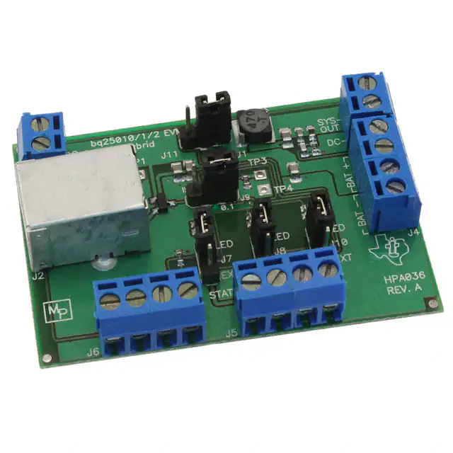
I/O Description
1.3
I/O Description
Jack
1.4
Description
J1-POS
AC adapter, positive output
J1-GND
AC adapter, negative output
J2
USB B-connector socket
J3-SYS-OUT
Positive output to system
J3-DC–
Negative output to system
J4-BAT+
Positive output to battery
J4-BAT–
Negative output to battery
J5-STAT1
STAT1 pin output voltage (when J7-2 and -3 are shorted)
J5-STAT2
STAT2 pin output voltage (when J8-2 and -3 are shorted)
J5-DC–
Connection to IC ground pin
J5-PG
PG pin output voltage (ac detection)
J7-LED
Power supply for LEDs, STAT1 monitoring
J7-EXT
STAT1 pin output voltage to external
J8-LED
Power supply for LEDs, STAT2 monitoring
J8-EXT
STAT2 pin output voltage to external
J10-LED
Power supply for LEDs, PG monitoring
J10-EXT
PG pin output voltage to external
Control and Key Parameter Settings
Jack or Resistor
1.5
Description
J6-CE
CE pin output voltage
Charge enabled
J6-ISET2
Charge current limit setting when charging from
USB
Set by J9
J6-DC–
Connection to IC ground pin
J6-EN
Enable input for dc-dc converter
Dc-dc converter enabled
J9
Charge current limit setting with USB input
1–2: 0.5 A
2–3: 0.1 A
2–3 (pins 2 and 3 are
shorted together)
J11
Forced PWM for dc-dc converter
1–2: forced PWM mode
2–3: power-save mode
2–3 (pins 2 and 3 are
shorted together)
R7
Charge current limit setting when charging from ac
adapter
1.62 kΩ (500 mA)
Recommended Operating Conditions
PARAMETER
MIN
NOM
VCC_USB
Supply voltage from USB input, maximum
ICC_AC
Supply current from ac adapter input, maximum
0.5
1.5
A
ICC_USB
Supply current from USB input, maximum (1)
100
500
mA
300
mA
125
°C
TJ
Operating junction temperature range
5
UNIT
Supply voltage from ac adapter input, maximum
(1)
(2)
4.5
MAX
VCC_AC
Dc-dc converter output current (2)
4
Factory Setting
4.35
0
–40
100
6.5
V
6.5
V
When using a USB port with the current limit less than 500mA, select 100mA charge rate using ISET2 pin (J9).
The typical current magnitude gives a 30% current ripple when using a 47-μH output inductor. The actual load current can be
higher or lower.
Introduction
SLUU214A – December 2004 – Revised June 2007
Submit Documentation Feedback
�www.ti.com
Recommended Output Inductor and Capacitor Values of the DC-DC Converter
1.6
Recommended Output Inductor and Capacitor Values of the DC-DC Converter
Part #
bq25010/15
DC-DC Converter
Output Voltage
0.7 V (1)
bq25011
or
bq25010/15
3.3 V (2)
bq25012/17
or
bq25010/15
1.8 V (3)
(1)
(2)
(3)
Converter Load
Current (mA)
Output
Inductance, L (μH)
Output
Capacitance, C
(μF)
Inductor Peak
Current (mA)
20
292–620
0.33–0.169
26–23
50
220
0.47
57.5
100
120
0.82
115
20
120
0.82
23
50
47
2.2
57.5
100
22
4.7
115
20
175
0.56
23
50
68
1.5
57.5
100
33
3.3
115
The product of output inductance L and capacitance C is recommended to be around 10-10 to better match the built-in
compensator.
The current ripple is recommended to be about 30% to achieve a high efficiency. Therefore, the inductance can be adjusted
according to the typical load current.
For bq25010, the output voltage is variable over a wide range. It may require a higher inductance for the worst case to maintain
30% current ripple. Depending on specific applications, an inductance with up to 60% current ripple may be acceptable.
SLUU214A – December 2004 – Revised June 2007
Submit Documentation Feedback
Introduction
5
�6
Introduction
SLUU214A – December 2004 – Revised June 2007
Submit Documentation Feedback
�Chapter 2
SLUU214A – December 2004 – Revised June 2007
Basic Functions Evaluation
2.1
Equipment
2.1.1 POWER SUPPLIES
Two power supplies capable of supplying 6 V at 1 A are required.
2.1.2 METERS
Three Fluke 75 (equivalent or better) or
Two equivalent voltmeters and an equivalent ammeter
2.1.3 OSCILLOSCOPE
An oscilloscope and a single voltage probe are required.
2.1.4 COMPUTER
A computer with at least one USB port and a USB cable
2.1.5 COMPONENTS
A 5-Ω, 50-W resistor
A 12-Ω, 0.5-W resistor
A 36-Ω, 0.25-W resistor
A 500-Ω, 0.25-W resistor
2.2
EQUIPMENT SETUP
The original test setup is shown in Figure 2-1.
1. Set power supply #1 for 5.0 ±0.1 VDC, 1.0 ±0.1-A current limit, and then turn off the supply. Connect
J1 (DC+, DC–) to power supply #1.
2. Plug one end of the USB cable into the computer USB port. Plug the other end into the USB input
socket J2 on the bqHYBRID EVM.
3. Connect the output of power supply #2 in series with a current meter (multimeter) to J4 (BAT+, BAT–).
4. Connect the 12-Ω, 0.5-W resistor across J3 (SYS, DC–).
5. Shunt jumpers should be installed on J7-LED, J8-LED, J9-0.1, and J10-LED, J11-1 (VBAT).
6. Short J6 pin 1 (EN) and pin 2 (DC–).
SLUU214A – December 2004 – Revised June 2007
Submit Documentation Feedback
Basic Functions Evaluation
7
�www.ti.com
PROCEDURE
Current
Meter
Power
Supply #1
bqHYBRID
EVM
AC
BAT+
(J1)
(J4)
Io
5W
50 W
Power
Supply #2
BAT–
Computer
USB
RL
12 W
0.5 W
SYS
(J3)
EN
B0235-01
Figure 2-1. Original Test Setup (Setup A)
2.3
PROCEDURE
1. Make sure the Equipment Setup steps are followed. Turn on power supply #2. Then turn on the
computer.
2. USB Input Precharge. Verify output voltage, BAT+, is about 2 VDC. Verify the red LED (D3) and
green LED (D2) are lit while the green LED (D4) is off. Verify IO, the output current from BAT+, is
between 40 mA and 60 mA.
3. USB Input Fast Charge. Increase the output voltage of power supply #2 slowly to 3.5 V. Verify the red
LED (D3) is on and the green LEDs (D2 and D4) are off. Verify IO is between 80 mA and 120 mA.
Verify the voltage of SYS (J3) is below 100 mV.
4. USB Input Sleep Mode. Increase the output voltage of power supply #2 slowly to 6 V. Verify both the
red LED (D3) and the green LED (D2) are off.
5. AC Adapter Input Precharge. Reduce the output voltage of power supply #2 slowly to 2 V. Turn on
power supply #1. Verify output voltage, BAT+, is about 2 VDC. Verify all the three LEDs (D3, D2, D4)
are lit. Verify IO, the output current from BAT+, is between 40 mA and 60 mA.
6. Disconnect USB cable from J2. Make sure the setup has been changed to that shown in Figure 2-2.
Current
Meter
bqHYBRID
EVM
BAT+
(J4)
Power
Supply #1
AC
(J1)
Io
5W
50 W
Power
Supply #2
BAT–
SYS
(J3)
EN
RL
12 W
0.5 W
B0235-02
Figure 2-2. Test Setup B
7. AC Adapter Input Fast Charge. Increase the output voltage of power supply #2 slowly to 3.5 V. Verify
the red LED (D3) and green LED (D4) are on and the green LED (D2) is off. Verify IO is between 450
mA and 550 mA (NOTE: If a Fluke 75 multimeter is used as the current meter, make sure the meter is
switched to A and the A socket is used instead of mA for this measurement). Verify the voltage of SYS
(J3) is below 100 mV.
8. AC Adapter Input Sleep Mode. Increase the output voltage of power supply #2 slowly to 6 V. Verify
both the red LED (D3) and the green LED (D2) are off.
9. DC-DC Converter Under Full-Load Condition (bq25012 as an Example). Increase the output
8
Basic Functions Evaluation
SLUU214A – December 2004 – Revised June 2007
Submit Documentation Feedback
�www.ti.com
PROCEDURE
voltage of power supply #2 slowly to 4.2 V. Disconnect J6 pin 1 (EN) from pin 2 (DC–). Make J6 pin 1
(EN) open. Verify the voltage across RL (SYS to DC–) is regulated between 1.75 V and 1.85 V. Verify
the voltage at the SW pin, or terminal 1 of L1, is like that shown in Figure 2-3. Verify that its frequency
is about 1 MHz and the duty cycle is stable at some value between 0.38 and 0.5.
G001
Figure 2-3. Waveform at Pin SW
10. DC-DC Converter Under Light-Load Condition (bq25012 as an Example). Change RL to the 36-Ω,
0.25-W resistor. Make sure the setup has been changed to that shown in Figure 2-4. Verify the voltage
across RL (SYS to DC–) is regulated between 1.75 V and 1.85 V. Verify the voltage at the SW pin, or
terminal 1 of L1, is like that shown in Figure 2-5. Verify that its frequency is about 1 MHz and the duty
cycle is stable at some value between 0.38 and 0.5.
Current
Meter
bqHYBRID
EVM
Io
VBAT
Power
Supply #1
5W
50 W
AC
SYS
EN
Power
Supply #2
RL
36 W
0.25 W
B0235-03
Figure 2-4. Test Setup C
SLUU214A – December 2004 – Revised June 2007
Submit Documentation Feedback
Basic Functions Evaluation
9
�www.ti.com
PROCEDURE
G002
Figure 2-5. Waveform at Pin SW
11. Converter Enable and Disable. Disconnect the current meter, the 5-Ω, 50-W resistor, and power
supply #2 from J4. Short J6 pin 1 (EN) and pin 2 (DC–). Verify the voltage of SYS (J3) is below 100
mV.
12. No Battery Load With DC-DC Converter Disabled, Switch From Charge to Charge Done to
Recharge, Back and Forth. Make sure the setup has been changed to setup D, as shown in
Figure 2-6. Verify that the LEDs, D3 and D2, alternate being lit. Measure the voltage at BAT+ with the
oscilloscope. Verify the waveform is like that in Figure 2-7. It is actually
Oscilloscope
bqHYBRID
EVM
BAT+
(J4)
Power
Supply #1
AC
(J1)
BAT–
SYS
(J3)
EN
RL
36 W
0.25 W
B0235-04
Figure 2-6. Test Setup D
10
Basic Functions Evaluation
SLUU214A – December 2004 – Revised June 2007
Submit Documentation Feedback
�www.ti.com
PROCEDURE
G003
Figure 2-7. BAT+ Waveform at No Load
13. No Battery; Charger Connected to System Directly. Connect the 500-Ω, 0.25-W resistor across J4
(BAT+ and BAT–). Make sure the test setup has been changed to setup E, as shown in Fig. 8. Verify
the red LED (D3) and green LED (D4) are on and the green LED (D2) is off. Verify the voltage across
BAT+ and BAT– is regulated between 4.160 V and 4.240 V.
bqHYBRID
EVM
BAT+
(J4)
Power
Supply #1
AC
(J1)
500 W
0.25 W
BAT–
SYS
(J3)
EN
RL
36 W
0.25 W
B0235-05
Figure 2-8. Test Setup E
SLUU214A – December 2004 – Revised June 2007
Submit Documentation Feedback
Basic Functions Evaluation
11
�12
Basic Functions Evaluation
SLUU214A – December 2004 – Revised June 2007
Submit Documentation Feedback
�Chapter 3
SLUU214A – December 2004 – Revised June 2007
Bill of Materials, Board Layout, and Schematic
3.1
Bill of Materials
bq2501x
RefDes
DESCRIPTION
MFR
Part Number
805
Panasonic
ECJ-2YB0J225K
Capacitor, ceramic, 10-μF,
6.3-V, X5R, 20%
805
Panasonic
ECJ-2FB0J106M
C4, C6
Capacitor, ceramic, 10-μF,
6.3-V, X5R, 20%
805
Panasonic
ECJ-2FB0J106M
0
C2
Capacitor, ceramic, 68 pF,
50-V, NPO
603
Panasonic
ECJ-1VC1H680J
1
0
C3
Capacitor, ceramic, 100-pF,
50-V, NPO
603
Panasonic
ECJ-1VC1H101J
1
1
1
C5
Capacitor, ceramic, 4.7-μF,
10-V, X5R, 10%
805
Panasonic
ECJ-2FB1A475K
1
1
1
1
D1
Diode, dual Schottky, 200-mA, SOT23
30-V
VishayLiteon
BAT54C
2
2
2
2
2
D2, D4
Diode, LED, green, 2.1-V,
20-mA, 6-mcd
603
Liteon
160-1183-1-ND
1
1
1
1
1
D3
Diode, LED, red, 1.8-V,
20-mA, 20-mcd
603
Liteon
160-1181-1-ND
2
2
2
2
2
J1, J3
Terminal block, 2-pin, 6-A,
3.5-mm
0.27 ×
0.25
OST
ED1514
1
1
1
1
1
J2
Connector, USB upstream
(type B)
0.47 ×
0.67
Molex
67068-1000
3
3
3
3
3
J4, J5,
J6
Terminal block, 4-pin, 6-A,
3.5-mm
0.55 ×
0.25
OST
ED1516
5
5
5
5
5
J7, J8,
J9, J10,
J11
Header, 3-pin, 100-mil
spacing, (36-pin strip)
0.100 × 3
Sullins
PTC36SAAN
5
5
5
5
5
--
Shunt, 100-mil, black
0.100
3M
929950-00
1
1
1
0
0
L1
Inductor, SMT, 47-μH, 0.48-A,
435-mΩ
0.185 ×
0.185
Sumida
CDRH4D28-470
0
0
0
1
1
L1
Inductor, SMT, 10-μH, 1-A,
95-mΩ
0.185 ×
0.185
Sumida
CDRH4D28-100
1
0
0
1
0
R1
Resistor, chip, 261-kΩ,
1/16-W, 1%
603
Std
Std
0
1
1
0
1
R1
Resistor, chip, 0-Ω, 1/16-W,
1%
603
Std
Std
1
0
0
1
0
R2
Resistor, chip, 100-kΩ,
1/16-W, 1%
603
Std
Std
1
1
1
1
1
R3
Resistor, chip, 100-kΩ,
1/16-W, 1%
603
Std
Std
1
1
1
1
1
R10
Resistor, chip, 10-kΩ, 1/16-W,
1%
603
Std
Std
x=0
-001
x=1
-002
x=2
-003
x=5
-004
x=7
-005
1
1
1
0
0
C1
Capacitor, ceramic, 2.2-μF,
6.3-V, X5R, 10%
0
0
0
1
1
C1
2
2
2
2
2
1
0
0
1
1
0
0
1
1
1
SLUU214A – December 2004 – Revised June 2007
Submit Documentation Feedback
SIZE
Bill of Materials, Board Layout, and Schematic
13
�www.ti.com
Board Layout
bq2501x
3.2
x=0
-001
x=1
-002
x=2
-003
x=5
-004
x=7
-005
RefDes
DESCRIPTION
SIZE
MFR
Part Number
3
3
3
3
3
R4, R5,
R6
Resistor, chip, 1.5-kΩ, 1/16-W, 603
1%
Std
Std
1
1
1
1
1
R7
Resistor, chip, 1.62-kΩ,
1/16-W, 1%
603
Std
Std
2
2
2
2
2
R8, R9
Resistor, chip, 1-kΩ, 1/16-W,
1%
603
Std
Std
1
0
0
0
0
U1
IC
QFN-20
TI
bq25010RHL
0
1
0
0
0
U1
IC
QFN-20
TI
bq25011RHL
0
0
1
0
0
U1
IC
QFN-20
TI
bq25012RHL
0
0
0
1
0
U1
IC
QFN-20
TI
bq25015RHL
0
0
0
0
1
U1
IC
QFN-20
TI
bq25017RHL
1
1
1
1
1
–
PCB, 2.3-in. × 2.2 in. × 0.031
in. (5.88-cm × 5.59-cm ×
0.787-mm)
Any
HPA036
Board Layout
2.210"
(56.134 mm)
1.520"
(38.608 mm)
K001
Figure 3-1. Top Assembly
14
Bill of Materials, Board Layout, and Schematic
SLUU214A – December 2004 – Revised June 2007
Submit Documentation Feedback
�www.ti.com
Board Layout
2.210"
(56.134 mm)
1.520"
(38.608 mm)
K003
Figure 3-2. Layer 1
2.210"
(56.134 mm)
1.520"
(38.608 mm)
K004
Figure 3-3. Layer 2
SLUU214A – December 2004 – Revised June 2007
Submit Documentation Feedback
Bill of Materials, Board Layout, and Schematic
15
�www.ti.com
Board Layout
Figure 3-4. Mask 1
Figure 3-5. Mask 2
2.210"
(56.134 mm)
1.520"
(38.608 mm)
K002
Figure 3-6. Silkscreen
16
Bill of Materials, Board Layout, and Schematic
SLUU214A – December 2004 – Revised June 2007
Submit Documentation Feedback
�www.ti.com
Schematic
Schematic
S001
3.3
Figure 3-7. Schematic Diagram
SLUU214A – December 2004 – Revised June 2007
Submit Documentation Feedback
Bill of Materials, Board Layout, and Schematic
17
�www.ti.com
Schematic
EVALUATION BOARD/KIT IMPORTANT NOTICE
Texas Instruments (TI) provides the enclosed product(s) under the following conditions:
This evaluation board/kit is intended for use for ENGINEERING DEVELOPMENT,
DEMONSTRATION, OR EVALUATION PURPOSES ONLY and is not considered by TI to be a
finished end-product fit for general consumer use. Persons handling the product(s) must have
electronics training and observe good engineering practice standards. As such, the goods being
provided are not intended to be complete in terms of required design-, marketing-, and/or
manufacturing-related protective considerations, including product safety and environmental
measures typically found in end products that incorporate such semiconductor components or
circuit boards. This evaluation board/kit does not fall within the scope of the European Union
directives regarding electromagnetic compatibility, restricted substances (RoHS), recycling
(WEEE), FCC, CE or UL, and therefore may not meet the technical requirements of these
directives or other related directives.
Should this evaluation board/kit not meet the specifications indicated in the User’s Guide, the
board/kit may be returned within 30 days from the date of delivery for a full refund. THE
FOREGOING WARRANTY IS THE EXCLUSIVE WARRANTY MADE BY SELLER TO BUYER
AND IS IN LIEU OF ALL OTHER WARRANTIES, EXPRESSED, IMPLIED, OR STATUTORY,
INCLUDING ANY WARRANTY OF MERCHANTABILITY OR FITNESS FOR ANY PARTICULAR
PURPOSE.
The user assumes all responsibility and liability for proper and safe handling of the goods. Further,
the user indemnifies TI from all claims arising from the handling or use of the goods. Due to the
open construction of the product, it is the user’s responsibility to take any and all appropriate
precautions with regard to electrostatic discharge.
EXCEPT TO THE EXTENT OF THE INDEMNITY SET FORTH ABOVE, NEITHER PARTY
SHALL BE LIABLE TO THE OTHER FOR ANY INDIRECT, SPECIAL, INCIDENTAL, OR
CONSEQUENTIAL DAMAGES.
TI currently deals with a variety of customers for products, and therefore our arrangement with the
user is not exclusive.
TI assumes no liability for applications assistance, customer product design, software
performance, or infringement of patents or services described herein.
Please read the User’s Guide and, specifically, the Warnings and Restrictions notice in the User’s
Guide prior to handling the product. This notice contains important safety information about
temperatures and voltages. For additional information on TI’s environmental and/or safety
programs, please contact the TI application engineer or visit www.ti.com/esh.
No license is granted under any patent right or other intellectual property right of TI covering or
relating to any machine, process, or combination in which such TI products or services might be
or are used.
FCC Warning
This evaluation board/kit is intended for use for ENGINEERING DEVELOPMENT,
DEMONSTRATION, OR EVALUATION PURPOSES ONLY and is not considered by TI to be a
finished end-product fit for general consumer use. It generates, uses, and can radiate radio
frequency energy and has not been tested for compliance with the limits of computing devices
pursuant to part 15 of FCC rules, which are designed to provide reasonable protection against
radio frequency interference. Operation of this equipment in other environments may cause
interference with radio communications, in which case the user at his own expense will be
required to take whatever measures may be required to correct this interference.
18
Bill of Materials, Board Layout, and Schematic
SLUU214A – December 2004 – Revised June 2007
Submit Documentation Feedback
�www.ti.com
Schematic
EVM WARNINGS AND RESTRICTIONS
It is important to operate this EVM within the charge regulation input voltage range of 4.35 V to
6.5 V and the adapter output voltage range of 0 V to 4.2 V.
Exceeding the specified input range may cause unexpected operation and/or irreversible damage
to the EVM. If there are questions concerning the input range, please contact a TI field
representative prior to connecting the input power.
Applying loads outside of the specified output range may result in unintended operation and/or
possible permanent damage to the EVM. Please consult the EVM User's Guide prior to
connecting any load to the EVM output. If there is uncertainty as to the load specification, please
contact a TI field representative.
During normal operation, some circuit components may have case temperatures greater than
60°C. The EVM is designed to operate properly with certain components above 60°C as long as
the input and output ranges are maintained. These components include but are not limited to
linear regulators, switching transistors, pass transistors, and current sense resistors. These types
of devices can be identified using the EVM schematic located in the EVM User's Guide. When
placing measurement probes near these devices during operation, please be aware that these
devices may be very warm to the touch.
Mailing Address: Texas Instruments, Post Office Box 655303, Dallas, Texas 75265
Copyright 2007, Texas Instruments Incorporated
SLUU214A – December 2004 – Revised June 2007
Submit Documentation Feedback
Bill of Materials, Board Layout, and Schematic
19
�IMPORTANT NOTICE
Texas Instruments Incorporated and its subsidiaries (TI) reserve the right to make corrections, modifications, enhancements,
improvements, and other changes to its products and services at any time and to discontinue any product or service without notice.
Customers should obtain the latest relevant information before placing orders and should verify that such information is current and
complete. All products are sold subject to TI’s terms and conditions of sale supplied at the time of order acknowledgment.
TI warrants performance of its hardware products to the specifications applicable at the time of sale in accordance with TI’s
standard warranty. Testing and other quality control techniques are used to the extent TI deems necessary to support this
warranty. Except where mandated by government requirements, testing of all parameters of each product is not necessarily
performed.
TI assumes no liability for applications assistance or customer product design. Customers are responsible for their products and
applications using TI components. To minimize the risks associated with customer products and applications, customers should
provide adequate design and operating safeguards.
TI does not warrant or represent that any license, either express or implied, is granted under any TI patent right, copyright, mask
work right, or other TI intellectual property right relating to any combination, machine, or process in which TI products or services
are used. Information published by TI regarding third-party products or services does not constitute a license from TI to use such
products or services or a warranty or endorsement thereof. Use of such information may require a license from a third party under
the patents or other intellectual property of the third party, or a license from TI under the patents or other intellectual property of TI.
Reproduction of TI information in TI data books or data sheets is permissible only if reproduction is without alteration and is
accompanied by all associated warranties, conditions, limitations, and notices. Reproduction of this information with alteration is an
unfair and deceptive business practice. TI is not responsible or liable for such altered documentation. Information of third parties
may be subject to additional restrictions.
Resale of TI products or services with statements different from or beyond the parameters stated by TI for that product or service
voids all express and any implied warranties for the associated TI product or service and is an unfair and deceptive business
practice. TI is not responsible or liable for any such statements.
TI products are not authorized for use in safety-critical applications (such as life support) where a failure of the TI product would
reasonably be expected to cause severe personal injury or death, unless officers of the parties have executed an agreement
specifically governing such use. Buyers represent that they have all necessary expertise in the safety and regulatory ramifications
of their applications, and acknowledge and agree that they are solely responsible for all legal, regulatory and safety-related
requirements concerning their products and any use of TI products in such safety-critical applications, notwithstanding any
applications-related information or support that may be provided by TI. Further, Buyers must fully indemnify TI and its
representatives against any damages arising out of the use of TI products in such safety-critical applications.
TI products are neither designed nor intended for use in military/aerospace applications or environments unless the TI products are
specifically designated by TI as military-grade or "enhanced plastic." Only products designated by TI as military-grade meet military
specifications. Buyers acknowledge and agree that any such use of TI products which TI has not designated as military-grade is
solely at the Buyer's risk, and that they are solely responsible for compliance with all legal and regulatory requirements in
connection with such use.
TI products are neither designed nor intended for use in automotive applications or environments unless the specific TI products
are designated by TI as compliant with ISO/TS 16949 requirements. Buyers acknowledge and agree that, if they use any
non-designated products in automotive applications, TI will not be responsible for any failure to meet such requirements.
Following are URLs where you can obtain information on other Texas Instruments products and application solutions:
Products
Applications
Amplifiers
amplifier.ti.com
Audio
www.ti.com/audio
Data Converters
dataconverter.ti.com
Automotive
www.ti.com/automotive
DSP
dsp.ti.com
Broadband
www.ti.com/broadband
Interface
interface.ti.com
Digital Control
www.ti.com/digitalcontrol
Logic
logic.ti.com
Military
www.ti.com/military
Power Mgmt
power.ti.com
Optical Networking
www.ti.com/opticalnetwork
Microcontrollers
microcontroller.ti.com
Security
www.ti.com/security
RFID
www.ti-rfid.com
Telephony
www.ti.com/telephony
Low Power
Wireless
www.ti.com/lpw
Video & Imaging
www.ti.com/video
Wireless
www.ti.com/wireless
Mailing Address: Texas Instruments, Post Office Box 655303, Dallas, Texas 75265
Copyright © 2007, Texas Instruments Incorporated
�