User's Guide
SLUU438 – July 2010
bq25050/bq25060EVM
This user's guide describes the features and operation of the bq25050/bq25060EVM Evaluation Module
(EVM). This EVM assists users in evaluating the bq25050 and bq25060 linear battery chargers. The
manual includes the bq25050/bq25060EVM bill of materials, board layout, and schematic.
1
2
3
4
5
6
Contents
Introduction .................................................................................................................. 2
1.1
EVM Features ...................................................................................................... 2
1.2
General Description ................................................................................................ 2
1.3
I/O Description ...................................................................................................... 2
1.4
Control and Key Parameters Setting ............................................................................ 3
1.5
Recommended Operating Conditions ........................................................................... 3
Equipment .................................................................................................................... 4
2.1
Power Supplies ..................................................................................................... 4
2.2
Loads ................................................................................................................ 4
2.3
Meters ............................................................................................................... 4
2.4
Computer and Interface ........................................................................................... 4
Equipment Setup ............................................................................................................ 4
Procedure .................................................................................................................... 6
4.1
Charger Operation with Minimum System Voltage Mode .................................................... 6
4.2
Input Current Setting .............................................................................................. 7
4.3
Charger Cut-Off by Thermistor ................................................................................... 7
PCB Layout Guideline ...................................................................................................... 8
Bill of Materials, Board Layout, and Schematics ........................................................................ 9
6.1
Bill of Materials ..................................................................................................... 9
6.2
Board Layout ...................................................................................................... 10
6.3
Schematic ......................................................................................................... 12
List of Figures
1
Original Test Setup for HPA577-001 – bq25050EVM.................................................................. 5
2
Original Test Setup for HPA577-002 – bq25060 EVM ................................................................. 5
3
Battery Load Circuit – Replacement for a Single Cell Li-Ion Battery → BAT+ to BAT– Voltage Tracks P/S
Input Voltage Minus 1 Diode Drop. ...................................................................................... 6
4
Top Layer ................................................................................................................... 10
5
Bottom Layer ............................................................................................................... 10
6
Top Assembly .............................................................................................................. 11
7
bq25050/60 EVM Schematic (Sheet 1 of 1) ........................................................................... 12
List of Tables
1
I/O Description............................................................................................................... 2
2
Control and Key Parameters Setting ..................................................................................... 3
3
Recommended Operating Conditions .................................................................................... 3
4
Bill of Materials .............................................................................................................. 9
SLUU438 – July 2010
bq25050/bq25060EVM
Copyright © 2010, Texas Instruments Incorporated
1
�Introduction
www.ti.com
1
Introduction
1.1
EVM Features
•
•
•
•
•
•
•
•
•
•
1.2
Evaluation module for bq25050/bq25060 (HPA577 E2)
30-V input rating, with 10.5-V overvoltage protection (OVP)
FET controller for external battery FET for external power path control (BGATE)
Programmable charge current
Input voltage dynamic power management
50-mA integrated low-dropout (LDO) linear regulator
Battery NTC monitoring during charge and discharge
Thermal regulation and protection.
Status indication – Charging/Done and Temperature Faults
Jumpers available. Easy-to-change connections.
General Description
The bq25050/60 is a highly integrated Li-Ion linear battery charger targeted at space-limited portable
applications. It operates from either a USB port or ac adapter and charges a single-cell Li-ion battery with
up to 1 A of charge current. The 30-V input voltage range with input overvoltage protections supports
low-cost unregulated adapters.
The bq25050/60 has a single power output that charges the battery. The system load is connected to
OUT. The low-battery system startup circuitry maintains OUT greater than 3.4 V whenever an input source
is connected. This allows the system to start up and run whenever an input source is connected
regardless of the battery voltage. The charge current is programmable up to 1 A using the ISET input.
Additionally, a 4.9-V, 50-mA LDO is integrated into the integrated circuit (IC) for supplying low power
external circuitry.
The battery is charged in three phases: conditioning, constant current, and constant voltage. In all charge
phases, an internal control loop monitors the IC junction temperature and reduces the charge current if an
internal temperature threshold is exceeded. The charger power stage and charge current sense functions
are fully integrated. The charger function has high accuracy current and voltage regulation loops, charge
status display, and charge termination.
For details, see the bq25050 (SLUSA33) and bq25060 (SLUSA32) data sheets.
1.3
I/O Description
Table 1. I/O Description
2
Jack
Description
J1–Vin
USB or ac adapter positive output
J1–GND
USB or ac adapter negative output
J2–OUT
Connected to system load
J2–GND
Ground
J3–BAT
Connected to battery pack
J3–GND
Ground
J3–GND
Ground
J3–TS
Temperature qualification voltage input
J4–VLDO
LDO output
J4–GND
Ground
J5
1-wire interface
JP1–Hi
Charge-enable active-HIGH logic input.
JP1–Ctrl (EN)
IC reference voltage VREF
JP1–Lo
Ground
bq25050/bq25060EVM
SLUU438 – July 2010
Copyright © 2010, Texas Instruments Incorporated
�Introduction
www.ti.com
Table 1. I/O Description (continued)
1.4
Jack
Description
JP2–TS
Battery pack NTC monitoring input
JP2–TSADJ
Onboard TS potentiometer
JP3–OUT
Connected to J2-OUT
JP3–BAT
Connected to J3-BAT
JP4–Vin
Connected to J1-Vin
JP4–R5
Connected to R5
JP5–LED
LED cathode
JP5–CHG
Charge status indicator open-drain output
JP6–BGATE
Battery P-channel MOSFET gate drive output
JP6–GND
Ground
Control and Key Parameters Setting
Table 2. Control and Key Parameters Setting
1.5
Jack
Description
Factory Setting
JP1
Ctrl (EN) pin setting
Connect Ctrl (EN) to Hi: Disables Chip
Float Ctrl (EN) pin: USB100 mode or Ctrl from J5 (-001)
Connect Ctrl (EN) to ground: ISET Ctrl
Float (No shunt) (-001)
Low (JP1:2-3) (-002)
JP2
TS setting
OFF: Connect TS to external battery pack NTC resistor
ON: Connect TS to onboard potentiometer
Jumper ON
JP3
OUT and BAT setting
OFF: Do not short OUT and BAT
ON: Short OUT and BAT
Jumper OFF
JP4
Onboard bias supply setting
Jumper ON
JP5
CHG LED setting
OFF: disconnect CHG and LED
ON: CHG
Jumper ON
JP6
BGATE setting
OFF: Enable BGATE
ON: Disable BGATE
Jumper OFF
Recommended Operating Conditions
Table 3. Recommended Operating Conditions
Symbol
Description
Min
Typ
Max
Unit
Supply voltage, VIN
Input voltage from ac adapter input
4.35
5
10.2
V
Battery voltage, VBAT
Voltage applied at VBAT terminal of J5
4.2
V
Supply current, IAC
Maximum input current from ac adapter
input
0
1
A
Charge current, Ichrg
Battery charge current
1
A
0
125
°C
Operating junction temperature
range, TJ
SLUU438 – July 2010
Notes
bq25050/bq25060EVM
Copyright © 2010, Texas Instruments Incorporated
3
�Equipment
2
Equipment
2.1
Power Supplies
www.ti.com
Power Supply 1 (PS#1): Adjustable from 0 to ≥ 5.1 Vdc at ≥ 1.5 A, use for input J1.
Power Supply 2 (PS#2): Adjustable from 0 to ≥ 5.1 Vdc at ≥ 2.5 A, used for Battery Load board.
2.2
Loads
Load #1: 25 Ω ±5%, ≥5 W.
Load #2: PR1010: Battery Load Circuit board, as shown in Figure 4.
LDO load: 1-kΩ resistor, 200 mW
2.3
Meters
Five Fluke 75 DMMs (equivalent or better).
2.4
Computer and Interface
A computer with at least one USB port.
HPA172, for -001 only.
3
Equipment Setup
The original test setup of HPA577-001 is shown in Figure 1.
The original test setup of HPA577-002 is shown in Figure 2.
1. Set the power supply #1 for 5.1 V ± 100 mVdc, 1.5 ±0.1-A current limit and then turn off supply.
2. Connect the output of power supply #1 in series with a current meter (multimeter) to J1 (VIN, GND).
3. Connect a voltage meter across J1 (VIN, GND).
4. Apply a 1-kΩ load resistor across J4 (VLDO, GND).
5. Connect Load #1 to J2 (OUT, GND).
6. Connect the Battery Load Circuit board to J3 (BAT, GND).
7. Set PS#2 to 2.3 Vdc ±100 mV and 2.5-A current limit, turn off and connect to the Battery Load Circuit
board.
8. Connect a voltage meter across J2 (OUT, GND).
9. Connect a voltage meter across J3 (BAT, GND).
10. Verify the shunts are placed correctly as per Table 2.
11. For HPA577-001 (bq25050 EVM) only:
Connect J5 to a computer with a USB Interface Adapter (HPA172).
The USB Interface Adapter software is available in the product folder at www.ti.com by searching for
the part number bq25050 and selecting the bq25050EVM link. A zip file under the Software and Tools
section can be downloaded. Extract the files onto the local hard drive, and double-click on the
bq25050.exe application evaluation file. A screen shot is shown in Figure 1.
4
bq25050/bq25060EVM
SLUU438 – July 2010
Copyright © 2010, Texas Instruments Incorporated
�Equipment Setup
www.ti.com
Iin
I
P/S#1
J5
-
JP4
JP
J1
VIN
GND
V
IN
1-wire
interface
JP5
LEDD1
/CH
IMON
(ISET) /CHG OUT
J2
OUT
V
GND
U1
J4
J3
JP3
VLDO
BAT
JP6 JP2
GND
V
GND
TS
bq25050/60 EVM
HPA577 Rev A
Load
#1
TS
Battery
Load
Circuit
#2
P/S#2
Figure 1. Original Test Setup for HPA577-001 – bq25050EVM
1-wire
interface
J5
JP
JP4
Power
supply #1
Iin
I
J1
VIN
GND
V
JP5
LEDD1
/CH
IMON
(ISET) /CHG OUT
IN
J2
OUT
GND
V
U
J4
J3
JP3
BAT
VLDO
GND
bq25050/60 EVM
HPA577 Rev A
JP6 JP2
TS
GND
TS
V
Load
#1
Battery
Load
Circuit
#2
P/S#2
Figure 2. Original Test Setup for HPA577-002 – bq25060 EVM
SLUU438 – July 2010
bq25050/bq25060EVM
Copyright © 2010, Texas Instruments Incorporated
5
�Procedure
www.ti.com
Figure 3. Battery Load Circuit – Replacement for a Single Cell Li-Ion Battery → BAT+ to BAT– Voltage
Tracks P/S Input Voltage Minus 1 Diode Drop.
4
Procedure
4.1
Charger Operation with Minimum System Voltage Mode
4.1.1
Turn on PS#1, preset to 5.1 Vdc
Measure → V(J4(VLDO)) = 4.9 ±100 mV
4.1.2
For -001: Trim R7, and set TS pin voltage to 0.5 V ± 50 mV. In the software window, click on
enable.
For -002: Trim R7 and set TS pin voltage to 1 V ±50 mV.
For -001 and -002: Turn on PS#2 set to 2.3 V ±50 mV.
Observe → D1(/CHG) on – This is precharge mode and OUT is held at its minimum system
voltage while the adapter is present and the battery below this minimum voltage. This
allows system power-up with a discharged battery.
Measure → Iin = 180 mA ±30 mA
Measure → V(J2(OUT)) = 3.5 V ±200 mV
4.1.3
Increase PS#2 to ~3.3 Vdc to raise VBAT to 3 V ±50 mV
Observe → D1(/CHG) on –This is fast-charge constant current mode and OUT is held at its
minimum system voltage while the adapter is present and the battery below this
minimum voltage. This allows system power-up with a discharged battery.
For -001 Measure → Iin = 285 mA ±50 mA
For -002 Measure → Iin = 467 mA ±50 mA
Measure → V(J2(OUT)) = 3.5 V ±200 mV.
4.1.4
Increase PS#2 to ~4.1Vdc to raise VBAT to 3.8 V ±50 mV.
Observe → D1(/CHG) on – This is fast-charge constant current mode and the battery is
above the minimum OUT voltage (with adapter present) so that the external BAT
FET is enabled, and Vout and Vbat track.
For -001 Measure → Iin = 285 mA ±50 mA
For -002 Measure → Iin = 467 mA ±50 mA
Measure → V(J2(OUT)) = 3.8 V ±200 mV
6
bq25050/bq25060EVM
SLUU438 – July 2010
Copyright © 2010, Texas Instruments Incorporated
�Procedure
www.ti.com
4.1.5
Increase PS#2 until D1 turns off indicating charger termination, to ~4.5 Vdc to raise VBAT to
~4.22 V.
Observe → D1(/CHG) off – Once terminated, the adapter powers the system. If the BAT pin is
driven too high in voltage by P/S#2, the battery overvoltage protection kicks in and
turns off the input FET, and the battery powers the system. This condition does not
normally occur with a battery in place of the battery bias circuit.
Measure → Iin = 180 mA ±50 mA
Measure → V(J2(OUT)) = 4.2 V ±200 mV
4.1.6
Decrease PS#2 to ~4.1 Vdc to lower VBAT to 3.8 V ±50 mV.
Observe → D1(/CHG) on – this shows refresh of the cell once some of the charge is
removed.
For -001 Measure → Iin = 285 mA ±50 mA
For -002 Measure → Iin = 467 mA ±50 mA
Measure → V(J2(OUT)) = 3.8 V ±200 mV
4.2
4.2.1
Input Current Setting
For HPA577-001 (bq25050 EVM) only:
In the software interface window, select 7 on "Number of Pulses," and click on "Send Pulses" to
bq25050EVM.
Measure → Iin = 374 mA ±50 mA
4.2.2
For HPA577-002 (bq25060 EVM) only:
PUT JP1 between EN and LO; trim R6 and observe the input current change.
Set → Iin = 374 mA ±50 mA
4.3
4.3.1
Charger Cut-Off by Thermistor
For HPA577-001 (bq25050 EVM) only:
Slowly trim R7 until V(J3(TS)) = 0.675 V ± 50 mV.
Observe → D1 (/CHG) flashing. This indicates a temperature fault that was tripped by the cold
temperature threshold comparator.
Trim R7 CW until V(J3(TS)) = 0.5 V ±50 mV.
Observe → D1 (/CHG) on.
Trim R7 CW until V(J3(TS)) = 0.75 V ±50 V.
Observe → D1 (/CHG) flashing. This indicates a temperature fault which was tripped by the hot
temperature threshold comparator.
SLUU438 – July 2010
bq25050/bq25060EVM
Copyright © 2010, Texas Instruments Incorporated
7
�PCB Layout Guideline
www.ti.com
Trim R2 CCW until V(J3(TS)) = 0.5 V ±50 mV.
Observe → D1 (/CHG) on.
4.3.2
For HPA577-002 (bq25060 EVM) only:
Slowly trim R7 until V(J3(TS)) = 1.30 V ±50 mV
Observe → D1 (/CHG) off. This indicates a temperature fault that was tripped by the cold
temperature threshold comparator
Trim R7 until V(J3(TS)) = 1 V ±50 mV.
Observe → D1 (/CHG) on.
Continue to trim R7 CW until V(J3(TS)) = 0.550 V ±50 mV
Observe → D1 (/CHG) off. This indicates a temperature fault that was tripped by the hot
temperature threshold comparator.
Trim R7 CCW until V(J3(TS)) = 1 V ± 50 mV.
Observe → D1 (/CHG) on.
5
PCB Layout Guideline
It is important to pay special attention to the printed-circuit board (PCB) layout. The following provides
some guidelines:
1. To obtain optimal performance, the decoupling capacitor from IN to GND (thermal pad) and the output
filter capacitors from OUT to GND (thermal pad) must be placed as close as possible to the
bq25050/60, with short trace runs to both IN, OUT, and GND (thermal pad).
2. All low-current GND connections must be kept separate from the high-current charge or discharge
paths from the battery. Use a single-point ground technique incorporating both the small signal ground
path and the power ground path.
3. The high current charge paths into IN pin and from the OUT pin must be sized appropriately for the
maximum charge current in order to avoid voltage drops in these traces.
4. The bq25050/60 is packaged in a thermally enhanced SON package. The package includes a thermal
pad to provide an effective thermal contact between the IC and the PCB; this thermal pad is also the
main ground connection for the device. Connect the thermal pad to the PCB ground connection. Full
PCB design guidelines for this package are provided in the application report entitled: QFN/SON PCB
Attachment Application Note (SLUA271).
8
bq25050/bq25060EVM
SLUU438 – July 2010
Copyright © 2010, Texas Instruments Incorporated
�Bill of Materials, Board Layout, and Schematics
www.ti.com
6
Bill of Materials, Board Layout, and Schematics
6.1
Bill of Materials
Table 4. Bill of Materials
Count
RefDes
Value
Description
Size
Part Number
MFR
2
C1, C5
0.1uF
Capacitor, Ceramic, 0.1-uF, 25-V, X7R, 10%
1206
Std
Std
1
C2
1uF
Capacitor, Ceramic, 1uF, 25-V, X7R, 10%
1206
Std
Std
1
1
C3
1uF
Capacitor, Ceramic, 1-uF, 6.3V, X5R, 20%
0805
Std
Std
1
1
C4
22uF
Capacitor, Ceramic, 22uF, 10V, X5R, 20%
1206
ECJ-HVB1A226M
Panasonic
2
2
C6, C7
0.1uF
Capacitor, Ceramic, 0.1uF, 25V, X7R, 10%
0603
Std
Std
0
0
C8
DNP
Capacitor, Ceramic, Low Inductance, vvV, [temp],
[tol]
0603
Std
Std
1
1
D1
Red
Diode, LED, Red, 1.8-V, 20-mA, 20-mcd
0603
LTST-C190CKT
Liteon
1
1
D2
BZX84C6v2T
Diode, Zener, 6.2-V, 350-mW
SOT-23
BZX84C6V2-7-F
Diodes
3
3
J1, J2, J4
ED1514
Terminal Block, 2-pin, 6-A, 3.5mm
0.27 x 0.25
ED555/2DS
OST
1
1
J3
ED555/4DS
Terminal Block, 4-pin, 6-A, 3.5mm
0.55 x 0.25 inch
ED555/4DS
OST
1
0
J5
Connector, Male Straight 2x5 pin, 100mil spacing,
4 Wall
0.338 x 0.788 inch
N2510-6002-UB
3M
1
1
JP1
PEC03SAAN
Header, Male 3-pin, 100mil spacing,
0.100 inch x 3
PEC03SAAN
Sullins
5
5
JP2, JP3,
JP4, JP5,
JP6
PEC02SAAN
Header, Male 2-pin, 100mil spacing,
0.100 inch x 2
PEC02SAAN
Sullins
1
1
Q1
NTR4101P
Trans, PChan FET -20V, 3.2A, Rds 0.070 Ohm
SOT-23
NTR4101PT1G
OnSemi
0
1
R1
24.3k
Resistor, Chip, 1/16W, 1%
0603
Std
Std
0
1
R2
11.3k
Resistor, Chip, 1/16W, 1%
0603
Std
Std
2
2
R3, R5
1k
Resistor, Chip, 1/16W, 1%
0603
Std
Std
1
1
R4
1.5k
Resistor, Chip, 1/16W, 1%
0603
Std
Std
1
1
R6
10k
Potentiometer, 1/4 in. Cermet, 12-Turn, Top-Adjust
0.25x0.17 inch
3266W-103LF
Bourns
1
1
R7
200k
Potentiometer, 1/4 Cermet, 12-Turn, Top-Adjust
0.25x0.17 inch
3266W-204LF
Bourns
1
0
R8
0
Resistor, Chip, 1/16W, 5%
0603
Std
Std
1
0
U1
BQ25050DQC
IC, 1A, Single-Input, Single Cell Li-Ion BATTERY
CHARGER with 50mA LDO and Minimum System
Voltage Support
TDFN-10
BQ25050DQC
TI
0
1
U1
BQ25060DQC
IC, 1A, Single-Input, Single Cell Li-Ion BATTERY
CHARGER with 50mA LDO and Minimum System
Voltage Support
TDFN-10
BQ25060DQC
TI
1
1
—
PCB, 2 In x 1.875 In x 0.031 In
HPA577
Any
6
6
—
Shunt, 100-mil, Black
929950-00
3M
-001
-002
2
1
SLUU438 – July 2010
0.100
bq25050/bq25060EVM
Copyright © 2010, Texas Instruments Incorporated
9
�Bill of Materials, Board Layout, and Schematics
6.2
www.ti.com
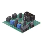
Board Layout
Figure 4. Top Layer
Figure 5. Bottom Layer
10
bq25050/bq25060EVM
SLUU438 – July 2010
Copyright © 2010, Texas Instruments Incorporated
�Bill of Materials, Board Layout, and Schematics
www.ti.com
Figure 6. Top Assembly
SLUU438 – July 2010
bq25050/bq25060EVM
Copyright © 2010, Texas Instruments Incorporated
11
�Bill of Materials, Board Layout, and Schematics
6.3
www.ti.com
Schematic
Figure 7. bq25050/60 EVM Schematic (Sheet 1 of 1)
12
bq25050/bq25060EVM
SLUU438 – July 2010
Copyright © 2010, Texas Instruments Incorporated
�Evaluation Board/Kit Important Notice
Texas Instruments (TI) provides the enclosed product(s) under the following conditions:
This evaluation board/kit is intended for use for ENGINEERING DEVELOPMENT, DEMONSTRATION, OR EVALUATION
PURPOSES ONLY and is not considered by TI to be a finished end-product fit for general consumer use. Persons handling the
product(s) must have electronics training and observe good engineering practice standards. As such, the goods being provided are
not intended to be complete in terms of required design-, marketing-, and/or manufacturing-related protective considerations,
including product safety and environmental measures typically found in end products that incorporate such semiconductor
components or circuit boards. This evaluation board/kit does not fall within the scope of the European Union directives regarding
electromagnetic compatibility, restricted substances (RoHS), recycling (WEEE), FCC, CE or UL, and therefore may not meet the
technical requirements of these directives or other related directives.
Should this evaluation board/kit not meet the specifications indicated in the User’s Guide, the board/kit may be returned within 30
days from the date of delivery for a full refund. THE FOREGOING WARRANTY IS THE EXCLUSIVE WARRANTY MADE BY
SELLER TO BUYER AND IS IN LIEU OF ALL OTHER WARRANTIES, EXPRESSED, IMPLIED, OR STATUTORY, INCLUDING
ANY WARRANTY OF MERCHANTABILITY OR FITNESS FOR ANY PARTICULAR PURPOSE.
The user assumes all responsibility and liability for proper and safe handling of the goods. Further, the user indemnifies TI from all
claims arising from the handling or use of the goods. Due to the open construction of the product, it is the user’s responsibility to
take any and all appropriate precautions with regard to electrostatic discharge.
EXCEPT TO THE EXTENT OF THE INDEMNITY SET FORTH ABOVE, NEITHER PARTY SHALL BE LIABLE TO THE OTHER
FOR ANY INDIRECT, SPECIAL, INCIDENTAL, OR CONSEQUENTIAL DAMAGES.
TI currently deals with a variety of customers for products, and therefore our arrangement with the user is not exclusive.
TI assumes no liability for applications assistance, customer product design, software performance, or infringement of
patents or services described herein.
Please read the User’s Guide and, specifically, the Warnings and Restrictions notice in the User’s Guide prior to handling the
product. This notice contains important safety information about temperatures and voltages. For additional information on TI’s
environmental and/or safety programs, please contact the TI application engineer or visit www.ti.com/esh.
No license is granted under any patent right or other intellectual property right of TI covering or relating to any machine, process, or
combination in which such TI products or services might be or are used.
FCC Warning
This evaluation board/kit is intended for use for ENGINEERING DEVELOPMENT, DEMONSTRATION, OR EVALUATION
PURPOSES ONLY and is not considered by TI to be a finished end-product fit for general consumer use. It generates, uses, and
can radiate radio frequency energy and has not been tested for compliance with the limits of computing devices pursuant to part 15
of FCC rules, which are designed to provide reasonable protection against radio frequency interference. Operation of this
equipment in other environments may cause interference with radio communications, in which case the user at his own expense
will be required to take whatever measures may be required to correct this interference.
EVM Warnings and Restrictions
It is important to operate this EVM within the input voltage range of 4.35 V to 10 V and the output voltage range of 0 V to 4.3 V .
Exceeding the specified input range may cause unexpected operation and/or irreversible damage to the EVM. If there are
questions concerning the input range, please contact a TI field representative prior to connecting the input power.
Applying loads outside of the specified output range may result in unintended operation and/or possible permanent damage to the
EVM. Please consult the EVM User's Guide prior to connecting any load to the EVM output. If there is uncertainty as to the load
specification, please contact a TI field representative.
During normal operation, some circuit components may have case temperatures greater than 60°C. The EVM is designed to
operate properly with certain components above 125°C as long as the input and output ranges are maintained. These components
include but are not limited to linear regulators, switching transistors, pass transistors, and current sense resistors. These types of
devices can be identified using the EVM schematic located in the EVM User's Guide. When placing measurement probes near
these devices during operation, please be aware that these devices may be very warm to the touch.
Mailing Address: Texas Instruments, Post Office Box 655303, Dallas, Texas 75265
Copyright © 2010, Texas Instruments Incorporated
�IMPORTANT NOTICE
Texas Instruments Incorporated and its subsidiaries (TI) reserve the right to make corrections, modifications, enhancements, improvements,
and other changes to its products and services at any time and to discontinue any product or service without notice. Customers should
obtain the latest relevant information before placing orders and should verify that such information is current and complete. All products are
sold subject to TI’s terms and conditions of sale supplied at the time of order acknowledgment.
TI warrants performance of its hardware products to the specifications applicable at the time of sale in accordance with TI’s standard
warranty. Testing and other quality control techniques are used to the extent TI deems necessary to support this warranty. Except where
mandated by government requirements, testing of all parameters of each product is not necessarily performed.
TI assumes no liability for applications assistance or customer product design. Customers are responsible for their products and
applications using TI components. To minimize the risks associated with customer products and applications, customers should provide
adequate design and operating safeguards.
TI does not warrant or represent that any license, either express or implied, is granted under any TI patent right, copyright, mask work right,
or other TI intellectual property right relating to any combination, machine, or process in which TI products or services are used. Information
published by TI regarding third-party products or services does not constitute a license from TI to use such products or services or a
warranty or endorsement thereof. Use of such information may require a license from a third party under the patents or other intellectual
property of the third party, or a license from TI under the patents or other intellectual property of TI.
Reproduction of TI information in TI data books or data sheets is permissible only if reproduction is without alteration and is accompanied
by all associated warranties, conditions, limitations, and notices. Reproduction of this information with alteration is an unfair and deceptive
business practice. TI is not responsible or liable for such altered documentation. Information of third parties may be subject to additional
restrictions.
Resale of TI products or services with statements different from or beyond the parameters stated by TI for that product or service voids all
express and any implied warranties for the associated TI product or service and is an unfair and deceptive business practice. TI is not
responsible or liable for any such statements.
TI products are not authorized for use in safety-critical applications (such as life support) where a failure of the TI product would reasonably
be expected to cause severe personal injury or death, unless officers of the parties have executed an agreement specifically governing
such use. Buyers represent that they have all necessary expertise in the safety and regulatory ramifications of their applications, and
acknowledge and agree that they are solely responsible for all legal, regulatory and safety-related requirements concerning their products
and any use of TI products in such safety-critical applications, notwithstanding any applications-related information or support that may be
provided by TI. Further, Buyers must fully indemnify TI and its representatives against any damages arising out of the use of TI products in
such safety-critical applications.
TI products are neither designed nor intended for use in military/aerospace applications or environments unless the TI products are
specifically designated by TI as military-grade or "enhanced plastic." Only products designated by TI as military-grade meet military
specifications. Buyers acknowledge and agree that any such use of TI products which TI has not designated as military-grade is solely at
the Buyer's risk, and that they are solely responsible for compliance with all legal and regulatory requirements in connection with such use.
TI products are neither designed nor intended for use in automotive applications or environments unless the specific TI products are
designated by TI as compliant with ISO/TS 16949 requirements. Buyers acknowledge and agree that, if they use any non-designated
products in automotive applications, TI will not be responsible for any failure to meet such requirements.
Following are URLs where you can obtain information on other Texas Instruments products and application solutions:
Products
Applications
Amplifiers
amplifier.ti.com
Audio
www.ti.com/audio
Data Converters
dataconverter.ti.com
Automotive
www.ti.com/automotive
DLP® Products
www.dlp.com
Communications and
Telecom
www.ti.com/communications
DSP
dsp.ti.com
Computers and
Peripherals
www.ti.com/computers
Clocks and Timers
www.ti.com/clocks
Consumer Electronics
www.ti.com/consumer-apps
Interface
interface.ti.com
Energy
www.ti.com/energy
Logic
logic.ti.com
Industrial
www.ti.com/industrial
Power Mgmt
power.ti.com
Medical
www.ti.com/medical
Microcontrollers
microcontroller.ti.com
Security
www.ti.com/security
RFID
www.ti-rfid.com
Space, Avionics &
Defense
www.ti.com/space-avionics-defense
RF/IF and ZigBee® Solutions www.ti.com/lprf
Video and Imaging
www.ti.com/video
Wireless
www.ti.com/wireless-apps
Mailing Address: Texas Instruments, Post Office Box 655303, Dallas, Texas 75265
Copyright © 2010, Texas Instruments Incorporated
�