bq25070
SLUSA66 – JULY 2011
www.ti.com
1A, Single-Input, Single-Cell LiFePO4 Linear Battery Charger with 50mA LDO
Check for Samples: bq25070
FEATURES
•
•
•
1
•
•
•
•
•
•
•
Single Cell LiFePO4 Charging Algorithm
30V Input Rating, With 10.5V Over-Voltage
Protection (OVP)
50mA Integrated Low Dropout Linear
Regulator (LDO)
Programmable Charge Current Through Single
Input Interface (CTRL)
7% Charge Current Regulation Accuracy
Thermal Regulation and Protection
Soft-Start Feature to Reduce Inrush Current
Battery NTC Monitoring
Charging Status Indication
Available in Small 2mm × 3mm 10 Pin SON
Package
APPLICATIONS
•
•
•
•
Smart Phones
Mobile Phones
Portable Media Players
Low Power Handheld Devices
DESCRIPTION
The bq25070 is a highly integrated LiFePO4 linear battery charger targeted at space-limited portable applications.
It operates from either a USB port or AC Adapter and charges a single-cell LiFePO4 battery with up to 1A of
charge current. The 30V input voltage range with input over-voltage protections supports low-cost unregulated
adapters.
The bq25070 has a single power output that charges the battery and powers the system. The charge current is
programmable up to 1A using the CTRL input. Additionally, a 4.9V ±10% 50mA LDO is integrated into the IC for
supplying low power external circuitry.
The LiFePO4 charging algorithm removes the constant voltage mode control usually present in Li-Ion battery
charge cycles. Instead, the battery is fastcharged to the overcharge voltage and then allowed to relax to a lower
float charge voltage threshold. The removal of the constant voltage control reduces charge time significantly.
During the charge cycle, an internal control loop monitors the IC junction temperature and reduces the charge
current if an internal temperature threshold is exceeded. The charger power stage and charge current sense
functions are fully integrated. The charger function has high accuracy current and voltage regulation loops, and
charge status display.
APPLICATION SCHEMATIC
bq25070
USB or TA
CHG
VBUS
GND
D+
VGPIO
R2
100 kW
STATUS
IN
VDD
OUT
C1
0.1 mF
C2
1 mF
D-
ABB
CTRL
BAT
PACK+
TEMP
TS
IMON
R1
1 kW
PACK-
GND
VCHG DET
LDO
PWRPD
C3
0.1 mF
R5
1.5 kW R3
1.5 kW
R4
1.5 kW
USB DET
VUSBIN
ACDET
GPIO
1
Please be aware that an important notice concerning availability, standard warranty, and use in critical applications of Texas
Instruments semiconductor products and disclaimers thereto appears at the end of this data sheet.
PRODUCTION DATA information is current as of publication date.
Products conform to specifications per the terms of the Texas
Instruments standard warranty. Production processing does not
necessarily include testing of all parameters.
Copyright © 2011, Texas Instruments Incorporated
�bq25070
SLUSA66 – JULY 2011
www.ti.com
These devices have limited built-in ESD protection. The leads should be shorted together or the device placed in conductive foam
during storage or handling to prevent electrostatic damage to the MOS gates.
ORDERING INFORMATION (1)
(1)
PART NUMBER
ILIM(DEF)
VBAT(OVCH)
VBAT(FLOAT)
VOVP
VLDO
MARKING
bq25070DQCR
300 mA
3.7 V
3.5 V
10.5 V
4.9 V
QUS
bq25070DQCT
300 mA
3.7 V
3.5 V
10.5 V
4.9 V
QUS
For the most current package and ordering information, see the Package Option Addendum at the end of this document, or visit the
device product folder on ti.com (www.ti.com),
ABSOLUTE MAXIMUM RATINGS (1)
over operating free-air temperature range (unless otherwise noted)
VALUE
UNIT
IN (with respect to GND)
–0.3 to 30
V
CTRL, TS (with respect to GND)
–0.3 to 7
V
Output Voltage
BAT, OUT, LDO, CHG, IMON (with respect to GND)
–0.3 to 7
V
Input Current (Continuous)
IN
1.2
A
Output Current (Continuous)
BAT
1.2
A
Output Current (Continuous)
LDO
100
mA
Output Sink Current
CHG
5
mA
Junction temperature, TJ
–40 to 150
°C
Storage temperature, TSTG
–65 to 150
°C
Input Voltage
(1)
Stresses beyond those listed under absolute maximum ratings may cause permanent damage to the device. These are stress ratings
only, and functional operation of the device at these or any other conditions beyond those indicated under recommended operating
conditions is not implied. Exposure to absolute-maximum-rated conditions for extended periods may affect device reliability. All voltage
values are with respect to the network ground terminal unless otherwise noted.
THERMAL INFORMATION
bq25070
THERMAL METRIC (1)
SON
UNITS
10 PINS
θJA
Junction-to-ambient thermal resistance (2)
58.7
θJCtop
Junction-to-case (top) thermal resistance (3)
3.9
(1)
(2)
(3)
°C/W
For more information about traditional and new thermal metrics, see the IC Package Thermal Metrics application report, SPRA953.
The junction-to-ambient thermal resistance under natural convection is obtained in a simulation on a JEDEC-standard, high-K board, as
specified in JESD51-7, in an environment described in JESD51-2a.
The junction-to-case (top) thermal resistance is obtained by simulating a cold plate test on the package top. No specific
JEDEC-standard test exists, but a close description can be found in the ANSI SEMI standard G30-88.
RECOMMENDED OPERATING CONDITIONS
MIN
VIN
IN voltage range
3.75
28
IN operating voltage range
3.75 (1)
10.2
IIN
Input current, IN
IOUT
Output Current in charge mode, OUT
TJ
Junction Temperature
(1)
2
MAX
(1)
1
0
UNITS
V
A
1
A
125
°C
Charge current may be limited at low input voltages due to the dropout of the device.
Copyright © 2011, Texas Instruments Incorporated
�bq25070
SLUSA66 – JULY 2011
www.ti.com
ELECTRICAL CHARACTERISTICS
Over junction temperature range 0°C ≤ TJ ≤ 125°C and recommended supply voltage (unless otherwise noted)
PARAMETER
TEST CONDITIONS
MIN
TYP
MAX
3.15
3.30
3.55
UNITS
INPUT
VUVLO
Under-voltage lock-out
VIN: 0 V → 4 V
VHYS-UVLO
Hysteresis on UVLO
VIN: 4 V → 0 V
VBATUVLO
Battery UVLO
VBAT rising
VHYS-BUVLO
Hysteresis on BAT UVLO
VBAT falling
VIN-SLP
Valid input source threshold VIN-SLP above
VBAT
Input power good if VIN > VBAT +
VIN-SLP
VBAT = 3.6 V, VIN: 3.5 V → 4 V
30
75
150
mV
VHYS-INSLP
Hysteresis on VIN-SLP
VBAT = 3.6 V, VIN: 4 V → 3.5 V
18
32
54
mV
tDGL(NO-IN)
Delay time, input power loss to charger
turn-off
Time measured from VIN: 5 V → 2.5 V
1μs fall-time
VOVP
Input over-voltage protection threshold
VIN: 5 V → 11 V
VHYS-OVP
Hysteresis on OVP
VIN: 11 V → 5 V
tBLK(OVP)
Input over-voltage blanking time
tREC(OVP)
Input over-voltage recovery time
250
1.95
2.05
2.15
125
10.5
V
mV
32
10.2
V
mV
ms
10.8
V
100
mV
100
μs
Time measured from VIN: 11 V → 5 V
1μs fall-time to LDO = HI, VBAT = 3.5 V
100
μs
VIN = 0 V, VCHG = High, TS Enabled
120
QUIESCENT CURRENT
IBAT(PDWN)
IIN(STDBY)
ICC
Battery current into BAT, No input connected
Standby current into IN pin
Active supply current, IN pin
VIN = 0 V, VCHG = Low, TS Disabled,
TJ = 85°C
150
μA
6
μA
CTRL = HI, VIN = 5.5V
0.25
CTRL = HI, VIN ≤ VOVP
0.5
CTRL = HI, VIN > VOVP
2
VIN = 6 V, No load on OUT pin,
VBAT> VBAT(REG), IC enabled
3
mA
mA
BATTERY CHARGER FAST-CHARGE
VBAT(REG)
Battery float charge voltage
VBAT(OVCH)
Battery overcharge voltage threshold
IIN(LIM)
Input Current Limit (selected by CTRL
interface)
TA = 0°C to 125°C
3.465
3.5
3.535
TA = 25°C
3.465
3.5
3.529
3.62
3.7
3.78
4 pulses on CTRL
87
93
100
5 pulses on CTRL
174
187
200
6 pulses on CTRL
261
280
300
7 pulses on CTRL
348
374
400
8 pulses on CTRL
435
467
500
9 pulses on CTRL
608
654
700
10 pulses on CTRL
739
794
850
11 pulses on CTRL
869
935
1000
500
1400
VDO(IN-OUT)
VIN – VOUT
VIN = 3.5 V, IOUT = 0.75 A
KIMON
Input current monitor ratio
KIMON = IIMON / ICHG, RIMON = 1kΩ,
Current programmed using CTRL
VIMON(MAX)
Maximum IMON voltage
IMON open
IMON Accuracy
1
1.2
V
V
mA
mV
mA / A
1.25
IIN < 100 mA
–25%
25%
IIN = 100 mA to 1 A
–10%
10%
V
PRE-CHARGE AND CHARGE DONE
VLOWV
Pre-charge to fast-charge transition threshold
tDGL1(LOWV)
Deglitch time on pre-charge to fast-charge
transition
25
ms
tDGL2(LOWV)
Deglitch time on fast-charge to pre-charge
transition
25
ms
Copyright © 2011, Texas Instruments Incorporated
2.4
2.5
2.6
V
3
�bq25070
SLUSA66 – JULY 2011
www.ti.com
ELECTRICAL CHARACTERISTICS (continued)
Over junction temperature range 0°C ≤ TJ ≤ 125°C and recommended supply voltage (unless otherwise noted)
PARAMETER
IPRECHARGE
Precharge current to BAT during precharge
mode
TEST CONDITIONS
VBAT = 0 V to 0.7 V
MIN
TYP
MAX
UNITS
41.5
45
48.5
mA
3.1
3.3
3.5
V
RECHARGE OR REFRESH
VRCH
Recharge detection threshold
VBAT falling
tDGL(RCH)
Deglitch time, recharge threshold detected
VBAT falling to New Charge Cycle
VLDO
LDO Output Voltage
VIN = 5 V to 10.5 V,
ILDO = 0 mA to 50 mA
ILDO
Maximum LDO Output Current
VDO
Dropout Voltage
25
ms
LDO
4.7
4.9
5.1
200
350
60
VIN = 4.5V, ILDO = 50mA
V
mA
mV
CTRL INTERFACE
tCTRL_DGL
CTRL Deglitch timer
5
tCTRL_LATCH
CTRL Latch timer
2
tHI_MIN
High Duration on CTRL
50
tLO_MIN
Low Time Duration on CTRL
50
RPULLDOWN
CTRL Pulldown Resistor
ms
ms
1000
1000
260
μs
μs
kΩ
LOGIC LEVELS ON CTRL
VIL
Logic LOW input voltage
VIH
Logic HIGH input voltage
0.4
1.4
V
V
BATTERY-PACK NTC MONITOR (TS)
VCOLD
TS Cold Threshold
VTS Rising
24.5
25
12
12.5
25.5
VCUTOFF
TS Cold Cutoff Threshold
VTS Falling
VHOT
TS Hot Threshold
VTS Falling
VHOT_HYS
TS Hot Cutoff Threshold
VTS Rising
tdgl(TS)
Deglitch for TS Fault
Fault detected on TS to stop charge
VOL
Output LOW voltage
ISINK = 1 mA
IIH
Leakage current
CHG = 5 V
tFLSH(TS)
TS fault flash period
50% Duty Cycle, TS out of valid range
100
ms
1
%VLDO
%VLDO
13
%VLDO
1
%VLDO
25
ms
CHG OUTPUT
0.45
1
V
μA
THERMAL REGULATION
TJ(REG)
Temperature Regulation Limit
TJ rising
125
C
TJ(OFF)
Thermal shutdown temperature
TJ rising
155
C
TJ(OFF-HYS)
Thermal shutdown hysteresis
TJ falling
20
C
4
Copyright © 2011, Texas Instruments Incorporated
�bq25070
SLUSA66 – JULY 2011
www.ti.com
TYPICAL CHARACTERISTICS
VIN = 5 V, VBAT = 3.2 V, ICHG = 280 mA, Typical Application Circuit
5V/div
VCTRL
5V/div
VIN
5V/div
VLDO
5V/div
VLDO
200mA/div
200mA/div
IOUT
IOUT
2V/div
2V/div
VCHG
VCHG
VCTRL = 0V
10ms/div
20ms/div
G002
G001
Figure 1. Adapter Plug-In With Battery Connected
Figure 2. Charger Enable Using CTRL
5V/div
VCTRL
2V/div
5V/div
VLDO
VCTRL
200mA/div
IOUT
500mA/div
2V/div
VCHG
IOUT
400μs/div
4ms/div
G003
Figure 3. Charger Disable Using CTRL
G004
Figure 4. Default to 1A Transition Using CTRL
VIN = 5V to 12V
5V/div
VIN
5V/div
VLDO
1A/div
IOUT
2V/div
VCHG
40μs/div
G005
Figure 5. OVP Fault
Copyright © 2011, Texas Instruments Incorporated
5
�bq25070
SLUSA66 – JULY 2011
www.ti.com
TYPICAL CHARACTERISTICS (continued)
VIN = 5 V, VBAT = 3.2 V, ICHG = 280 mA, Typical Application Circuit
VOLTAGE and CURRENT
vs
ELAPSED TIME
4
1.6
3.5
1.4
1.2
1
2.5
2
0.8
1.5
0.6
1
0.4
0.5
0.2
1.5
1.4
1.3
1.2
1.1
1
0.9
0.8
0.7
0.6
0.5
0.4
0.3
0.2
0.1
0
25
50
75
Temperature (°C)
Figure 7.
BATTERY REGULATION VOLTAGE
vs
CHARGE CURRENT
OVP THRESHOLD
vs
TEMPERATURE
3.54
10.58
3.53
10.56
3.52
3.51
3.5
3.49
3.48
10.5
10.46
10.42
0.3
0.4 0.5 0.6 0.7
Charge Current (A)
0.8
0.9
10.4
1
G007
10.48
10.44
0.2
125
10.52
3.46
0.1
100
10.54
3.47
1.1
1.05
1
0.95
0.9
0.85
0.8
0.75
0.7
0.65
0.6
0.55
0.5
0.45
0.4
0
Figure 6. Complete Charge Cycle
10.6
0
VIN = 4.5V
IOUT = 1A
G006
3.55
3.45
Charge Current (A)
0
4:48:00
1:12:00
2:24:00
3:36:00
Elapsed Time (hh:mm:ss)
OVP Threshold (V)
Battery Regulation Voltage (V)
0
0:00:00
Dropout Voltage (V)
IBAT
0
25
50
75
Temperature (°C)
G008
100
125
G009
Figure 8.
Figure 9.
CHARGE CURRENT
vs
INPUT VOLTAGE
INPUT CURRENT LIMIT
vs
BATTERY VOLTAGE
0.7
0.6
Input Current Limit (A)
Voltage (V)
VCHG
Current (A)
VBAT
3
Thermal
Regulation
VIN = 5V
100mA Current Limit
500mA Current Limit
0.5
0.4
0.3
0.2
0.1
5
6
7
8
Input Voltage (V)
Figure 10.
6
DROPOUT VOLTAGE
vs
TEMPERATURE
9
10
G010
0
2.5
2.75
3
Battery Voltage (V)
3.25
3.5
G011
Figure 11.
Copyright © 2011, Texas Instruments Incorporated
�bq25070
SLUSA66 – JULY 2011
www.ti.com
SIMPLIFIED BLOCK DIAGRAM
LDO
+
–
Q1
Q2
IN
OUT
+
Charge
Pump
IMON
–
125°C
TJ
IIN(REG)
1.5V
BAT
–
+
VBAT(REG)
–
+
VREF
Charge
Pump
ILIM
Overcharge Comparator
VBAT
–
3.7V
+
Sleep Comparator
CTRL
260kΩ
VLDO
OVP Comparator
+
VOVP
–
VIN
Charge
Control
–
75mV
VBAT
+
Digital
Decode
VIN
CHG
Status
Output
Disable
+
TS Cold
–
+
TS Hot
–
TS
GND
Copyright © 2011, Texas Instruments Incorporated
7
�bq25070
SLUSA66 – JULY 2011
www.ti.com
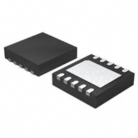
PIN CONFIGURATION
(Top View)
IN
1
10
OUT
IMON
2
9
GND
GND
3
8
CHG
bq25070
LDO
4
7
CTRL
TS
5
6
BAT
10 -pin 2mm x 3mm DFN
PIN FUNCTIONS
PIN
NAME
NO.
I/O
DESCRIPTION
IN
1
I
Input power supply. IN is connected to the external DC supply (AC adapter or USB port). Bypass IN to GND
with at least a 0.1μF ceramic capacitor.
IMON
2
O
Current monitoring output. Connect a 1kΩ resistor from IMON to GND to monitor the input current. The
voltage at IMON ranges from 0V to 1V which corresponds to an input current from 0A to 1A.
GND
3, 9
–
Ground terminal. Connect to the thermal pad and the ground plane of the circuit.
LDO
4
O
LDO output. LDO is regulated to 4.9V and drives up to 50mA. Bypass LDO to GND with a 0.1μF ceramic
capacitor. LDO is enabled when VUVLO < VIN < VOVP.
TS
5
I
Battery pack NTC monitoring input. Connect a resistor divider from LDO to GND with TS connected to the
center tap to set the charge temperature window. The battery pack NTC is connected in parallel with the
bottom resistor of the divider. See the Applications Design section for details on the selecting the proper
component values.
BAT
6
O
Battery connection output. BAT is the sense input for the battery. Connect BAT and OUT to the battery and
bypass to GND with a 1μF ceramic capacitor.
CTRL
7
I
Single-input interface Input. Drive CTRL with pulses to enable/disable the device, enable/disable VIN-DPM,
and select current limits. See the interface section for details on using the CTRL interface.
CHG
8
O
Charge status indicator open-drain output. CHG is pulled low while the device is charging the battery. CHG
goes high impedance when the battery is fully charged.
OUT
10
O
System output connection. Connect OUT and BAT together. Bypass the OUT and BAT connection to GND
with a 1μF ceramic capacitor.
Pad
–
There is an internal electrical connection between the exposed thermal pad and the GND pin of the device.
The thermal pad must be connected to the same potential as the GND pin on the printed circuit board. Do not
use the thermal pad as the primary ground input for the device. GND pin must be connected to ground at all
times.
Thermal
PAD
8
Copyright © 2011, Texas Instruments Incorporated
�bq25070
SLUSA66 – JULY 2011
www.ti.com
APPLICATIONS CIRCUITS
VGPIO
R2
100 kW
USB or TA
STATUS
CHG
IN
VBUS
GND
OUT
C1
0.1 mF
D+
D-
VDD
C2
1 mF
ABB
bq25070
CTRL
BAT
PACK+
TEMP
TS
IMON
R1
1 kW
PACK-
GND
VCHG DET
LDO
PWRPD
C3
0.1 mF
R5
1.5 kW
USB DET
R3
1.5 kW
R4
1.5 kW
VUSBIN
ACDET
GPIO
Figure 12. bq25070 Typical Application Circuit
Copyright © 2011, Texas Instruments Incorporated
9
�bq25070
SLUSA66 – JULY 2011
www.ti.com
DETAILED FUNCTIONAL DESCRIPTION
The bq25070 is a highly integrated LiFePO4 linear battery charger targeted at space-limited portable applications.
It operates from either a USB port or AC Adapter and charges a single-cell LiFePO4 battery with up to 1A of
charge current. The 30V input voltage range with input over-voltage protections supports low-cost unregulated
adapters.
The LiFePO4 charging algorithm removes the constant voltage mode control usually present in Li-Ion battery
charge cycles. Instead, the battery is charged with the fastcharge current to the overcharge voltage and then
allowed to relax to a lower float charge voltage threshold. The removal of the constant voltage control reduces
charge time significantly. During the charge cycle, an internal control loop monitors the IC junction temperature
and reduces the charge current if an internal temperature threshold is exceeded. The charger power stage and
charge current sense functions are fully integrated. The charger function has high accuracy voltage and current
regulation loops, and charge status display.
CHARGING OPERATION
The bq25070 uses a charge algorithm that is unique to LiFePO4 chemistry cells. The constant voltage mode
control usually present in Li-Ion battery charge cycles is eliminated. This dramatically decreases the charge time.
When the bq25070 is enabled by CTRL, the battery voltage is monitored to verify which stage of charging must
be used. When VBAT < VLOWV, the bq25070 charges in precharge mode; when VBAT > VLOWV, the normal charge
cycle is used.
Charger Operation with Minimum System Voltage Mode Enabled
PRECHARGE
Constant Current
Fast Charge
Float-Voltage
Regulation
VOUT(OVCH)
VOUT(REG)
IFASTCHG
CHG = Hi -Z
VLOWV
IPRECHG
Battery and
Output
Voltage
Battery
Current
Figure 13. Typical Charging Cycle with Minimum System Voltage Enabled
Precharge Mode (VBAT ≤ VLOWV)
The bq25070 enters precharge mode when VBAT ≤ VLOWV. Upon entering precharge mode, the battery is charged
with a 47.5mA current and CHG goes low.
10
Copyright © 2011, Texas Instruments Incorporated
�bq25070
SLUSA66 – JULY 2011
www.ti.com
Fast Charge Mode
Once VBAT > VLOWV, the bq25070 enters constant current (CC) mode where charge current is regulated using the
internal MOSFETs between IN and OUT. The total current is shared between the output load and the battery.
Once the battery voltage charges up to VBAT(OVCH), the CHG output goes high indicating the charge cycle is
complete and the bq25070 switches the battery regulation voltage to VBAT(REG). The battery voltage is allowed to
relax down to VBAT(REG). The charger remains enabled and regulates the output to VBAT(REG). If at any time the
battery falls below VREC, the charge cycle restarts.
CHARGE CURRENT TRANSLATOR (IMON)
When the charger is enabled, internal circuits generate a current proportional to the charge current at the IMON
input. The current out of IMON is 1/1000 (±10%) of the charge current. This current, when applied to the external
charge current programming resistor, R1 (Figure 12), generates an analog voltage that can be monitored by an
external host to calculate the current sourced from BAT. Connect a 1kΩ resistor from IMON to GND. The voltage
at IMON is calculated as:
VIMON = IIN ´ 1 V
A
(1)
INPUT OVER VOLTAGE PROTECTION
The bq25070 contains an input over voltage protection circuit that disables the LDO output and charging when
the input voltage rises above VOVP. This prevents damage from faulty adapters. The OVP circuitry contains an
115μs deglitch that prevents ringing on the input from line transients from tripping the OVP circuitry falsely. If an
adapter with an output greater than VOVP is plugged in, the IC completes soft-start power up and then shuts
down if the voltage remains above VOVP after 115μs. The LDO remains off and charging remains disabled until
the input voltage falls below VOVP.
UNDER-VOLTAGE LOCKOUT (UVLO)
The bq25070 remains in power down mode when the input voltage is below the under-voltage lockout threshold
(VUVLO). During this mode, the control input (CTRL) is ignored. The LDO, the charge FET connected between IN
and OUT are off and the status output (CHG) is high impedance. Once the input voltage rises above VUVLO, the
internal circuitry is turned on and the normal operating procedures are followed.
EXTERNAL NTC MONITORING (TS)
The bq25070 features a flexible, voltage based external battery pack temperature monitoring input. The TS input
connects to the NTC thermistor in the battery pack to monitor battery temperature and prevent dangerous
over-temperature conditions. During charging, the voltage at TS is continuously monitored. If, at any time, the
voltage at TS is outside of the operating range (VCOLD to VHOT), charging is suspended. When the voltage
measured at TS returns to within the operation window, charging is resumed. When charging is suspended due
to a battery pack temperature fault, the CHG output remains low and continues to indicate charging.
The temperature thresholds are programmed using a resistor divider from LDO to GND with the NTC thermistor
connected to the center tap from TS to GND. See Figure 14 for the circuit example. The value of R1 and R2 are
calculated using the following equations:
-R2 ´ RHOT ´ (0.125 - 1)
R1 =
0.125 ´ (R2 + RHOT)
(2)
R2 =
-RHOT ´ RCOLD ´ (0.125 - 0.250)
RHOT ´ 0.250 ´ (0.125 - 1) + RCOLD ´ 0.125 ´ (1 - 0.250)
(3)
RHOT is the expected thermistor resistance at the programmed hot threshold; RCOLD is the expected thermistor
resistance at the programmed cold threshold.
Copyright © 2011, Texas Instruments Incorporated
11
�bq25070
SLUSA66 – JULY 2011
www.ti.com
LDO
R1
VCOLD
TS
PACK+
TEMP
+
VHOT
R2
PACK-
+
bq25070
For applications that do not require the TS monitoring function, set R1 = 490kΩ and R2 = 100kΩ to set the TS voltage
at a valid level and maintain charging.
Figure 14. NTC Monitoring Function
50 mA LDO (LDO)
The LDO output of the bq25070 is a low dropout linear regulator (LDO) that supplies up to 50mA while regulating
to VLDO. The LDO is active whenever the input voltage is above VUVLO and below VOVP. It is not affected by the
CTRL input. The LDO output is used to power and protect circuitry such as USB transceivers from transients on
the input supply.
CHARGE STATUS INDICATOR (CHG)
The bq25070 contains an open drain CHG output that indicates when charge cycles and faults. When charging a
battery in precharge or fastcharge mode, the CHG output is pulled to GND. Once the BAT output reaches the
overcharge voltage threshold, CHG goes high impedance to signal the battery is fully charged. The CHG output
goes low during battery recharge cycles to signal the host.
Additionally, CHG notifies the host if a NTC temperature fault has occurred. CHG pulses with a period of 100ms
and a 50% duty cycle if a TS faults occurs. Connect CHG to the required logic level voltage through a 1kΩ to
100kΩ resistor to use the signal with a microprocessor. ICHG must be below 5mA.
The IC monitors the CHG pin when no input is connected to verify if the system circuitry is active. If the voltage
at CHG is logic being drive low when no input is connected, the TS circuit is turned off for a low quiescent current
state. Once the voltage at CHG increases above logic high, the TS circuit is turned on.
SINGLE INPUT INTERFACE (CTRL)
CTRL is used to enable/disable the device as well as select the input current limit, enable/disable charge, extend
the TS operation range and disable VIN-DPM mode. CTRL is pulled low to enable the device. After the 50μs
deglitch expires, the IC enters the 32ms WAIT state. CTRL may be used to program the bq25070 during this
time. Once tWAIT expires, the IC starts up. If no command is sent to CTRL during tWAIT, the IC starts up with a
default 285mA current limit.
Programming the different modes is done by pulsing the CTRL input. See Table 1 for a map of the different
modes. The width of the CTRL pulses is unimportant as long as they are between 50μs and 1000μs long. The
time between pulses must be between 50μs and 1000μs to be properly read. Once CTRL is held low for 2ms,
the number of pulses is passed to the control logic and decoded and then the mode changes. To ensure proper
operation, do not send more than 16 pulses in one programming cycle.
12
Copyright © 2011, Texas Instruments Incorporated
�bq25070
SLUSA66 – JULY 2011
www.ti.com
Table 1. Pulse Counting Map for CTRL Interface
# of Pulses
Current Limit
1
No Change
2
No Change
3
No Change
4
93 mA
5
187 mA
6
280 mA
7
374 mA
8
467 mA
9
654 mA
10
794 mA
11
935 mA
>11
No Change
If, at any time, the CTRL input is held high for more than 2ms, the IC is disabled. When disabled, charging is
suspended and the bq25070 input quiescent current is reduced.
IC disabled if CTRL
pulled high for >2.0ms
# of pulses decoded once
CTRL pulled low for 2.0ms
IC can be
programmed during
tWAIT
tHI
2.0ms
2.0ms
CTRL
tCTRL_DGL
tCTRL_LATCH
2.0ms
tCTRL_LATCH
tCTRL_LATCH
tLO
Power up with default
285mA current limit
475mA current limit
programmed
190mA current limit
programmed
IIN
Figure 15. CTRL Timing Diagram
THERMAL REGULATION AND THERMAL SHUTDOWN
The bq25070 contains a thermal regulation loop that monitors the die temperature continuously. If the
temperature exceeds TJ(REG), the device automatically reduces the charging current to prevent the die
temperature from increasing further. In some cases, the die temperature continues to rise despite the operation
of the thermal loop, particularly under high VIN conditions. If the die temperature increases to TJ(OFF), the IC is
turned off. Once the device die temperature cools by TJ(OFF-HYS), the device turns on and returns to thermal
regulation. Continuous over-temperature conditions result in the pulsing of the load current. If the junction
temperature of the device exceeds TJ(OFF), the charge FET is turned off. The FET is turned back on when the
junction temperature falls below TJ(OFF) – TJ(OFF-HYS).
Note that these features monitor the die temperature of the bq25070. This is not synonymous with ambient
temperature. Self heating exists due to the power dissipated in the IC because of the linear nature of the battery
charging algorithm.
Copyright © 2011, Texas Instruments Incorporated
13
�bq25070
SLUSA66 – JULY 2011
www.ti.com
APPLICATION INFORMATION
SELECTION OF INPUT/OUTPUT CAPACITORS
In most applications, all that is needed is a high-frequency decoupling capacitor on the input power pin. For
normal charging applications, a 0.1μF ceramic capacitor, placed in close proximity to the IN pin and GND pad
works best. In some applications, depending on the power supply characteristics and cable length, it may be
necessary to increase the input filter capacitor to avoid exceeding the OVP voltage threshold during adapter hot
plug events where the ringing exceeds the deglitch time.
The charger in the bq25070 requires a capacitor from OUT to GND for loop stability. Connect a 1μF ceramic
capacitor from BAT to GND close to the pins for best results. More output capacitance may be required to
minimize the output droop during large load transients.
The LDO also requires an output capacitor for loop stability. Connect a 0.1μF ceramic capacitor from LDO to
GND close to the pins. For improved transient response, this capacitor may be increased.
THERMAL CONSIDERATIONS
The bq25070 is packaged in a thermally enhanced QFN package. The package includes a thermal pad to
provide an effective thermal contact between the IC and the printed circuit board (PCB). Full PCB design
guidelines for this package are provided in the application note entitled: QFN/SON PCB Attachment Application
Note (SLUA271).
The most common measure of package thermal performance is thermal impedance (θJA) measured (or modeled)
from the chip junction to the air surrounding the package surface (ambient). The mathematical expression for θJA
is:
Where:
q JA =
TJ - TA
PD
(4)
TJ = chip junction temperature
TA = ambient temperature
PD = device power dissipation
Factors that can greatly influence the measurement and calculation of θJA include:
• Whether or not the device is board mounted
• Trace size, composition, thickness, and geometry
• Orientation of the device (horizontal or vertical)
• Volume of the ambient air surrounding the device under test and airflow
• Whether other surfaces are in close proximity to the device being tested
The device power dissipation, PD, is a function of the charge rate and the voltage drop across the internal
PowerFET. It can be calculated from the following equation when a battery pack is being charged:
PD = (VIN – VOUT) × IOUT
Due to the charge profile of LiFePO4 batteries the maximum power dissipation is typically seen at the beginning
of the charge cycle when the battery voltage is at its lowest. See the charging profile, Figure 13. If the board
thermal design is not adequate the programmed fast charge rate current may not be achieved under maximum
input voltage and minimum battery voltage, as the thermal loop can be active, effectively reducing the charge
current to avoid excessive IC junction temperature.
PCB LAYOUT CONSIDERATIONS
It is important to pay special attention to the PCB layout. The following provides some guidelines:
• To obtain optimal performance, the decoupling capacitor from IN to GND (thermal pad) and the output filter
capacitors from OUT to GND (thermal pad) should be placed as close as possible to the bq25070, with short
trace runs to both IN, OUT and GND (thermal pad).
14
Copyright © 2011, Texas Instruments Incorporated
�bq25070
www.ti.com
•
•
•
SLUSA66 – JULY 2011
All low-current GND connections should be kept separate from the high-current charge or discharge paths
from the battery. Use a single-point ground technique incorporating both the small signal ground path and the
power ground path.
The high current charge paths into IN pin and from the OUT pin must be sized appropriately for the maximum
charge current in order to avoid voltage drops in these traces.
The bq25070 is packaged in a thermally enhanced SON package. The package includes a thermal pad to
provide an effective thermal contact between the IC and the printed circuit board (PCB); this thermal pad is
also the main ground connection for the device. Connect the thermal pad to the PCB ground connection. Full
PCB design guidelines for this package are provided in the application note entitled: QFN/SON PCB
Attachment Application Note (SLUA271).
Copyright © 2011, Texas Instruments Incorporated
15
�PACKAGE OPTION ADDENDUM
www.ti.com
10-Dec-2020
PACKAGING INFORMATION
Orderable Device
Status
(1)
Package Type Package Pins Package
Drawing
Qty
Eco Plan
(2)
Lead finish/
Ball material
MSL Peak Temp
Op Temp (°C)
Device Marking
(3)
(4/5)
(6)
BQ25070DQCR
ACTIVE
WSON
DQC
10
3000
RoHS & Green
NIPDAU
Level-2-260C-1 YEAR
-40 to 85
QUS
BQ25070DQCT
ACTIVE
WSON
DQC
10
250
RoHS & Green
NIPDAU
Level-2-260C-1 YEAR
-40 to 85
QUS
(1)
The marketing status values are defined as follows:
ACTIVE: Product device recommended for new designs.
LIFEBUY: TI has announced that the device will be discontinued, and a lifetime-buy period is in effect.
NRND: Not recommended for new designs. Device is in production to support existing customers, but TI does not recommend using this part in a new design.
PREVIEW: Device has been announced but is not in production. Samples may or may not be available.
OBSOLETE: TI has discontinued the production of the device.
(2)
RoHS: TI defines "RoHS" to mean semiconductor products that are compliant with the current EU RoHS requirements for all 10 RoHS substances, including the requirement that RoHS substance
do not exceed 0.1% by weight in homogeneous materials. Where designed to be soldered at high temperatures, "RoHS" products are suitable for use in specified lead-free processes. TI may
reference these types of products as "Pb-Free".
RoHS Exempt: TI defines "RoHS Exempt" to mean products that contain lead but are compliant with EU RoHS pursuant to a specific EU RoHS exemption.
Green: TI defines "Green" to mean the content of Chlorine (Cl) and Bromine (Br) based flame retardants meet JS709B low halogen requirements of