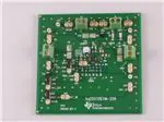
User's Guide
SLUUAA7A – July 2013 – Revised August 2014
User's Guide for bq25570 Battery Charger Evaluation
Module for Energy Harvesting
This user’s guide describes the bq25570 evaluation module (EVM), how to perform a stand-alone
evaluation and how to allow the EVM to interface with the system and host. The boost charger output is
configured to deliver up to 4.2-V maximum voltage to its output, VSTOR, using external resistors. This
voltage will be applied to the storage element as long as the storage element voltage at VBAT is above
the internally programmed undervoltage of 2.0 V. The integrated buck converter provides up to 1.8 V and
100 mA at VOUT. The VBAT_OK indicator toggles high when VSTOR ramps up to 3.0 V and toggles low
when VSTOR ramps down to 2.8 V.
1
2
3
4
5
Contents
Introduction ................................................................................................................... 2
1.1
EVM Features ....................................................................................................... 2
1.2
General Description ................................................................................................ 2
1.3
Design and Evaluation Considerations .......................................................................... 3
1.4
EVM Schematic ..................................................................................................... 4
1.5
EVM I/O Connections .............................................................................................. 5
EVM Performance Specification Summary ............................................................................... 7
Test and Measurment Summary........................................................................................... 7
3.1
Test Setups and Results ........................................................................................... 8
Bill of Materials and Board Layout ....................................................................................... 17
4.1
Bill of Materials .................................................................................................... 17
4.2
EVM Board Layout ................................................................................................ 18
PCB Layout Guideline ..................................................................................................... 20
List of Figures
1
EVM Schematic .............................................................................................................. 4
2
Test Setup for Measuring Boost Charger Efficiency .................................................................... 9
3
Charger Efficiency versus Input Voltage .................................................................................. 9
4
Charger Efficiency versus Input Current ................................................................................ 10
5
Test Setup for Measuring Buck Converter Efficiency
11
6
Buck Converter Efficiency versus Output Current
11
7
8
9
10
11
12
13
14
15
.................................................................
....................................................................
Test Setup for Performing Load Transient on Buck Output ..........................................................
50-mA Load Transient on VOUT ...........................................................................................
Charger Operational Waveforms During 50-mA Load Transient ....................................................
Buck Operational Waveforms During 50-mA Load Transient ........................................................
Test Setup for Charging a Super Capacitor from Buck Output ......................................................
Charging a Super Cap from VOUT ........................................................................................
EVM PCB Top Assembly ..................................................................................................
EVM PCB Top Layer ......................................................................................................
EVM PCB Bottom Layer ...................................................................................................
12
12
13
14
15
15
18
18
19
List of Tables
1
2
................................................. 5
Bill of Materials ............................................................................................................. 17
I/O Connections and Configuration for Evaluation of bq25570 EVM
SLUUAA7A – July 2013 – Revised August 2014
Submit Documentation Feedback
User's Guide for bq25570 Battery Charger Evaluation Module for Energy
Harvesting
Copyright © 2013–2014, Texas Instruments Incorporated
1
�Introduction
1
Introduction
1.1
EVM Features
•
•
•
•
•
•
1.2
www.ti.com
Evaluation module for bq25570
Ultra-low power boost charger and buck converter with battery management for energy harvester
applications
Resistor-programmable settings for over voltage providing flexible battery management
Programmable push-pull output indicator for battery status (VBAT_OK)
Test points for key signals available for testing purpose – easy probe hook-up.
Jumpers available – easy to change settings
General Description
The bq25570 is an integrated energy harvesting Nano-Power management solution that is well suited for
meeting the special needs of ultra-low power applications. The product is specifically designed to
efficiently acquire and manage the microwatts (µW) to miliwatts (mW) of power generated from a variety of
high output impedance (HiZ) DC sources like photovoltaic (solar) or thermal electric generators; or with an
AC/DC rectifier, a piezoelectric generator. The bq25570 implements a highly efficient, pulse-frequency
modulated (PFM) boost converter/charger targeted toward products and systems, such as wireless sensor
networks (WSN) which have stringent power and operational demands. Assuming a depleted storage
element has been attached, the bq25570 DC-DC boost converter/charger that requires only microwatts of
power to begin operating in cold start mode. Once the boost converter output, VSTOR, reaches ~1.8 V
and can now power the converter, the main boost converter can now more efficiently extract power from
low voltage output harvesters such as thermoelectric generators (TEGs) or single and dual cell solar
panels. For example, assuming the HiZ input source can provide at least 5 µW typical and the load on
VSTOR (including the storage element leakage current) is less than 1 µA of leakage current, the boost
converter can be started with VIN_DC as low as 330 mV typical, and once VSTOR reaches 1.8 V, can
continue to harvest energy down to VIN_DC ≃ 120 mV. The integrated PFM buck converter is also
powered from VSTOR and, assuming enough input power is available, provides up to 100 mA from the
VOUT pin. The VOUT voltage is externally programmed to slightly less than the VSTOR voltage.
HiZ DC sources have a maximum output power point (MPP) that varies with ambient conditions. For
example, a solar panel's MPP varies with the amount of light on the panel and with temperature. The MPP
is listed by the harvesting source manufacturer as a percentage of its open circuit (OC) voltage. Therefore,
the bq25570 implements a programmable maximum power point tracking (MPPT) sampling network to
optimize the transfer of power into the device. The bq25570 periodically samples the open circuit input
voltage every 16 seconds by disabling the boost converter for 256 ms and stores the programmed MPP
ratio of the OC voltage on the external reference capacitor (C2) at VREF_SAMP. Typically solar cells are
at their MPP when loaded to ~70–80% of their OC voltage and TEGs at ~50%. While the storage element
is less than the user programmed maximum voltage (VBAT_OV), the boost charger loads the harvesting
source until VIN_DC reaches the MPP (voltage at VREF_SAMP). This results in the boost charger
regulating the input voltage of the converter until the output reaches VBAT_OV, thus transferring the
maximum amount of power currently available per ambient conditions to the output.
The battery undervoltage, VBAT_UV, threshold is checked continuously to ensure that the internal battery
FET, connecting VSTOR to VBAT, does not turn on until VSTOR is above the VBAT_UV threshold (2.0
V).The over voltage (VBAT_OV) setting initially is lower than the programmed value at startup (varies on
conditions) and is updated after the first ~32 ms. Subsequent updates are every ~64 ms. The VBAT_OV
threshold sets maximum voltage on VSTOR and the boost converter stops switching when the voltage on
VSTOR reaches the VBAT_OV threshold. The open circuit input voltage (VIN_OC) is measured every ~16
seconds in order for the Maximum Power Point Tracking (MPPT) circuit to sample and hold the input
regulation voltage. This periodic update continually optimizes maximum power delivery based on the
harvesting conditions.
2
User's Guide for bq25570 Battery Charger Evaluation Module for Energy
Harvesting
SLUUAA7A – July 2013 – Revised August 2014
Submit Documentation Feedback
Copyright © 2013–2014, Texas Instruments Incorporated
�Introduction
www.ti.com
The bq25570 was designed with the flexibility to support a variety of energy storage elements. The
availability of the sources from which harvesters extract their energy can often be sporadic or timevarying. Systems will typically need some type of energy storage element, such as a re-chargeable
battery, super capacitor, or conventional capacitor. The storage element will make certain constant power
is available when needed for the systems. In general, the storage element also allows the system to
handle any peak currents that can not directly come from the input source. It is important to remember
that batteries and super capacitors can have significant leakage currents that need to be included with
determining the loading on VSTOR.
To prevent damage to a customer’s storage element, both maximum and minimum voltages are monitored
against the internally programmed under-voltage (VBAT_UV) and user programmed over-voltage
(VBAT_OV) levels.
To further assist users in the strict management of their energy budgets, the bq25570 toggles a user
programmable battery good flag (VBAT_OK), checked every 64 ms, to signal the microprocessor when
the voltage on an energy storage element or capacitor has risen above (OK_HYST threshold) or dropped
below (OK_PROG threshold) a pre-set critical level. To prevent the system from entering an undervoltage
condition or if starting up into a depleted storage element, it is highly recommended to isolate the system
load from VSTOR by 1) setting VBAT_OK equal to the buck converter's enable signal VOUT_EN and 2)
using an NFET to invert the BAT_OK signal so that it drives the gate of PFET, which isolates the system
load from VSTOR.
For details, see the bq25570 data sheet (SLUSBH2).
1.3
Design and Evaluation Considerations
This user's guide is not a replacement for the data sheet. Reading the data sheet first will help in
understanding the operations and features of this IC. In this document, “battery” or "VBAT" will be used
but one could substitute any appropriate storage element.
System Design Tips
Compared to designing systems powered from an AC/DC converter or large battery (for example, low
impedance sources), designing systems powered by HiZ sources requires that the system load-per-unit
time (for example, per day for solar panel) be compared to the expected loading per the same time unit.
Often there is not enough real time input harvested power (for example, at night for a solar panel) to run
the system in full operation. Therefore, the energy harvesting circuit collects more energy than being
drawn by the system when ambient conditions allow and stores that energy in a storage element for later
use to power the system. See SLUC461 for an example spreadsheet on how to design a real solar-panelpowered system in three easy steps:
1. Referring the system rail power back to VSTOR
2. Referring the required VSTOR power back to bq255xx input power
3. Computing the minimum solar panel area from the input power requirement
As demonstrated in the spreadsheet, for any boost converter, you must perform a power balance, POUT /
PIN = (VSTOR × ISTOR) / (VIN × IIN)= η where η is the estimated efficiency for the same or very similar
configuration in order to determine the minimum input power needed to supply the desired output power.
This IC is a highly efficient charger for a storage element such as a battery or super capacitor. The main
difference between a battery and a super capacitor is the capacity curve. The battery typically has little or
no capacity below a certain voltage, where as the capacitor does have capacity at lower voltages. Both
can have significant leakage currents that will appear as a DC load on VSTOR/VBAT.
SLUUAA7A – July 2013 – Revised August 2014
Submit Documentation Feedback
User's Guide for bq25570 Battery Charger Evaluation Module for Energy
Harvesting
Copyright © 2013–2014, Texas Instruments Incorporated
3
�Introduction
1.4
www.ti.com
EVM Schematic
Figure 1 is the schematic for this EVM.
VSTOR
VSTOR
TP4
VIN1
VSTOR
4.99M
JP1
VOC_SAMP
R4
10M
J1
4.99M
0.1V-4.0V
VIN J2
L1
GND
C4
4.7uF
0.1uF
VSTOR
C10
+
GND
J5
GND
VBAT
TP5
J6
J7
JP4 80%
JP1 to R3-R5
50%
R5
C5
VBAT
VOC_SAMP
VIN
TP6
C6
TP3
LBOOST TP2
LBUCK
1.8V (Adj. 1.3V-5.05V), 50mA
L2
J11
5
EN
17
18
19
16
LBUCK
NC
VBAT
VSTOR
22uF
6
VSS
15
VOUT
14
VBAT_OK
13
VOUT_SET
12
OK_PROG
11
C9
1
TP8
VOUT
J9
GND
GND
J12
GND
OK_HYST
VREF_SAMP
+
C3
J13
BAT_OK
10
VOC_SAMP
4
NC
3
9
4.7uF
0.1uF
TP9
VRDIV
C7
BQ25570RGR
BQ25570RGR
VBAT_OV
VOC_SAMP
C1
VIN_DC
VOUT_EN
1
C8
VSS
2
8
+
1
7
VIN1
20
21
PWPD
TP1
LBOOST
U1
GND
J8
VOUT
10 uH
J3
4.2V (Adj. up to 5.25V)
VBAT
J10
100u
22uH
GND
4.2V (Adj. up to 5.25V), 100mA
J4
1
R3
GND
VRDIV
VRDIV
BAT_OK
R6
VREF_SAMP
GND
TP7
JP5
JP6
887k
VOUT_EN
VRDIV
C2
0.01uF
R1
7.5M
R7
6.98M
R2
5.76M
R8
5.36M
R9
4.22M
VBAT
VBAT
/EN
GND
R10
8.66M
JP2
VSTOR
VSTOR
VOUT_EN
GND
JP3
1
Not Installed
Figure 1. EVM Schematic
4
User's Guide for bq25570 Battery Charger Evaluation Module for Energy
Harvesting
Copyright © 2013–2014, Texas Instruments Incorporated
SLUUAA7A – July 2013 – Revised August 2014
Submit Documentation Feedback
�Introduction
www.ti.com
1.5
EVM I/O Connections
Table 1. I/O Connections and Configuration for Evaluation of bq25570 EVM
Headers and
Terminals
Description
Comments/Recommended Setting
J1–VIN
Input source (+)
J2 - VIN/GND
Input source terminal block
J3–GND
Input source return (–)
If VIN_DC is higher than VSTOR and VSTOR is equal to VBAT_OV, the input VIN_DC is pulled to ground
through a small resistance to stop further charging of the attached battery or capacitor. It is critical that if
this case is expected, the impedance of the source attached to VIN_DC be higher than 20 Ω and not a
low impedance source.
J4 - VSTOR
Boost charger output (+)
Buck converter input
J5 - VSTOR/GND
Boost charger output terminal block
J6 - GND
Boost charger return (-)
J7– VBAT
Rechargeable storage element connection (+)
J8 - VBAT/GND
Rechargeable storage element terminal block
J9–GND
Rechargeable storage element connection return (–)
J10 – VOUT
Buck converter output (+)
J11 - VOUT/GND
Buck converter output terminal block
J12 -GND
Buck converter output (-)
J13 – BAT_OK
Battery Status Indicator (+/-)
Test Points
TP1
Input source (+)
TP2
Boost charger switching node
TP3
Buck converter switching node
TP4
Boost charger output, VSTOR (+)
TP5
Rechargeable storage element connection, BAT_SEC (+)
TP6
Buck converter output, VOUT (+)
TP7
VRDIV node
TP8
Output return (-)
TP9
Input return (-)
CAUTION Providing an additional low impedance current path in parallel with the feedback resistors , for
example, with a 10 MΩ scope probe attached, will degrade regulation accuracy.
Jumpers
JP1 – VOC_SAMP
VOC_SAMP = external resistors sized to configure the IC Uninstalled (NOTE: Do not install if JP4 shunt is installed)
to regulate VIN to 75% of VOC_SAMP.
JP2 - /EN
/EN = GND enables the IC. /EN=VSTOR disables the IC.
/EN=GND
JP3 - VOUT_EN
VOUT_EN = VSTOR enables the buck converter when
VSTOR is up VOUT_EN = GND disables the buck
converter
VOUT_EN=VSTOR (NOTE: Do not install if JP6 shunt is installed)
SLUUAA7A – July 2013 – Revised August 2014
Submit Documentation Feedback
User's Guide for bq25570 Battery Charger Evaluation Module for Energy
Harvesting
Copyright © 2013–2014, Texas Instruments Incorporated
5
�Introduction
www.ti.com
Table 1. I/O Connections and Configuration for Evaluation of bq25570 EVM (continued)
Headers and
Terminals
Description
Comments/Recommended Setting
JP4 - VOC_SAMP
VOC_SAMP = 80% configures the IC to regulate VIN to
80% of OCV. VOC_SAMP = 50% configures the IC to
regulate VIN to 50% of OCV.
JP4 = 80% (NOTE: Do not install if JP1 shunt is installed)
JP5 - VREF_SAMP to
GND
VREF_SAMP = GND
Uninstalled (NOTE: Providing an additional leakage path for the VREF_SAMP capacitor for example,
through a 10 MΩ scope probe attached to VREF_SAMP, will degrade input voltage regulation
performance).
JP6 - VBAT_OK to
VOUT_EN
BAT_OK=VOUT_EN configures the buck converter to be
enabled only when VSTOR is greater than the VBAT_OK
threshold per the resistors (2.786V on the EVM)
Uninstalled (NOTE: Do not install if JP3 shunt is installed)
6
User's Guide for bq25570 Battery Charger Evaluation Module for Energy
Harvesting
Copyright © 2013–2014, Texas Instruments Incorporated
SLUUAA7A – July 2013 – Revised August 2014
Submit Documentation Feedback
�EVM Performance Specification Summary
www.ti.com
2
EVM Performance Specification Summary
See Data Sheet “Recommended Operating Conditions” for component adjustments. For details about the
resistor programmable settings, see bq25570 data sheet (SLUSBH2).
MIN
NOM
UNIT
VIN(DC)
DC input voltage into VIN_DC
VIN_Start-up(DC)
DC minimum start-up voltage into depleted storage element, no load attached
to VSTOR or VOUT and IBATLEAK 1MΩ is
recommended. However, during board assembly, contaminants such as solder flux and even some board
cleaning agents can leave residue that may form parasitic resistors across the physical resistors and/or
from one end of a resistor to ground, especially in humid, fast airflow environments. This can result in the
voltage regulation and threshold levels changing significantly from those expected per the installed resistor
values. Therefore, it is highly recommended that no ground planes be poured near the voltage setting
resistors. In addition, the boards must be carefully cleaned, possibly rotated at least once during cleaning,
and then rinsed with de-ionized water until the ionic contamination of that water is well above 50 MOhm. If
this is not feasible, then it is recommended that the sum of the voltage setting resistors be reduced to at
least 5X below the measured ionic contamination.
Revision History
Changes from Original (July 2013) to A Revision ........................................................................................................... Page
•
Changed contents in the bill of materials ............................................................................................. 17
NOTE: Page numbers for previous revisions may differ from page numbers in the current version.
20
Revision History
SLUUAA7A – July 2013 – Revised August 2014
Submit Documentation Feedback
Copyright © 2013–2014, Texas Instruments Incorporated
�ADDITIONAL TERMS AND CONDITIONS, WARNINGS, RESTRICTIONS, AND DISCLAIMERS FOR
EVALUATION MODULES
Texas Instruments Incorporated (TI) markets, sells, and loans all evaluation boards, kits, and/or modules (EVMs) pursuant to, and user
expressly acknowledges, represents, and agrees, and takes sole responsibility and risk with respect to, the following:
1.
User agrees and acknowledges that EVMs are intended to be handled and used for feasibility evaluation only in laboratory and/or
development environments. Notwithstanding the foregoing, in certain instances, TI makes certain EVMs available to users that do not
handle and use EVMs solely for feasibility evaluation only in laboratory and/or development environments, but may use EVMs in a
hobbyist environment. All EVMs made available to hobbyist users are FCC certified, as applicable. Hobbyist users acknowledge, agree,
and shall comply with all applicable terms, conditions, warnings, and restrictions in this document and are subject to the disclaimer and
indemnity provisions included in this document.
2. Unless otherwise indicated, EVMs are not finished products and not intended for consumer use. EVMs are intended solely for use by
technically qualified electronics experts who are familiar with the dangers and application risks associated with handling electrical
mechanical components, systems, and subsystems.
3. User agrees that EVMs shall not be used as, or incorporated into, all or any part of a finished product.
4. User agrees and acknowledges that certain EVMs may not be designed or manufactured by TI.
5. User must read the user's guide and all other documentation accompanying EVMs, including without limitation any warning or
restriction notices, prior to handling and/or using EVMs. Such notices contain important safety information related to, for example,
temperatures and voltages. For additional information on TI's environmental and/or safety programs, please visit www.ti.com/esh or
contact TI.
6. User assumes all responsibility, obligation, and any corresponding liability for proper and safe handling and use of EVMs.
7. Should any EVM not meet the specifications indicated in the user’s guide or other documentation accompanying such EVM, the EVM
may be returned to TI within 30 days from the date of delivery for a full refund. THE FOREGOING LIMITED WARRANTY IS THE
EXCLUSIVE WARRANTY MADE BY TI TO USER AND IS IN LIEU OF ALL OTHER WARRANTIES, EXPRESSED, IMPLIED, OR
STATUTORY, INCLUDING ANY WARRANTY OF MERCHANTABILITY OR FITNESS FOR ANY PARTICULAR PURPOSE. TI SHALL
NOT BE LIABLE TO USER FOR ANY INDIRECT, SPECIAL, INCIDENTAL, OR CONSEQUENTIAL DAMAGES RELATED TO THE
HANDLING OR USE OF ANY EVM.
8. No license is granted under any patent right or other intellectual property right of TI covering or relating to any machine, process, or
combination in which EVMs might be or are used. TI currently deals with a variety of customers, and therefore TI’s arrangement with
the user is not exclusive. TI assumes no liability for applications assistance, customer product design, software performance, or
infringement of patents or services with respect to the handling or use of EVMs.
9. User assumes sole responsibility to determine whether EVMs may be subject to any applicable federal, state, or local laws and
regulatory requirements (including but not limited to U.S. Food and Drug Administration regulations, if applicable) related to its handling
and use of EVMs and, if applicable, compliance in all respects with such laws and regulations.
10. User has sole responsibility to ensure the safety of any activities to be conducted by it and its employees, affiliates, contractors or
designees, with respect to handling and using EVMs. Further, user is responsible to ensure that any interfaces (electronic and/or
mechanical) between EVMs and any human body are designed with suitable isolation and means to safely limit accessible leakage
currents to minimize the risk of electrical shock hazard.
11. User shall employ reasonable safeguards to ensure that user’s use of EVMs will not result in any property damage, injury or death,
even if EVMs should fail to perform as described or expected.
12. User shall be solely responsible for proper disposal and recycling of EVMs consistent with all applicable federal, state, and local
requirements.
Certain Instructions. User shall operate EVMs within TI’s recommended specifications and environmental considerations per the user’s
guide, accompanying documentation, and any other applicable requirements. Exceeding the specified ratings (including but not limited to
input and output voltage, current, power, and environmental ranges) for EVMs may cause property damage, personal injury or death. If
there are questions concerning these ratings, user should contact a TI field representative prior to connecting interface electronics including
input power and intended loads. Any loads applied outside of the specified output range may result in unintended and/or inaccurate
operation and/or possible permanent damage to the EVM and/or interface electronics. Please consult the applicable EVM user's guide prior
to connecting any load to the EVM output. If there is uncertainty as to the load specification, please contact a TI field representative. During
normal operation, some circuit components may have case temperatures greater than 60°C as long as the input and output are maintained
at a normal ambient operating temperature. These components include but are not limited to linear regulators, switching transistors, pass
transistors, and current sense resistors which can be identified using EVMs’ schematics located in the applicable EVM user's guide. When
placing measurement probes near EVMs during normal operation, please be aware that EVMs may become very warm. As with all
electronic evaluation tools, only qualified personnel knowledgeable in electronic measurement and diagnostics normally found in
development environments should use EVMs.
Agreement to Defend, Indemnify and Hold Harmless. User agrees to defend, indemnify, and hold TI, its directors, officers, employees,
agents, representatives, affiliates, licensors and their representatives harmless from and against any and all claims, damages, losses,
expenses, costs and liabilities (collectively, "Claims") arising out of, or in connection with, any handling and/or use of EVMs. User’s
indemnity shall apply whether Claims arise under law of tort or contract or any other legal theory, and even if EVMs fail to perform as
described or expected.
Safety-Critical or Life-Critical Applications. If user intends to use EVMs in evaluations of safety critical applications (such as life support),
and a failure of a TI product considered for purchase by user for use in user’s product would reasonably be expected to cause severe
personal injury or death such as devices which are classified as FDA Class III or similar classification, then user must specifically notify TI
of such intent and enter into a separate Assurance and Indemnity Agreement.
�RADIO FREQUENCY REGULATORY COMPLIANCE INFORMATION FOR EVALUATION MODULES
Texas Instruments Incorporated (TI) evaluation boards, kits, and/or modules (EVMs) and/or accompanying hardware that is marketed, sold,
or loaned to users may or may not be subject to radio frequency regulations in specific countries.
General Statement for EVMs Not Including a Radio
For EVMs not including a radio and not subject to the U.S. Federal Communications Commission (FCC) or Industry Canada (IC)
regulations, TI intends EVMs to be used only for engineering development, demonstration, or evaluation purposes. EVMs are not finished
products typically fit for general consumer use. EVMs may nonetheless generate, use, or radiate radio frequency energy, but have not been
tested for compliance with the limits of computing devices pursuant to part 15 of FCC or the ICES-003 rules. Operation of such EVMs may
cause interference with radio communications, in which case the user at his own expense will be required to take whatever measures may
be required to correct this interference.
General Statement for EVMs including a radio
User Power/Frequency Use Obligations: For EVMs including a radio, the radio included in such EVMs is intended for development and/or
professional use only in legally allocated frequency and power limits. Any use of radio frequencies and/or power availability in such EVMs
and their development application(s) must comply with local laws governing radio spectrum allocation and power limits for such EVMs. It is
the user’s sole responsibility to only operate this radio in legally acceptable frequency space and within legally mandated power limitations.
Any exceptions to this are strictly prohibited and unauthorized by TI unless user has obtained appropriate experimental and/or development
licenses from local regulatory authorities, which is the sole responsibility of the user, including its acceptable authorization.
U.S. Federal Communications Commission Compliance
For EVMs Annotated as FCC – FEDERAL COMMUNICATIONS COMMISSION Part 15 Compliant
Caution
This device complies with part 15 of the FCC Rules. Operation is subject to the following two conditions: (1) This device may not cause
harmful interference, and (2) this device must accept any interference received, including interference that may cause undesired operation.
Changes or modifications could void the user's authority to operate the equipment.
FCC Interference Statement for Class A EVM devices
This equipment has been tested and found to comply with the limits for a Class A digital device, pursuant to part 15 of the FCC Rules.
These limits are designed to provide reasonable protection against harmful interference when the equipment is operated in a commercial
environment. This equipment generates, uses, and can radiate radio frequency energy and, if not installed and used in accordance with the
instruction manual, may cause harmful interference to radio communications. Operation of this equipment in a residential area is likely to
cause harmful interference in which case the user will be required to correct the interference at its own expense.
FCC Interference Statement for Class B EVM devices
This equipment has been tested and found to comply with the limits for a Class B digital device, pursuant to part 15 of the FCC Rules.
These limits are designed to provide reasonable protection against harmful interference in a residential installation. This equipment
generates, uses and can radiate radio frequency energy and, if not installed and used in accordance with the instructions, may cause
harmful interference to radio communications. However, there is no guarantee that interference will not occur in a particular installation. If
this equipment does cause harmful interference to radio or television reception, which can be determined by turning the equipment off and
on, the user is encouraged to try to correct the interference by one or more of the following measures:
• Reorient or relocate the receiving antenna.
• Increase the separation between the equipment and receiver.
• Connect the equipment into an outlet on a circuit different from that to which the receiver is connected.
• Consult the dealer or an experienced radio/TV technician for help.
Industry Canada Compliance (English)
For EVMs Annotated as IC – INDUSTRY CANADA Compliant:
This Class A or B digital apparatus complies with Canadian ICES-003.
Changes or modifications not expressly approved by the party responsible for compliance could void the user’s authority to operate the
equipment.
Concerning EVMs Including Radio Transmitters
This device complies with Industry Canada licence-exempt RSS standard(s). Operation is subject to the following two conditions: (1) this
device may not cause interference, and (2) this device must accept any interference, including interference that may cause undesired
operation of the device.
Concerning EVMs Including Detachable Antennas
Under Industry Canada regulations, this radio transmitter may only operate using an antenna of a type and maximum (or lesser) gain
approved for the transmitter by Industry Canada. To reduce potential radio interference to other users, the antenna type and its gain should
be so chosen that the equivalent isotropically radiated power (e.i.r.p.) is not more than that necessary for successful communication.
This radio transmitter has been approved by Industry Canada to operate with the antenna types listed in the user guide with the maximum
permissible gain and required antenna impedance for each antenna type indicated. Antenna types not included in this list, having a gain
greater than the maximum gain indicated for that type, are strictly prohibited for use with this device.
�Canada Industry Canada Compliance (French)
Cet appareil numérique de la classe A ou B est conforme à la norme NMB-003 du Canada
Les changements ou les modifications pas expressément approuvés par la partie responsable de la conformité ont pu vider l’autorité de
l'utilisateur pour actionner l'équipement.
Concernant les EVMs avec appareils radio
Le présent appareil est conforme aux CNR d'Industrie Canada applicables aux appareils radio exempts de licence. L'exploitation est
autorisée aux deux conditions suivantes : (1) l'appareil ne doit pas produire de brouillage, et (2) l'utilisateur de l'appareil doit accepter tout
brouillage radioélectrique subi, même si le brouillage est susceptible d'en compromettre le fonctionnement.
Concernant les EVMs avec antennes détachables
Conformément à la réglementation d'Industrie Canada, le présent émetteur radio peut fonctionner avec une antenne d'un type et d'un gain
maximal (ou inférieur) approuvé pour l'émetteur par Industrie Canada. Dans le but de réduire les risques de brouillage radioélectrique à
l'intention des autres utilisateurs, il faut choisir le type d'antenne et son gain de sorte que la puissance isotrope rayonnée équivalente
(p.i.r.e.) ne dépasse pas l'intensité nécessaire à l'établissement d'une communication satisfaisante.
Le présent émetteur radio a été approuvé par Industrie Canada pour fonctionner avec les types d'antenne énumérés dans le manuel
d’usage et ayant un gain admissible maximal et l'impédance requise pour chaque type d'antenne. Les types d'antenne non inclus dans
cette liste, ou dont le gain est supérieur au gain maximal indiqué, sont strictement interdits pour l'exploitation de l'émetteur.
Mailing Address: Texas Instruments, Post Office Box 655303, Dallas, Texas 75265
Copyright © 2014, Texas Instruments Incorporated
spacer
Important Notice for Users of EVMs Considered “Radio Frequency Products” in Japan
EVMs entering Japan are NOT certified by TI as conforming to Technical Regulations of Radio Law of Japan.
If user uses EVMs in Japan, user is required by Radio Law of Japan to follow the instructions below with respect to EVMs:
1.
2.
3.
Use EVMs in a shielded room or any other test facility as defined in the notification #173 issued by Ministry of Internal Affairs and
Communications on March 28, 2006, based on Sub-section 1.1 of Article 6 of the Ministry’s Rule for Enforcement of Radio Law of
Japan,
Use EVMs only after user obtains the license of Test Radio Station as provided in Radio Law of Japan with respect to EVMs, or
Use of EVMs only after user obtains the Technical Regulations Conformity Certification as provided in Radio Law of Japan with respect
to EVMs. Also, do not transfer EVMs, unless user gives the same notice above to the transferee. Please note that if user does not
follow the instructions above, user will be subject to penalties of Radio Law of Japan.
http://www.tij.co.jp
【無線電波を送信する製品の開発キットをお使いになる際の注意事項】 本開発キットは技術基準適合証明を受けておりません。 本製品の
ご使用に際しては、電波法遵守のため、以下のいずれかの措置を取っていただく必要がありますのでご注意ください。
1.
2.
3.
電波法施行規則第6条第1項第1号に基づく平成18年3月28日総務省告示第173号で定められた電波暗室等の試験設備でご使用いただく。
実験局の免許を取得後ご使用いただく。
技術基準適合証明を取得後ご使用いただく。。
なお、本製品は、上記の「ご使用にあたっての注意」を譲渡先、移転先に通知しない限り、譲渡、移転できないものとします
上記を遵守頂けない場合は、電波法の罰則が適用される可能性があることをご留意ください。
日本テキサス・インスツルメンツ株式会社
東京都新宿区西新宿6丁目24番1号
西新宿三井ビル
http://www.tij.co.jp
Texas Instruments Japan Limited
(address) 24-1, Nishi-Shinjuku 6 chome, Shinjuku-ku, Tokyo, Japan
�IMPORTANT NOTICE
Texas Instruments Incorporated and its subsidiaries (TI) reserve the right to make corrections, enhancements, improvements and other
changes to its semiconductor products and services per JESD46, latest issue, and to discontinue any product or service per JESD48, latest
issue. Buyers should obtain the latest relevant information before placing orders and should verify that such information is current and
complete. All semiconductor products (also referred to herein as “components”) are sold subject to TI’s terms and conditions of sale
supplied at the time of order acknowledgment.
TI warrants performance of its components to the specifications applicable at the time of sale, in accordance with the warranty in TI’s terms
and conditions of sale of semiconductor products. Testing and other quality control techniques are used to the extent TI deems necessary
to support this warranty. Except where mandated by applicable law, testing of all parameters of each component is not necessarily
performed.
TI assumes no liability for applications assistance or the design of Buyers’ products. Buyers are responsible for their products and
applications using TI components. To minimize the risks associated with Buyers’ products and applications, Buyers should provide
adequate design and operating safeguards.
TI does not warrant or represent that any license, either express or implied, is granted under any patent right, copyright, mask work right, or
other intellectual property right relating to any combination, machine, or process in which TI components or services are used. Information
published by TI regarding third-party products or services does not constitute a license to use such products or services or a warranty or
endorsement thereof. Use of such information may require a license from a third party under the patents or other intellectual property of the
third party, or a license from TI under the patents or other intellectual property of TI.
Reproduction of significant portions of TI information in TI data books or data sheets is permissible only if reproduction is without alteration
and is accompanied by all associated warranties, conditions, limitations, and notices. TI is not responsible or liable for such altered
documentation. Information of third parties may be subject to additional restrictions.
Resale of TI components or services with statements different from or beyond the parameters stated by TI for that component or service
voids all express and any implied warranties for the associated TI component or service and is an unfair and deceptive business practice.
TI is not responsible or liable for any such statements.
Buyer acknowledges and agrees that it is solely responsible for compliance with all legal, regulatory and safety-related requirements
concerning its products, and any use of TI components in its applications, notwithstanding any applications-related information or support
that may be provided by TI. Buyer represents and agrees that it has all the necessary expertise to create and implement safeguards which
anticipate dangerous consequences of failures, monitor failures and their consequences, lessen the likelihood of failures that might cause
harm and take appropriate remedial actions. Buyer will fully indemnify TI and its representatives against any damages arising out of the use
of any TI components in safety-critical applications.
In some cases, TI components may be promoted specifically to facilitate safety-related applications. With such components, TI’s goal is to
help enable customers to design and create their own end-product solutions that meet applicable functional safety standards and
requirements. Nonetheless, such components are subject to these terms.
No TI components are authorized for use in FDA Class III (or similar life-critical medical equipment) unless authorized officers of the parties
have executed a special agreement specifically governing such use.
Only those TI components which TI has specifically designated as military grade or “enhanced plastic” are designed and intended for use in
military/aerospace applications or environments. Buyer acknowledges and agrees that any military or aerospace use of TI components
which have not been so designated is solely at the Buyer's risk, and that Buyer is solely responsible for compliance with all legal and
regulatory requirements in connection with such use.
TI has specifically designated certain components as meeting ISO/TS16949 requirements, mainly for automotive use. In any case of use of
non-designated products, TI will not be responsible for any failure to meet ISO/TS16949.
Products
Applications
Audio
www.ti.com/audio
Automotive and Transportation
www.ti.com/automotive
Amplifiers
amplifier.ti.com
Communications and Telecom
www.ti.com/communications
Data Converters
dataconverter.ti.com
Computers and Peripherals
www.ti.com/computers
DLP® Products
www.dlp.com
Consumer Electronics
www.ti.com/consumer-apps
DSP
dsp.ti.com
Energy and Lighting
www.ti.com/energy
Clocks and Timers
www.ti.com/clocks
Industrial
www.ti.com/industrial
Interface
interface.ti.com
Medical
www.ti.com/medical
Logic
logic.ti.com
Security
www.ti.com/security
Power Mgmt
power.ti.com
Space, Avionics and Defense
www.ti.com/space-avionics-defense
Microcontrollers
microcontroller.ti.com
Video and Imaging
www.ti.com/video
RFID
www.ti-rfid.com
OMAP Applications Processors
www.ti.com/omap
TI E2E Community
e2e.ti.com
Wireless Connectivity
www.ti.com/wirelessconnectivity
Mailing Address: Texas Instruments, Post Office Box 655303, Dallas, Texas 75265
Copyright © 2014, Texas Instruments Incorporated
�