Product
Folder
Order
Now
Support &
Community
Tools &
Software
Technical
Documents
BQ25887
SLUSD89B – FEBRUARY 2019 – REVISED NOVEMBER 2019
BQ25887 I2C Controlled 2-Cell, 2-A Boost-Mode Battery Charger With Cell Balancing For
USB Input
1 Features
•
1
•
•
•
•
•
High-efficiency 2-A, 1.5-MHz switch mode boost
charger
– 93.4% Charge efficiency at 5-V adapter, 7.6-V
battery, 1-A charge
– Optimized for USB input and 2-cell Li-Ion
battery
– Selectable low power PFM mode for light load
operation
Single input to support USB input adapters
– Supports 3.9-V to 6.2-V input voltage range
with 20-V absolute maximum input voltage
rating
– Input current limit (500 mA to 3.3 A with 100mA resolution) to support USB2.0, USB3.0
standard adapters
– Maximum power tracking by input voltage limit
up-to 5.5 V
Cell balancing and I2C control
– Integrated FETs for balancing current up to
400 mA
– Automatic cell balancing with default register
setting
Input current optimizer (ICO) to maximize input
power without overloading adapters
Integrated 16-bit ADC for system monitoring (BUS
voltage and current, each cell voltage, charge
current, and NTC and die temperature)
High integration includes all MOSFETs, current
sensing and loop compensation
•
•
High accuracy
– ±0.5% Charge voltage regulation
– ±5% Charge current regulation
– ±7.5% Input current regulation
Safety
– Battery temperature sensing in charge
– Thermal regulation and thermal shutdown
2 Applications
•
•
•
•
Electronic and robotic toys
Virtual reality headset
IP network camera
Drone payload control
3 Description
The BQ25887 is a highly-integrated 2-A boost switchmode battery charge management device for 2-cell
(2s) Li-Ion and Li-polymer battery. The BQ25887 has
I2C control with cell balancing for USB input.
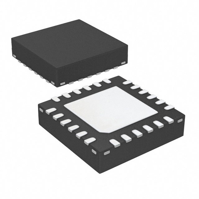
Device Information(1)
PART NUMBER
BQ25887
PACKAGE
BODY SIZE (NOM)
VQFN (24)
4.00 mm x 4.00 mm
(1) For all available packages, see the orderable addendum at
the end of the data sheet.
Simplified Schematic
5V @ 3A
VREF
VBUS
STAT
PMID
ILIM
SW
SNS
BTST
BAT
ICHG=2A
REGN
VREF
SDA
CBSET
REGN
SCL
Host
/INT
2s Battery
MID
TS
/PG
CD
PSEL
`
BQ25887
GND
1
An IMPORTANT NOTICE at the end of this data sheet addresses availability, warranty, changes, use in safety-critical applications,
intellectual property matters and other important disclaimers. PRODUCTION DATA.
�BQ25887
SLUSD89B – FEBRUARY 2019 – REVISED NOVEMBER 2019
www.ti.com
Table of Contents
1
2
3
4
5
6
7
Features ..................................................................
Applications ...........................................................
Description .............................................................
Revision History.....................................................
Device Comparison Table.....................................
Pin Configuration and Functions .........................
Specifications.........................................................
7.1
7.2
7.3
7.4
7.5
7.6
7.7
8
1
1
1
2
3
4
6
Absolute Maximum Ratings ...................................... 6
ESD Ratings.............................................................. 6
Recommended Operating Conditions....................... 6
Thermal Information .................................................. 7
Electrical Characteristics........................................... 7
Timing Requirements .............................................. 11
Typical Characteristics ............................................ 13
Detailed Description ............................................ 15
8.1 Overview ................................................................. 15
8.2 Functional Block Diagram ....................................... 15
8.3 Feature Description................................................. 16
8.4 Device Functional Modes........................................ 30
8.5 Register Maps ........................................................ 31
9
Application and Implementation ........................ 69
9.1 Application Information............................................ 69
9.2 Typical Application .................................................. 69
10 Power Supply Recommendations ..................... 74
11 Layout................................................................... 74
11.1 Layout Guidelines ................................................. 74
11.2 Layout Example .................................................... 75
12 Device and Documentation Support ................. 76
12.1
12.2
12.3
12.4
12.5
12.6
12.7
Device Support ....................................................
Documentation Support ........................................
Receiving Notification of Documentation Updates
Support Resources ...............................................
Trademarks ...........................................................
Electrostatic Discharge Caution ............................
Glossary ................................................................
76
76
76
76
76
76
76
13 Mechanical, Packaging, and Orderable
Information ........................................................... 77
4 Revision History
NOTE: Page numbers for previous revisions may differ from page numbers in the current version.
Changes from Revision A (May 2019) to Revision B
Page
•
Changed Applications section ................................................................................................................................................ 1
•
Deleted no OTG and no power path from Description .......................................................................................................... 1
•
Added note to Absolute Maximum Ratings ........................................................................................................................... 7
•
Added Figure 79 .................................................................................................................................................................. 72
•
Added Figure 80 ................................................................................................................................................................... 72
Changes from Original (February 2019) to Revision A
•
2
Page
Changed from Advance Information to Production Data........................................................................................................ 1
Submit Documentation Feedback
Copyright © 2019, Texas Instruments Incorporated
�BQ25887
www.ti.com
SLUSD89B – FEBRUARY 2019 – REVISED NOVEMBER 2019
5 Device Comparison Table
PART NUMBER
BQ25882
BQ25883
BQ25886
BQ25887
VBUS Operating Range
3.9 to 6.2 V
3.9 to 6.2 V
4.3 to 6.2 V
3.9 to 6.2 V
USB Detection
D+/D-
D+/D-
D+/D-
PSEL
Power path
Yes
Yes
Yes
No
Cell Balancing
No
No
No
Yes
OTG
Up to 2 A
Up to 2 A
Up to 2 A
No OTG
16 bit ADC
Yes
Yes
No
Yes
Control Interface
I2C
I2C
Standalone
I2C
Status Pin
/PG
STAT, /PG
STAT, /PG
STAT, /PG
Package
2.1x2.1 WCSP-25
4x4 QFN-24
4x4 QFN-24
4x4 QFN-24
Copyright © 2019, Texas Instruments Incorporated
Submit Documentation Feedback
3
�BQ25887
SLUSD89B – FEBRUARY 2019 – REVISED NOVEMBER 2019
www.ti.com
6 Pin Configuration and Functions
RGE Package
24-Pin VQFN
Top View
PSEL
VBUS
PMID
PMID
GND
GND
24
23
22
21
20
19
PG
1
18
SW
STAT
2
17
SW
CD
3
16
SNS
SDA
4
15
SNS
SCL
5
14
BAT
INT
6
13
BAT
BQ25887
RGE, 4x4
8
9
10
11
TS
ILIM
MID
CBSET
REGN
12
BTST
7
Pin Functions
PIN
NAME
NO.
I/O
DESCRIPTION
PG
1
DO
Open drain active low power good indicator – Connect to the pull up rail via 10-kΩ resistor. LOW
indicates a good input source if the input voltage is within VVBUS_OP, and can provide more than
IPOORSRC (30mA).
STAT
2
DO
Open drain charge status indicator – Connect to the pull-up rail via 10-kΩ resistor. LOW indicates
charge in progress. HIGH indicates charge complete or charge disabled. When any fault occurs, the
STAT pin blinks at 1Hz. The STAT function can be disabled when the STAT_DIS bit is set.
CD
3
DI
Active High Chip Disable Pin – Pull CD high to disable charge and place the device in HIZ mode.
ADC operation and I2C is still allowed when CD is high. Converter is enabled when CD pin is LOW
and EN_CHG bit is 1. CD pin is internally pulled low with 900-kΩ resistor.
SDA
4
DIO
I2C Interface Data – Connect SDA to the pull up rail through a 10-kΩ resistor.
SCL
5
DI
I2C Interface Clock – Connect SCL to the pull up rail through a 10-kΩ resistor.
INT
6
DO
Open drain active Interrupt Output – Connect INT to the pull up rail via a 10-kΩ resistor. The INT
pin sends active low, 256-µs pulse to the host to report charger device status and fault.
TS
7
AI
Temperature Qualification Voltage – Connect a negative temperature coefficient thermistor.
Program temperature window with a resistor divider from REGN to TS to GND. Charge suspends
when TS pin is out of range. Recommend 103AT-2 thermistor.
AI
Input Current Limit (IINDPM) – ILIM pin sets the maximum input current and can be used to
monitor input current. IINDPM loop regulates ILIM pin voltage at 0.8V. When ILIM pin is less than
0.8V, the input current can be calculated by IIN = KILIM x VILIM / (RILIM x 0.8V). A resistor
connected from ILIM pin to ground sets the input current limit as maximum (IINMAX = KILIM /
RILIM). When ILIM pin is short to GND, the input current limit is set to maximum by ILIM. The actual
input current limit is the lower limit set by ILIM pin (when EN_ILIM bit is HIGH) or IINDPM register
bits. Input current limit less than 500mA is not supported on ILIM pin. The ILIM pin function can be
disabled when EN_ILIM bit is 0. If ILIM pin is not used, pull this pin to GND.Do not float this pin.
AI
Voltage Input for Mid Point Between Cells in 2S1P Configuration – Connect MID to the negative
terminal of the top cell and the positive terminal of the bottom cell. This pin measures the voltage of
the bottom cell for cell balancing and VMID ADC measurement. For protection of bottom cell reverse
plug in, connect a 300 ohm resistor in series between MID pin and mid connection point of the two
battery cell.
ILIM
MID
4
8
9
Submit Documentation Feedback
Copyright © 2019, Texas Instruments Incorporated
�BQ25887
www.ti.com
SLUSD89B – FEBRUARY 2019 – REVISED NOVEMBER 2019
Pin Functions (continued)
PIN
I/O
DESCRIPTION
NAME
NO.
CBSET
10
P
Power pin for Cell Balancing – Connect CBSET to the mid point between the two batteries in 2S
configuration with a current limit resistor. The resistor value determines the cell balancing current as
calculated in Cell Balancing Section. The resistor chosen should not exceed 400 mA for cell
balancing.
REGN
11
P
Gate Drive Supply – Bias supply for internal MOSFETs driver and IC. Bypass REGN to GND with a
4.7-µF ceramic capacitor. REGN current limit is 50 mA.
BTST
12
P
PWM High-side Driver Supply – Internally, BTST is connected to the cathode of the boot-strap
diode. Connect a 47nF bootstrap capacitor from SW to BTST.
BAT
13, 14
P
Battery Power Connection – Connect minimum recommended 10-µF capacitance after derating
closely to the BAT pin and GND.
SNS
15, 16
AO
SW
17, 18
P
Inductor Connection – Connect to the switched side of the external inductor.
GND
19, 20
–
Ground Return
PMID
21, 22
P
Blocking MOSFET Connection – The minimum recommended total input low-ESR capacitance on
VBUS and PMID, after applied derating, is 10 uF. At least 1-uF is recommended at VBUS with the
remainder at PMID. Typical value for PMID is 10 uF.
VBUS
23
P
Input Supply – VBUS is connected to the external DC supply. Bypass VBUS to GND with at least 1µF ceramic capacitor, placed as close to the IC as possible.
PSEL
24
DI
Power Source Selection – HIGH indicates USB host source (500mA) and LOW indicates adapter
source (3.0A).
Sense Output – Charge current sense pin. Place a 44-µF ceramic capacitor on this pin for stability
of this output.
Copyright © 2019, Texas Instruments Incorporated
Submit Documentation Feedback
5
�BQ25887
SLUSD89B – FEBRUARY 2019 – REVISED NOVEMBER 2019
www.ti.com
7 Specifications
7.1 Absolute Maximum Ratings
over operating free-air temperature range (unless otherwise noted)
(1)
MIN
MAX
VBUS (converter not switching)
-0.3
20
V
PMID (converter not switching)
-0.3
8.5
V
BAT, SNS, MID, CBSET (converter not switching)
-0.3
12
V
(2)
13
V
BTST
-0.3
19
V
REGN, STAT, /PG, TS
-0.3
6
V
ILIM
-0.3
5
V
BTST to SW
-0.3
6
V
SDA, SCL, /INT, CD, PSEL,
-0.3
6
V
0
12
V
6
mA
SW
Voltage Range (with respect to GND unless otherwise
specified)
-0.3
Voltage Range (with respect to GND unless otherwise
specified)
BAT to CBSET
Output Sink Current
/INT, STAT, /PG
UNIT
Junction Temperature, TJ
–40
150
°C
Storage temperature, Tstg
–40
150
°C
(1)
(2)
Stresses beyond those listed under Absolute Maximum Ratings may cause permanent damage to the device. Theseare stress ratings
only, which do not imply functional operation of the device at these or anyother conditions beyond those indicated under Recommended
OperatingConditions. Exposure to absolute-maximum-rated conditions for extended periods mayaffect device reliability.
-2V for 50ns
7.2 ESD Ratings
VALUE
V(ESD)
(1)
(2)
Electrostatic discharge
Human body model (HBM), per
ANSI/ESDA/JEDEC JS-001 (1)
±2000
Charged device model (CDM), per JEDEC
specification JESD22-C101 (2)
±250
UNIT
V
JEDEC document JEP155 states that 500-V HBM allows safe manufacturing with a standard ESD control process.
JEDEC document JEP157 states that 250-V CDM allows safe manufacturing with a standard ESD control process.
7.3 Recommended Operating Conditions
over operating free-air temperature range (unless otherwise noted)
MIN
VVBUS
Input Voltage
IVBUS
NOM
MAX
UNIT
6.2
V
Average input current (VBUS)
3.3
A
IBAT
Average charge current (IBAT)
2.2
A
IBAT_RMS
RMS discharging current with internal MOSFET
5
A
IBAT_PK
Peak discharging current with internal MOSFET
9 (up to
1us)
A
VBAT
Battery Voltage
TA
Operating free-air temperature range
(1)
6
3.9
-40
9.2 (1)
V
85
°C
The inherent switching noise voltage spikes should not exceed the absolute maximum rating on SW pin. A tight layout minimizes
switching noise.
Submit Documentation Feedback
Copyright © 2019, Texas Instruments Incorporated
�BQ25887
www.ti.com
SLUSD89B – FEBRUARY 2019 – REVISED NOVEMBER 2019
7.4 Thermal Information
over operating free-air temperature range (unless otherwise noted)
bq25887
THERMAL METRIC
(1)
RGE (VQFN)
UNIT
24-PIN
RΘJA
Junction-to-ambient thermal resistance (JEDEC (1))
32.4
°C/W
RΘJC(top)
Junction-to-case (top) thermal resistance
26.7
°C/W
RΘJB
Junction-to-board thermal resistance
10.7
°C/W
ΨJT
Junction-to-top characterization parameter
0.4
°C/W
ΨJB
Junction-to-board characterization parameter
10.6
°C/W
RΘ JC(bot)
Junction-to-case (bottom) thermal resistance
3.7
°C/W
(1)
For more information about traditional and new thermal metrics, see the Semiconductor and IC Package Thermal Metrics application
report, SPRA953.
7.5 Electrical Characteristics
VVBUS_UVLO_RISING< VVBUS < VVBUS_OV, TJ = -40°C to+125°C, and TJ = 25°C for typical values (unless otherwise noted)
PARAMETER
TEST CONDITIONS
MIN
TYP
MAX UNIT
QUIESCENT CURRENTS
IBAT
IVBUS_HIZ
IVBUS
Battery discharge current (BAT)
Input supply current (VBUS) in HIZ
Input supply current (VBUS)
VBAT = 9 V, No VBUS, SCL, SDA = 0 V
or 1.8 V, TJ=25C, ADC Disabled
12
14
µA
VBAT = 9 V, No VBUS, SCL, SDA = 0 V
or 1.8 V, TJ < 85C, ADC Disabled
12
20
µA
VBUS = 5 V, High-Z Mode, no battery,
ADC Disabled, 25℃
30
38
µA
VBUS = 5 V, High-Z Mode, no battery,
ADC Disabled, VCELL_HS,
and GND
VMID - (VBAT - VMID) > 80 mV, ICB ≤
400 mA
VCBEN_RISING
Cell balance function qualification
threshold
Cell balance enabled rising threshold
VCBEN_HYS
Cell balance function qualification
hysteresis
Cell balance enabled falling hysteresis
VQUAL_TH_RANGE
Cell balance enabled (REG0X2A[0]=1);
Cell balance pre-qualification mode
VCELL_LS or VCELL_HS>3.7V, increase
to qualification mode threshold range
the voltage delta between the two cells
VQUAL_TH_STEP
Cell balance pre-qualification mode
to qualification mode threshold step
size
Cell balance enabled (REG0X2A[0]=1);
VCELL_LS or VCELL_HS>3.7V, increase
the voltage delta between the two cells
10
mV
VQUAL_TH
Cell balance pre-qualification mode
to qualification mode threshold.
Cell balance enabled (REG0X2A[0]=1);
VCELL_LS or VCELL_HS>3.7V, increase
the voltage delta between the two cells
80
mV
CELL BALANCING
Copyright © 2019, Texas Instruments Incorporated
3.65
400
mA
1
1.2
Ω
1
1.2
Ω
3.7
3.75
V
200
40
mV
180
Submit Documentation Feedback
mV
9
�BQ25887
SLUSD89B – FEBRUARY 2019 – REVISED NOVEMBER 2019
www.ti.com
Electrical Characteristics (continued)
VVBUS_UVLO_RISING< VVBUS < VVBUS_OV, TJ = -40°C to+125°C, and TJ = 25°C for typical values (unless otherwise noted)
PARAMETER
TEST CONDITIONS
MIN
TYP
MAX UNIT
VDIFF_START_RANGE
Balance discharge start cell voltage
difference threshold range
Cell balance enabled (REG0x2A[0] =
1); Difference between the two cells to turn
on cell balancing MOSFET
VDIFF_START_STEP
Balance discharge start cell voltage
difference threshold step size
Cell balance enabled (REG0x2A[0] =
1); Difference between the two cells to turn
on cell balancing MOSFET
10
mV
VDIFF_START
Balance discharge start cell voltage
difference threshold
Cell balance enabled (REG0x2A[0] =
1); Difference between the two cells to turn
on cell balancing MOSFET set to 120mV
(REG0x29[3:0] = 1000)
120
mV
VDIFF_START
Balance discharge start cell voltage
difference threshold
Cell balance enabled (REG0x2A[0] =
1); Difference between the two cells to turn
on cell balancing MOSFET set to 80mV
(REG0x29[3:0] = 0100)
80
mV
VDIFF_END_RANGE
Balance discharge stop cell voltage
difference threshold range
Cell balance enabled (REG0x2A[0] =
1); Difference between the two cells to turn
off cell balancing MOSFET
VDIFF_END_STEP
Balance discharge stop cell voltage
difference threshold step size
Cell balance enabled (REG0x2A[0] =
1); Difference between the two cells to turn
off cell balancing MOSFET
10
mV
VDIFF_END
Balance discharge stop cell voltage
difference threshold
Cell balance enabled (REG0x2A[0] =
1); Difference between the two cells to turn
off cell balancing MOSFET set to
(REG0x29[3:0] = 1000,
REG0x28[7:5]=010)
70
mV
VDIFF_END
Balance discharge stop cell voltage
difference threshold
Cell balance enabled (REG0x28[7] =
1); Difference between the two cells to turn
off cell balancing MOSFET set to 45mV
(REG0x29[3:0] = 0100,
REG0x28[7:5]=001)
40
mV
VCELL_OVP_RISING
Cell over voltage rising threshold
VCELL rising, as percentage of
VCELLREG
102.5
104
105
%
VCELL_OVP_FALLING
Cell over voltage falling threshold
VCELL rising, as percentage of
VCELLREG
100.8
102
103.3
%
IQCBX_OC
Cell Balance MOSFET over-current
protection
ICB > 500mA
400
500
600
mA
IMID_BIAS
MID pin bias current
Voltage difference between the two battery
cells ≤ 400mV
15
µA
VREGN
REGN LDO output voltage
VVBUS = 5 V, IREGN = 20 mA
4.7
IREGN
REGN LDO current limit
VVBUS = 5 V, VREGN = 3.8 V
50
40
190
30
100
mV
mV
REGN LDO
4.8
5.15
V
mA
Analog-to-Digital Converter (ADC)
tADC_CONV
ADCRES
Conversion time, each measurement
Effective resolution
ADC_SAMPLE[1:0] = 11
24
ms
ADC_SAMPLE[1:0] = 10
12
ms
ADC_SAMPLE[1:0] = 01
6
ms
ADC_SAMPLE[1:0] = 00
3
ms
ADC_SAMPLE[1:0] = 11
14
15
bits
ADC_SAMPLE[1:0] = 10
13
14
bits
ADC_SAMPLE[1:0] = 01
12
13
bits
ADC_SAMPLE[1:0] = 00
10
12
bits
ADC MEASUREMENT RANGES AND LSB
IBUS_ADC_RANGE
ADC BUS current range
IBUS_ADC_LSB
ADC BUS current LSB
IBAT_ADC_RANGE
ADC BAT current range
10
Submit Documentation Feedback
0
4
1
0
A
mA
4
A
Copyright © 2019, Texas Instruments Incorporated
�BQ25887
www.ti.com
SLUSD89B – FEBRUARY 2019 – REVISED NOVEMBER 2019
Electrical Characteristics (continued)
VVBUS_UVLO_RISING< VVBUS < VVBUS_OV, TJ = -40°C to+125°C, and TJ = 25°C for typical values (unless otherwise noted)
PARAMETER
IBAT_ADC_LSB
ADC BAT current LSB
VBUS_ADC_RANGE
ADC BUS voltage range
VBUS_ADC_LSB
ADC BUS voltage LSB
VBAT_ADC_RANGE
ADC BAT voltage range
VBAT_ADC_LSB
ADC BAT voltage LSB
VCELLTOP_ADC_RAN
ADC MID voltage range
TEST CONDITIONS
MIN
TYP
MAX UNIT
1
0
mA
6.5
1
0
10
1
0
V
mV
V
mV
5
V
GE
VCELLTOP_ADC_LSB
ADC MID voltage LSB
VCELLBOT_ADC_RAN
ADC MID voltage range
1
0
mV
5
V
GE
VCELLBOT_ADC_LSB
ADC MID voltage LSB
VTS_ADC_RANGE
ADC TS voltage range
VTS_ADC_LSB
ADC TS voltage LSB
VTDIE_ADC_RANGE
ADC Die temperature range
VTDIE_ADC_LSB
ADC Die temperature LSB
1
20
mV
80
%
150
°C
0.098
0
%
0.5
°C
I2C INTERFACE (SCL, SDA)
VIH
Input high threshold level, SDA and
SCL
Pull-up rail 1.8 V
VIL
Input low threshold level
Pull-up rail 1.8 V
0.4
VOL
Output low threshold level
Sink current = 5 mA
0.4
V
IBIAS
High level leakage current
Pull-up rail 1.8 V
1
uA
1.3
V
V
LOGIC I/O PIN (CD, PSEL)
VIH_CD
Input high threshold level, CD
VIL_CD
Input low threshold level, CD
IIN_BIAS_CD
High level leakage current, CD
VIH_PSEL
Input high threshold level, PSEL
VIL_PSEL
Input low threshold level, PSEL
IIN_BIAS_PSEL
High level leakage current, PSEL
1.3
V
Pull-up rail 1.8 V
0.4
V
2.5
uA
1.3
V
Pull-up rail 1.8 V
0.4
V
1
uA
LOGIC O PIN (/INT, /PG, STAT)
VOL
Output low threshold level
Sink current = 5 mA
IOUT_BIAS
High level leakage current
Pull-up rail 1.8 V
0.4
V
1
µA
7.6 Timing Requirements
PARAMETER
TEST CONDITIONS
MIN
NOM
MAX UNIT
VBUS/BAT POWER UP
tVBUS_OV
VBUS OVP reaction time
tPOORSRC
Bad adapter detection duration
VBUS rising above VBUS_OV threshold to
converter turn off
200
ns
30
ms
BATTERY CHARGER
tTERM_DGL
Deglitch time for charge termination
Charge current falling below ITERM
250
ms
tRECGH_DGL
Deglitch time for recharge threshold
BAT voltage falling below VRECHG = 100
mV
250
ms
tBAT_OVP_DGL
Deglitch time for battery over-voltage
to disable charge
1
µs
tTOP_OFF
Typical Top-Off Timer Accuracy
TOP_OFF_TIMER = 30 min
tSAFETY
Charge Safety Timer Accuracy
CHG_TIMER = 12 hours
24
30
36
10.8
12
13.2
min
hr
1000
kHZ
I2C INTERFACE
fSCL
SCL clock frequency
Copyright © 2019, Texas Instruments Incorporated
Submit Documentation Feedback
11
�BQ25887
SLUSD89B – FEBRUARY 2019 – REVISED NOVEMBER 2019
www.ti.com
Timing Requirements (continued)
PARAMETER
tSU_STA
Data set-up time
tHD_DAT
Data hold time
trDA
tfDA
TEST CONDITIONS
MIN
NOM
MAX UNIT
10
ns
0
70
ns
Rise time of SDA signal
10
80
ns
Fall time of SDA signal
10
80
ns
45
kHZ
DIGITAL CLOCK AND WATCHDOG TIMER
fLPDIG
Digital low power clock
REGN LDO disabled
18
30
fDIG
Digital clock
REGN LDO enabled
1.35
1.5
1.65 MHz
tWDT
Watchdog Reset time
WATCHDOG[1:0] = 160 s, REGN LDO
disabled
100
160
sec
tWDT
Watchdog Reset time
WATCHDOG[1:0] = 160 s, REGN LDO
enabled
136
160
sec
12
Submit Documentation Feedback
Copyright © 2019, Texas Instruments Incorporated
�BQ25887
www.ti.com
SLUSD89B – FEBRUARY 2019 – REVISED NOVEMBER 2019
7.7 Typical Characteristics
CVBUS = 1µF, CPMID= 10µF, CSNS= 44µF, CBAT = 10µF, L = 1µH (DFE252012F-1R0) (unless otherwise specified)
95
95
VBAT = 7.6 V
VBAT = 8.0 V
93
93
92
92
91
90
89
91
90
89
88
88
87
87
86
86
85
85
0
0.2
0.4
0.6
0.8
1
1.2 1.4
Charge Current (A)
1.6
1.8
VBAT = 7.6 V
VBAT = 8.0 V
94
Efficiency (%)
Efficiency (%)
94
2
0
VBUS = 5V
Figure 1. Charge Efficiency vs. Charge Current
0.6
0.8
1
1.2 1.4
Charge Current (A)
1.6
1.8
2
D001
L = 1µH (IHLP2525CZER1R0k01)
Figure 2. Charge Efficiency vs. Charge Current
10
VBAT = 6.6 V
VBAT = 7.6 V
7.5
VBAT = 6.6 V
VBAT = 7.6 V
7.5
5
Accuracy (%)
5
Accuracy (%)
0.4
VBUS = 5V
10
2.5
0
-2.5
2.5
0
-2.5
-5
-5
-7.5
-7.5
-10
-10
0
0.2
0.4
0.6
0.8
1
1.2 1.4
ICHG Setting (A)
1.6
1.8
2
0
0.4
VBUS = 5V
Figure 3. Charge Current Accuracy vs. ICHG Setting
0.6
0.8
1
1.2 1.4
ICHG Setting (A)
1.6
1.8
2
D004
L = 1µH (IHLP2525CZER1R0k01)
Figure 4. Charge Current Accuracy vs. ICHG Setting
3.0
-40°C
-20°C
25°C
85°C
VBAT = 6.6 V
VBAT = 7.6 V
2.5
2.0
1.5
Accuracy (%)
0
-1
-2
-3
-4
-5
-6
-7
-8
-9
-10
-11
-12
-13
-14
-15
0.3
0.2
D004
VBUS = 5V
Accuracy (%)
0.2
D001
1.0
0.5
0.0
-0.5
-1.0
-1.5
-2.0
-2.5
0.6
0.9
VBUS = 5.0V
1.2
1.5 1.8 2.1 2.4
IINDPM Setting (A)
2.7
3.0
3.3
4.0
4.2
D012
VBAT = 7.6V
Figure 5. Input Current Limit Accuracy vs. IINDPM Setting
Copyright © 2019, Texas Instruments Incorporated
-3.0
3.8
4.4
4.6
4.8
5.0
VINDPM Setting (V)
5.2
5.4
5.6
D013
VBAT = 7.6V
Figure 6. Input Voltage Limit Accuracy vs. VINDPM Setting
Submit Documentation Feedback
13
�BQ25887
SLUSD89B – FEBRUARY 2019 – REVISED NOVEMBER 2019
www.ti.com
Typical Characteristics (continued)
CVBUS = 1µF, CPMID= 10µF, CSNS= 44µF, CBAT = 10µF, L = 1µH (DFE252012F-1R0) (unless otherwise specified)
2.0
TREG = 60°C
TREG = 80°C
TREG = 100°C
TREG = 120°C
0.1
ICHG = 0.5A
ICHG = 1.0A
ICHG = 1.4A
1.8
1.6
Charge Current (A)
Charge Current (A)
0.15
0.05
0
1.4
1.2
1.0
0.8
0.6
0.4
0.2
-0.05
50
60
70
VBUS = 5V
80
90 100 110 120
Die Temperature (°C)
VBAT = 7.6V
130
140
150
0.0
90
95
100
105
110
115
Die Temperature (°C)
D014
ICHG = 100mA
VBUS =
5V
VBAT =
7.6V
120
125
130
D015
ICHG = 0.5A, 1.0A, 1.4A
Figure 7. TREG Profiles
Figure 8. Max Current Temperature Profile
14
Submit Documentation Feedback
Copyright © 2019, Texas Instruments Incorporated
�BQ25887
www.ti.com
SLUSD89B – FEBRUARY 2019 – REVISED NOVEMBER 2019
8 Detailed Description
8.1 Overview
The BQ25887 device is a highly integrated 2-A switch-mode battery charger for 2s Li-Ion and Li-Polymer battery.
It integrates the input blocking FET (Q1, QBLK), high-side switching FET (Q2, QHS), and low-side switching FET
(Q3, QLS). The device also integrates the boot-strap diode for high-side gate drive.
8.2 Functional Block Diagram
PMID
VBUS
VVBUS_UVLO_RISING
+
UVLO
QBLK
CONTROL
REGN
REGN
REGN
LDO
EN_HIZ
+
QBLK
(Q1)
BTST
VBUS_OVP
VVBUS_OV
VO,REF
SNS
QHS
(Q2)
VVBUS
VINDPM
+
+
SNS
6.2V
BAT
+
IIN
+
IINDPM
+
IC_TJ
+
TREG
BAT
VBAT_REG
+
BAT_OVP
VBAT_OVP
SW
DC-DC
CONTROL
QLS
(Q3)
REGN
ICHG
GND
ICHG_REG
EN_CHARGE
GND
EN_HIZ
Q3_OCP
REFRESH
CONVERTER
CONTROL
STATE
MACHINE
REF
DAC
POORSRC
TSHUT
+
+
+
+
IQ3
ILSOCP
VBTST ± VSW
VBTST_REFRESH
VPOORSRC
VVBUS
SNS
IC_TJ
TSHUT
ILIM
PSEL
USB
DETECTION
ADC
IBUS
ICHG
VBUS
VBAT
VCELLTOP
RSNS
VCELLBOT
PG
BAT
TDIE
VTS
RECHRG
BQ25887
+
VREG - VRECHG
QCBH
BAT
MID
STAT
TERMINATION
CHARGE
CONTROL
STATE
MACHINE
INT
SCL
SDA
Copyright © 2019, Texas Instruments Incorporated
ICHG
CBSET
ITERM
BATLOWV
BATUVLO
I2C
INTERFACE
+
TS_SUSPEND
+
+
QCBL
VBAT_LOWV
BAT
VBAT_UVLO_RISING
BAT
VTS
BATTERY
SENSING
THERMISTOR
TS
CD
Submit Documentation Feedback
15
�BQ25887
SLUSD89B – FEBRUARY 2019 – REVISED NOVEMBER 2019
www.ti.com
8.3 Feature Description
8.3.1 Device Power-On-Reset
The internal bias circuits are powered from either VBAT or VBUS when it rises above VVBUS_UVLO_RISING or
VBAT_UVLO_RISING. I2C interface is ready for communication and all the registers are reset to default value. The
host can access all the registers after POR.
8.3.2 Device Power Up from Input Source
When an input source is plugged in, the device checks the input source voltage to turn on REGN LDO and all the
bias circuits. It detects and sets the input current limit before the boost converter is started. The power up
sequence from input source is as listed:
1. Poor Source Qualification
2. Input Source Type Detection based on PSEL to set default Input Current Limit (IINDPM) register and input
source type
3. Power Up REGN LDO
4. Converter Power-up
8.3.2.1 Poor Source Qualification
After REGN LDO powers up, the device checks the current capability of the input source. The input source has
to meet the following requirements in order to start the boost converter.
1. VBUS voltage below VVBUS_OVP
2. VBUS voltage above VPOORSRC when pulling IPOORSRC (typical 15mA)
If VBUS_OVP is detected (condition 1 above), the device automatically retries detection once the over-voltage fault
goes away. If a poor source is detected (condition 2 above), the device repeats poor source qualification routine
every 2 seconds. After 7 consecutive failures, the device sets VBUS_STAT[2:0] = '0b100', EN_HIZ = 1, and goes
to HIZ mode. On BQ25887 adapter re-plugin and/or EN_HIZ bit toggle is required to restart device operation.
The EN_HIZ bit is cleared automatically when the adapter is plugged in. If the fault is not removed, the part will
enter HIZ mode again after the 7 consecutive failures.
8.3.2.2 Input Source Type Detection
After the PG_STAT bit is set and input source is qualified, the charger device runs input source type detection
when AUTO_INDET_EN bit is set.
The BQ25887 sets input current limit through PSEL pin. After input source type detection, the following registers
and pins are changed:
1. Input Current Limit (IINDPM) register is changed to set current limit
2. Input Voltage Limit (VINDPM) register is changed to set default limit (if EN_VINDPM_RST = 1, otherwise
VINDPM value remains unchanged)
3. VBUS_STAT bits change to reflect the detected source
4. INT pin pulses to notify the host
5. PG pin is pulled LOW, and PG_STAT bit is set to '1'
After detection is completed, the host can over-write IINDPM or VINDPM registers to change the input current, or
input voltage limit if needed. The charger input current is always limited by the lower of IINDPM register , ILIM
pin, or Input Current Optimizer (ICO) setting when ICO is enabled.
When AUTO_INDET_EN is disabled, the Input Source Type Detection is bypassed, and the Input Current Limit
(IINDPM) register remains unchanged from previous value. When EN_VINDPM_RST is disabled, the Input
Voltage Limit (VINDPM) register remains unchanged from previous value.
8.3.2.2.1 PSEL Sets Input Current Limit
The BQ25887 has PSEL pin for input current limit setting to interface with USB PHY. It directly takes the USB
PHY device output to decide whether the input is USB host or charging port. PSEL HIGH sets the input current
limit to 500 mA and PSEL LOW sets the input current limit to 3 A. Automatic start ICO is disabled when PSEL is
HIGH. When no input source is connected, input current limit will not be updated by PSEL change.
16
Submit Documentation Feedback
Copyright © 2019, Texas Instruments Incorporated
�BQ25887
www.ti.com
SLUSD89B – FEBRUARY 2019 – REVISED NOVEMBER 2019
Feature Description (continued)
During default mode, after input source type detection is completed with an input source already plugged in, the
PSEL pin is monitored. When the pin status changes, the input current limit is changed based on the pin status.
During host mode, after input source type detection is completed with an input source already plugged in, the
PSEL pin is NOT monitored. The host needs to set the FORCE_INDET bit to 1 in order to read the PSEL value.
After the detection is completed, the input current limit (IINDPM), and the VBUS_STAT bits can be changed due
to the detection result.
8.3.2.2.2 Force Input Current Limit Detection
In host mode, the host can force the device to run Input Current Limit Detection by setting FORCE_INDET bit.
After the detection is completed, FORCE_INDET bit returns to 0 by itself and input result is updated.
8.3.2.3 Power Up REGN Regulator (LDO)
The REGN LDO supplies internal bias circuits as well as the QHS and QLS gate drive. The LDO also provides
bias rail to TS external resistors. The pull-up rail of STAT and PG can be connected to REGN as well. The
REGN is enabled when all the below conditions are valid.
1. VBUS above VVBUS_UVLO_RISING in boost mode or VBUS below VVBUS_UVLO_RISING in buck mode
2. Poor Source Qualification detects a valid input source
3. Input Source Type Detection completes and sets appropriate input current limit
4. After 220-ms delay is complete
If one of the above conditions is not valid, the device is in high impedance mode (HIZ) with REGN LDO off. The
device draws less than IVBUS_HIZ from VBUS during HIZ state. The battery powers up the system when the device
is in HIZ.
8.3.2.4 Converter Power Up
After the input current limit is set, the PG pin is pulled LOW, the PG_STAT and VBUS_STAT bits are changed,
and the converter is enabled, allowing the QHS and QLS to start switching. Before charging begins, the battery
discharge source (IBAT_DISCHG) is enabled automatically to detect the presence of battery. The host can
enable IBAT_DISCHG via the EN_BAT_DISCHG bit at any point during operation, including in Battery Only or
HIZ modes. The device provides soft-start when converter output voltage is ramped up.
As a battery charger, the device deploys a highly efficient 1.5-MHz boost switching regulator. The fixed frequency
oscillator keeps tight control of the switching frequency under all conditions of input voltage, battery voltage,
charge current and temperature, simplifying output filter design.
In order to improve light-load efficiency, the device switches to PFM (Pulse Frequency Modulation) control at light
load when battery is below 6.4V or charging is disabled. During the PFM operation, the switching duty cycle is
set by the ratio of SNS and VBUS.
8.3.3 Input Current Optimizer (ICO)
The device provides innovative Input Current Optimizer (ICO) to identify maximum power point without
overloading the input source. The algorithm automatically identifies maximum input current limit of a power
source without staying in VINDPM to avoid input source overload.
On BQ25887, this feature is enabled by default (EN_ICO = 1) and can be disabled by setting EN_ICO bit to 0.
After DCP type input source is detected based on the procedures describe above (Input Source Type Detection).
The algorithm runs automatically when EN_ICO bit is set. The algorithm can also be forced to execute by setting
FORCE_ICO bit regardless of input source type detected .
Copyright © 2019, Texas Instruments Incorporated
Submit Documentation Feedback
17
�BQ25887
SLUSD89B – FEBRUARY 2019 – REVISED NOVEMBER 2019
www.ti.com
Feature Description (continued)
Table 1. Input Current Optimizer Automatic Operation
DEVICE
BQ25887
INPUT SOURCE
INPUT CURRENT LIMIT
(IINDPM)
AUTOMATIC START ICO
ALGORITHM
PSEL = HI
500 mA
Disable
PSEL = LOW
3.0 A
Enable
The actual input current limit used by the Dynamic Power Management is reported in ICO_ILIM register while
Input Current Optimizer is enabled (EN_ICO = 1) or set by IINDPM register when the algorithm is disabled
(EN_ICO = 0). In addition, the current limit is clamped by ILIM pin unless EN_ILIM bit is 0 to disable ILIM pin
function.
When the algorithm is enabled, it runs continuously to adjust input current limit of Dynamic Power Management
(IINDPM) using ICO_ILIM register until ICO_STAT[1:0] and ICO_FLAG bits are set (the ICO_FLAG bit indicates
any change in ICO_STAT[1:0] bits). The algorithm operates depending on battery voltage:
1. When voltage at BAT pin is below 6.2 V, the algorithm starts ICO_ILIM register with IINDPM which is the
maximum input current limit allowed by system
2. When voltage at BAT is above 6.2 V, the algorithm starts ICO_ILIM register with 500mA which is the
minimum input current limit to minimize adapter overload
When optimal input current is identified, the ICO_STAT[1:0] and ICO_FLAG bits are set to indicate input current
limit in ICO_ILIM register would not be changed until the algorithm is forced to run by the following event (these
events also reset the ICO_STAT[1:0] bits to '01'):
1. A new input source is plugged-in, or EN_HIZ bit is toggled
2. IINDPM register is changed
3. VINDPM register is changed
4. FORCE_ICO bit is set to 1
5. VBUS_OVP event
8.3.4 Battery Charging Management
The BQ25887 charges 2-cell Li-Ion battery with up to 2.2-A charge current for high capacity battery.
8.3.4.1 Autonomous Charging Cycle
When battery charging is enabled (EN_CHG = 1 and CD pin is LOW;), the device autonomously completes a
charging cycle without host involvement. The device default charging parameters are listed in Table 2 below. On
BQ25887, the host can always control the charging operation and optimize the charging parameters by writing to
the corresponding registers through I2C.
Table 2. Charging Parameter Default Settings
DEFAULT MODE
BQ25887
Charging Voltage
4.2V/Cell
Charging Current
1.50 A
Pre-Charge Current
150 mA
Termination Current
150 mA
Temperature Profile
JEITA
Safety Timer
12 hours
Topoff Timer
Disabled
A new charge cycle starts when the following conditions are valid:
1. Converter starts
2. Battery charging is enabled by I2C register bit (EN_CHG = 1 and CD pin is LOW and ICHG register is not 0
mA)
3. No thermistor fault on TS
4. No safety timer fault
18
Submit Documentation Feedback
Copyright © 2019, Texas Instruments Incorporated
�BQ25887
www.ti.com
SLUSD89B – FEBRUARY 2019 – REVISED NOVEMBER 2019
The charger automatically terminates the charging cycle when the charging current is below termination
threshold, charge voltage is above recharge threshold, and device is not in DPM mode or thermal regulation.
When a full battery voltage is discharged below recharge threshold (threshold selectable via
VCELL_RECHG[1:0] bits on BQ25887), the device automatically starts a new charging cycle. After the charge is
done, toggle CD pin or EN_CHG bit can initiate a new charging cycle.
The STAT output indicates the charging status of: charging (LOW), charging complete or charge disable (HIGH)
or charging fault (Blinking). If no battery is connected, the STAT pin blinks as capacitance connected at BAT
charges, discharges, then recharges. The STAT output can be disabled by setting STAT_DIS bit. In addition, the
status register (CHRG_STAT) indicates the different charging phases as:
• 000 – Not Charging
• 001 – Trickle Charge (VBAT < VBAT_SHORT)
• 010 – Pre-charge (VBAT_SHORT < VBAT < VBAT_LOWV)
• 011 – Fast-charge (CC mode)
• 100 – Taper Charge (CV mode)
• 101 – Top-off Timer Charging
• 110 – Charge Termination Done
When the charger transitions to any of these states, including when charge cycle is completed, an INT is
asserted to notify the host.
8.3.4.2 Battery Charging Profile
The device charges the battery in five phases: trickle charge, pre-charge, constant current, constant voltage, and
top-off timer charging (optional). At the beginning of a charging cycle, the device checks the battery voltage and
regulates current/voltage accordingly.
Table 3. Default Charging Current Setting
VBAT
CHARGING CURRENT
REGISTER DEFAULT SETTING
CHRG_STAT
< VCELL_SHORT
IBAT_SHORT
100 mA
001
VCELL_SHORT – VCELL_LOWV
IPRECHG
150 mA
010
> VCELL_LOWV
ICHG
1500 mA
011
Copyright © 2019, Texas Instruments Incorporated
Submit Documentation Feedback
19
�BQ25887
SLUSD89B – FEBRUARY 2019 – REVISED NOVEMBER 2019
www.ti.com
If the charger device is in DPM regulation or thermal regulation during charging, the actual charging current will
be less than the programmed value. In this case, termination is temporarily disabled and the charging safety
timer is counted at half the clock rate, as explained in the Charging Safety Timer section.
Regulation Voltage
VCELLREG[7:0]
Battery Voltage
Charge Current
ICHG[5:0]
Charge Current
VBATLOWV
VBAT_SHORT
IPRECHG[3:0]
ITERM[3:0]
IBAT_SHORT
Trickle Charge
CHRG_STAT[2:0]
Pre-charge
001
010
Precharge Timer
(2hrs)
Fast-Charge
CC
Taper-Charge
CV
011
Top-off Timer
(optional)
101
100
110
Safety Timer
CHG_TIMER[1:0]
Figure 9. Battery Charging Profile
8.3.4.3 Cell Balancing During Charging
Some applications require cell balancing when the user can replace one or both of the cells in the 2S1P
configuration. When charging two batteries with different voltages, cell balancing is required, as the cell with the
higher voltage is at risk of being overcharged. For extremely unbalanced cells, charging the lower voltage cell as
well as fast cell balancing is desired.
The BQ25887 implements a passive cell balancing scheme with a recommended maximum discharge current of
400 mA. Balancing current is limited by external resistors placed between the CBSET pin and the mid-point of
the two cells. Low side cell voltage is sensed at MID pin. Cell balancing can be enabled in the I2C registers.
The Cell Balancing current limit resistor, RCBSET, can be calculated as below.
ICB_LIM = VCELLREG / (RCBSET+RDSON_QCBX)
For example, the maximum recommended cell balancing current is 400 mA. For 4.2-V battery cell, RCBSET can be
calculated as 9.5 Ω (typical).
Cell balancing status register, CB_STAT, HS_CV_STAT and LS_CV_STAT is active in both automatic cell
balancing mode and manual cell balancing mode.
The default setting of the cell balancing parameters are below.
Table 4. Cell Balancing Default Setting
20
PARAMETER
REGISTER
DEFAULT VALUE
Enable Auto Cell Balancing Mode
(CB_AUT0_EN)
REG0x2A [6]
1 = Enable
Submit Documentation Feedback
Copyright © 2019, Texas Instruments Incorporated
�BQ25887
www.ti.com
SLUSD89B – FEBRUARY 2019 – REVISED NOVEMBER 2019
Table 4. Cell Balancing Default Setting (continued)
REGISTER
DEFAULT VALUE
Disable Charge for Accurate Cell Balancing
Measurement (CB_CHG_DIS)
PARAMETER
REG0x2A [7]
1 = Charge Disable for Cell Balancing
Voltage Measurement
Voltage Threshold Enter Cell Balancing
Qualification Mode from Pre-Qualification
Mode (VQUAL_TH)
REG0x29h [7:4]
1111 = Disable Pre-Qualification Mode
Voltage Threshold Enter Cell Balancing
Active Mode from Qualification Mode
(VDIFF_START)
REG0x29h [3:0]
0100 = 80 mV
Voltage Threshold Exit Cell Balancing Offset
from VDIFF_START (VDIFF_END_OFFSET)
REG0x28 [ 7:5]
001 = 40 mV
Time Interval between Taking Measurements
in Pre-Qualification
Mode(TCB_QUAL_INTERVAL)
REG0x0x28 [4]
0 = 2 min
Time Interval between Taking Measurements
in Cell Balancing Active Mode
(TCB_ACTIVE)
REG0x28 [3:2]
10 = 2 min
Time Delay between Charge Disable and
Cell Voltage Measurement (TSETTLE)
REG0x28 [1]
10 = 1 sec
Tickle Charge
Pre-Charge
Normal
Charge
Pre-Qual
VCELL_REG
Qualification
Cell Balancing Active
Exit Cell Balancing
VDIFF_END
VDIFF_START
VQUAL_TH
VCBEN
3.7
V
VCELL_LOWV
3V
VCELL_SHORT
2.2V
ICHG
ITERM
IPRECHG
IBAT_UVLOZ
0A
TCB_Active
TSETTLE+measurT
CB_QUAL_INTERVAL
ement time
Figure 10. Cell Balancing Timing Diagram
8.3.4.4 Charging Termination
The device terminates a charge cycle when the battery voltage is above recharge threshold, and the current is
below termination current.
When termination occurs, the STAT pin goes HIGH (charge current will continue to taper if top-off timer is
enabled), status register CHRG_STAT is set to 110, and an INT pulse is asserted to the host. Termination is
temporarily disabled when the charger device is in input current, voltage or thermal regulation. Termination can
be permanently disabled by writing 0 to EN_TERM bit prior to charge termination.
At low termination currents (50 mA - 100 mA), due to the comparator offset, the actual termination current may
be up to 20% higher than the termination target. In order to compensate for comparator offset, a programmable
top-off timer (default disabled) can be applied after termination is detected.The top-off timer will follow safety
timer constraints, such that if safety timer is suspended, so will the top-off timer. Similarly, if safety timer is
doubled, so will the top-off timer. CHRG_STAT reports whether the top off timer is active via the 101 code. Once
the Top-Off timer expires, the CHRG_STAT register is set to 110 and an INT pulse is asserted to the host.
Top-off timer gets reset (set to 0 and counting resumes when appropriate) for any of the following conditions:
1. Charge disable to enable
Copyright © 2019, Texas Instruments Incorporated
Submit Documentation Feedback
21
�BQ25887
SLUSD89B – FEBRUARY 2019 – REVISED NOVEMBER 2019
www.ti.com
2. Termination status low to high
3. REG_RST register bit is set (disables top-off timer)
The top-off timer settings are read in once termination is detected by the charger. Programming a top-off timer
value after termination will have no effect unless a recharge cycle is initiated. An INT is asserted to the host
when entering top-off timer segment as well as when top-off timer expires. All charge cycle related INT pulses
(including top-off timer INT pulses) can be masked by CHRG_MASK bit.
8.3.4.5 Thermistor Qualification
The charger device provides a single thermistor input for battery temperature monitor.
8.3.4.5.1 JEITA Guideline Compliance in Charge Mode
To improve the safety of charging Li-ion batteries, JEITA guideline was released on April 20, 2007. The guideline
emphasized the importance of avoiding a high charge current and high charge voltage at certain low and high
temperature ranges.
To initiate a charge cycle, the voltage on TS pin must be within the VT1 to VT5 thresholds. If TS voltage exceeds
the T1-T5 range, the controller suspends charging and waits until the battery temperature is within the T1 to T5
range. At cool temperature (T1-T2), JEITA recommends the charge current to be reduced to half of the charge
current or lower. At warm temperature (T3-T5), JEITA recommends charge voltage less than 4.1 V / cell.
On BQ25887, the charger provides flexible voltage/current settings beyond JEITA requirement. The Voltage
setting at warm temperature (T3-T5) can be VCELLREG, 4.0 V, 4.15 V, or charge suspended (configured by
JEITA_VSET [1:0]). The fast charge current setting at warm temperature (T3-T5) can be 100%, or 40% of fast
charge current, ICHG (configured by JEITA_ISETH). The fast charge current setting at cool temperature (T1-T2)
can be 100%, 40%, or 20% of fast charge current, ICHG, or charge suspend (configured by JEITA_ISETC[1:0]).
Whenever the charger detects "warm" or "cool" temperature, termination is automatically disabled regardless of
JEITA_VSET, JEITA_ISETH and JEITA_ISETC register bit settings.
RT1
REGN
2s Battery
10K
RT2
TS
BQ2588x
Figure 11. TS Resistor Network
ISETC=11
VREG
Charging Voltage
Percentage of ICHG
VSET =11
ISETH=1
100%
80%
60%
ISETC=10
ISETH=0
40%
ISETC=01
VSET =10
4.15V
VSET = 01
4.0V
20%
VSET = 00
ISETC=00
T1
0°C
T2
10°C
TS Temperature
T3
45°C
T5
60°C
T1
0°C
T2
10°C
TS Temperature
T3
45°C
T5
60°C
Figure 12. TS Charging Values
22
Submit Documentation Feedback
Copyright © 2019, Texas Instruments Incorporated
�BQ25887
www.ti.com
SLUSD89B – FEBRUARY 2019 – REVISED NOVEMBER 2019
Assuming a 103AT NTC (Negative Temperature Coefficient) thermistor on the battery pack as shown above, the
value of RT1 and RT2 can be determined by:
RT 2
RT 1
§ 1
1 ·
RNTC ,T 1 u RNTC ,T 5 u ¨
¸
© VT 5 VT 1 ¹
§ 1
·
§ 1
·
1¸ RNTC ,T 5 u ¨
1¸
RNTC ,T 1 u ¨
© VT 1 ¹
© VT 5 ¹
1
1
VT 1
1
1
RT 2 RNTC ,T 1
(1)
(2)
Select 0°C to 60°C range for Li-ion or Li-polymer battery:
RNTC,T1 = 27.28 kΩ
RNTC,T5 = 3.02 kΩ
RT1 = 5.24 kΩ
RT2 = 30.31 kΩ
8.3.4.6 Charging Safety Timer
The device has built-in safety timer to prevent extended charging cycle due to abnormal battery conditions. The
user can program fast charge safety timer through I2C (CHG_TIMER bits). When safety timer expires, the fault
register TMR_STAT bit is set to 1, and an INT pulse is asserted to the host. The safety timer feature can be
disabled by clearing EN_TIMER bit.
During input voltage, current or thermal regulation or cell balancing active mode (cell balancing discharging), the
safety timer counts at half clock rate as the actual charge current is likely to be below the register setting. For
example, if the charger is in input current regulation (IINDPM_STAT=1) throughout the whole charging cycle, and
the safety timer is set to 12 hours, then the timer will expire in 24 hours. This half clock rate feature can be
disabled by setting TMR2X_EN = 0. Changing the TMR2X_EN bit while the device is running has no effect on
the safety timer count, other than forcing the timer to count at half the rate under the conditions dictated above.
During faults which disable charging, or supplement mode, timer is suspended. Since the timer is not counting in
this state, the TMR2X_EN bit has no effect. Once the fault goes away, safety timer resumes. If the charging
cycle is stopped and started again, the timer gets reset.
The safety timer is reset for the following events:
1. Charging cycle stop and restart (toggle CD pin, EN_CHG bit, or charged battery falls below recharge
threshold).
2. BAT voltage changes from pre-charge to fast-charge or vice versa (in host-mode or default mode).
The precharge safety timer (fixed 2hr counter that runs when VBAT < VBAT_LOWV), follows the same rules as the
fast-charge safety timer in terms of getting suspended, reset, and counting at half-rate when TMR2X_EN is set.
8.3.5 Integrated 16-Bit ADC for Monitoring
The device includes a 16-bit ADC to monitor critical system information based on the device’s modes of
operation. The control of the ADC is done through the ADC Control Register (Address = 15h) [reset = 30h]. The
ADC_EN bit provides the ability to enable and disable the ADC to conserve power. The ADC_RATE bit allows
continuous conversion or one-shot behavior. After a one-shot conversion finishes, the ADC_EN bit is cleared,
and must be re-asserted to start a new conversion.
To enable the ADC, the ADC_EN bit must be set to ‘1’. The ADC is allowed to operate if either the
VVBUS>VVBUS_UVLO_RISING or VBAT>VBAT_UVLO_RISING is valid. If no adapter is present, and the VBAT is less than
VBAT_UVLO_RISING, the device will not perform an ADC measurement, nor update the ADC read-back values in
REG17 through REG24. Additionally, the device will immediately reset ADC_EN bit without sending any interrupt.
The same will happen if the ADC is enabled when all ADC channels are disabled. It is recommended to read
Copyright © 2019, Texas Instruments Incorporated
Submit Documentation Feedback
23
�BQ25887
SLUSD89B – FEBRUARY 2019 – REVISED NOVEMBER 2019
www.ti.com
back ADC_EN after setting it to '1' to ensure ADC is running a conversion. If the charger changes mode (for
example, if adapter is connected, EN_HIZ goes to '1', or CD goes high,) while an ADC conversion is running, the
conversion is interrupted. Once the mode change is complete, the ADC resumes conversion, starting with the
channel where it was interrupted. When device is in HIZ mode, ADC conversion can still be enabled through I2C.
In HIZ mode, device power up internally to start ADC convertion and turn back down when ADC conversion is
completed.
When TS_ADC conversion performs in battery only mode, the REGN is powered and extra battery current would
be drawn. Battery current can be kept low by disabling the TS_ADC conversion in battery only mode.
The integrated ADC has two rate conversion options: a one-shot mode and a continuous conversion mode set by
the ADC_RATE bit. By default, all ADC parameters will be converted in one-shot or continuous conversion mode
unless disabled in the ADC Function Disable Register (Address = 16h) [reset = 00h]. If an ADC parameter is
disabled by setting the corresponding bit in REG16, then the read-back value in the corresponding register will
be from the last valid ADC conversion or the default POR value (all zeros if no conversions have taken place). If
an ADC parameter is disabled in the middle of an ADC measurement cycle, the device will finish the conversion
of that parameter, but will not convert the parameter starting the next conversion cycle. Even though no
conversion takes place when all ADC measurement parameters are disabled, the ADC circuitry is active and
ready to begin conversion as soon as one of the bits in the ADC Function Disable register is set to ‘0’. If all
channels are disabled in one-shot conversion mode, the ADC_EN bit is cleared.
The ADC_DONE_STAT and ADC_DONE_FLAG bits signal when a conversion is completed in one-shot mode
only. This event produces an INT pulse, which can be masked with ADC_DONE_MASK. During continuous
conversion mode, the ADC_DONE_STAT bit has no meaning and will be '0'. The ADC_DONE_FLAG bit will
remain unchanged in continuous conversion mode.
ADC conversion operates independently of the faults present in the device. ADC conversion will continue even
after a fault has occurred (such as one that causes the power stage to be disabled), and the host must set
ADC_EN = ‘0’ to disable the ADC. ADC conversion is interrupted upon adapter plug-in, and will only resume until
after Input Source Type Detection is complete. ADC readings are only valid for DC states and not for transients.
When host writes ADC_EN = 0, the ADC stops immediately, and ADC measurement values correspond to last
valid ADC reading.
A recommended method to exit ADC conversion is described below:
1. Write ADC_RATE to one-shot, and the ADC will stop at the end of a complete cycle of conversions, or
2. Disable all ADC conversion channels, and the ADC will stop at the end of the current measurement.
8.3.6 Status Outputs
8.3.6.1 Power Good Indicator (PG)
The PG_STAT bit goes HIGH and open drain PG pin goes low to indicate a good input source when:
1. VBUS above VVBUS_UVLO_RISING
2. VBUS below VVBUS_OV threshold
3. VBUS above VPOORSRC (typ. 3.7 V) when IPOORSRC (typ. 30 mA) current is applied (not a poor source)
4. Input Source Type Detection is completed
5. CD pin is LOW
8.3.6.2 Charging Status Indicator (STAT)
The device indicates charging state on the open drain STAT pin. The STAT pin can drive LED. The STAT pin
function can be disabled via the STAT_DIS bit.When CD is high, the device is in HIZ mode and STAT will not
reflect charging state.
Table 5. STAT Pin State
24
CHARGING STATE
STAT INDICATOR
Charging in progress (including trickle charge, pre-charge, fastcharge, recharge)
LOW
Charging complete (including top-off)
HIGH
Sleep mode, charge disable
HIGH
Submit Documentation Feedback
Copyright © 2019, Texas Instruments Incorporated
�BQ25887
www.ti.com
SLUSD89B – FEBRUARY 2019 – REVISED NOVEMBER 2019
Table 5. STAT Pin State (continued)
CHARGING STATE
STAT INDICATOR
Charge suspend (Input over-voltage, TS fault, timer fault or battery
over-voltage)
Blinking at 1Hz
8.3.6.3 Interrupt to Host
In some applications, the host does not always monitor the charger operation. The INT pin notifies the system
host on the device operation. By default, the following events will generate an active-low, 256-µs INT pulse.
1. Good input source detected
– VVBUS < VVBUS_OV threshold
– VVBUS > VPOORSRC (typ. 3.7 V) when IPOORSRC (typ. 30 mA) current is applied (not a poor source)
2. VBUS_STAT changes state (VBUS_STAT any bit change)
3. Good input source removed
4. Entering IINDPM regulation
5. Entering VINDPM regulation
6. Entering IC junction temperature regulation (TREG)
7. I2C Watchdog timer expired
– At initial power up, this INT gets asserted to signal I2C is ready for communication
8. Charger status changes state (CHRG_STAT value change), including Charge Complete
9. TS_STAT changes state (TS_STAT any bit change)
10. VBUS over-voltage detected (VBUS_OVP)
11. Junction temperature shutdown (TSHUT)
12. Cell over-voltage detected (CELLOVP)
13. Cell over-voltage detected (HS_OV or LS_OV)
14. Charge safety timer expired
15. A rising edge on any of the *_STAT bits
Each one of these INT sources can be masked off to prevent INT pulses from being sent out when they occur.
Three bits exist for each one of these events:
• The STAT bit holds the current status of each INT source
• The FLAG bit holds information on which source produced an INT, regardless of the current status
• The MASK bit is used to prevent the device from sending out INT for each particular event
When one of the above conditions occurs (a rising edge on any of the *_STAT bits), the device sends out an INT
pulse and keeps track of which source generated the INT via the FLAG registers. The FLAG register bits are
automatically reset to zero after the host reads them, and a new edge on STAT bit is required to re-assert the
FLAG.
Copyright © 2019, Texas Instruments Incorporated
Submit Documentation Feedback
25
�BQ25887
SLUSD89B – FEBRUARY 2019 – REVISED NOVEMBER 2019
www.ti.com
IINDPM_STAT
IINDPM_FLAG
TREG_STAT
TREG_FLAG
INT
I2C Flag Read
Figure 13. INT Generation Behavior Example
8.3.7 Input Current Limit on ILIM Pin
For safe operation, the BQ2588x has an additional hardware pin on ILIM to limit maximum input current. The
maximum input current is set by a resistor from ILIM pin to ground as:
K
IINMAX = ILIM
RILIM
(3)
The actual input current limit is the lower value between ILIM pin setting and register setting (IINDPM). For
example, if the register setting is 3.3 A (0x1C), and ILIM has a 820-Ω resistor (KILIM = 1276 max) to ground for
1.55 A, the input current limit is 1.55 A. ILIM pin can be used to set the input current limit rather than the register
settings when EN_ILIM bit is set. The device regulates ILIM pin at 0.8 V. If ILIM voltage exceeds 0.8 V, the
device enters input current regulation (refer to section). Entering IINDPM through ILIM pin sets the
IINDPM_STAT and FLAG bits, and produces and interrupt to host. The interrupt can be masked via the
IINDPM_MASK bit.
The ILIM pin can also be used to monitor input current when EN_ILIM is set. The voltage on ILIM pin is
proportional to the input current. ILIM can be used to monitor input current with the following relationship:
I IN
K ILIM u VILIM
RILIM u 0.8V
(4)
For example, if ILIM pin is set with 820-Ω resistor, and the ILIM voltage 0.5V, the actual input current is 0.795 A
to 0.973 A. If ILIM pin is open, the input current is limited to zero since ILIM voltage floats above 0.8 V. If ILIM pin
is shorted, the input current limit is set by the register.
The ILIM pin function can be disabled by setting the EN_ILIM bit to 0. When the pin is disabled, both input
current limit function and monitoring function are not available.
26
Submit Documentation Feedback
Copyright © 2019, Texas Instruments Incorporated
�BQ25887
www.ti.com
SLUSD89B – FEBRUARY 2019 – REVISED NOVEMBER 2019
8.3.8 Voltage and Current Monitoring
The device closely monitors the input voltage, as well as internal FET currents for safe boost and buck mode
operation.
8.3.8.1 Voltage and Current Monitoring in Boost Mode
8.3.8.1.1 Input Over-Voltage Protection
The valid input voltage range for boost mode operation is VVBUS_OP. If VBUS voltage exceeds VVBUS_OV, the
device stops switching immediately to protect the power FETs. During input over-voltage, an INT pulse is
asserted to signal the host, and the VBUS_OVP_STAT and VBUS_OVP_FLAG fault registers get set. The
device automatically starts switching again when the over-voltage condition goes away.
8.3.8.1.2 Input Under-Voltage Protection
The valid input voltage range for boost mode operation is VVBUS_OP. If VBUS voltage falls below VPOORSRC during
operation, the device stops switching. During input under-voltage, an INT pulse is asserted to signal the host,
and the PG_STAT bit gets cleared. The PG_FLAG bit will get set to signal this event. The device automatically
attempts to restart switching when the under-voltage condition goes away.
8.3.9 Thermal Regulation and Thermal Shutdown
8.3.9.1 Thermal Protection in Boost Mode
The device monitors internal junction temperature, TJ, to avoid overheating and limits the IC surface temperature
in boost mode. When the internal junction temperature exceeds the preset thermal regulation limit (TREG bits),
the device reduces charge current. A wide thermal regulation range from 60°C to 120°C allows optimization for
the system thermal performance.
During thermal regulation, the actual charging current is usually below the programmed value in ICHG registers.
Therefore, termination is disabled, the safety timer runs at half the clock rate, the status register TREG_STAT bit
goes high, and an INT is asserted to the host.
Additionally, the device has thermal shutdown to turn off the converter when IC surface temperature exceeds
TSHUT. The fault register bits TSHUT_STAT and TSHUT_FLAG are set and an INT pulse is asserted to the host.
The converter turns back on when IC temperature is below TSHUT_HYS.
8.3.10 Battery Protection
8.3.11 Serial Interface
The device uses I2C compatible interface for flexible charging parameter programming and instantaneous device
status reporting. I2C is a bi-directional 2-wire serial interface. Only two open-drain bus lines are required: a serial
data line (SDA), and a serial clock line (SCL). Devices can be considered as masters or slaves when performing
data transfers. A master is a device which initiates a data transfer on the bus and generates the clock signals to
permit that transfer. At that time, any device addressed is considered a slave.
The device operates as a slave device with address 0x6A, receiving control inputs from the master device like
micro-controller or digital signal processor through REG00 – REG2C. Register read beyond REG2C (0x2C),
returns 0xFF. The I2C interface supports both standard mode (up to 100kbits/s), and fast mode (up to 400
kbits/s). When the bus is free, both lines are HIGH. The SDA and SCL pins are open drain and must be
connected to the positive supply voltage via a current source or pull-up resistor.
8.3.11.1 Data Validity
The data on the SDA line must be stable during the HIGH period of the clock. The HIGH or LOW state of the
data line can only change when the clock signal on SCL line is LOW. One clock pulse is generated for each data
bit transferred.
Copyright © 2019, Texas Instruments Incorporated
Submit Documentation Feedback
27
�BQ25887
SLUSD89B – FEBRUARY 2019 – REVISED NOVEMBER 2019
www.ti.com
SDA
SCL
Data line stable;
Data valid
Change of
data allowed
Figure 14. Bit Transfers on the I2C bus
8.3.11.2 START and STOP Conditions
All transactions begin with a START (S) and are terminated with a STOP (P). A HIGH to LOW transition on the
SDA line while SCL is HIGH defines a START condition. A LOW to HIGH transition on the SDA line when the
SCL is HIGH defines a STOP condition.
START and STOP conditions are always generated by the master. The bus is considered busy after the START
condition, and free after the STOP condition.
SDA
SDA
SCL
SCL
START (S)
STOP (P)
Figure 15. START and STOP conditions on the I2C bus
8.3.11.3 Byte Format
Every byte on the SDA line must be 8 bits long. The number of bytes to be transmitted per transfer is
unrestricted. Each byte has to be followed by an ACKNOWLEDGE (ACK) bit. Data is transferred with the Most
Significant Bit (MSB) first. If a slave cannot receive or transmit another complete byte of data until it has
performed some other function, it can hold the SCL line low to force the master into a wait state (clock
stretching). Data transfer then continues when the slave is ready for another byte of data and releases the SCL
line.
28
Submit Documentation Feedback
Copyright © 2019, Texas Instruments Incorporated
�BQ25887
www.ti.com
SLUSD89B – FEBRUARY 2019 – REVISED NOVEMBER 2019
Acknowledgeme
nt signal from
receiver
Acknowledgement
signal from slave
MSB
SDA
SCL
1
S or Sr
START or
Repeated
START
2
7
8
2
1
9
8
9
P or Sr
ACK
ACK
STOP or
Repeate
d START
Figure 16. Data Transfer on the I2C Bus
8.3.11.4 Acknowledge (ACK) and Not Acknowledge (NACK)
The ACK signaling takes place after byte. The ACK bit allows the receiver to signal the transmitter that the byte
was successfully received and another byte may be sent. All clock pulses, including the acknowledge 9th clock
pulse, are generated by the master.
The transmitter releases the SDA line during the acknowledge clock pulse so the receiver can pull the SDA line
LOW and it remains stable LOW during the HIGH period of this 9th clock pulse.
A NACK is signaled when the SDA line remains HIGH during the 9th clock pulse. The master can then generate
either a STOP to abort the transfer or a repeated START to start a new transfer.
8.3.11.5 Slave Address and Data Direction Bit
After the START signal, a slave address is sent. This address is 7 bits long, followed by the 8 bit as a data
direction bit (bit R/W). A zero indicates a transmission (WRITE) and a one indicates a request for data (READ).
The device 7-bit address is defined as 1101 011' (0x6B) by default. The address bit arrangement is shown
below.
Slave Address
1
1
0
1
0
1
1
R/W
Figure 17. 7-Bit Addressing (0x6B)
SDA
SCL
S
START
1-7
8
9
ADDRESS
R/W
ACK
8
1-7
DATA
9
ACK
1-7
DATA
8
9
P
ACK
STOP
Figure 18. Complete Data Transfer on the I2C Bus
8.3.11.6 Single Write and Read
Figure 19. Single Write
Copyright © 2019, Texas Instruments Incorporated
Submit Documentation Feedback
29
�BQ25887
SLUSD89B – FEBRUARY 2019 – REVISED NOVEMBER 2019
www.ti.com
Figure 20. Single Read
If the register address is not defined, the charger IC sends back NACK and returns to the idle state.
8.3.11.7 Multi-Write and Multi-Read
The charger device supports multi-read and multi-write of all registers.
Figure 21. Multi-Write
Figure 22. Multi-Read
8.4 Device Functional Modes
8.4.1 Host Mode and Default Mode
The BQ2588x is a host controlled charger, but it can operate in default mode without host management. In
default mode, the device can be used as an autonomous charger with no host or while host is in sleep mode.
When the charger is in default mode, WD_STAT bit is HIGH. When the charger is in host mode, WD_STAT bit is
LOW.
After power-on-reset, the device starts in default mode with watchdog timer expired, or default mode. All the
registers are in the default settings. During default mode, any change on PSEL pin will make real time internal
reference change.
In default mode, the device keeps charging the battery with default 12-hour fast charging safety timer.
A I2C write to the registers transitions the charger from default mode to host mode and watchdog timer is reset.
All the device parameters can be programmed by the host. To keep the device in host mode, the host has to
reset the watchdog timer by writing 1 to WD_RST bit before the watchdog timer expires (WD_STAT bit is set), or
disable watchdog timer by setting WATCHDOG bits = 00.
30
Submit Documentation Feedback
Copyright © 2019, Texas Instruments Incorporated
�BQ25887
www.ti.com
SLUSD89B – FEBRUARY 2019 – REVISED NOVEMBER 2019
Device Functional Modes (continued)
When the watchdog timer (WD_STAT bit = 1) is expired, the device returns to default mode and all registers are
reset to default values except as detailed in the Register Maps section. The Watchdog timer will be reset on any
write if the watchdog timer has expired.
POR
watchdog timer expired
Reset registers
I2C interface enabled
Host Mode
Start watchdog timer
Host programs registers
Y
I2C Write?
N
Default Mode
Reset watchdog timer
Reset selective registers
Y
WD_RST bit = 1?
N
N
Y
I2C Write?
Y
N
Watchdog Timer
Expired?
Figure 23. Watchdog Timer Flow Chart
8.5 Register Maps
Default I2C Slave Address: 0x6B (1101 011B + R/W)
Table 6. I2C Registers
Address
Access Type
Acronym
Register Name
00h
R/W
REG00
Cell Voltage Limit
Section
Go
01h
R/W
REG01
Charge Current Limit
Go
02h
R/W
REG02
Input Voltage Limit
Go
03h
R/W
REG03
Input Current Limit
Go
04h
R/W
REG04
Precharge and Termination Control
Go
05h
R/W
REG05
Charger Control 1
Go
06h
R/W
REG06
Charger Control 2
Go
07h
R/W
REG07
Charger Control 3
Go
08h
R/W
REG08
Charger Control 4
Go
09h
R/W
REG09
Reserved
Go
0Ah
R
REG0A
ICO Current Limit
Go
0Bh
R
REG0B
Charger Status 1
Go
0Ch
R
REG0C
Charger Status 2
Go
0Dh
R
REG0D
NTC Status
Go
0Eh
R
REG0E
FAULT Status
Go
Copyright © 2019, Texas Instruments Incorporated
Submit Documentation Feedback
31
�BQ25887
SLUSD89B – FEBRUARY 2019 – REVISED NOVEMBER 2019
www.ti.com
Table 6. I2C Registers (continued)
Address
Access Type
Acronym
Register Name
Section
0Fh
R
REG0F
Charger Flag 1
Go
10h
R
REG10
Charger Flag 2
Go
11h
R
REG11
Fault Flag
Go
12h
R/W
REG12
Charger Mask 1
Go
13h
R/W
REG13
Charger Mask 2
Go
14h
R/W
REG14
Fault Mask
Go
15h
R/W
REG15
ADC Control
Go
16h
R/W
REG16
ADC Function Disable
Go
17h
R
REG17
IBUS ADC1
Go
18h
R
REG18
IBUS ADC0
Go
19h
R
REG19
ICHG ADC1
Go
1Ah
R
REG1A
ICHG ADC0
Go
1Bh
R
REG1B
VBUS ADC1
Go
1Ch
R
REG1C
VBUS ADC0
Go
1Dh
R
REG1D
VBAT ADC1
Go
1Eh
R
REG1E
VBAT ADC0
Go
1Fh
R
REG1F
VCELLTOP ADC1
Go
20h
R
REG20
VCELLTOP ADC0
Go
21h
R
REG21
TS ADC1
Go
22h
R
REG22
TS ADC0
Go
23h
R
REG23
TDIE ADC1
Go
24h
R
REG24
TDIE ADC0
Go
25h
R/W
REG25
Part Information
Go
26h
R
REG26
VCELLBOT ADC1
Go
27h
R
REG27
VCELLBOT ADC0
Go
28h
R/W
REG28
Cell Balancing Control 1
Go
29h
R/W
REG29
Cell Balancing Control 2
Go
2Ah
R/W
REG2A
Cell Balancing Status and Control
Go
2Bh
R
REG2B
Cell Balancing Flag
Go
2Ch
R/W
REG2C
Cell Balancing Mask
Go
Complex bit access types are encoded to fit into small table cells. Table 7 shows the codes that are used for
access types in this section.
Table 7. I2C Access Type Codes
Access Type
Code
Description
R
Read
W
Write
Read Type
R
Write Type
W
Reset Value
32
-n
Value after reset
-X
Undefined value
Submit Documentation Feedback
Copyright © 2019, Texas Instruments Incorporated
�BQ25887
www.ti.com
SLUSD89B – FEBRUARY 2019 – REVISED NOVEMBER 2019
8.5.1 Cell Voltage Regulation Limit Register (Address = 00h) [reset = A0h]
REG00 is shown in Figure 24 and described in .
Return to Summary Table.
Figure 24. REG00 Register
Bit
7
6
5
Field
4
3
2
1
0
VCELLREG[7:0]
Table 8. REG00 Register Field Descriptions
Field
Type
Reset by
REG_RST
Reset by
WATCHDOG
Description
7
VCELLREG[7]
R/W
Yes
Yes
640 mV
6
VCELLREG[6]
R/W
Yes
Yes
320 mV
5
VCELLREG[5]
R/W
Yes
Yes
160 mV
4
VCELLREG[4]
R/W
Yes
Yes
80 mV
3
VCELLREG[3]
R/W
Yes
Yes
40 mV
2
VCELLREG[2]
R/W
Yes
Yes
20 mV
1
VCELLREG[1]
R/W
Yes
Yes
10 mV
0
VCELLREG[0]
R/W
Yes
Yes
5 mV
Bit
Copyright © 2019, Texas Instruments Incorporated
Cell Charge voltage limit
Offset: 3.40 V
Range: 3.40 V to 4.60 V
Default 4.20 V
Submit Documentation Feedback
33
�BQ25887
SLUSD89B – FEBRUARY 2019 – REVISED NOVEMBER 2019
www.ti.com
8.5.2 Charger Current Limit Register (Address = 01h) [reset = 5Eh]
REG01 is shown in Figure 25 and described in Table 9.
Return to Summary Table.
Figure 25. REG01 Register
Bit
7
6
Field
EN_HIZ
EN_ILIM
5
4
3
2
1
0
ICHG[5:0]
Table 9. REG01 Register Field Descriptions
Field
Type
Reset by
REG_RST
Reset by
WATCHDOG
7
EN_HIZ
R/W
Yes
Yes
Enable HIZ Mode:
0 – Disable (default)
1 – Enable
6
EN_ILIM
R/W
Yes
Yes
Enable ILIM Pin Function:
0 – Disable
1 – Enable (default)
5
ICHG[5]
R/W
Yes
Yes
1600 mA
4
ICHG[4]
R/W
Yes
Yes
800 mA
3
ICHG[3]
R/W
Yes
Yes
400 mA
2
ICHG[2]
R/W
Yes
Yes
200 mA
1
ICHG[1]
R/W
Yes
Yes
100 mA
0
ICHG[0]
R/W
Yes
Yes
50 mA
Bit
34
Submit Documentation Feedback
Description
Fast Charge Current Limit
Offset: 0 mA
Range: 100 mA – 2200 mA
Default 1500 mA
Note: ICHG > 2.2 A (2Ch) clamped to 2.2 A. ICHG < 100 mA (01h)
clamped at 100 mA
Copyright © 2019, Texas Instruments Incorporated
�BQ25887
www.ti.com
SLUSD89B – FEBRUARY 2019 – REVISED NOVEMBER 2019
8.5.3 Input Voltage Limit Register (Address = 02h) [reset = 84h]
REG02 is shown in Figure 26 and described in Table 10.
Return to Summary Table.
Figure 26. REG02 Register
Bit
7
6
5
Reset
1h
0h
0h
4
3
04h
2
Field
EN_VINDPM_R
ST
EN_BAT_DISC
HG
PFM_OOA_DIS
VINDPM[4:0]
1
0
Table 10. REG02 Register Field Descriptions
Field
Type
Reset by
REG_RST
Reset by
WATCHDOG
7
EN_VINDPM_RST
R/W
Yes
Yes
Enable VINDPM automatic reset upon adapter plugin:
0 – Disable VINDPM reset when adapter is plugged in
1 – Enable VINDPM reset when adapter is plugged in (VINDPM resets to default
value after Input Source Type Detection) (Default)
6
EN_BAT_DISCHG
R/W
Yes
Yes
Enable BAT pin discharge load (IBAT_DISCHG):
0 – Disable load (Default)
1 – Enable BAT discharge load
5
PFM_OOA_DIS
R/W
Yes
No
PFM Out-of-Audio (OOA) Mode Disable:
0 – Out-of-audio mode enabled while converter is in PFM (Default)
1 – Out-of-audio mode disabled while converter is in PFM
4
VINDPM[4]
R/W
Yes
No
1600 mV
3
VINDPM[3]
R/W
Yes
No
800 mV
2
VINDPM[2]
R/W
Yes
No
400 mV
1
VINDPM[1]
R/W
Yes
No
200 mV
0
VINDPM[0]
R/W
Yes
No
100 mV
Bit
Copyright © 2019, Texas Instruments Incorporated
Description
Absolute Input Voltage Limit:
Offset: 3.9 V
Range: 3.9 V – 5.5 V
Default: 4.3 V
Note: VINDPM > 5.5 V (10h) clamped to 5.5 V. VINDPM register is
reset upon adapter plug-in if EN_VINDPM_RST = 1.
Submit Documentation Feedback
35
�BQ25887
SLUSD89B – FEBRUARY 2019 – REVISED NOVEMBER 2019
www.ti.com
8.5.4 Input Current Limit Register (Address = 03h) [reset = 39h ]
REG03 is shown in Figure 27 and described in Table 11.
Return to Summary Table.
Figure 27. REG03 Register
Bit
7
6
5
Field
FORCE_ICO
FORCE_INDET
EN_ICO
4
3
2
1
0
IINDPM[4:0]
Table 11. REG03 Register Field Descriptions
Field
Type
Reset by
REG_RST
Reset by
WATCHDOG
7
FORCE_ICO
R/W
Yes
Yes
Force Start Input Current Optimizer (ICO):
0 – Do not force ICO (default)
1 – Force ICO start
Note: This bit can only be set and always returns 0 after ICO starts. This bit only
valid when EN_ICO = 1.
6
FORCE_INDET
R/W
Yes
Yes
Force PSEL Detection:
0 – Not in PSEL detection (default)
1 – Force PSEL detection
5
EN_ICO
R/W
Yes
No
Input Current Optimization (ICO) Algorithm Control:
0 – Disable ICO
1 – Enable ICO (default)
4
IINDPM[4]
R/W
Yes
No
1600 mA
3
IINDPM[3]
R/W
Yes
No
800 mA
2
IINDPM[2]
R/W
Yes
No
400 mA
1
IINDPM[1]
R/W
Yes
No
200 mA
0
IINDPM[0]
R/W
Yes
No
100 mA
Bit
36
Submit Documentation Feedback
Description
Input Current Limit:
Offset: 500 mA
Range: 500 mA – 3300 mA
Default: 3000 mA
Note: IINDPM > 3300 mA (1Ch) clamped to 3300 mA. Actual input
current limit is lower of I2C, ICO_ILIM,ILIM pin or PSEL.
Copyright © 2019, Texas Instruments Incorporated
�BQ25887
www.ti.com
SLUSD89B – FEBRUARY 2019 – REVISED NOVEMBER 2019
8.5.5 Precharge and Termination Current Limit Register (Address = 04h) [reset = 22h]
REG04 is shown in Figure 28 and described in Table 12.
Return to Summary Table.
Figure 28. REG04 Register
Bit
7
6
Field
5
4
3
2
IPRECHG[3:0]
1
0
ITERM[3:0]
Table 12. REG04 Register Field Descriptions
Field
Type
Reset by
REG_RST
Reset by
WATCHDOG
Description
7
IPRECHG[3]
R/W
Yes
Yes
400 mA
6
IPRECHG[2]
R/W
Yes
Yes
200 mA
5
IPRECHG[1]
R/W
Yes
Yes
100 mA
4
IPRECHG[0]
R/W
Yes
Yes
50 mA
3
ITERM[3]
R/W
Yes
Yes
400 mA
2
ITERM[2]
R/W
Yes
Yes
200 mA
1
ITERM[1]
R/W
Yes
Yes
100 mA
0
ITERM[0]
R/W
Yes
Yes
50 mA
Bit
Copyright © 2019, Texas Instruments Incorporated
Precharge Current Limit:
Offset: 50 mA
Range: 50 mA – 800 mA
Default: 150 mA
Termination Current Limit:
Offset: 50 mA
Range: 50 mA – 800 mA
Default: 150 mA
Submit Documentation Feedback
37
�BQ25887
SLUSD89B – FEBRUARY 2019 – REVISED NOVEMBER 2019
www.ti.com
8.5.6 Charger Control 1 Register (Address = 05h) [reset = 9Dh]
REG05 is shown in Figure 29 and described in Table 13.
Return to Summary Table.
Figure 29. REG05 Register
Bit
7
6
Field
EN_TERM
STAT_DIS
5
4
WATCHDOG[1:0]
3
2
EN_TIMER
1
CHG_TIMER[1:0]
0
TMR2X_EN
Table 13. REG05 Register Field Descriptions
Field
Type
Reset by
REG_RST
Reset by
WATCHDOG
7
EN_TERM
R/W
Yes
Yes
Termination Control:
0 – Disable termination
1 – Enable termination (default)
6
STAT_DIS
R/W
Yes
Yes
STAT Pin Disable:
0 – Enable STAT pin function (default)
1 – Disable STAT pin function
5
WATCHDOG[1]
R/W
Yes
Yes
4
WATCHDOG[0]
R/W
Yes
Yes
I2C Watchdog Timer Settings:
00 – Disable WD Timer
01 – 40 s (default)
10 – 80 s
11 – 160 s
3
EN_TIMER
R/W
Yes
Yes
Charging Safety Timer Enable
0 – Disable
1 – Enable (Default)
2
CHG_TIMER[1]
R/W
Yes
Yes
1
CHG_TIMER[0]
R/W
Yes
Yes
Fast Charge Timer Setting
00 – 5 hrs
01 – 8 hrs
10 – 12 hrs (Default)
11 – 20 hrs
0
TMR2X_EN
R/W
Yes
Yes
Bit
38
Submit Documentation Feedback
Description
Safety Timer during DPM or TREG
0 – Safety timer always count normally
1 – Safety timer slowed by 2X during input DPM or TREG (Default)
Copyright © 2019, Texas Instruments Incorporated
�BQ25887
www.ti.com
SLUSD89B – FEBRUARY 2019 – REVISED NOVEMBER 2019
8.5.7 Charger Control 2 Register (Address = 06h) [reset = 7Dh]
REG06 is shown in Figure 30 and described in Table 14.
Return to Summary Table.
Figure 30. REG06 Register
Bit
7
6
Field
Reserved
AUTO_INDET_
EN
5
4
TREG[1:0]
3
2
EN_CHG
CELLLOWV
1
0
VRECHG[1:0]
Table 14. REG06 Register Field Descriptions
Field
Type
Reset by
REG_RST
Reset by
WATCHDOG
Description
7
Reserved
R/W
Yes
Yes
Reserved bit always reads 0.
6
AUTO_INDET_EN
R/W
Yes
Yes
Automatic PSEL Detection Enable:
0 – Disable PSELL detection when VBUS plugs in
1 – Enable PSEL detection when VBUS plugs in (default)
5
TREG[1]
R/W
Yes
Yes
4
TREG[0]
R/W
Yes
Yes
Thermal Regulation Threshold
00 – 60°C
01 – 80°C
10 – 100°C
11 – 120°C (Default)
3
EN_CHG
R/W
Yes
Yes
Charger Enable Configuration
0 – Charge Disable
1 – Charge Enable (default)
Note: If EN_OTG and EN_CHG are set simultaneously, EN_CHG takes priority
2
CELLLOWV
R/W
Yes
Yes
Battery precharge to fast-charge threshold:
0 – 2.8 V
1 – 3.0 V (default)
1
VCELL_RECHG[1]
R/W
Yes
No
100 mV
0
VCELL_RECHG[0]
R/W
Yes
No
50 mV
Bit
Copyright © 2019, Texas Instruments Incorporated
Cell Recharge Threshold Offset (below VCELLREG)
Offset: 50 mV
Range: 50 mV – 200 mV
Default: 100 mV
Submit Documentation Feedback
39
�BQ25887
SLUSD89B – FEBRUARY 2019 – REVISED NOVEMBER 2019
www.ti.com
8.5.8 Charger Control 3 Register (Address = 07h) [reset = 00h]
REG07 is shown in Figure 31 and described in Table 15.
Return to Summary Table.
Figure 31. REG07 Register
Bit
7
6
0h
0h
0h
0h
PFM_DIS
WD_RST
TOPOFF_TIMER[1:0]
Reserved
Reset
Field
5
4
3
2
1
0
Table 15. REG07 Register Field Descriptions
Field
Type
Reset by
REG_RST
Reset by
WATCHDOG
7
PFM_DIS
R/W
Yes
No
PFM Mode Disable control:
0 – Enable PFM operation (default)
1 – Disable PFM operation
6
WD_RST
R/W
Yes
Yes
I2C Watchdog Timer Reset:
0 – Normal
1 – Reset (Bit goes back to 0 after timer reset)
5
TOPOFF_TIMER[1]
R/W
Yes
Yes
4
TOPOFF_TIMER[0]
R/W
Yes
Yes
Top-off Timer Control :
00 – Disabled (default)
01 – 15 mins
10 – 30 mins
11 – 45 mins
3
RESERVED
R
No
No
Reserved bit always reads 0
2
RESERVED
R
No
No
Reserved bit always reads 0
1
RESERVED
R
No
No
This bit reads back 1.
0
RESERVED
R
No
No
Reserved bit always reads 0
Bit
40
Submit Documentation Feedback
Description
Copyright © 2019, Texas Instruments Incorporated
�BQ25887
www.ti.com
SLUSD89B – FEBRUARY 2019 – REVISED NOVEMBER 2019
8.5.9 Charger Control 4 Register (Address = 08h) [reset = 0Dh]
REG08 is shown in Figure 32 and described in Table 16.
Return to Summary Table.
Figure 32. REG08 Register
Bit
7
6
5
4
3
2
1
0
Reset
0h
1h
1h
1h
Field
Reserved[2:0]
JEITA_VSET[1:0]
JEITA_ISETH
JEITA_ISETC[1:0]
Table 16. REG08 Register Field Descriptions
Field
Type
Reset by
REG_RST
Reset by
WATCHDOG
Description
7
RESERVED
R
No
No
Reserved bit always reads 0
6
RESERVED
R
No
No
Reserved bit always reads 0
5
RESERVED
R
No
No
Reserved bit always reads 0
4
JEITA_VSET[1]
R/W
Yes
Yes
3
JEITA_VSET[0]
R/W
Yes
Yes
JEITA High Temp. (45C – 60C) Voltage Setting:
00 – Charge Suspend
01 – Set VREG to 8.0V (default)
10 – Set VREG to 8.3V
11 – VREG unchanged
2
JEITA_ISETH
R/W
Yes
Yes
JEITA High Temp. (45C – 60C) Current Setting (percentage with respect to
ICHG REG01[5:0]):
0 – 40% of ICHG
1 – 100% of ICHG (default)
1
JEITA_ISETC[1]
R/W
Yes
Yes
0
JEITA_ISETC[0]
R/W
Yes
Yes
JEITA Low Temp. (0C – 10C) Current Setting (percentage with respect to ICHG
REG01[5:0]):
00 – Charge Suspend
01 – 20% of ICHG (default)
10 – 40% of ICHG
11 – 100% of ICHG
Bit
Copyright © 2019, Texas Instruments Incorporated
Submit Documentation Feedback
41
�BQ25887
SLUSD89B – FEBRUARY 2019 – REVISED NOVEMBER 2019
www.ti.com
8.5.10 Reserved Register (Address = 09h) [reset = 00h]
REG09 is shown in Figure 33 and described in Table 17.
Return to Summary Table.
Figure 33. REG09 Register
Bit
7
6
5
4
3
Reset
0h
Field
Reserved[7:0]
2
1
0
Table 17. REG09 Register Field Descriptions
Bit
Field
Type
Reset by
REG_RST
Reset by
WATCHDOG
Description
7:0
RESERVED
R
No
No
Reserved bit always reads 0h
42
Submit Documentation Feedback
Copyright © 2019, Texas Instruments Incorporated
�BQ25887
www.ti.com
SLUSD89B – FEBRUARY 2019 – REVISED NOVEMBER 2019
8.5.11 ICO Current Limit in Use Register (Address = 0Ah) [reset = XXh]
REG0A is shown in Figure 34 and described in Table 18.
Return to Summary Table.
Figure 34. REG0A Register
Bit
7
6
5
4
3
2
1
0
Reset
0
0
0
X
X
X
X
X
Field
RESERVED
RESERVED
RESERVED
ICO_ILIM[4:0]
Table 18. REG0A Register Field Descriptions
Field
Type
Reset by
REG_RST
Reset by
WATCHDOG
Description
7
RESERVED
R
No
No
Reserved bit always reads 0
6
RESERVED
R
No
No
Reserved bit always reads 0
5
RESERVED
R
No
No
Reserved bit always reads 0
4
ICO_ILIM[4]
R
No
No
1600 mA
3
ICO_ILIM[3]
R
No
No
800 mA
2
ICO_ILIM[2]
R
No
No
400 mA
1
ICO_ILIM[1]
R
No
No
200 mA
0
ICO_ILIM[0]
R
No
No
100 mA
Bit
Copyright © 2019, Texas Instruments Incorporated
Input Current Limit in use when ICO is enabled:
Offset: 500 mA
Range: 500 mA – 3300 mA
Submit Documentation Feedback
43
�BQ25887
SLUSD89B – FEBRUARY 2019 – REVISED NOVEMBER 2019
www.ti.com
8.5.12 Charger Status 1 Register (Address = 0Bh) [reset = XXh]
REG0B is shown in Figure 35 and described in Table 19.
Return to Summary Table.
Figure 35. REG0B Register
Bit
7
6
5
4
3
2
1
0
Reset
X
X
X
X
X
X
X
X
Field
Reserved
IINDPM_STAT
VINDPM_STAT
TREG_STAT
WD_STAT
CHRG_STAT[2:0]
Table 19. REG0B Register Field Descriptions
Field
Type
Reset by
REG_RST
Reset by
WATCHDOG
Description
7
Reserved
R
No
No
Reserved bit always reads 0
6
IINDPM_STAT
R
No
No
IINDPM Status:
0 – Normal
1 – In IINDPM Regulation (ILIM pin or IINDPM register)
5
VINDPM_STAT
R
No
No
VINDPM Status:
0 – Normal
1 – In VINDPM Regulation
4
TREG_STAT
R
No
No
IC Thermal regulation Status:
0 – Normal
1 – In Thermal Regulation
3
WD_STAT
R
No
No
I2C Watchdog Timer Status bit:
0 – Normal
1 – WD Timer expired
2
CHRG_STAT[2]
R
No
No
1
CHRG_STAT[1]
R
No
No
0
CHRG_STAT[0]
R
No
No
Charge Status bits:
000 – Not Charging
001 – Trickle Charge (VBAT < VBAT_SHORT)
010 – Pre-charge (VBAT_UVLO_RISING < VBAT < VBAT_LOWV)
011 – Fast-charge (CC mode)
100 – Taper Charge (CV mode)
101 – Top-off Timer Charging
110 – Charge Termination Done
111 – Reserved
Bit
44
Submit Documentation Feedback
Copyright © 2019, Texas Instruments Incorporated
�BQ25887
www.ti.com
SLUSD89B – FEBRUARY 2019 – REVISED NOVEMBER 2019
8.5.13 Charger Status 2 Register (Address = 0Ch) [reset = XXh]
REG0C is shown in Figure 36 and described in Table 20.
Return to Summary Table.
Figure 36. REG0C Register
Bit
7
6
5
4
3
2
1
0
Reset
X
X
X
X
0
X
X
X
Field
PG_STAT
RESERVED
ICO_STAT[1]
ICO_STAT[0]
Reserved
VBUS_STAT[2:0]
Table 20. REG0C Register Field Descriptions
Field
Type
Reset by
REG_RST
Reset by
WATCHDOG
7
PG_STAT
R
No
No
Power Good Status:
0 – Not Power Good
1 – Power Good
6
VBUS_STAT[2]
R
No
No
5
VBUS_STAT[1]
R
No
No
4
VBUS_STAT[0]
R
No
No
VBUS Detection Status
000 – No Input
001 – USB Host SDP ---> PSEL High
010 - USB CDP (1.5 A)
011 – Adapter (3.0 A) ---> PSEL low
100 – POORSRC detected 7 consecutive times
101 - Unknown Adapter (500 mA)
110 - Non-standard Adapter (1 A/2 A/2.1 A/2.4 A)
3
RESERVED
R
No
No
Reserved bit always reads 0h
2
ICO_STAT[1]
R
No
No
1
ICO_STAT[0]
R
No
No
Input Current Optimizer (ICO) Status:
00 – ICO Disabled
01 – ICO Optimization is in progress
10 – Maximum input current detected
11 – Reserved
0
Reserved
R
No
No
Bit
Copyright © 2019, Texas Instruments Incorporated
Description
Reserved bit always reads 0h
Submit Documentation Feedback
45
�BQ25887
SLUSD89B – FEBRUARY 2019 – REVISED NOVEMBER 2019
www.ti.com
8.5.14 NTC Status Register (Address = 0Dh) [reset = 0Xh]
REG0D is shown in Figure 37 and described in Table 21.
Return to Summary Table.
Figure 37. REG0D Register
Bit
7
6
5
4
3
2
1
0
Reset
0
0
0
0
0
X
X
X
RESERVED
RESERVED
RESERVED
Field
RESERVED
TS_STAT[2:0]
Table 21. REG0D Register Field Descriptions
Field
Type
Reset by
REG_RST
Reset by
WATCHDOG
Description
7
RESERVED
R
Yes
No
Reserved bit always reads 0h
6
RESERVED
R
Yes
No
Reserved bit always reads 0h
5
RESERVED
R
Yes
No
Reserved bit always reads 0h
4
RESERVED
R
Yes
No
Reserved bit always reads 0h
3
RESERVED
R
Yes
No
Reserved bit always reads 0h
2
TS_STAT[2]
R
No
No
1
TS_STAT[1]
R
No
No
0
TS_STAT[0]
R
No
No
NTC (TS) Status:
000 – Normal
010 – TS Warm
011 – TS Cool
101 – TS Cold
110 – TS Hot
Bit
46
Submit Documentation Feedback
Copyright © 2019, Texas Instruments Incorporated
�BQ25887
www.ti.com
SLUSD89B – FEBRUARY 2019 – REVISED NOVEMBER 2019
8.5.15 FAULT Status Register (Address = 0Eh) [reset = XXh]
REG0E is shown in Figure 38 and described in Table 22.
Return to Summary Table.
Figure 38. REG0E Register
Bit
7
6
5
4
3
2
1
0
Reset
X
X
0
X
0
0
0
X
Field
VBUS_OVP_ST
AT
TSHUT_STAT
Reserved
TMR_STAT
RESERVED
RESERVED
RESERVED
Reserved
Table 22. REG0E Register Field Descriptions
Field
Type
Reset by
REG_RST
Reset by
WATCHDOG
7
VBUS_OVP_STAT
R
No
No
Input over-voltage Status:
0 – Normal
1 – Device in over-voltage protection
6
TSHUT_STAT
R
No
No
IC Temperature shutdown Status:
0 – Normal
1 – Device in thermal shutdown protection
5
RESERVED
R
No
No
Reserved bit always reads 0h
4
TMR_STAT
R
No
No
Charge Safety timer Status:
0 – Normal
1 – Charge Safety timer expired
3
RESERVED
R
No
No
Reserved bit always reads 0h
2
RESERVED
R
No
No
Reserved bit always reads 0h
1
RESERVED
R
No
No
Reserved bit always reads 0h
0
RESERVED
R
No
No
Reserved bit always reads 0h
Bit
Copyright © 2019, Texas Instruments Incorporated
Description
Submit Documentation Feedback
47
�BQ25887
SLUSD89B – FEBRUARY 2019 – REVISED NOVEMBER 2019
www.ti.com
8.5.16 Charger Flag 1 Register (Address = 0Fh) [reset = 00h]
REG0F is shown in Figure 39 and described in Table 23.
Return to Summary Table.
Figure 39. REG0F Register
Bit
7
6
5
4
3
2
1
Reset
0
0
0
0
0
0
0
0
0
Field
Reserved
IINDPM_FLAG
VINDPM_FLAG
TREG_FLAG
WD_FLAG
RESERVED
RESERVED
CHRG_FLAG
Table 23. REG0F Register Field Descriptions
Field
Type
Reset by
REG_RST
Reset by
WATCHDOG
Description
7
Reserved
R
Yes
No
Reserved bit always reads 0
6
IINDPM_FLAG
R
Yes
No
IINDPM Regulation INT Flag:
0 – Normal
1 – IINDPM signal rising edge detected
5
VINDPM_FLAG
R
Yes
No
VINDPM regulation INT Flag:
0 – Normal
1 – VINDPM signal rising edge detected
4
TREG_FLAG
R
Yes
No
IC Temperature Regulation INT Flag:
0 – Normal
1 – TREG signal rising edge detected
3
WD_FLAG
R
Yes
No
I2C Watchdog INT Flag:
0 – Normal
1 – WD_STAT signal rising edge detected
2
RESERVED
R
Yes
No
Reserved bit always reads 0h
1
RESERVED
R
Yes
No
Reserved bit always reads 0h
0
CHRG_FLAG
R
Yes
No
Charge Status INT Flag:
0 – Normal
1 – CHRG_STAT[2:0] bits changed (transition to any state)
Bit
48
Submit Documentation Feedback
Copyright © 2019, Texas Instruments Incorporated
�BQ25887
www.ti.com
SLUSD89B – FEBRUARY 2019 – REVISED NOVEMBER 2019
8.5.17 Charger Flag 2 Register (Address = 10h) [reset = 00h]
REG10 is shown in Figure 40 and described in Table 24.
Return to Summary Table.
Figure 40. REG10 Register
Bit
7
6
5
4
3
2
1
Reset
0
0
0
0
0
0
0
0
0
Field
PG_FLAG
RESERVED
RESERVED
VBUS_FLAG
RESERVED
TS_FLAG
ICO_FLAG
Reserved
Table 24. REG10 Register Field Descriptions
Field
Type
Reset by
REG_RST
Reset by
WATCHDOG
7
PG_FLAG
R
Yes
No
Power Good INT Flag:
0 – Normal
1 – PG signal toggle detected
6
RESERVED
R
Yes
No
Reserved bit always reads 0h
5
RESERVED
R
Yes
No
Reserved bit always reads 0h
4
VBUS_FLAG
R
Yes
No
VBUS Status INT Flag:
0 – Normal
1 – VBUS_STAT[2:0] bits changed (transition to any state)
3
RESERVED
R
Yes
No
Reserved bit always reads 0h
2
TS_FLAG
R
Yes
No
TS Status INT Flag:
0 – Normal
1 – TS_STAT[2:0] bits changed (transition to any state)
1
ICO_FLAG
R
Yes
No
Input Current Optimizer (ICO) INT Flag:
0 – Normal
1 – ICO_STAT[1:0] changed (transition to any state)
0
RESERVED
R
Yes
No
Reserved bit always reads 0h
Bit
Copyright © 2019, Texas Instruments Incorporated
Description
Submit Documentation Feedback
49
�BQ25887
SLUSD89B – FEBRUARY 2019 – REVISED NOVEMBER 2019
www.ti.com
8.5.18 FAULT Flag Register (Address = 11h) [reset = 00h]
REG11 is shown in Figure 41 and described in Table 25.
Return to Summary Table.
Figure 41. REG11 Register
Bit
7
6
5
4
3
2
1
Reset
0
0
0
0
0
0
0
0
0
Field
VBUS_OVP_FL
AG
TSHUT_FLAG
Reserved
TMR_FLAG
RESERVED
RESERVED
RESERVED
Reserved
Table 25. REG11 Register Field Descriptions
Field
Type
Reset by
REG_RST
Reset by
WATCHDOG
7
VBUS_OVP_FLAG
R
Yes
No
Input over-voltage INT Flag:
0 – Normal
1 – Entered VBUS_OVP Fault
6
TSHUT_FLAG
R
Yes
No
IC Temperature shutdown INT Flag:
0 – Normal
1 – Entered TSHUT Fault
5
RESERVED
R
Yes
No
Reserved bit always reads 0h
4
TMR_FLAG
R
Yes
No
Charge Safety timer Fault INT Flag:
0 – Normal
1 – Charge Safety timer expired rising edge detected
3
RESERVED
R
Yes
No
Reserved bit always reads 0
2
RESERVED
R
Yes
No
Reserved bit always reads 0h
1
RESERVED
R
Yes
No
Reserved bit always reads 0h
0
RESERVED
R
Yes
No
Reserved bit always reads 0h
Bit
50
Submit Documentation Feedback
Description
Copyright © 2019, Texas Instruments Incorporated
�BQ25887
www.ti.com
SLUSD89B – FEBRUARY 2019 – REVISED NOVEMBER 2019
8.5.19 Charger Mask 1 Register (Address = 12h) [reset = 00h]
REG12 is shown in Figure 42 and described in Table 26.
Return to Summary Table.
Figure 42. REG12 Register
Bit
7
6
5
4
3
2
1
Reset
0
1
1
1
0
0
0
0
0
Field
ADC_DONE_M
ASK
IINDPM_MASK
VINDPM_MASK
TREG_MASK
WD_MASK
RESERVED
RESERVED
CHRG_MASK
Table 26. REG12 Register Field Descriptions
Field
Type
Reset by
REG_RST
Reset by
WATCHDOG
7
ADC_DONE_MASK
R/W
Yes
No
ADC Conversion INT Mask Flag (only one-shot mode)
0 – ADC_DONE does produce INT pulse
1 – ADC_DONE does produce not INT pulseReserved bit always reads 0
6
IINDPM_MASK
R/W
Yes
No
IINDPM Regulation INT Mask
0 – IINDPM entry produces INT pulse
1 – IINDPM entry does not produce INT pulse
5
VINDPM_MASK
R/W
Yes
No
VINDPM Regulation INT Mask
0 – VINDPM entry produces INT pulse
1 – VINDPM entry not produce INT pulse
4
TREG_MASK
R/W
Yes
No
IC Temperature Regulation INT Mask
0 – TREG entry produces INT pulse
1 – TREG entry produce INT pulse
3
WD_MASK
R/W
Yes
No
I2C Watchdog Timer INT Mask
0 – WD_STAT rising edge produces INT pulse
1 – WD_STAT rising edge does not produce INT
2
RESERVED
R
Yes
No
Reserved bit always reads 0h
1
RESERVED
R
Yes
No
Reserved bit always reads 0h
0
CHRG_MASK
R/W
Yes
No
Charge Status INT Mask
0 – CHRG_STAT[2:0] bit change produces INT
1 – CHRG_STAT[2:0] bit change does not produce INT pulse
Bit
Copyright © 2019, Texas Instruments Incorporated
Description
Submit Documentation Feedback
51
�BQ25887
SLUSD89B – FEBRUARY 2019 – REVISED NOVEMBER 2019
www.ti.com
8.5.20 Charger Mask 2 Register (Address = 13h) [reset = 00h]
REG13 is shown in Figure 43 and described in Table 27.
Return to Summary Table.
Figure 43. REG13 Register
Bit
7
6
5
4
3
2
1
Reset
0
0
0
0
0
0
0
0
0
Field
PG_MASK
RESERVED
RESERVED
VBUS_MASK
RESERVED
TS_MASK
ICO_MASK
Reserved
Table 27. REG13 Register Field Descriptions
Field
Type
Reset by
REG_RST
Reset by
WATCHDOG
7
PG_MASK
R/W
Yes
No
Power Good INT Mask:
0 – PG toggle produces INT pulse
1 – PG toggle does not produce INT pulse
6
RESERVED
R
Yes
No
Reserved bit always reads 0h
5
RESERVED
R
Yes
No
Reserved bit always reads 0h
4
VBUS_MASK
R/W
Yes
No
VBUS Status INT Mask:
0 – VBUS_STAT[2:0] bit change produces INT
1 – VBUS_STAT[2:0] bit change does not produces INT
3
RESERVED
R
Yes
No
Reserved bit always reads 0h
2
TS_MASK
R/W
Yes
No
TS Status INT Mask:
0 – TS_STAT[2:0] bit change produces INT
1 – TS_STAT[2:0] bit change does not produces INT pulse
1
ICO_MASK
R/W
Yes
No
Input Current Optimizer (ICO) INT Mask:
0 – ICO_STAT rising edge produces INT
1 – ICO_STAT rising edge does not produce INT
0
RESERVED
R
Yes
No
Reserved bit always reads 0h
Bit
52
Submit Documentation Feedback
Description
Copyright © 2019, Texas Instruments Incorporated
�BQ25887
www.ti.com
SLUSD89B – FEBRUARY 2019 – REVISED NOVEMBER 2019
8.5.21 FAULT Mask Register (Address = 14h) [reset = 00h]
REG14 is shown in Figure 44 and described in Table 28.
Return to Summary Table.
Figure 44. REG14 Register
Bit
7
6
5
4
3
2
1
Reset
0
0
0
0
0
0
0
0
0
Field
VBUS_OVP_M
ASK
TSHUT_MASK
Reserved
TMR_MASK
SNS_SHORT_
MASK
RESERVED
RESERVED
Reserved
Table 28. REG14 Register Field Descriptions
Field
Type
Reset by
REG_RST
Reset by
WATCHDOG
7
VBUS_OVP_MASK
R/W
Yes
No
Input over-voltage INT Mask:
0 – VBUS_OVP rising edge produces INT pulse
1 – VBUS_OVP rising edge does not produce INT pulse
6
TSHUT_MASK
R/W
Yes
No
Thermal Shutdown INT Mask:
0 – TSHUT rising edge produces INT pulse
1 – TSHUT rising edge does not produce INT pulse
5
RESERVED
R
Yes
No
Reserved bit always reads 0h
4
TMR_MASK
R/W
Yes
No
Charge Safety Timer Fault INT Mask:
0 – Timer expired rising edge produces INT pulse
1 – Timer expired rising edge does not produce INT pulse
3
SNS_SHORT_MASK
R/W
Yes
No
SNS Short Fault INT Mask:
0 – SNS short rising edge produces INT pulse
1 – SNS short rising edge does not produce INT pulse
2
RESERVED
R
Yes
No
Reserved bit always reads 0h
1
RESERVED
R
Yes
No
Reserved bit always reads 0h
0
RESERVED
R
Yes
No
Reserved bit always reads 0h
Bit
Copyright © 2019, Texas Instruments Incorporated
Description
Submit Documentation Feedback
53
�BQ25887
SLUSD89B – FEBRUARY 2019 – REVISED NOVEMBER 2019
www.ti.com
8.5.22 ADC Control Register (Address = 15h) [reset = 30h]
REG15 is shown in Figure 45 and described in Table 29.
Return to Summary Table.
Figure 45. REG15 Register
Bit
7
6
5
4
3
2
1
Reset
0
0
1
1
0
0
0
0
Field
ADC_EN
ADC_RATE
RESERVED
RESERVED
RESERVED
RESERVED
ADC_SAMPLE[1:0]
0
Table 29. REG15 Register Field Descriptions
Field
Type
Reset by
REG_RST
Reset by
WATCHDOG
7
ADC_EN
R/W
Yes
Yes
ADC Control:
0 – Disable ADC
1 – Enable ADC
6
ADC_RATE
R/W
Yes
No
0 – Continuous conversion
1 – One-shot conversion
5
ADC_SAMPLE[1]
R/W
Yes
No
4
ADC_SAMPLE[0]
R/W
Yes
No
Sample Speed of ADC:
00 – 15 bit effective resolution
01 – 14 bit effective resolution
10 – 13 bit effective resolution
11 – 12 bit effective resolution
3
RESERVED
R
Yes
No
Reserved bit always reads 0h
2
RESERVED
R
Yes
No
Reserved bit always reads 0h
1
RESERVED
R
Yes
No
Reserved bit always reads 0h
0
RESERVED
R
Yes
No
Reserved bit always reads 0h
Bit
54
Submit Documentation Feedback
Description
Copyright © 2019, Texas Instruments Incorporated
�BQ25887
www.ti.com
SLUSD89B – FEBRUARY 2019 – REVISED NOVEMBER 2019
8.5.23 ADC Function Disable Register (Address = 16h) [reset = 00h]
REG16 is shown in Figure 46 and described in Table 30.
Return to Summary Table.
Figure 46. REG16 Register
Bit
7
6
5
4
3
2
1
Reset
0
0
0
0
0
0
0
0
0
Field
IBUS_ADC_DIS
ICHG_ADC_DI
S
VBUS_ADC_DI
S
VBAT_ADC_DI
S
Reserved
TS_ADC_DIS
VCELL_ADC_D
IS
TDIE_ADC_DIS
Table 30. REG16 Register Field Descriptions
Field
Type
Reset by
REG_RST
Reset by
WATCHDOG
7
IBUS_ADC_DIS
R/W
Yes
No
0 – Enable conversion
1 – Disable conversion
6
ICHG_ADC_DIS
R/W
Yes
No
0 – Enable conversion
1 – Disable conversion
5
VBUS_ADC_DIS
R/W
Yes
No
0 – Enable conversion
1 – Disable conversion
4
VBAT_ADC_DIS
R
Yes
No
0 – Enable conversion
1 – Disable conversion
3
RESERVED
R
Yes
No
Reserved bit always reads 0h
2
TS_ADC_DIS
R/W
Yes
No
0 – Enable conversion
1 – Disable conversion
1
VCELL_ADC_DIS
R/W
Yes
No
0 – Enable conversion
1 – Disable conversion
0
TDIE_ADC_DIS
R/W
Yes
No
0 – Enable conversion
1 – Disable conversion
Bit
Copyright © 2019, Texas Instruments Incorporated
Description
Submit Documentation Feedback
55
�BQ25887
SLUSD89B – FEBRUARY 2019 – REVISED NOVEMBER 2019
www.ti.com
8.5.24 IBUS ADC 1 Register (Address = 17h) [reset = 00h]
REG17 is shown in Figure 47 and described in Table 31.
Return to Summary Table.
Figure 47. REG17 Register
Bit
7
6
5
4
3
2
1
0
Reset
0
0
0
0
0
0
0
0
Field
IBUS_ADC[15:8]
Table 31. REG17 Register Field Descriptions
Field
Type
Reset by
REG_RST
Reset by
WATCHDOG
Description
7
IBUS_ADC[15]
R
Yes
No
Sign bit: overall results reported in two's complement.
6
IBUS_ADC[14]
R
Yes
No
16384 mA
5
IBUS_ADC[13]
R
Yes
No
8192 mA
4
IBUS_ADC[12]
R
Yes
No
4096 mA
3
IBUS_ADC[11]
R
Yes
No
2048 mA
2
IBUS_ADC[10]
R
Yes
No
1024 mA
1
IBUS_ADC[9]
R
Yes
No
512 mA
0
IBUS_ADC[8]
R
Yes
No
256 mA
Bit
VBUS Current Reading (positive current flows into VBUS pin,
negative current flows out ot VBUS pin):
Range: 0 A – 4 A
8.5.25 IBUS ADC 0 Register (Address = 18h) [reset = 00h]
REG18 is shown in Figure 48 and described in Table 32.
Return to Summary Table.
Figure 48. REG18 Register
Bit
7
6
5
4
3
2
1
0
Reset
0
0
0
0
0
0
0
0
Field
IBUS_ADC[7:0]
Table 32. REG18 Register Field Descriptions
Field
Type
Reset by
REG_RST
Reset by
WATCHDOG
Description
7
IBUS_ADC[7]
R
Yes
No
128 mA
6
IBUS_ADC[6]
R
Yes
No
64 mA
5
IBUS_ADC[5]
R
Yes
No
32 mA
4
IBUS_ADC[4]
R
Yes
No
16 mA
3
IBUS_ADC[3]
R
Yes
No
8 mA
2
IBUS_ADC[2]
R
Yes
No
4 mA
1
IBUS_ADC[1]
R
Yes
No
2 mA
0
IBUS_ADC[0]
R
Yes
No
1 mA
Bit
56
Submit Documentation Feedback
VBUS Current Reading (positive current flows into VBUS pin,
negative current flows out ot VBUS pin):
Range: 0 A – 4 A
Copyright © 2019, Texas Instruments Incorporated
�BQ25887
www.ti.com
SLUSD89B – FEBRUARY 2019 – REVISED NOVEMBER 2019
8.5.26 ICHG ADC 1 Register (Address = 19h) [reset = 00h]
REG19 is shown in Figure 49 and described in Table 33.
Return to Summary Table.
Figure 49. REG19 Register
Bit
7
6
5
4
3
2
1
0
Reset
0
0
0
0
0
0
0
0
Field
RESERVED
ICHG_ADC[14:8]
Table 33. REG19 Register Field Descriptions
Field
Type
Reset by
REG_RST
Reset by
WATCHDOG
Description
7
Reserved
R
Yes
No
Reserved register always reads 0h.
6
ICHG_ADC[14]
R
Yes
No
16384 mA
5
ICHG_ADC[13]
R
Yes
No
8192 mA
4
ICHG_ADC[12]
R
Yes
No
4096 mA
3
ICHG_ADC[11]
R
Yes
No
2048 mA
2
ICHG_ADC[10]
R
Yes
No
1024 mA
1
ICHG_ADC[9]
R
Yes
No
512 mA
0
ICHG_ADC[8]
R
Yes
No
256 mA
Bit
Charge Current Reading:
Range: 0 A – 4 A
8.5.27 ICHG ADC 0 Register (Address = 1Ah) [reset = 00h]
REG1A is shown in Figure 50 and described in Table 34.
Return to Summary Table.
Figure 50. REG1A Register
Bit
7
6
5
4
3
2
1
0
Reset
0
0
0
0
0
0
0
0
Field
ICHG_ADC[7:0]
Table 34. REG1A Register Field Descriptions
Field
Type
Reset by
REG_RST
Reset by
WATCHDOG
Description
7
ICHG_ADC[7]
R
Yes
No
128 mA
6
ICHG_ADC[6]
R
Yes
No
64 mA
5
ICHG_ADC[5]
R
Yes
No
32 mA
4
ICHG_ADC[4]
R
Yes
No
16 mA
3
ICHG_ADC[3]
R
Yes
No
8 mA
2
ICHG_ADC[2]
R
Yes
No
4 mA
1
ICHG_ADC[1]
R
Yes
No
2 mA
0
ICHG_ADC[0]
R
Yes
No
1 mA
Bit
Copyright © 2019, Texas Instruments Incorporated
Charge Current Reading:
Range: 0 A – 4 A
Submit Documentation Feedback
57
�BQ25887
SLUSD89B – FEBRUARY 2019 – REVISED NOVEMBER 2019
www.ti.com
8.5.28 VBUS ADC 1 Register (Address = 1Bh) [reset = 00h]
REG1B is shown in Figure 51 and described in Table 35.
Return to Summary Table.
Figure 51. REG1B Register
Bit
7
6
5
4
3
2
1
0
Reset
0
0
0
0
0
0
0
0
Field
VBUS_ADC[15:8]
Table 35. REG1B Register Field Descriptions
Field
Type
Reset by
REG_RST
Reset by
WATCHDOG
Description
7
VBUS_ADC[15]
R
Yes
No
Sign bit: overall results reported in two's complement.
6
VBUS_ADC[14]
R
Yes
No
16384 mV
5
VBUS_ADC[13]
R
Yes
No
8192 mV
4
VBUS_ADC[12]
R
Yes
No
4096 mV
3
VBUS_ADC[11]
R
Yes
No
2048 mV
2
VBUS_ADC[10]
R
Yes
No
1024 mV
1
VBUS_ADC[9]
R
Yes
No
512 mV
0
VBUS_ADC[8]
R
Yes
No
256 mV
Bit
VBUS Voltage reading
Range: 0 V – 10 V
8.5.29 VBUS ADC 0 Register (Address = 1Ch) [reset = 00h]
REG1C is shown in Figure 52 and described in Table 36.
Return to Summary Table.
Figure 52. REG1C Register
Bit
7
6
5
4
3
2
1
0
Reset
0
0
0
0
0
0
0
0
Field
VBUS_ADC[7:0]
Table 36. REG1C Register Field Descriptions
Field
Type
Reset by
REG_RST
Reset by
WATCHDOG
Description
7
VBUS_ADC[7]
R
Yes
No
128 mV
6
VBUS_ADC[6]
R
Yes
No
64 mV
5
VBUS_ADC[5]
R
Yes
No
32 mV
4
VBUS_ADC[4]
R
Yes
No
16 mV
3
VBUS_ADC[3]
R
Yes
No
8 mV
2
VBUS_ADC[2]
R
Yes
No
4 mV
1
VBUS_ADC[1]
R
Yes
No
2 mV
0
VBUS_ADC[0]
R
Yes
No
1 mV
Bit
58
Submit Documentation Feedback
VBUS Voltage Reading:
Range: 0 V – 10 V
Copyright © 2019, Texas Instruments Incorporated
�BQ25887
www.ti.com
SLUSD89B – FEBRUARY 2019 – REVISED NOVEMBER 2019
8.5.30 VBAT ADC 1 Register (Address = 1Dh) [reset = 00h]
REG1D is shown in Figure 53 and described in Table 37.
Return to Summary Table.
Figure 53. REG1D Register
Bit
7
6
5
4
3
2
1
0
Reset
0
0
0
0
0
0
0
0
Field
VBAT_ADC[15:8]
Table 37. REG1D Register Field Descriptions
Field
Type
Reset by
REG_RST
Reset by
WATCHDOG
Description
7
VBAT_ADC[15]
R
Yes
No
Sign bit: overall results reported in two's complement.
6
VBAT_ADC[14]
R
Yes
No
16384 mV
5
VBAT_ADC[13]
R
Yes
No
8192 mV
4
VBAT_ADC[12]
R
Yes
No
4096 mV
3
VBAT_ADC[11]
R
Yes
No
2048 mV
2
VBAT_ADC[10]
R
Yes
No
1024 mV
1
VBAT_ADC[9]
R
Yes
No
512 mV
0
VBAT_ADC[8]
R
Yes
No
256 mV
Bit
VBAT Voltage reading:
Range: 0 V – 10 V
8.5.31 VBAT ADC 0 Register (Address = 1Eh) [reset = 00h]
REG1E is shown in Figure 54 and described in Table 38.
Return to Summary Table.
Figure 54. REG1E Register
Bit
7
6
5
4
3
2
1
0
Reset
0
0
0
0
0
0
0
0
Field
VBAT_ADC[7:0]
Table 38. REG1E Register Field Descriptions
Field
Type
Reset by
REG_RST
Reset by
WATCHDOG
Description
7
VBAT_ADC[7]
R
Yes
No
128 mV
6
VBAT_ADC[6]
R
Yes
No
64 mV
5
VBAT_ADC[5]
R
Yes
No
32 mV
4
VBAT_ADC[4]
R
Yes
No
16 mV
3
VBAT_ADC[3]
R
Yes
No
8 mV
2
VBAT_ADC[2]
R
Yes
No
4 mV
1
VBAT_ADC[1]
R
Yes
No
2 mV
0
VBAT_ADC[0]
R
Yes
No
1 mV
Bit
Copyright © 2019, Texas Instruments Incorporated
VBAT Voltage reading:
Range: 0 V – 10 V
Submit Documentation Feedback
59
�BQ25887
SLUSD89B – FEBRUARY 2019 – REVISED NOVEMBER 2019
www.ti.com
8.5.32 VCELLTOP ADC 1 Register (Address = 1Fh) [reset = 00h]
REG1F is shown in Figure 55 and described in Table 39.
Return to Summary Table.
Figure 55. REG1F Register
Bit
7
6
5
4
3
2
1
0
Reset
0
0
0
0
0
0
0
0
Field
VCELLTOP_ADC[15:8]
Table 39. REG1F Register Field Descriptions
Field
Type
Reset by
REG_RST
Reset by
WATCHDOG
Description
7
VCELLTOP_ADC[15]
R
Yes
No
Sign bit: overall results reported in two's complement.
6
VCELLTOP_ADC[14]
R
Yes
No
16384 mV
5
VCELLTOP_ADC[13]
R
Yes
No
8192 mV
4
VCELLTOP_ADC[12]
R
Yes
No
4096 mV
3
VCELLTOP_ADC[11]
R
Yes
No
2048 mV
2
VCELLTOP_ADC[10]
R
Yes
No
1024 mV
1
VCELLTOP_ADC[9]
R
Yes
No
512 mV
0
VCELLTOP_ADC[8]
R
Yes
No
256 mV
Bit
VCELLTOP Voltage reading:
Range: 0 V – 5 V
Note: cell balancing voltage measurement is measured through
internal comparator. ADC reading may not reflect the actual cell
balancing voltage measurement.
8.5.33 VCELLTOP ADC 0 Register (Address = 20h) [reset = 00h]
REG20 is shown in Figure 56 and described in Table 40.
Return to Summary Table.
Figure 56. REG20 Register
Bit
7
6
5
4
3
2
1
0
Reset
0
0
0
0
0
0
0
0
Field
VCELLTOP_ADC[7:0]
Table 40. REG20 Register Field Descriptions
Field
Type
Reset by
REG_RST
Reset by
WATCHDOG
Description
7
VCELLTOP_ADC[7]
R
Yes
No
128 mV
6
VCELLTOP_ADC[6]
R
Yes
No
64 mV
5
VCELLTOP_ADC[5]
R
Yes
No
32 mV
4
VCELLTOP_ADC[4]
R
Yes
No
16 mV
3
VCELLTOP_ADC[3]
R
Yes
No
8 mV
2
VCELLTOP_ADC[2]
R
Yes
No
4 mV
1
VCELLTOP_ADC[1]
R
Yes
No
2 mV
0
VCELLTOP_ADC[0]
R
Yes
No
1 mV
Bit
60
Submit Documentation Feedback
VCELLTOP Voltage reading:
Range: 0 V – 5 V
Note: cell balancing voltage measurement is measured through
internal comparator. ADC reading may not reflect the actual cell
balancing voltage measurement.
Copyright © 2019, Texas Instruments Incorporated
�BQ25887
www.ti.com
SLUSD89B – FEBRUARY 2019 – REVISED NOVEMBER 2019
8.5.34 TS ADC 1 Register (Address = 21h) [reset = 00h]
REG21 is shown in Figure 57 and described in Table 41.
Return to Summary Table.
Figure 57. REG21 Register
Bit
7
6
5
4
3
2
1
0
Reset
0
0
0
0
0
0
0
0
Field
TS_ADC[15:8]
Table 41. REG21 Register Field Descriptions
Field
Type
Reset by
REG_RST
Reset by
WATCHDOG
Description
7
TS_ADC[15]
R
Yes
No
Sign bit: overall results reported in two's complement.
6
TS_ADC[14]
R
Yes
No
5
TS_ADC[13]
R
Yes
No
4
TS_ADC[12]
R
Yes
No
3
TS_ADC[11]
R
Yes
No
2
TS_ADC[10]
R
Yes
No
1
TS_ADC[9]
R
Yes
No
50.0 %
0
TS_ADC[8]
R
Yes
No
25.0 %
Bit
TS as percentage of REGN reading:
Range: 0% – 94.9%
8.5.35 TS ADC 0 Register (Address = 22h) [reset = 00h]
REG22 is shown in Figure 58 and described in Table 42.
Return to Summary Table.
Figure 58. REG22 Register
Bit
7
6
5
4
3
2
1
0
Reset
0
0
0
0
0
0
0
0
Field
TS_ADC[7:0]
Table 42. REG22 Register Field Descriptions
Field
Type
Reset by
REG_RST
Reset by
WATCHDOG
Description
7
TS_ADC[7]
R
Yes
No
12.50 %
6
TS_ADC[6]
R
Yes
No
6.25 %
5
TS_ADC[5]
R
Yes
No
3.125 %
4
TS_ADC[4]
R
Yes
No
1.563 %
3
TS_ADC[3]
R
Yes
No
0.781 %
2
TS_ADC[2]
R
Yes
No
0.391 %
1
TS_ADC[1]
R
Yes
No
0.195 %
0
TS_ADC[0]
R
Yes
No
0.098 %
Bit
Copyright © 2019, Texas Instruments Incorporated
TS as percentage of REGN reading:
Range: 0% – 94.9%
Submit Documentation Feedback
61
�BQ25887
SLUSD89B – FEBRUARY 2019 – REVISED NOVEMBER 2019
www.ti.com
8.5.36 TDIE ADC 1 Register (Address = 23h) [reset = 00h]
REG23 is shown in Figure 59 and described in Table 43.
Return to Summary Table.
Figure 59. REG23 Register
Bit
7
6
5
4
3
2
1
0
Reset
0
0
0
0
0
0
0
0
Field
TDIE_ADC[15:8]
Table 43. REG23 Register Field Descriptions
Field
Type
Reset by
REG_RST
Reset by
WATCHDOG
Description
7
TDIE_ADC[15]
R
Yes
No
Sign bit: overall results reported in two's complement.
6
TDIE_ADC[14]
R
Yes
No
5
TDIE_ADC[13]
R
Yes
No
4
TDIE_ADC[12]
R
Yes
No
3
TDIE_ADC[11]
R
Yes
No
2
TDIE_ADC[10]
R
Yes
No
1
TDIE_ADC[9]
R
Yes
No
0
TDIE_ADC[8]
R
Yes
No
Bit
128 °C
TDIE (IC Temperature) reading:
Range: 0°C – 128°C
8.5.37 TDIE ADC 0 Register (Address = 24h) [reset = 00h]
REG24 is shown in Figure 60 and described in Table 44.
Return to Summary Table.
Figure 60. REG24 Register
Bit
7
6
5
4
3
2
1
0
Reset
0
0
0
0
0
0
0
0
Field
TDIE_ADC[7:0]
Table 44. REG24 Register Field Descriptions
Field
Type
Reset by
REG_RST
Reset by
WATCHDOG
Description
7
TDIE_ADC[7]
R
Yes
No
64 °C
6
TDIE_ADC[6]
R
Yes
No
32 °C
5
TDIE_ADC[5]
R
Yes
No
16 °C
4
TDIE_ADC[4]
R
Yes
No
8 °C
3
TDIE_ADC[3]
R
Yes
No
4°C
2
TDIE_ADC[2]
R
Yes
No
2 °C
1
TDIE_ADC[1]
R
Yes
No
1 °C
0
TDIE_ADC[0]
R
Yes
No
0.5 °C
Bit
62
Submit Documentation Feedback
TDIE (IC Temperature) reading:
Range: 0°C – 128°C
Copyright © 2019, Texas Instruments Incorporated
�BQ25887
www.ti.com
SLUSD89B – FEBRUARY 2019 – REVISED NOVEMBER 2019
8.5.38 Part Information Register (Address = 25h) [reset = 28h]
REG25 is shown in Figure 61 and described in Table 45.
Return to Summary Table.
Figure 61. REG25 Register
Bit
7
6
5
4
3
2
1
0
Reset
0
0
1
0
1
0
0
0
Field
REG_RST
PN[3:0]
DEV_REV[2:0]
Table 45. REG25 Register Field Descriptions
Field
Type
Reset by
REG_RST
Reset by
WATCHDOG
7
REG_RST
R/W
Yes
No
Register Reset:
0 – Keep current register settings
1 – Reset to default register value and reset safety timer (bit resets to 0 after
register reset is complete)
6
PN[3]
R
Yes
No
0101: BQ25887
5
PN[2]
R
Yes
No
4
PN[1]
R
Yes
No
3
PN[0]
R
Yes
No
2
DEV_REV[2]
R
Yes
No
1
DEV_REV[1]
R
Yes
No
0
DEV_REV[0]
R
Yes
No
Bit
Copyright © 2019, Texas Instruments Incorporated
Description
Device revision: 001
Submit Documentation Feedback
63
�BQ25887
SLUSD89B – FEBRUARY 2019 – REVISED NOVEMBER 2019
www.ti.com
8.5.39 VCELLBOT ADC 1 Register (Address = 26h) [reset = 00h]
REG26 is shown in Figure 62 and described in Table 46.
Return to Summary Table.
Figure 62. REG26 Register
Bit
7
6
5
4
3
2
1
0
Reset
0
0
0
0
0
0
0
0
Field
VCELLBOT_ADC[15:8]
Table 46. REG26 Register Field Descriptions
Field
Type
Reset by
REG_RST
Reset by
WATCHDOG
Description
7
VCELLBOT_ADC[15]
R
Yes
No
Sign bit: overall results reported in two's complement.
6
VCELLBOT_ADC[14]
R
Yes
No
16384 mV
5
VCELLBOT_ADC[13]
R
Yes
No
8192 mV
4
VCELLBOT_ADC[12]
R
Yes
No
4096 mV
3
VCELLBOT_ADC[11]
R
Yes
No
2048 mV
2
VCELLBOT_ADC[10]
R
Yes
No
1024 mV
1
VCELLBOT_ADC[9]
R
Yes
No
512 mV
0
VCELLBOT_ADC[8]
R
Yes
No
256 mV
Bit
Bottom Cell Voltage from MID to GND Voltage reading:
Range: 0 V – 5 V
8.5.40 VCELLBOT ADC 0 Register (Address = 27h) [reset = 00h]
REG27 is shown in Figure 63 and described in Table 47.
Return to Summary Table.
Figure 63. REG27 Register
Bit
7
6
5
4
3
2
1
0
Reset
0
0
0
0
0
0
0
0
Field
VCELLBOT_ADC[7:0]
Table 47. REG27 Register Field Descriptions
Field
Type
Reset by
REG_RST
Reset by
WATCHDOG
Description
7
VCELLBOT_ADC[7]
R
Yes
No
128 mV
6
VCELLBOT_ADC[6]
R
Yes
No
64 mV
5
VCELLBOT_ADC[5]
R
Yes
No
32 mV
4
VCELLBOT_ADC[4]
R
Yes
No
16 mV
3
VCELLBOT_ADC[3]
R
Yes
No
8 mV
2
VCELLBOT_ADC[2]
R
Yes
No
4 mV
1
VCELLBOT_ADC[1]
R
Yes
No
2 mV
0
VCELLBOT_ADC[0]
R
Yes
No
1 mV
Bit
64
Submit Documentation Feedback
Bottom Cell Voltage from MID to GND Voltage reading:
Range: 0 V – 10 V
Copyright © 2019, Texas Instruments Incorporated
�BQ25887
www.ti.com
SLUSD89B – FEBRUARY 2019 – REVISED NOVEMBER 2019
8.5.41 Cell Balancing Control 1 Register (Address = 28h) [reset = 2Ah]
REG28 is shown in Figure 64 and described in Table 48.
Return to Summary Table.
Figure 64. REG28 Register
Bit
7
6
5
4
3
2
1
Reset
0
0
1
0
1
0
1
Field
VDIFF_END_OFFSET[2:0]
TCB_QUAL_IN
TERVAL
TCB_ACTIVE[1:0]
0
0
TSETTLE[1:0]
Table 48. REG28 Register Field Descriptions
Field
Type
Reset by
REG_RST
Reset by
WATCHDOG
7
VDIFF_END_OFFSET[
2]
R/W
Yes
No
6
VDIFF_END_OFFSET[
1]
R/W
Yes
No
5
VDIFF_END_OFFSET[
0]
R/W
Yes
No
4
TCB_QUAL_INTERVAL R/W
Yes
No
Options for the interval between taking measurements to enter cell balancing
mode:
0 – 2 min (default)
1 – 4 min
3
TCB_ACTIVE[1]
R/W
Yes
No
2
TCB_ACTIVE[0]
R/W
Yes
No
Register to select time interval to stop charging and cell balancing discharging for
cell voltage measurements
00 – 4 s
01 – 32 s
10 – 2 min (default)
11 – 4 min
1
TSETTLE[1]
R/W
Yes
No
0
TSETTLE[0]
R/W
Yes
No
Bit
Copyright © 2019, Texas Instruments Incorporated
Description
Cell balancing exit threshold is programmed as an offset from the
VDIFF_START. Range is 30 mV to 100 mV with 10-mV resolution. Note that
VDIFF_END_OFFSET should be less than the selected VDIFF_START.
VDIFF_END = VDIFF_START – VDIFF_END_OFFSET. If VDIFF_END is less
than 10 mV, then the charger should clamp VDIFF_END to 10 mV.
000 – 30 mV
001 – 40 mV (Default)
010 – 50 mV
011 – 60 mV
100 – 70 mV
101 – 80 mV
110 – 90 mV
111 – 100 mV
Register to set delay between charge disable and voltage measurement.
00 – 10 ms
01 – 100 ms
10 – 1 s (default)
11 – 2 s
Submit Documentation Feedback
65
�BQ25887
SLUSD89B – FEBRUARY 2019 – REVISED NOVEMBER 2019
www.ti.com
8.5.42 Cell Balancing Control 2 Register (Address = 29h) [reset = F4h]
REG29 is shown in Figure 65 and described in Table 49.
Return to Summary Table.
Figure 65. REG29 Register
Bit
7
6
5
4
3
2
1
0
Reset
1
1
1
1
0
1
0
0
Field
VQUAL_TH
VDIFF_START
Table 49. REG29 Register Field Descriptions
Field
Type
Reset by
REG_RST
Reset by
WATCHDOG
Description
7
VQUAL_TH [3]
R/W
Yes
No
80 mV
6
VQUAL_TH [2]
R/W
Yes
No
40 mV
5
VQUAL_TH [1]
R/W
Yes
No
20 mV
4
VQUAL_TH [0]
R/W
Yes
No
10 mV
3
VDIFF_START [3]
R/W
Yes
No
80 mV
2
VDIFF_START [2]
R/W
Yes
No
40 mV
1
VDIFF_START [0]
R/W
Yes
No
20 mV
0
VDIFF_START [1]
R/W
Yes
No
10 mV
Bit
66
Submit Documentation Feedback
The threshold from cell balancing pre-qualification mode to cell
balancing qualification mode. This is the differential threshold between
the two cells when charging is enabled. Offset is 40mV. Range from
40mV to 180mV with 10mV step.
0000 – 40 mV
0001 – 50 mV
0010 – 60 mV
0011 – 70 mV
0100 – 80 mV
0101 – 90 mV
0110 – 100 mV
0111 – 110 mV
1000 – 120 mV
1001 – 130 mV
1010 – 140 mV
1011 – 150 mV
1100: 160 mV
1101 – 170 mV
1110 – 180 mV
1111 – Disable pre-qualification (Default)
The threshold from cell balancing qualification mode to cell balancing
active mode. This is the differential threshold between the two cells
when charging is enabled. Offset is 40mV. Range from 40 mV to 190
mV with 10-mV step. Default VDIFF_START is 0100 (80 mV)
0000 – 40 mV
0001 – 50 mV
0010 – 60 mV
0011 – 70 mV
0100 – 80 mV (Default)
0101 – 90 mV
0110 – 100 mV
0111 – 110 mV
1000 – 120 mV
1001 – 130 mV
1010 – 140 mV
1011 – 150 mV
1100 – 160 mV
1101 – 170 mV
1110 – 180 mV
1111 – 190 mV
Copyright © 2019, Texas Instruments Incorporated
�BQ25887
www.ti.com
SLUSD89B – FEBRUARY 2019 – REVISED NOVEMBER 2019
8.5.43 Cell Balancing Status and Control Register (Address = 2Ah) [reset = 81h]
REG29 is shown in Figure 66 and described in Table 50.
Return to Summary Table.
Figure 66. REG2A Register
Bit
7
6
5
4
3
2
1
Reset
1
1
0
0
0
0
0
0
0
Field
CB_CHG_DIS
CB__AUTO_EN
CB_STAT
HS_CV_STAT
LS_CV_STAT
HS_OV_STAT
LS_OV_STAT
CB_OC_STAT
Table 50. REG2A Register Field Descriptions
Field
Type
Reset by
REG_RST
Reset by
WATCHDOG
7
CB_CHG_DIS
R/W
Yes
No
Bit to disable charge for accurate cell balancing measurement. CB discharge will
still be disabled for measurement.
0 – Charge is continuous during cell balancing cell voltage measurement
1 – Charge is disabled during cell balancing cell voltage measurement. (Default)
6
CB_AUTO_EN
R/W
Yes
No
Bit to enable automatic cell balancing mode. This bit must be low to allow the
manual cell discharge function.
0 – Disable auto cell balancing
1 – Enable auto cell balancing (Default)
5
CB_STAT
R
Yes
No
Anytime cell balance is active, the is bit is set to high. Once cell balance is exit,
this bit returns to low.
0 – Cell balance not active or cell balance is exit.
1 – Cell balance active mode.
4
HS_CV_STAT
R
Yes
No
If this bit is set, the high side cell is in CV mode
3
LS_CV_STAT
R
Yes
No
If this bit is set, the low side cell is in CV mode
2
HS_OV_STAT
R
Yes
No
If this bit is set, the high side cell is in over-voltage
1
LS_OV_STAT
R
Yes
No
If this bit is set, the low side cell is in over-voltage
0
CB_OC_STAT
R
Yes
No
If this bit is set, the Cell Balance Over-Current Protection is active
Bit
Copyright © 2019, Texas Instruments Incorporated
Description
Submit Documentation Feedback
67
�BQ25887
SLUSD89B – FEBRUARY 2019 – REVISED NOVEMBER 2019
www.ti.com
8.5.44 Cell Balancing Flag Register (Address = 2Bh) [reset = 00h]
REG2A is shown in Figure 67 and described in Table 51.
Return to Summary Table.
Figure 67. REG2B Register
Bit
7
6
5
4
3
2
1
Reset
0
0
0
0
0
0
0
0
0
Field
QCBH_EN
QCBL_EN
CB_FLAG
HS_CV_FLAG
LS_CV_FLAG
HS_OV_FLAG
LS_OV_FLAG
CB_OC_FLAG
Table 51. REG2B Register Field Descriptions
Field
Type
Reset by
REG_RST
Reset by
WATCHDOG
7
QCBH_EN
R/W
Yes
No
Bit to turn on QCBH to discharge the top cell.
0 – Turn off QCBH (Default)
1 – Turn on QCBH
6
QCBL_EN
R/W
Yes
No
Bit to turn on QCBL to discharge the bottom cell.
0 – Turn off QCBL (Default)
1 – Turn on QCBL
5
CB_FLAG
R
Yes
No
Cell balancing status INT Flag
0 – Normal
1 – Entered or exited cell balancing
4
HS_CV_FLAG
R
Yes
No
If this bit is set, the high side cell balancing FET is in CV mode, or has been in
CV mode. This bit is cleared upon read.
3
LS_CV_FLAG
R
Yes
No
If this bit is set, the low side cell balancing FET is in CV mode, or has been in CV
mode. This bit is cleared upon read.
2
HS_OV_FLAG
R
Yes
No
If this bit is set, the high side cell is in over-voltage, or has been in over-voltage.
This bit is cleared upon read.
1
LS_OV_FLAG
R
Yes
No
If this bit is set, the low side cell is in over-voltage, or has been in over-voltage.
This bit is cleared upon read.
0
CB_OC_FLAG
R
Yes
No
If this bit is set, the Cell Balance Over-Current Protection is active, or has been
active. This bit is cleared upon read.
Bit
Description
8.5.45 Cell Balancing Mask Register (Address = 2Ch) [reset = 00h]
REG2B is shown in Figure 68 and described in Table 52.
Return to Summary Table.
Figure 68. REG2C Register
Bit
7
6
5
4
3
2
1
Reset
0
0
0
0
0
0
0
0
0
Field
Reserved
Reserved
CB_MASK
HS_CV_MASK
LS_CV_MASK
HS_OV_MASK
LS_OV_MASK
CB_OC_MASK
Table 52. REG2C Register Field Descriptions
Field
Type
Reset by
REG_RST
Reset by
WATCHDOG
Description
7
Reserved
R
Yes
No
Reserved bit always reads 0h
6
Reserved
R
Yes
No
Reserved bit always reads 0h
5
CB_MASK
R/W
Yes
No
When set, the device will not send an interrupt on the INT pin when the device
enters or exits cell balance mode.
4
HS_CV_MASK
R/W
Yes
No
When set, the device will not send an interrupt on the INT pin when the high side
cell balancing FET is in CV mode.
3
LS_CV_MASK
R/W
Yes
No
When set, the device will not send an interrupt on the INT pin when the low side
cell balancing FET is in CV mode.
2
HS_OV_MASK
R/W
Yes
No
When set, the device will not send an interrupt on the INT pin when the high side
cell is in over-voltage.
1
LS_OV_MASK
R/W
Yes
No
When set, the device will not send an interrupt on the INT pin when the low side
cell is in over-voltage.
0
CB_OC_MASK
R/W
Yes
No
When set, the device will not send an interrupt on the INT pin when the Cell
Balance Over-Current Protections is active.
Bit
68
Submit Documentation Feedback
Copyright © 2019, Texas Instruments Incorporated
�BQ25887
www.ti.com
SLUSD89B – FEBRUARY 2019 – REVISED NOVEMBER 2019
9 Application and Implementation
NOTE
Information in the following applications sections is not part of the TI component
specification, and TI does not warrant its accuracy or completeness. TI’s customers are
responsible for determining suitability of components for their purposes. Customers should
validate and test their design implementation to confirm system functionality.
9.1 Application Information
A typical application consists of the BQ25887 configured as an I2C controlled device and a 2s battery charger
with cell balancing for Li-Ion and Li-polymer batteries used in a wide range of E-cig and other portable devices. It
integrates an input blocking FET (QBLK, Q1), high-side switching FET (QHS, Q2), and low-side switching FET
(QLS, Q3). The device also integrates a bootstrap diode for the high-side gate drive.
9.2 Typical Application
5V @ 3A
VBUS
VREF
2.2K
STAT
1 F
383Ÿ
Q1
ILIM
PMID
10 F
1 H
SNS
Q2
44 F
ICHG=2A
BAT
SW
47nF
RSNS
10 F
BTST
Q3
REGN
10K
MID
10K
10K
10K
VREF
QCBH
SDA
300
*
2s Battery
4.7 F
CBSET
RCBSET
SCL
BQ25887
TS
CD
10K
/PG
5.23K
/INT
30.1K
Host
VREGN
QCBL
`
PSEL
GND
*Note: 300Q Œ •]•š}Œ }v D/ ‰]v ]• µ•
š} o]u]š šZ
µŒŒ vš ]v šZ
• ÁZ Œ šZ
}šš}u
oo ]• ‰oµPP
]v Œ À Œ•oÇ
2
Figure 69. BQ25887 (Cell Balancing and I C) Typical Application Diagram
Copyright © 2019, Texas Instruments Incorporated
Submit Documentation Feedback
69
�BQ25887
SLUSD89B – FEBRUARY 2019 – REVISED NOVEMBER 2019
www.ti.com
Typical Application (continued)
9.2.1 Design Requirements
For this design example, use the parameters shown in Table 53 below.
Table 53. Design Parameters
PARAMETER
VALUE
VBUS voltage range
3.9 V to 6.2 V
Input current limit (IINDPM[4:0])
2.4 A
Fast charge current limit (ICHG[5:0])
1.5 A
Battery Regulation Voltage (VCELLREG[7:0])
4.2 V
9.2.2 Detailed Design Procedure
9.2.2.1 Inductor Selection
The device has 1.5-MHz switching frequency to allow the use of small inductor and capacitor values. The
inductor saturation current should be higher than the input current (IIN) plus half the ripple current (IRIPPLE):
ISAT t IIN
IRIPPLE
2
(5)
The inductor ripple current (IRIPPLE) depends on input voltage (VVBUS), duty cycle (D = VBAT/VBUS), switching
frequency (fSW) and inductance (L):
VBUS u (VSYS VBUS )
VSYS u fSW u L
IRIPPLE
(6)
The maximum inductor ripple current happens in the vicinity of D = 0.5. Usually inductor ripple is designed in the
range of (20 – 40%) maximum charging current as a trade-off between inductor size and efficiency for a practical
design.
9.2.2.2 Input (VBUS / PMID) Capacitor
The input capacitor should have enough ripple current rating to absorb input switching ripple current. The worst
case RMS ripple current occurs when duty cycle is 0.5. If the converter does not operate at 50% duty cycle, then
the worst case capacitor RMS current IPMID occurs where the duty cycle is closest to 50% and can be estimated
by
IPMID
IRIPPLE
| 0.29 u IRIPPLE
2u 3
(7)
A low ESR ceramic capacitor such as X7R or X5R is preferred for input decoupling capacitor and should be
placed close to the PMID and GND pins of the IC. Voltage rating of the capacitor must be higher than normal
input voltage level. 25-V rating or higher capacitor is preferred for up to 5-V input voltage. A minimum 10-μF
capacitor is suggested for up to 3.3-A input current. Keep in mind, long impedance cable would cause significant
voltage drop with higher inrush current. For optimal performance, 44-uF cap on PMID is recommended. In
addition, a minimum 1-μF capacitor is suggested at VBUS pin.
9.2.2.3 Output (VSNS) Capacitor
The SYS capacitor is the boost converter output capacitor and should also have enough ripple current rating to
absorb output switching ripple current. The output capacitor RMS current ICOUT is given:
ICSYS , rms
IOUT u
D
1 D
(8)
The output capacitor voltage ripple is a function of the boost output current (IOUT), and can be calculated as
follows:
70
Submit Documentation Feedback
Copyright © 2019, Texas Instruments Incorporated
�BQ25887
www.ti.com
'VSYS
SLUSD89B – FEBRUARY 2019 – REVISED NOVEMBER 2019
IOUT u D
fSW u CSYS
(9)
A low ESR ceramic capacitor such as X7R or X5R is preferred for SNS decoupling capacitor and should be
placed close to the SNS and GND pins of the IC. Voltage rating of the capacitor must be higher than normal
output voltage level. 16-V rating or higher capacitor is preferred. Minimum 44-μF capacitor is suggested for up to
2.2-A boost converter output current.
Copyright © 2019, Texas Instruments Incorporated
Submit Documentation Feedback
71
�BQ25887
SLUSD89B – FEBRUARY 2019 – REVISED NOVEMBER 2019
www.ti.com
9.2.3 Application Curves
CVBUS = 1 µF, CPMID= 10 µF, CBAT = 10 µF, CSNS = 44 µF, L = DFE252012F-1R0 (1 µH) (unless otherwise specified)
VBUS = 5 V
VBAT = 6.0 V
ICHG = 1 A
VBUS = 5 V
Figure 70. Adapter Power Up with Charge Enabled
VBUS = 5 V
VBAT = 7.4 V
ICHG = 1 A
VBAT = 7.6 V
ICHG = 1 A
Figure 74. Boost Mode PWM Switching
72
Submit Documentation Feedback
ICHG = 1 A
Figure 71. Charge Enable
VBUS = 5 V
VBAT = Open
Charge disabled
Figure 73. Adapter Plug-in with No Battery Charge
Disabled
Figure 72. Charge Disabled
VBUS = 5 V
VBAT = 7.4 V
VBUS = 5 V
VBAT = 8.4 V
Charge disabled
Figure 75. Boost Mode PFM Switching
Copyright © 2019, Texas Instruments Incorporated
�BQ25887
www.ti.com
SLUSD89B – FEBRUARY 2019 – REVISED NOVEMBER 2019
CVBUS = 1 µF, CPMID= 10 µF, CBAT = 10 µF, CSNS = 44 µF, L = DFE252012F-1R0 (1 µH) (unless otherwise specified)
VBUS = 5 V
VBAT = 8.4 V
Charge disabled
Figure 76. System Load Transient Response
DCP Adapter
VBAT = 8.0 V
DCP Adapter
VBAT = 8.0 V
Charge enabled
Figure 77. VINDPM Transient Response
Charge enabled
Figure 78. IINDPM Transient Response
Figure 79. Charge Cycle with the Bottom Cell Voltage
Higher Than the Top Cell Voltage
Figure 80. Charge Cycle with the Top Cell Voltage Higher Than the Bottom Cell Voltage
Copyright © 2019, Texas Instruments Incorporated
Submit Documentation Feedback
73
�BQ25887
SLUSD89B – FEBRUARY 2019 – REVISED NOVEMBER 2019
www.ti.com
10 Power Supply Recommendations
In order to provide an output voltage, the device requires a power supply between 3.9-V and 6.2-V input with at
least 500-mA current rating connected to VBUS or a 2-cell Li-Ion battery with voltage > VBAT_UVLO connected
to BAT..
11 Layout
11.1 Layout Guidelines
The switching node rise and fall times should be minimized for minimum switching loss. Proper layout of the
components to minimize high frequency current path loops is important to prevent electrical and magnetic field
radiation and high frequency resonant problems. Here is a PCB layout priority list for proper layout. Layout PCB
according to this specific order is essential.
1. Put SNS output capacitor as close to SNS and GND pins as possible. Ground connections need to be tied to
the IC ground with a short copper trace connection or GND plane.
2. Place PMID input capacitor as close as possible to PMID pins and PGND pins and use shortest copper trace
connection or GND plane.
3. Place inductor input terminal to SW pins as close as possible. Minimize the copper area of this trace to lower
electrical and magnetic field radiation but make the trace wide enough to carry the input current. Minimize
parasitic capacitance from this area to any other trace or plane.
4. Decoupling capacitors should be placed on the same side of and next to the IC and make trace connection
as short as possible.
5. Route analog ground separately from power ground. Connect analog ground and connect power ground
separately. Connect analog ground and power ground together using thermal pad as the single ground
connection point. Or using a 0-Ω resistor to tie analog ground to power ground.
6. It is critical that the exposed thermal pad on the backside of the device package be soldered to the PCB
ground. Ensure that there are sufficient thermal vias directly under the IC, connecting to the ground plane on
the other layers.
7. Via size and number should be enough for a given current path.
8. Route MID as sensing trace away from switching nodes such as SW.
Refer to the EVM design and the Layout Example below for the recommended component placement with trace
and via locations.
74
Submit Documentation Feedback
Copyright © 2019, Texas Instruments Incorporated
�BQ25887
www.ti.com
SLUSD89B – FEBRUARY 2019 – REVISED NOVEMBER 2019
11.2 Layout Example
Figure 81. PCB Layout Example
Copyright © 2019, Texas Instruments Incorporated
Submit Documentation Feedback
75
�BQ25887
SLUSD89B – FEBRUARY 2019 – REVISED NOVEMBER 2019
www.ti.com
12 Device and Documentation Support
12.1 Device Support
12.1.1 Third-Party Products Disclaimer
TI'S PUBLICATION OF INFORMATION REGARDING THIRD-PARTY PRODUCTS OR SERVICES DOES NOT
CONSTITUTE AN ENDORSEMENT REGARDING THE SUITABILITY OF SUCH PRODUCTS OR SERVICES
OR A WARRANTY, REPRESENTATION OR ENDORSEMENT OF SUCH PRODUCTS OR SERVICES, EITHER
ALONE OR IN COMBINATION WITH ANY TI PRODUCT OR SERVICE.
12.2 Documentation Support
12.2.1 Related Documentation
For related documentation see the following:
• BQ2588x Boosting Battery Chargers Evaluation Module User's Guide
12.3 Receiving Notification of Documentation Updates
To receive notification of documentation updates, navigate to the device product folder on ti.com. In the upper
right corner, click on Alert me to register and receive a weekly digest of any product information that has
changed. For change details, review the revision history included in any revised document.
12.4 Support Resources
TI E2E™ support forums are an engineer's go-to source for fast, verified answers and design help — straight
from the experts. Search existing answers or ask your own question to get the quick design help you need.
Linked content is provided "AS IS" by the respective contributors. They do not constitute TI specifications and do
not necessarily reflect TI's views; see TI's Terms of Use.
12.5 Trademarks
E2E is a trademark of Texas Instruments.
All other trademarks are the property of their respective owners.
12.6 Electrostatic Discharge Caution
This integrated circuit can be damaged by ESD. Texas Instruments recommends that all integrated circuits be handled with
appropriate precautions. Failure to observe proper handling and installation procedures can cause damage.
ESD damage can range from subtle performance degradation to complete device failure. Precision integrated circuits may be more
susceptible to damage because very small parametric changes could cause the device not to meet its published specifications.
12.7 Glossary
SLYZ022 — TI Glossary.
This glossary lists and explains terms, acronyms, and definitions.
76
Submit Documentation Feedback
Copyright © 2019, Texas Instruments Incorporated
�BQ25887
www.ti.com
SLUSD89B – FEBRUARY 2019 – REVISED NOVEMBER 2019
13 Mechanical, Packaging, and Orderable Information
The following pages include mechanical, packaging, and orderable information. This information is the most
current data available for the designated devices. This data is subject to change without notice and revision of
this document. For browser-based versions of this data sheet, refer to the left-hand navigation.
Copyright © 2019, Texas Instruments Incorporated
Submit Documentation Feedback
77
�PACKAGE OPTION ADDENDUM
www.ti.com
28-Sep-2021
PACKAGING INFORMATION
Orderable Device
Status
(1)
Package Type Package Pins Package
Drawing
Qty
Eco Plan
(2)
Lead finish/
Ball material
MSL Peak Temp
Op Temp (°C)
Device Marking
(3)
(4/5)
(6)
BQ25887RGER
ACTIVE
VQFN
RGE
24
3000
RoHS & Green
NIPDAU
Level-1-260C-UNLIM
-40 to 85
BQ25887
BQ25887RGET
ACTIVE
VQFN
RGE
24
250
RoHS & Green
NIPDAU
Level-1-260C-UNLIM
-40 to 85
BQ25887
(1)
The marketing status values are defined as follows:
ACTIVE: Product device recommended for new designs.
LIFEBUY: TI has announced that the device will be discontinued, and a lifetime-buy period is in effect.
NRND: Not recommended for new designs. Device is in production to support existing customers, but TI does not recommend using this part in a new design.
PREVIEW: Device has been announced but is not in production. Samples may or may not be available.
OBSOLETE: TI has discontinued the production of the device.
(2)
RoHS: TI defines "RoHS" to mean semiconductor products that are compliant with the current EU RoHS requirements for all 10 RoHS substances, including the requirement that RoHS substance
do not exceed 0.1% by weight in homogeneous materials. Where designed to be soldered at high temperatures, "RoHS" products are suitable for use in specified lead-free processes. TI may
reference these types of products as "Pb-Free".
RoHS Exempt: TI defines "RoHS Exempt" to mean products that contain lead but are compliant with EU RoHS pursuant to a specific EU RoHS exemption.
Green: TI defines "Green" to mean the content of Chlorine (Cl) and Bromine (Br) based flame retardants meet JS709B low halogen requirements of