Product
Folder
Order
Now
Support &
Community
Tools &
Software
Technical
Documents
bq27411-G1
SLUSBN7D – JANUARY 2014 – REVISED APRIL 2017
bq27411-G1 Single-Cell Li-Ion Battery Fuel Gauge for Battery Pack Integration
1 Features
3 Description
•
The Texas Instruments bq27411-G1 device is a
battery fuel gauging solution for single-cell Li-Ion
battery packs. The device requires minimal
configuration and uses One Time Programmable
(OTP) Non-Volatile Memory (NVM) to avoid an
initialization download by the system processor.
•
Single-Cell Li-Ion Battery Fuel Gauge
– Resides in Battery Pack
– Low-Value External Sense Resistor
(10 mΩ Typical)
– One Time Programmable (OTP) Configuration
Non-Volatile Memory (NVM)
– Powered Directly from Battery with Integrated
LDO
– 400-kHz I2C™ Serial Interface
– Internal Temperature Sensor or
Host-reported Temperature
Battery Fuel Gauging Based on Patented
Impedance Track™ Technology
– Reports Remaining Capacity and State of
Charge (SOC) with Smoothing Filter
– Automatically Adjusts for Battery Aging, Selfdischarge, Temperature, and Rate Changes
– Battery State of Health (Aging) Estimation
The fuel gauge uses the patented Impedance
Track™ algorithm for fuel gauging, and provides
information such as remaining battery capacity
(mAh), state-of-charge (%), and battery voltage (mV).
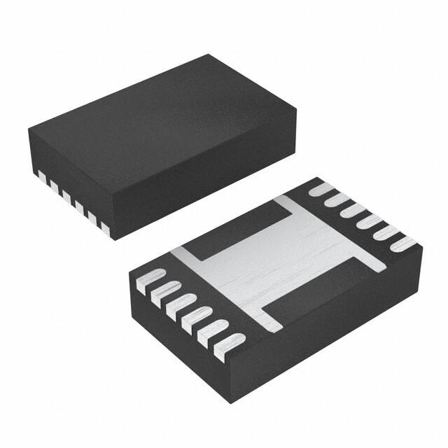
The small, 12-pin, 2.50 mm × 4.00 mm, Small Outline
No-Lead (SON) package is ideal for spaceconstrained applications.
Device Information(1)
PART NUMBER
PACKAGE
bq27411-G1
Smartphones, Feature Phones, and Tablets
Digital Still and Video Cameras
Handheld Terminals
MP3 or Multimedia Players
2.50 mm x 4.00 mm
(1) For all available packages, see the orderable addendum at
the end of the data sheet.
Simplified Schematic
2 Applications
•
•
•
•
BODY SIZE (NOM)
VSON (12)
Battery Pack
PACKP
PROG
OTP
Data
1.0 MΩ
SRN
Coulomb
Counter
Diff. Input
1
Current
ADC
I 2 C Bus
SDA
SDA
SCL
SCL
I-Wake
CPU
TEST
Voltage
ADC
Die Temp
Sensor
1.0 MΩ
BAT
10 mΩ,
1% shunt
SRP
BAT
1.8V
LDO
VSS
VDD
0.47 µF
Li- Ion
Cell
1 µF
Protection IC
PACKN
FET
FET
Copyright © 2017, Texas Instruments Incorporated
1
An IMPORTANT NOTICE at the end of this data sheet addresses availability, warranty, changes, use in safety-critical applications,
intellectual property matters and other important disclaimers. PRODUCTION DATA.
�bq27411-G1
SLUSBN7D – JANUARY 2014 – REVISED APRIL 2017
www.ti.com
Table of Contents
1
2
3
4
5
6
7
Features ..................................................................
Applications ...........................................................
Description .............................................................
Revision History.....................................................
Device Comparison Table.....................................
Pin Configuration and Functions .........................
Specifications.........................................................
1
1
1
2
3
3
4
7.1
7.2
7.3
7.4
7.5
7.6
7.7
4
4
4
4
5
5
Absolute Maximum Ratings ......................................
ESD Ratings ............................................................
Recommended Operating Conditions.......................
Thermal Information ..................................................
Supply Current ..........................................................
Digital Input and Output DC Characteristics .............
LDO Regulator, Wake-Up, and Auto-Shutdown DC
Characteristics ...........................................................
7.8 ADC (Temperature and Cell Measurement)
Characteristics ...........................................................
7.9 Integrating ADC (Coulomb Counter) Characteristics
7.10 I2C-Compatible Interface Communication Timing
Characteristics ...........................................................
7.11 Typical Characteristics ............................................
5
5
6
6
7
8
Detailed Description .............................................. 8
8.1
8.2
8.3
8.4
8.5
9
Overview ...................................................................
Functional Block Diagram .........................................
Feature Description...................................................
Device Functional Modes..........................................
Programming.............................................................
8
8
8
9
9
Applications and Implementation ...................... 13
9.1 Application Information............................................ 13
9.2 Typical Applications ................................................ 13
10 Power Supply Recommendation ....................... 16
10.1 Power Supply Decoupling ..................................... 16
11 Layout................................................................... 17
11.1 Layout Guidelines ................................................. 17
11.2 Layout Example .................................................... 18
12 Device and Documentation Support ................. 19
12.1
12.2
12.3
12.4
Documentation Support ........................................
Trademarks ...........................................................
Electrostatic Discharge Caution ............................
Glossary ................................................................
19
19
19
19
13 Mechanical, Packaging, and Orderable
Information ........................................................... 19
4 Revision History
NOTE: Page numbers for previous revisions may differ from page numbers in the current version.
Changes from Revision C (September 2015) to Revision D
Page
•
Changed Simplified Schematic .............................................................................................................................................. 1
•
Changed Pin Functions PROG description ........................................................................................................................... 3
•
Changed Figure 5 ................................................................................................................................................................ 13
•
Changed Figure 6 ................................................................................................................................................................ 14
•
Changed Power Supply Decoupling .................................................................................................................................... 16
•
Changed Layout Guidelines ................................................................................................................................................ 17
•
Changed Figure 10 .............................................................................................................................................................. 18
2
Submit Documentation Feedback
Copyright © 2014–2017, Texas Instruments Incorporated
Product Folder Links: bq27411-G1
�bq27411-G1
www.ti.com
SLUSBN7D – JANUARY 2014 – REVISED APRIL 2017
5 Device Comparison Table
PART NUMBER
BATTERY TYPE
CHEM_ID (1)
DM_CODE (2)
bq27411DRZR-G1A
LiCoO2
(4.2-V maximum charge)
0x0128
0x80
LiCoO2
(4.3-V maximum charge)
0x0312
0x90
LiCoO2
(4.35-V maximum charge)
0x0354
0xA0
bq27411DRZT-G1A
bq27411DRZR-G1B
bq27411DRZT-G1B
bq27411DRZR-G1C
bq27411DRZT-G1C
(1)
(2)
(3)
FIRMWARE
VERSION (3)
1.09
(0x0109)
Refer to the CHEM_ID subcommand to confirm the battery chemistry type.
Refer to the DM_CODE subcommand to confirm the Data Memory code.
Refer to the FW_VERSION subcommand to confirm the firmware version.
6 Pin Configuration and Functions
SDA
1
12
PROG
SCL
2
11
NC
V
3
10
TEST
4
9
NC
5
8
SRP
6
7
SRN
SS
NC
V
DD
BAT
Not to scale
Pin Functions
NUMBER
NAME
TYPE (1)
1
SDA
DIO
2
SCL
DIO
3
VSS
PI
Ground pin
4
NC
—
No internal connection. May be left floating or tied to VSS.
5
VDD
PO
1.8-V Regulator Output. Decouple with 0.47-μF ceramic capacitor to VSS. This pin is not intended to provide
power for other devices in the system.
6
BAT
PI, AI
7
SRN
AI
8
SRP
AI
9
NC
—
No internal connection. May be left floating or tied to VSS.
10
TEST
DI
This digital factory TEST pin must be pulled low for proper operation in customer's application. Recommend
terminating with a 1.0-MΩ (typical) pulldown resistor to VSS for reduced power consumption.
11
NC
—
No internal connection. May be left floating or tied to VSS.
DO
Programming voltage input for the One Time Programmable (OTP) memory to be used during customer
factory configuration. To avoid a floating input condition, recommend terminating with a 1.0-MΩ (typical)
pulldown resistor to VSS for reduced power consumption.
If the device is in SHUTDOWN mode, toggling PROG causes the gauge exit SHUTDOWN. It is recommended
to connect PROG to the SDA line through a 470-KΩ resistor, so that in case of any inadvertent shutdown
condition, the gauge can be commanded to come out of SHUTDOWN.
12
(1)
PROG
DESCRIPTION
Slave I2C serial bus for communication with system (Master). Open-drain pins. Use with external 5- to 10-kΩ
pullup resistors (typical) for each pin. If the external pullup resistors will be disconnected from these pins
during normal operation, recommend using external 1.0-MΩ pulldown resistors to VSS at each pin to avoid
floating inputs.
LDO regulator input, battery voltage input, and coulomb counter input typically connected to the PACK+
terminal. Connect a capacitor (1 µF) between BAT to VSS. Place the capacitor close to gauge.
Coulomb counter differential inputs expecting an external 10-mΩ, 1% sense resistor. Connect SRP to BAT
(CELLP) and connect SRN to PACKP.
Low-side current sensing can be enabled by connecting SRN to BATN and SRP to PACKN.
Refer to the typical application diagrams in Typical Applications.
DIO = Digital input-output, AI = Analog input, P = Power connection
Submit Documentation Feedback
Copyright © 2014–2017, Texas Instruments Incorporated
Product Folder Links: bq27411-G1
3
�bq27411-G1
SLUSBN7D – JANUARY 2014 – REVISED APRIL 2017
www.ti.com
7 Specifications
7.1 Absolute Maximum Ratings
over operating free-air temperature range (unless otherwise noted) (1)
VBAT
VSR
MIN
MAX
UNIT
BAT pin input voltage range
–0.3
6
V
SRP and SRN pins input voltage range
–0.3
VBAT + 0.3
V
2
V
2
V
Differential voltage across SRP and SRN. ABS(SRP–SRN)
VDD
VDD pin supply voltage range (LDO output)
–0.3
VIOD
Open-drain IO pins (SDA, SCL)
–0.3
6
V
VPROG
PROG (pin 12)
–0.3
7.8
V
VIOPP
Push-pull IO pins (TEST, pin 10)
–0.3
VDD + 0.3
V
TA
Operating free-air temperature range
–40
85
°C
Tstg
Storage temperature
–65
150
°C
(1)
Stresses beyond those listed under "absolute maximum ratings" may cause permanent damage to the device. These are stress ratings
only, and functional operation of the device at these or any other conditions beyond those indicated under "recommended operating
conditions" is not implied. Exposure to absolute-maximum-rated conditions for extended periods may affect device reliability.
7.2 ESD Ratings
VALUE
V(ESD)
(1)
(2)
Electrostatic discharge
Human-body model (HBM), per ANSI/ESDA/JEDEC JS-001 (1)
±1500
Charged-device model (CDM), per JEDEC specification JESD22C101 (2)
±250
UNIT
V
JEDEC document JEP155 states that 500-V HBM allows safe manufacturing with a standard ESD control process.
JEDEC document JEP157 states that 250-V CDM allows safe manufacturing with a standard ESD control process.
7.3 Recommended Operating Conditions
TA = 30°C and VREGIN = VBAT = 3.6 V (unless otherwise noted)
MIN
CBAT (1)
External input capacitor for internal
LDO between BAT and VSS
CLDO18 (1)
External output capacitor for internal
LDO between VDD and VSS
VPU (1)
External pull-up voltage for opendrain pins (SDA, SCL, PROG)
VPV
PROG Programming Voltage [RA0]
IPV
PROG Programming Current [RA0]
(1)
Nominal capacitor values specified.
Recommend a 5% ceramic X5R
type capacitor located close to the
device.
NOM
UNIT
0.1
μF
0.47
μF
1.62
TA = 15°C to 35°C. OTP
Programming mode only.
MAX
7.3
3.6
V
7.4
7.5
V
4
5
mA
Specified by design. Not production tested.
7.4 Thermal Information
THERMAL METRIC (1)
bq27411-G1
DRZ (12 PINS)
RθJA
Junction-to-ambient thermal resistance
64.1
RθJC(top)
Junction-to-case (top) thermal resistance
59.8
RθJB
Junction-to-board thermal resistance
52.7
ψJT
Junction-to-top characterization parameter
0.3
ψJB
Junction-to-board characterization parameter
28.3
RθJC(bot)
Junction-to-case (bottom) thermal resistance
2.4
(1)
4
UNIT
°C/W
For more information about traditional and new thermal metrics, see the IC Package Thermal Metrics Application Report, SPRA953.
Submit Documentation Feedback
Copyright © 2014–2017, Texas Instruments Incorporated
Product Folder Links: bq27411-G1
�bq27411-G1
www.ti.com
SLUSBN7D – JANUARY 2014 – REVISED APRIL 2017
7.5 Supply Current
TA = 30°C and VREGIN = VBAT = 3.6 V (unless otherwise noted)
PARAMETER
ICC
(1)
TEST CONDITIONS
MAX
UNIT
μA
21
μA
9
μA
0.6
μA
ILOAD > Sleep Current
SLEEP mode current
ILOAD < Sleep Current (2)
IHIB (1)
HIBERNATE mode current
ILOAD < Hibernate Current (2)
SHUTDOWN mode current
Fuel gauge in host-commanded
SHUTDOWN mode.
(LDO regulator output disabled)
(1)
(2)
TYP
93
NORMAL mode current
ISLP (1)
ISD (1)
MIN
(2)
Specified by design. Not production tested.
Wake Comparator Disabled
7.6 Digital Input and Output DC Characteristics
TA = –40°C to 85°C, typical values at TA = 30°C and VREGIN = 3.6 V (unless otherwise noted)
PARAMETER
TEST CONDITIONS
VIH(OD)(For Input voltage, high (2)
ce
Note1) (1)
VIH(PP)
Input voltage, high (3)
VIL
Input voltage, low (2) (3)
MIN
TYP
MAX
UNIT
External pullup resistor to VPU
VPU × 0.7
V
1.4
V
0.6
(2)
V
VOL
Output voltage, low
0.6
V
IOH
Output source current, high (2)
0.5
mA
IOL(OD)
Output sink current, low (2)
–3
mA
5
pF
CIN
(1)
Input leakage current (2) (3)
Ilkg
(1)
(2)
(3)
Input capacitance
(2) (3)
SCL, SDA, and TEST pins
0.1
PROG pin
1.0
μA
Specified by design. Not production tested.
Open Drain pins: (SCL, SDA, PROG)
Push-pull pin: (TEST)
7.7 LDO Regulator, Wake-Up, and Auto-Shutdown DC Characteristics
TA = –40°C to 85°C, typical values at TA = 30°C and VREGIN = 3.6 V (unless otherwise noted)(Force Note1) (1)
PARAMETER
VBAT
BAT pin regulator input
VDD
Regulator output voltage
UVLOIT+
VBAT Undervoltage lockout
LDO Wake-up rising threshold
UVLOIT–
VBAT Undervoltage lockout
LDO Auto-shutdown falling threshold
(1)
TEST CONDITIONS
MIN
TYP
2.45
MAX
UNIT
4.5
V
1.8
V
2
V
1.95
V
Specified by design. Not production tested.
7.8 ADC (Temperature and Cell Measurement) Characteristics
TA = –40°C to 85°C; typical values at TA = 30°C and VREGIN = 3.6 V (unless otherwise noted) (Force Note1) (1)
PARAMETER
VIN(BAT)
BAT pin voltage measurement range
tADC_CONV
Conversion time
TEST CONDITIONS
Voltage divider enabled
Effective Resolution
(1)
MIN
TYP
2.45
MAX
UNIT
4.5
V
125
ms
15
bits
Specified by design. Not tested in production.
Submit Documentation Feedback
Copyright © 2014–2017, Texas Instruments Incorporated
Product Folder Links: bq27411-G1
5
�bq27411-G1
SLUSBN7D – JANUARY 2014 – REVISED APRIL 2017
www.ti.com
7.9 Integrating ADC (Coulomb Counter) Characteristics
TA = –40°C to 85°C; typical values at TA = 30°C and VREGIN = 3.6 V (unless otherwise noted)(Force Note1) (1)
PARAMETER
TEST CONDITIONS
MIN
TYP
MAX
VSR
Input voltage range from BAT to SRX pins
tSR_CONV
Conversion time
Single conversion
1
s
Effective Resolution
Single conversion
16
bits
(1)
BAT ± 25
UNIT
mV
Specified by design. Not tested in production.
7.10 I2C-Compatible Interface Communication Timing Characteristics
TA = –40°C to 85°C; typical values at TA = 30°C and VREGIN = 3.6 V (unless otherwise noted)
MIN
TYP
MAX
UNIT
Standard Mode (100 kHz)
td(STA)
(Force
Note1) (1)
Start to first falling edge of SCL
tw(L)
SCL pulse duration (low)
tw(H)
SCL pulse duration (high)
tsu(STA)
Setup for repeated start
tsu(DAT)
Data setup time
th(DAT)
Data hold time
tsu(STOP)
Setup time for stop
t(BUF)
Bus free time between stop and start Includes command waiting time
tf
SCL or SDA fall time
tr
SCL or SDA rise time
fSCL
4
μs
Clock frequency
4.7
μs
4
μs
4.7
μs
Host drives SDA
250
ns
Host drives SDA
0
ns
4
μs
66
(1)
μs
300
(1)
(2)
ns
300
ns
100
kHz
Fast Mode (400 kHz)
td(STA)
Start to first falling edge of SCL
600
ns
tw(L)
SCL pulse duration (low)
1300
ns
tw(H)
SCL pulse duration (high)
600
ns
tsu(STA)
Setup for repeated start
600
ns
tsu(DAT)
Data setup time
Host drives SDA
100
ns
th(DAT)
Data hold time
Host drives SDA
0
ns
tsu(STOP)
Setup time for stop
600
ns
t(BUF)
Bus free time between stop and start Includes command waiting time
tf
SCL or SDA fall time
tr
SCL or SDA rise time
fSCL
(1)
(2)
6
Clock frequency
(1)
(1)
(2)
66
μs
300
ns
300
ns
400
kHz
Specified by design. Not production tested.
If the clock frequency (fSCL) is > 100 kHz, use 1-byte write commands for proper operation. All other transactions types are supported at
400 kHz. (See I2C Interface and I2C Command Waiting Time.)
Submit Documentation Feedback
Copyright © 2014–2017, Texas Instruments Incorporated
Product Folder Links: bq27411-G1
�bq27411-G1
www.ti.com
SLUSBN7D – JANUARY 2014 – REVISED APRIL 2017
tSU(STA)
tw(H)
tf
tw(L)
tr
t(BUF)
SCL
SDA
td(STA)
tsu(STOP)
tf
tr
th(DAT)
tsu(DAT)
REPEATED
START
STOP
START
Figure 1. I2C-Compatible Interface Timing Diagrams
7.11 Typical Characteristics
0.14
10
0.12
5
Temperature Accuracy Error(%)
Voltage Accuracy Error (%)
0.1
0.08
0.06
0
-5
-10
0.04
0.02
-40
-20
0
20
40
Temperature (°C)
60
80
100
-15
-40
-20
Figure 2. Voltage Accuracy
0
20
40
Temperature (°C)
60
80
100
Figure 3. Temperature Accuracy
0
-0.1
Current Accuracy Error (%)
-0.2
-0.3
-0.4
-0.5
-0.6
-40
-20
0
20
40
Temperature (°C)
60
80
100
Figure 4. Current Accuracy
Submit Documentation Feedback
Copyright © 2014–2017, Texas Instruments Incorporated
Product Folder Links: bq27411-G1
7
�bq27411-G1
SLUSBN7D – JANUARY 2014 – REVISED APRIL 2017
www.ti.com
8 Detailed Description
8.1 Overview
The bq27411-G1 fuel gauge accurately predicts the battery capacity and other operational characteristics of a
single Li-based rechargeable cell. It can be interrogated by a system processor to provide cell information, such
as state-of-charge (SOC). The fuel gauge is available in several options optimized for different battery cell
chemistries (see Device Comparison Table). Configuration parameters unique to the customer's application are
programmed in OTP memory at the customer's factory using a 7.4-V typical voltage applied to the PROG pin and
a set of I2C programming commands. More details are available in the SmartFlash OTP Programming
Application Report (SLUA703).
NOTE
Formatting Conventions used in this Document:
Commands: italics with parentheses() and no breaking spaces; for example, Control()
Data Flash: italics, bold, and breaking spaces; for example, Design Capacity
Register bits and flags: italics with brackets [ ]; for example, [TDA]
Data flash bits: italics, bold, and brackets [ ]; for example, [LED1]
Modes and states: ALL CAPITALS; for example, UNSEALED mode
8.2 Functional Block Diagram
Battery Pack
PACKP
PROG
1.0 MΩ
SRN
Coulomb
Counter
Diff. Input
OTP
Data
Current
ADC
I 2 C Bus
SDA
SDA
I-Wake
SCL
SCL
CPU
TEST
Voltage
ADC
Die Temp
Sensor
1.0 MΩ
BAT
10 mΩ,
1% shunt
SRP
BAT
1.8V
LDO
VSS
VDD
0.47 µF
Li- Ion
Cell
1 µF
Protection IC
PACKN
FET
FET
Copyright © 2017, Texas Instruments Incorporated
8.3 Feature Description
Information is accessed through a series of commands, called Standard Commands. Further capabilities are
provided by the additional Extended Commands set. Both sets of commands, indicated by the general format
Command(), are used to read and write information contained within the control and status registers, as well as
its data locations.
8
Submit Documentation Feedback
Copyright © 2014–2017, Texas Instruments Incorporated
Product Folder Links: bq27411-G1
�bq27411-G1
www.ti.com
SLUSBN7D – JANUARY 2014 – REVISED APRIL 2017
Feature Description (continued)
The key to the high-accuracy gas gauging prediction is Texas Instruments proprietary Impedance Track
algorithm. This algorithm uses cell measurements, characteristics, and properties to create state-of-charge
predictions that can achieve high accuracy across a wide variety of operating conditions and over the lifetime of
the battery.
The fuel gauge measures the charging or discharging of the battery by monitoring the voltage across a smallvalue sense resistor. When a cell is attached to the fuel gauge, cell impedance is computed, based on cell
current, cell open-circuit voltage (OCV), and cell voltage under loading conditions.
The fuel gauge uses an integrated temperature sensor for estimating cell temperature. Alternatively, the host
processor can provide temperature data for the fuel gauge.
For more details, see the bq27411-G1 Technical Reference Manual (SLUUAS7).
8.4 Device Functional Modes
To minimize power consumption, the fuel gauge has several power modes: INITIALIZATION, NORMAL, SLEEP,
and HIBERNATE. The fuel gauge passes automatically between these modes, depending upon the occurrence
of specific events, though a system processor can initiate some of these modes directly.
For more details, see the bq27411-G1 Technical Reference Manual (SLUUAS7).
8.5 Programming
8.5.1 Standard Data Commands
The bq27411-G1 fuel gauge uses a series of 2-byte standard commands to enable system reading and writing of
battery information. Each standard command has an associated command-code pair, as indicated in Table 1.
Because each command consists of two bytes of data, two consecutive I2C transmissions must be executed both
to initiate the command function, and to read or write the corresponding two bytes of data. For more details, see
the bq27411-G1 Technical Reference Manual (SLUUAS7).
Table 1. Standard Commands
NAME
COMMAND
CODE
UNIT
SEALED
ACCESS
Control()
CNTL
0x00 and 0x01
NA
R/W
Temperature()
TEMP
0x02 and 0x03
0.1°K
R/W
Voltage()
VOLT
0x04 and 0x05
mV
R
FLAGS
0x06 and 0x07
NA
R
0x08 and 0x09
mAh
R
Flags()
NominalAvailableCapacity()
FullAvailableCapacity()
0x0A and 0x0B
mAh
R
RemainingCapacity()
RM
0x0C and 0x0D
mAh
R
FullChargeCapacity()
FCC
0x0E and 0x0F
mAh
R
AverageCurrent()
0x10 and 0x11
mA
R
StandbyCurrent()
0x12 and 0x13
mA
R
MaxLoadCurrent()
0x14 and 0x15
mA
R
AveragePower()
0x18 and 0x19
mW
R
0x1C and 0x1D
%
R
0x1E and 0x1F
0.1°K
R
0x20 and 0x21
num / %
R
RemainingCapacityUnfiltered()
0x28 and 0x29
mAh
R
RemainingCapacityFiltered()
0x2A and 0x2B
mAh
R
FullChargeCapacityUnfiltered()
0x2C and 0x2D
mAh
R
FullChargeCapacityFiltered()
0x2E and 0x2F
mAh
R
StateOfChargeUnfiltered()
0x30 and 0x31
%
R
StateOfCharge()
SOC
InternalTemperature()
StateOfHealth()
SOH
Submit Documentation Feedback
Copyright © 2014–2017, Texas Instruments Incorporated
Product Folder Links: bq27411-G1
9
�bq27411-G1
SLUSBN7D – JANUARY 2014 – REVISED APRIL 2017
www.ti.com
8.5.2 Control(): 0x00 and 0x01
Issuing a Control() command requires a subsequent 2-byte subcommand. These additional bytes specify the
particular control function desired. The Control() command allows the system to control specific features of the
fuel gauge during normal operation and additional features when the device is in different access modes, as
described in Table 2. For additional details, see the bq27411-G1 Technical Reference Manual (SLUUAS7).
Table 2. Control() Subcommands
CONTROL
DATA
SEALED ACCESS
CONTROL_STATUS
0x0000
Yes
Reports the status of device
DEVICE_TYPE
0x0001
Yes
Reports the device type (0x0421)
FW_VERSION
0x0002
Yes
Reports the firmware version of the device
DM_CODE
0x0004
Yes
Reports the Data Memory Code number stored in OTP memory
PREV_MACWRITE
0x0007
Yes
Returns previous MAC command code
CHEM_ID
0x0008
Yes
Reports the chemical identifier of the battery profile currently
used by the Impedance Track configuration
SET_HIBERNATE
0x0011
Yes
Forces CONTROL_STATUS [HIBERNATE] to 1
CLEAR_HIBERNATE
0x0012
Yes
Forces CONTROL_STATUS [HIBERNATE] to 0
SET_CFGUPDATE
0x0013
No
Forces CONTROL_STATUS [CFGUPMODE] to 1 and gauge
enters CONFIG UPDATE mode
SEALED
0x0020
No
Places the device in SEALED access mode
RESET
0x0041
No
Performs a full device reset
SOFT_RESET
0x0042
No
Gauge exits CONFIG UPDATE mode
CONTROL FUNCTION
DESCRIPTION
8.5.3 Extended Data Commands
Extended data commands offer additional functionality beyond the standard set of commands. They are used in
the same manner; however, unlike standard commands, extended commands are not limited to 2-byte words.
The number of command bytes for a given extended command ranges in size from single to multiple bytes, as
specified in Table 3.
Table 3. Extended Commands
Name
OpConfig()
DesignCapacity()
DataClass()
(2)
DataBlock()
(2)
Command Code
Unit
SEALED
Access (1) (2)
UNSEALED
Access (1) (2)
0x3A and 0x3B
NA
R
R
0x3C and 0x3D
mAh
R
R
0x3E
NA
NA
RW
0x3F
NA
RW
RW
0x40 through 0x5F
NA
R
RW
BlockDataCheckSum()
0x60
NA
RW
RW
BlockDataControl()
0x61
NA
NA
RW
0x62 through 0x7F
NA
R
R
BlockData()
Reserved
(1)
(2)
SEALED and UNSEALED states are entered via commands to Control() 0x00 and 0x01
In SEALED mode, data cannot be accessed through commands 0x3E and 0x3F.
8.5.4 Communications
8.5.4.1 I2C Interface
The bq27411-G1 fuel gauge supports the standard I2C read, incremental read, quick read, one-byte write, and
incremental write functions. The 7-bit device address (ADDR) is the most significant 7 bits of the hex address
and is fixed as 1010101. The first 8 bits of the I2C protocol are, therefore, 0xAA or 0xAB for write or read,
respectively.
10
Submit Documentation Feedback
Copyright © 2014–2017, Texas Instruments Incorporated
Product Folder Links: bq27411-G1
�bq27411-G1
www.ti.com
SLUSBN7D – JANUARY 2014 – REVISED APRIL 2017
Host generated
S
ADDR[6:0]
0 A
Gauge generated
CMD [7:0]
A
DATA [7:0]
A P
S
ADDR[6:0]
(a) 1-byte write
S
ADDR[6:0]
0 A
1 A
DATA [7:0]
N P
(b) quick read
CMD [7:0]
A Sr
ADDR[6:0]
1 A
DATA [7:0]
N P
(c) 1- byte read
S
ADDR[6:0]
0 A
CMD [7:0]
A Sr
ADDR[6:0]
1 A
DATA [7:0]
A ...
DATA [7:0]
N P
(d) incremental read
S
ADDR[6:0]
0 A
CMD[7:0]
A
DATA [7:0]
A
DATA [7:0]
A
...
A P
(e) incremental write
(S = Start , Sr = Repeated Start , A = Acknowledge , N = No Acknowledge , and P = Stop).
The quick read returns data at the address indicated by the address pointer. The address pointer, a register
internal to the I2C communication engine, increments whenever data is acknowledged by the fuel gauge or the
I2C master. “Quick writes” function in the same manner and are a convenient means of sending multiple bytes to
consecutive command locations (such as two-byte commands that require two bytes of data).
The following command sequences are not supported:
Attempt to write a read-only address (NACK after data sent by master):
Attempt to read an address above 0x6B (NACK command):
8.5.4.2 I2C Time Out
The I2C engine releases both SDA and SCL if the I2C bus is held low for 2 seconds. If the fuel gauge is holding
the lines, releasing them frees them for the master to drive the lines. If an external condition is holding either of
the lines low, the I2C engine enters the low-power SLEEP mode.
8.5.4.3 I2C Command Waiting Time
To ensure proper operation at 400 kHz, a t(BUF) ≥ 66-μs bus-free waiting time must be inserted between all
packets addressed to the fuel gauge. In addition, if the SCL clock frequency (fSCL) is > 100 kHz, use individual 1byte write commands for proper data flow control. The following diagram shows the standard waiting time
required between issuing the control subcommand the reading the status result. For read-write standard
command, a minimum of 2 seconds is required to get the result updated. For read-only standard commands,
there is no waiting time required, but the host must not issue any standard command more than two times per
second. Otherwise, the gauge could result in a reset issue due to the expiration of the watchdog timer.
Submit Documentation Feedback
Copyright © 2014–2017, Texas Instruments Incorporated
Product Folder Links: bq27411-G1
11
�bq27411-G1
SLUSBN7D – JANUARY 2014 – REVISED APRIL 2017
www.ti.com
S
ADDR [6:0]
0 A
CMD [7:0]
A
DATA [7:0]
A P
66ms
S
ADDR [6:0]
0 A
CMD [7:0]
A
DATA [7:0]
A P
66ms
S
ADDR [6:0]
0 A
CMD [7:0]
A Sr
ADDR [6:0]
1 A
DATA [7:0]
A
DATA [7:0]
N P
66ms
N P
66ms
Waiting time inserted between two 1-byte write packets for a subcommand and reading results
(required for 100 kHz < fSCL £ 400 kHz)
S
ADDR [6:0]
0 A
CMD [7:0]
A
DATA [7:0]
S
ADDR [6:0]
0 A
CMD [7:0]
A Sr
ADDR [6:0]
A
1 A
DATA [7:0]
A P
DATA [7:0]
A
66ms
DATA [7:0]
Waiting time inserted between incremental 2-byte write packet for a subcommand and reading results
(acceptable for fSCL £ 100 kHz)
S
ADDR [6:0]
DATA [7:0]
0 A
A
CMD [7:0]
DATA [7:0]
A Sr
N P
ADDR [6:0]
1 A
DATA [7:0]
A
DATA [7:0]
A
66ms
Waiting time inserted after incremental read
8.5.4.4 I2C Clock Stretching
A clock stretch of up to 4 ms can occur during all modes of fuel gauge operation. In SLEEP and HIBERNATE
modes, a short ≤ 100-µs clock stretch occurs on all I2C traffic as the device must wake-up to process the packet.
In the other modes (INITIALIZATION, NORMAL) a ≤ 4-ms clock stretching period may occur within packets
addressed for the fuel gauge. The majority of clock stretch periods are small while the I2C interface performs
normal data flow control.
12
Submit Documentation Feedback
Copyright © 2014–2017, Texas Instruments Incorporated
Product Folder Links: bq27411-G1
�bq27411-G1
www.ti.com
SLUSBN7D – JANUARY 2014 – REVISED APRIL 2017
9 Applications and Implementation
NOTE
Information in the following application section is not part of the TI component
specification, and TI does not warrant its accuracy or completeness. TI’s customers are
responsible for determining suitability of components for their purposes. Customers should
validate and test their design implementation to confirm system functionality.
9.1 Application Information
The bq27411-G1 device is a fuel gauging solution for single-cell Li-Ion battery packs. The device requires
minimal configuration and uses One Time Programmable (OTP) Non-Volatile Memory (NVM) to avoid an
initialization download by the system processor. To allow for optimal performance in the end application, special
considerations must be taken to ensure minimization of measurement error through proper printed circuit board
(PCB) board layout. Such requirements are detailed in Design Requirements.
9.2 Typical Applications
SDA
SC L
Optional ESD Filter
C4
R6
1M
150 pF
R10
100
R11
100
R7
300
R8
300
R9
1M
PGND
C5
150 pF
PGND
TP1
PROG
U1
SD A
2
NC
SC L
VSS
NC
5
SRP
BAT
PWPD
VD D
C1
R4
1.0 M
PGND
NC 9
4
6
11
TEST 10
3
PG ND
R5
1.0 M
PROG 12
1
PGND
8
SRN 7
13
0.47 µF
PG ND
PG N D
J2
R1
1
J1
CELLP
1
CELLN
2
0. 010
Note: 1% Tolerance
1
2
C2
1.0 µF
SDA
2
SCL
3
4
PACKP
SDA
SCL
Note: SDA and SCL
Require 5 Kohm
pullups provided by
system
PACKN
PGND
Figure 5. Typical Application with High-Side Current Sense Resistor
Submit Documentation Feedback
Copyright © 2014–2017, Texas Instruments Incorporated
Product Folder Links: bq27411-G1
13
�bq27411-G1
SLUSBN7D – JANUARY 2014 – REVISED APRIL 2017
www.ti.com
Typical Applications (continued)
SDA
SC L
Optional ESD Filter
C4
R6
1M
150 pF
R10
100
R11
100
R7
300
R8
300
R9
1M
PGND
C5
150 pF
PGND
TP1
PROG
U1
2
3
4
5
PG ND
6
C1
SD A
PROG
SC L
NC
VSS
TEST
NC
NC
SRP
VD D
PWPD
1
BAT
SRN
R5
1.0 M
12
11
R4
1.0 M
PGND
10
9
8
PGND
7
13
0.47 µF
PG ND
PG N D
J2
1
J1
CELLP
CELLN
1
2
1
SDA
C2
1.0 µF
2
SCL
2
3
R1
4
PGND
PACKP
SDA
SCL
Note: SDA and SCL
Require 5-KΩ
pullups provided by
the system
PACKN
0. 010
Note: 1% Tolerance
Figure 6. Typical Application with Low-Side Current Sense Resistor
9.2.1 Design Requirements
As shipped from the Texas Instruments factory, many bq27411-G1 parameters in OTP NVM are left in the
unprogrammed state (zero) while some parameters directly associated with the CHEMID are preprogrammed.
This partially programmed configuration facilitates customization for each end application. Upon device reset, the
contents of OTP are copied to associated volatile RAM-based Data Memory blocks. For proper operation, all
parameters in RAM-based Data Memory require initialization—either by updating Data Memory parameters in a
lab/evaluation situation or by programming the OTP for customer production. Chapter 5 in the bq27411-G1
Technical Reference Manual (SLUUAS7) shows the default value and a typically expected value appropriate for
most applications.
9.2.2 Detailed Design Procedure
9.2.2.1 High-Side or Low-Side Sense Resistor
The bq27411-G1 device can be used with a high-side current resistor, as shown in Figure 5 or a low-side current
resistor, as shown in Figure 6.
9.2.2.2 BAT Voltage Sense Input
A ceramic capacitor at the input to the BAT pin is used to bypass AC voltage ripple to ground, greatly reducing
its influence on battery voltage measurements. It proves most effective in applications with load profiles that
exhibit high-frequency current pulses (that is, cell phones) but is recommended for use in all applications to
reduce noise on this sensitive high-impedance measurement node.
14
Submit Documentation Feedback
Copyright © 2014–2017, Texas Instruments Incorporated
Product Folder Links: bq27411-G1
�bq27411-G1
www.ti.com
SLUSBN7D – JANUARY 2014 – REVISED APRIL 2017
Typical Applications (continued)
9.2.2.3 Sense Resistor Selection
Any variation encountered in the resistance present between the SRP and SRN pins of the fuel gauge will affect
the resulting differential voltage, and derived current, it senses. As such, it is recommended to select a sense
resistor with minimal tolerance and temperature coefficient of resistance (TCR) characteristics. The standard
recommendation based on best compromise between performance and price is a 1% tolerance, 50-ppm drift
sense resistor with a 1-W power rating.
9.2.2.4 Communication Interface Lines
A protection network composed of resistors and capacitors is recommended on each of the serial communication
inputs to protect the fuel gauge from dangerous ESD transients.
9.2.3 Application Curves
0.14
10
0.12
5
Temperature Accuracy Error(%)
Voltage Accuracy Error (%)
0.1
0.08
0.06
0
-5
-10
0.04
0.02
-40
-20
0
20
40
Temperature (°C)
60
80
100
-15
-40
-20
Figure 7. Voltage Accuracy
0
20
40
Temperature (°C)
60
80
100
Figure 8. Temperature Accuracy
0
-0.1
Current Accuracy Error (%)
-0.2
-0.3
-0.4
-0.5
-0.6
-40
-20
0
20
40
Temperature (°C)
60
80
100
Figure 9. Current Accuracy
Submit Documentation Feedback
Copyright © 2014–2017, Texas Instruments Incorporated
Product Folder Links: bq27411-G1
15
�bq27411-G1
SLUSBN7D – JANUARY 2014 – REVISED APRIL 2017
www.ti.com
10 Power Supply Recommendation
10.1 Power Supply Decoupling
The battery connection on the BAT pin is used for two purposes:
• To supply power to the fuel gauge
• As an input for voltage measurement of the battery
A capacitor of value of at least 1 µF should be connected between BAT and VSS. The capacitor should be placed
close to the gauge IC and have short traces to both the VDD pin and VSS.
The fuel gauge has an integrated LDO with an output on the VDD pin of approximately 1.8 V. A capacitor of value
at least 0.47 μF should be connected between the VDD pin and VSS. The capacitor should be placed close to the
gauge IC and have short traces to both the VDD pin and VSS.
16
Submit Documentation Feedback
Copyright © 2014–2017, Texas Instruments Incorporated
Product Folder Links: bq27411-G1
�bq27411-G1
www.ti.com
SLUSBN7D – JANUARY 2014 – REVISED APRIL 2017
11 Layout
11.1 Layout Guidelines
•
•
•
•
A capacitor, of value at least 0.47 µF, is connected between the VDD pin and VSS. The capacitor should be
placed close to the gauge IC and have short traces to both the VDD pin and VSS.
It is required to have a capacitor, at least 1.0 µF, connect between the BAT pin and VSS if the connection
between the battery pack and the gauge BAT pin has the potential to pick up noise. The capacitor should be
placed close to the gauge IC and have short traces to both the VDD pin and VSS.
If the external pullup resistors on the SCL and SDA lines will be disconnected from the host during low-power
operation, it is recommended to use external 1-MΩ pulldown resistors to VSS to avoid floating inputs to the I2C
engine.
The value of the SCL and SDA pullup resistors should take into consideration the pullup voltage and the bus
capacitance. Some recommended values, assuming a bus capacitance of 10 pF, can be seen in Table 4.
Table 4. Recommended Values for SCL and SDA Pullup Resistors
VPU
RPU
•
•
•
•
1.8 V
3.3 V
Range
Typical
Range
Typical
400 Ω ≤ RPU ≤ 37.6 kΩ
10 kΩ
900 Ω ≤ RPU ≤ 29.2 kΩ
5.1 kΩ
If the GPOUT pin is not used by the host, the pin should still be pulled up to VDD with a 4.7-kΩ or 10-kΩ
resistor. After the OTP has been programmed, it is recommended that PROG be connected to the SDA line
with a 470-KΩ resistor so that in cases where the device is in SHUTDOWN, toggling PROG can wake the
gauge up from the SHUTDOWN state.
If the battery pack thermistor is not connected to the BIN pin, the BIN pin should be pulled down to VSS with a
10-kΩ resistor.
The BIN pin should not be shorted directly to VDD or VSS.
The actual device ground is the center pin (B2). The C1 pin is floating internally and can be used as a bridge
to connect the board ground plane to the device ground (B2).
Submit Documentation Feedback
Copyright © 2014–2017, Texas Instruments Incorporated
Product Folder Links: bq27411-G1
17
�bq27411-G1
SLUSBN7D – JANUARY 2014 – REVISED APRIL 2017
www.ti.com
11.2 Layout Example
Battery Pack
10 mΩ 1%
PACKP
Use copper pours for
battery power path to
minimize IR losses
Kelvin connect SRP and
SRN connections right at
Rsense terminals
SRN
Kelvin connect BAT sense
line right at positive
battery terminal
BAT
CBAT
VDD
VDD
SRP
CVDD
+
PROG
NC
NC
TS
RTHERM
RESD2
RESD1
RESD4
RESD3
TEST
VSS
NC
SCL
PROG
SDA
1 MΩ
Place close
to gauge IC.
Trace to pin
and VSS
should be
short.
SDA
SCL
1 MΩ
Star ground right at
PACK– for ESD
return path
Protection
IC
Use short and wide
traces to minimize
inductance
NFET
PACKN
NFET
Via connects to Power Ground
Figure 10. bq27411-G1 Board Layout
18
Submit Documentation Feedback
Copyright © 2014–2017, Texas Instruments Incorporated
Product Folder Links: bq27411-G1
�bq27411-G1
www.ti.com
SLUSBN7D – JANUARY 2014 – REVISED APRIL 2017
12 Device and Documentation Support
12.1 Documentation Support
12.1.1 Related Documentation
• bq27411-G1 Technical Reference Manual (SLUUAS7)
• bq27411 EVM: Single-Cell Technology User's Guide (SLUUAP3)
• SmartFlash OTP Programming (SLUA703)
• Quickstart Guide for bq27411-G1 (SLUUAP6)
• Single Cell Gas Gauge Circuit Design (SLUA456)
• Key Design Considerations for the bq27500 and bq27501 (SLUA439)
• Single Cell Impedance Track Printed-Circuit Board Layout Guide (SLUA457)
• ESD and RF Mitigation in Handheld Battery Electronics (SLUA460)
12.1.2 Community Resources
The following links connect to TI community resources. Linked contents are provided "AS IS" by the respective
contributors. They do not constitute TI specifications and do not necessarily reflect TI's views; see TI's Terms of
Use.
TI E2E™ Online Community TI's Engineer-to-Engineer (E2E) Community. Created to foster collaboration
among engineers. At e2e.ti.com, you can ask questions, share knowledge, explore ideas and help
solve problems with fellow engineers.
Design Support TI's Design Support Quickly find helpful E2E forums along with design support tools and
contact information for technical support.
12.2 Trademarks
Impedance Track, E2E are trademarks of Texas Instruments.
I2C is a trademark of NXP B.V. Corporation.
All other trademarks are the property of their respective owners.
12.3 Electrostatic Discharge Caution
This integrated circuit can be damaged by ESD. Texas Instruments recommends that all integrated circuits be handled with
appropriate precautions. Failure to observe proper handling and installation procedures can cause damage.
ESD damage can range from subtle performance degradation to complete device failure. Precision integrated circuits may be more
susceptible to damage because very small parametric changes could cause the device not to meet its published specifications.
12.4 Glossary
SLYZ022 — TI Glossary.
This glossary lists and explains terms, acronyms, and definitions.
13 Mechanical, Packaging, and Orderable Information
The following pages include mechanical, packaging, and orderable information. This information is the most
current data available for the designated devices. This data is subject to change without notice and revision of
this document. For browser-based versions of this data sheet, refer to the left-hand navigation.
Submit Documentation Feedback
Copyright © 2014–2017, Texas Instruments Incorporated
Product Folder Links: bq27411-G1
19
�PACKAGE OPTION ADDENDUM
www.ti.com
6-Feb-2020
PACKAGING INFORMATION
Orderable Device
Status
(1)
Package Type Package Pins Package
Drawing
Qty
Eco Plan
Lead/Ball Finish
MSL Peak Temp
(2)
(6)
(3)
Op Temp (°C)
Device Marking
(4/5)
BQ27411DRZR-G1A
ACTIVE
SON
DRZ
12
3000
Green (RoHS
& no Sb/Br)
NIPDAU
Level-2-260C-1 YEAR
-40 to 85
BQ27
411A
BQ27411DRZR-G1C
ACTIVE
SON
DRZ
12
3000
Green (RoHS
& no Sb/Br)
NIPDAU
Level-2-260C-1 YEAR
-40 to 85
BQ27
411C
BQ27411DRZT-G1A
ACTIVE
SON
DRZ
12
250
Green (RoHS
& no Sb/Br)
NIPDAU
Level-2-260C-1 YEAR
-40 to 85
BQ27
411A
BQ27411DRZT-G1C
ACTIVE
SON
DRZ
12
250
Green (RoHS
& no Sb/Br)
NIPDAU
Level-2-260C-1 YEAR
-40 to 85
BQ27
411C
(1)
The marketing status values are defined as follows:
ACTIVE: Product device recommended for new designs.
LIFEBUY: TI has announced that the device will be discontinued, and a lifetime-buy period is in effect.
NRND: Not recommended for new designs. Device is in production to support existing customers, but TI does not recommend using this part in a new design.
PREVIEW: Device has been announced but is not in production. Samples may or may not be available.
OBSOLETE: TI has discontinued the production of the device.
(2)
RoHS: TI defines "RoHS" to mean semiconductor products that are compliant with the current EU RoHS requirements for all 10 RoHS substances, including the requirement that RoHS substance
do not exceed 0.1% by weight in homogeneous materials. Where designed to be soldered at high temperatures, "RoHS" products are suitable for use in specified lead-free processes. TI may
reference these types of products as "Pb-Free".
RoHS Exempt: TI defines "RoHS Exempt" to mean products that contain lead but are compliant with EU RoHS pursuant to a specific EU RoHS exemption.
Green: TI defines "Green" to mean the content of Chlorine (Cl) and Bromine (Br) based flame retardants meet JS709B low halogen requirements of


 工商网监
湘ICP备2023018690号
工商网监
湘ICP备2023018690号

