Product
Folder
Order
Now
Support &
Community
Tools &
Software
Technical
Documents
BQ27510-G3
SLUSAT1B – MARCH 2013 – REVISED MARCH 2020
BQ27510-G3 System-Side Impedance Track™ Fuel Gauge With Direct Battery Connection
1 Features
2 Applications
•
•
•
•
•
•
•
1
•
•
•
Single-series cell li-ion battery fuel gauge resides
on system board
– Integrated 2.5-VDC LDO
– External low-value 10-mΩ sense resistor
Patented Impedance Track™ technology
– Adjusts for battery aging, self-discharge,
temperature, and rate changes
– Reports remaining capacity, state-of-Charge
(SOC), and time-to-empty
– Optional smoothing filter
– Battery state-of-health (aging) estimation
– Supports embedded or removable packs with
up to 32-Ah capacity
– Accommodates pack swapping with 2
separate battery profiles
Microcontroller Peripheral Supports:
– 400-kHz I2C serial interface
– 32 bytes of scratch-pad FLASH NVM
– Battery low digital output warning
– Configurable SOC interrupts
– External thermistor, internal sensor, or hostreported temperature options
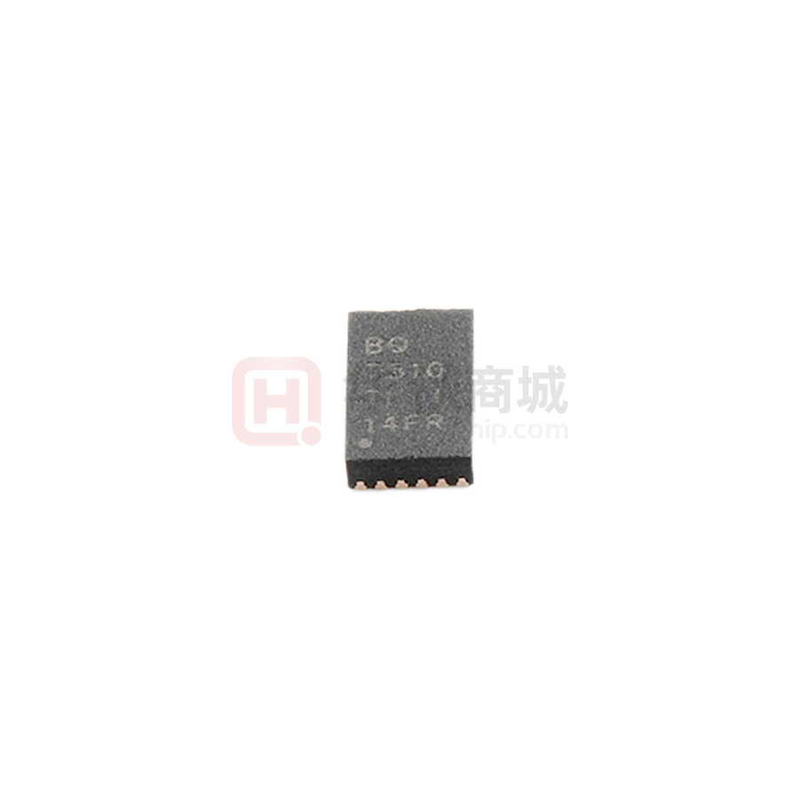
Small 12-pin 2.50 mm × 4.00 mm SON package
Smartphones, Feature Phones, and Tablets
Wearables
Building Automation
Portable Medical/Industrial Handsets
Portable Audio
Gaming
3 Description
The Texas Instruments BQ27510-G3 system-side LiIon battery fuel gauge is a microcontroller peripheral
that provides fuel gauging for single-cell Li-Ion battery
packs.
The
device
requires
little
system
microcontroller firmware development. The BQ27510G3 resides on the system’s main board and manages
an embedded battery (non-removable) or a
removable battery pack.
The BQ27510-G3 uses the patented Impedance
Track™ algorithm for fuel gauging, and provides
information, such as remaining battery capacity
(mAh), state-of-charge (%), run-time to empty (min.),
battery voltage (mV), temperature (°C) and state-ofhealth (%).
Battery fuel gauging with the BQ27510-G3 requires
only PACK+ (P+), PACK– (P–), and optional
Thermistor (T) connections to a removable battery
pack or embedded battery circuit.
Device Information(1)
PART NUMBER
BQ27510-G3
FIRMWARE
VERSION
PACKAGE
SON (12)
4.00 (0X0400)
(1) For all available packages, see the orderable addendum at
the end of the data sheet.
Simplified Schematic
Host System
Single-Cell Li-ion
Battery Pack
VCC
REG25
Power
Management
Controller
2
IC
LDO
REGIN
PACK+
GPOUT
Voltage
Sense
DATA
Temp
Sense
PROTECTION
IC
T
bq27510-G3
PACK-
FETs
CHG
DSG
Current
Sense
1
An IMPORTANT NOTICE at the end of this data sheet addresses availability, warranty, changes, use in safety-critical applications,
intellectual property matters and other important disclaimers. PRODUCTION DATA.
�BQ27510-G3
SLUSAT1B – MARCH 2013 – REVISED MARCH 2020
www.ti.com
Table of Contents
1
2
3
4
5
6
Features ..................................................................
Applications ...........................................................
Description .............................................................
Revision History.....................................................
Pin Configuration and Functions .........................
Specifications.........................................................
1
1
1
2
3
3
6.1
6.2
6.3
6.4
6.5
6.6
6.7
3
4
4
4
5
6
Absolute Maximum Ratings ......................................
ESD Ratings..............................................................
Recommended Operating Conditions.......................
Thermal Information ..................................................
Electrical Characteristics ..........................................
Data Flash Memory Characteristics..........................
400-kHz I2C-Compatible Interface Communication
Timing Requirements.................................................
6.8 100-kHz I2C-Compatible Interface Communication
Timing Requirements.................................................
6.9 Typical Characteristics ..............................................
7
6
6
7
Detailed Description .............................................. 8
7.1 Overview ................................................................... 8
7.2 Functional Block Diagram ......................................... 9
7.3 Feature Description................................................. 10
7.4 Device Functional Modes........................................ 10
7.5 Programming........................................................... 13
8
Application and Implementation ........................ 17
8.1 Application Information............................................ 17
8.2 Typical Application ................................................. 17
9
Power Supply Recommendations...................... 20
9.1 Power Supply Decoupling ....................................... 20
10 Layout................................................................... 21
10.1 Layout Guidelines ................................................. 21
10.2 Layout Example .................................................... 21
11 Device and Documentation Support ................. 22
11.1 Documentation Support ........................................ 22
11.2 Receiving Notification of Documentation Updates
.................................................................................22
11.3 Support Resources ............................................... 22
11.4 Trademarks ........................................................... 22
11.5 Electrostatic Discharge Caution ............................ 22
11.6 Glossary ................................................................ 22
12 Mechanical, Packaging, and Orderable
Information ........................................................... 22
4 Revision History
NOTE: Page numbers for previous revisions may differ from page numbers in the current version.
Changes from Revision A (November 2015) to Revision B
Page
•
Changed Table 2 ................................................................................................................................................................. 13
•
Changed I2C Command Waiting Time ................................................................................................................................ 15
Changes from Original (March 2013) to Revision A
•
2
Page
Added ESD Ratings table, Feature Description section, Device Functional Modes, Application and Implementation
section, Power Supply Recommendations section, Layout section, Device and Documentation Support section, and
Mechanical, Packaging, and Orderable Information section. ................................................................................................ 1
Submit Documentation Feedback
Copyright © 2013–2020, Texas Instruments Incorporated
Product Folder Links: BQ27510-G3
�BQ27510-G3
www.ti.com
SLUSAT1B – MARCH 2013 – REVISED MARCH 2020
5 Pin Configuration and Functions
DRZ Package
12-Pin SON
Top View
BI/TOUT
1
12
GPOUT
REG25
2
11
SCL
REGIN
3
10
SDA
BAT
4
9
TS
Vcc
5
8
SRN
Vss
6
7
SRP
Pin Functions
PIN
NAME
NO.
TYPE (1)
DESCRIPTION
Battery-insertion detection input. Power pin for pack thermistor network. Thermistor-multiplexer control
pin. Open-drain I/O. Use with pull-up resistor >1MΩ (1.8 MΩ typical).
BI/TOUT
1
I/O
REG25
2
P
2.5-V output voltage of the internal integrated LDO
REGIN
3
P
Regulator input. Decouple with 0.1-μF ceramic capacitor to Vss
BAT
4
I
Cell voltage measurement input. ADC input
Vcc
5
P
Processor power input. Decouple with 0.1-μF ceramic capacitor minimum
Vss
6
P
Device ground
SRP
7
IA
Analog input pin connected to the internal coulomb counter with a Kelvin connection where SRP is
nearest the PACK– connection. Connect to 5-mΩ to 20-mΩ sense resistor.
SRN
8
IA
Analog input pin connected to the internal coulomb counter with a Kelvin connection where SRN is
nearest the Vss connection. Connect to 5-mΩ to 20-mΩ sense resistor.
TS
9
IA
Pack thermistor voltage sense (use 103AT-type thermistor). ADC input
SDA
10
I/O
Slave I2C serial communications data line for communication with system (Master). Open-drain I/O.
Use with 10-kΩ pull-up resistor (typical).
SCL
11
I
Slave I2C serial communications clock input line for communication with system (Master). Open-drain
I/O. Use with 10-kΩ pull-up resistor (typical).
GPOUT
12
O
General Purpose open-drain output. May be configured as Battery Low, Battery Good, or to perform
interrupt functionality.
(1)
I/O = Digital input/output; IA = Analog input; P = Power connection.
6 Specifications
6.1 Absolute Maximum Ratings
over operating free-air temperature range (unless otherwise noted) (1)
MIN
MAX
UNIT
VREGIN
Regulator input voltage
–0.3
24
V
VCC
Supply voltage
–0.3
2.75
V
VIOD
Open-drain I/O pins (SDA, SCL, GPOUT)
–0.3
6
V
VBAT
BAT input pin
–0.3
6
V
VI
Input voltage to all other pins (TS, SRP, SRN, BI/TOUT)
–0.3
VCC + 0.3
V
TF
Functional temperature
–40
100
°C
Tstg
Storage temperature
–65
150
°C
(1)
Stresses beyond those listed under Absolute Maximum Ratings may cause permanent damage to the device. These are stress ratings
only, which do not imply functional operation of the device at these or any other conditions beyond those indicated under Recommended
Operating Conditions. Exposure to absolute-maximum-rated conditions for extended periods may affect device reliability.
Submit Documentation Feedback
Copyright © 2013–2020, Texas Instruments Incorporated
Product Folder Links: BQ27510-G3
3
�BQ27510-G3
SLUSAT1B – MARCH 2013 – REVISED MARCH 2020
www.ti.com
6.2 ESD Ratings
VALUE
Human-body model (HBM), per
ANSI/ESDA/JEDEC JS-001 (1)
V(ESD)
Electrostatic discharge
All pins except pin 4
±2000
Pin 4
±1500
Charged-device model (CDM), per JEDEC specification JESD22C101 (2)
(1)
(2)
UNIT
V
±250
JEDEC document JEP155 states that 500-V HBM allows safe manufacturing with a standard ESD control process.
JEDEC document JEP157 states that 250-V CDM allows safe manufacturing with a standard ESD control process.
6.3 Recommended Operating Conditions
TA = 25°C, VCC = 2.5 V (unless otherwise noted)
MIN
Supply voltage
VREGIN
No operating restrictions
CREG25
External REG25 capacitor
tPUCD
Power Up Communication Delay
NOM
MAX
2.7
5.5
No FLASH writes
2.45
2.7
CREG25
0.47
UNIT
V
µF
250
ms
103
μA
Normal operating mode current
Fuel gauge in NORMAL mode
ILOAD > Sleep Current
Low-power operating mode current
Fuel gauge in SLEEP mode
ILOAD < Sleep Current
18
μA
Low-power operating mode current
Fuel gauge in SLEEP+ mode
ILOAD < Sleep Current
60
μA
Hibernate operating mode current
Fuel gauge in HIBERNATE mode
ILOAD < Hibernate Current
4
μA
VOL
Output voltage low (SDA, GPOUT, BI/TOUT)
IOL = 0.5 mA
VOH(PP)
Output high voltage (GPOUT)
IOH = –1 mA
VCC–0.5
VOH(OD)
Output high voltage (SDA, SCL, BI/TOUT)
External pull-up resistor connected to Vcc
VCC–0.5
ICC
ISLP
ISLP+
IHIB
Input voltage low (SDA, SCL)
VIL
Input voltage low (BI/TOUT)
BAT INSERT CHECK MODE active
Input voltage high (SDA, SCL)
VIH(OD)
Input voltage high (BI/TOUT)
BAT INSERT CHECK MODE active
0.4
V
V
V
–0.3
0.6
–0.3
0.6
1.2
6
1.2
6
V
V
VA1
Input voltage range (TS)
VSS–0.125
2
V
VA2
Input voltage range (BAT)
VSS–0.125
5
V
VA3
Input voltage range (SRP, SRN)
VSS–0.125
tPUCD
Power-up communication delay
TA
Operating free-air temperature
0.125
250
–40
V
ms
85
°C
6.4 Thermal Information
BQ27510-G3
THERMAL METRIC (1)
DRZ (SON)
UNIT
12 PINS
RθJA
Junction-to-ambient thermal resistance
64.1
°C/W
RθJC(top)
Junction-to-case (top) thermal resistance
59.8
°C/W
RθJB
Junction-to-board thermal resistance
52.7
°C/W
ψJT
Junction-to-top characterization parameter
0.3
°C/W
ψJB
Junction-to-board characterization parameter
28.3
°C/W
RθJC(bot)
Junction-to-case (bottom) thermal resistance
2.4
°C/W
(1)
4
For more information about traditional and new thermal metrics, see the Semiconductor and IC Package Thermal Metrics application
report, SPRA953.
Submit Documentation Feedback
Copyright © 2013–2020, Texas Instruments Incorporated
Product Folder Links: BQ27510-G3
�BQ27510-G3
www.ti.com
SLUSAT1B – MARCH 2013 – REVISED MARCH 2020
6.5 Electrical Characteristics
TA = 25°C, CREG = 0.47 μF, VREGIN = 3.6 V (unless otherwise noted)
PARAMETER
2.5-V LDO
TEST CONDITION
MIN
NOM
MAX
2.5
2.6
VREG25
Regulator output voltage
2.7 V ≤ VREGIN ≤ 5.5 V,
IOUT ≤ 16mA
TA = –40°C to 85°C
2.4
2.45 V ≤ VREGIN < 2.7 V (low
battery), IOUT ≤ 3mA
TA = –40°C to 85°C
2.4
2.7 V, IOUT ≤ 16 mA
TA = –40°C to 85°C
280
Regulator dropout voltage
ΔVREGTEMP
Regulator output change
with temperature
VREGIN = 3.6 V, IOUT = 16 mA
ΔVREGLINE
Line regulation
2.7 V ≤ VREGIN ≤ 5.5 V, IOUT = 16 mA
11
25
Load regulation
0.2 mA ≤ IO UT ≤ 3 mA, VREGIN = 2.45 V
34
40
3 mA ≤ IOUT ≤ 16 mA, VREGIN = 2.7 V
31
ΔVREGLOAD
(2)
Short circuit current limit
2.45 V, IOUT ≤ 3 mA
VREG25 = 0 V
V
V
VDO
ISHORT
UNIT
(1)
mV
50
TA = –40°C to 85°C
0.3%
TA = –40°C to 85°C
mV
mV
250
mA
POWER-ON RESET
VIT+
Positive-going battery
voltage input at VCC
TA = –40°C to 85°C
2.05
2.20
2.31
V
VHYS
Power-on reset hysteresis
TA = –40°C to 85°C
45
115
185
mV
INTERNAL TEMPERATURE SENSOR CHARACTERISTICS
GTEMP
Temperature sensor voltage TA = –40°C to 85°C, 2.4 V < VCC < 2.6 V; typical
gain
values at TA = 25°C and VCC = 2.5 V
–2
mV/°C
INTERNAL CLOCK OSCILLATORS
fOSC
fLOSC
High Frequency Oscillator
TA = –40°C to 85°C, 2.4 V < VCC < 2.6 V; typical
values at TA = 25°C and VCC = 2.5 V
8.389
MHz
Low Frequency Oscillator
TA = –40°C to 85°C, 2.4 V < VCC < 2.6 V; typical
values at TA = 25°C and VCC = 2.5 V
32.768
kHz
INTEGRATING ADC (COULOMB COUNTER) CHARACTERISTICS
Input voltage range, V(SRN)
and V(SRP)
VSR = V(SRN) – V(SRP)
Conversion time
Single conversion
Resolution
TA = –40°C to 85°C, 2.4 V < VCC < 2.6 V
Input offset
TA = 25°C and VCC = 2.5 V
Integral nonlinearity error
TA = –40°C to 85°C, 2.4 V < VCC < 2.6 V
ZSR_IN
Effective input resistance (2)
TA = –40°C to 85°C, 2.4 V < VCC < 2.6 V
ISR_LKG
Input leakage current (2)
TA = –40°C to 85°C, 2.4 V < VCC < 2.6 V
VSR_IN
tSR_CONV
VSR_OS
INL
TA = –40°C to
85°C, 2.4 V < VCC
< 2.6 V
–0.125
TA = 25°C and VCC
= 2.5 V
0.125
1
14
s
15
10
±0.007
%
V
bits
µV
±0.034
%
2.5
FSR
MΩ
0.3
µA
ADC (TEMPERATURE AND CELL MEASUREMENT) CHARACTERISTICS
VADC_IN
Input voltage range
TA = –40°C to 85°C, 2.4 V < VCC < 2.6 V
tADC_CONV
Conversion time
TA = –40°C to 85°C, 2.4 V < VCC < 2.6 V
Resolution
TA = –40°C to 85°C, 2.4 V < VCC < 2.6 V
VADC_OS
Input offset
TA = 25°C and VCC = 2.5 V
ZADC1
Effective input resistance
(TS) (2)
TA = –40°C to 85°C, 2.4 V < VCC < 2.6 V
8
MΩ
Effective input resistance
(BAT) (2)
BQ27510-G3 not measuring cell TA = –40°C to
voltage
85°C, 2.4 V < VCC
< 2.6 V
8
MΩ
ZADC2
BQ27510-G3 measuring cell
voltage
(1)
(2)
–0.2
1
14
ms
15
bits
1
TA = 25°C and VCC
= 2.5 V
V
125
100
mV
kΩ
LDO output current, IOUT, is the sum of internal and external load currents.
Assured by design. Not production tested.
Submit Documentation Feedback
Copyright © 2013–2020, Texas Instruments Incorporated
Product Folder Links: BQ27510-G3
5
�BQ27510-G3
SLUSAT1B – MARCH 2013 – REVISED MARCH 2020
www.ti.com
Electrical Characteristics (continued)
TA = 25°C, CREG = 0.47 μF, VREGIN = 3.6 V (unless otherwise noted)
PARAMETER
IADC_LKG
Input leakage current
TEST CONDITION
(2)
MIN
NOM
TA = –40°C to 85°C, 2.4 V < VCC < 2.6 V
MAX
0.3
UNIT
µA
6.6 Data Flash Memory Characteristics
TA = –40°C to 85°C, 2.4 V < VCC < 2.6 V; typical values at TA = 25°C and VCC = 2.5 V (unless otherwise noted)
PARAMETER
TEST CONDITIONS
Data retention (1)
tDR
TYP
MAX
10
Flash programming write-cycles
(1)
Word programming time
ICCPROG)
Flash-write supply current (1)
UNIT
Years
20,000
Cycles
(1)
tWORDPROG)
(1)
MIN
5
2
ms
10
mA
Assured by design. Not production tested.
6.7 400-kHz I2C-Compatible Interface Communication Timing Requirements
TA = –40°C to 85°C, 2.4 V < VCC < 2.6 V; typical values at TA = 25°C and VCC = 2.5 V (unless otherwise noted)
PARAMETER
TEST CONDITIONS
MIN
TYP
MAX
UNIT
tr
SCL/SDA rise time
300
ns
tf
SCL/SDA fall time
300
ns
tw(H)
SCL pulse width (high)
600
ns
tw(L)
SCL pulse width (low)
1.3
μs
tsu(STA)
Setup for repeated start
600
ns
td(STA)
Start to first falling edge of SCL
600
ns
tsu(DAT)
Data setup time
100
ns
th(DAT)
Data hold time
tsu(STOP)
Setup time for stop
tBUF
Bus free time between stop and start
fSCL
Clock frequency
0
ns
600
ns
66
μs
400
kHz
MAX
UNIT
6.8 100-kHz I2C-Compatible Interface Communication Timing Requirements
TA = –40°C to 85°C, 2.4 V < VCC < 2.6 V; typical values at TA = 25°C and VCC = 2.5 V (unless otherwise noted)
PARAMETER
tr
SCL/SDA rise time
tf
SCL/SDA fall time
tw(H)
SCL pulse width (high)
tw(L)
TEST CONDITIONS
MIN
TYP
1
300
µs
ns
4
µs
SCL pulse width (low)
4.7
μs
tsu(STA)
Setup for repeated start
4.7
µs
td(STA)
Start to first falling edge of SCL
4
µs
tsu(DAT)
Data setup time
250
ns
th(DAT)
Data hold time
tsu(STOP)
Setup time for stop
tBUF
Bus free time between stop and start
fSCL
Clock frequency
tBUSERR
Bus error timeout
6
Receive mode
0
Transmit mode
300
Submit Documentation Feedback
ns
4
µs
4.7
μs
10
100
kHz
17.3
21.2
s
Copyright © 2013–2020, Texas Instruments Incorporated
Product Folder Links: BQ27510-G3
�BQ27510-G3
www.ti.com
SLUSAT1B – MARCH 2013 – REVISED MARCH 2020
tSU(STA)
tw(H)
tf
tw(L)
tr
t(BUF)
SCL
SDA
td(STA)
tsu(STOP)
tf
tr
th(DAT)
tsu(DAT)
REPEATED
START
STOP
START
Figure 1. I2C-Compatible Interface Timing Diagram
2.58
32.8
2.56
32.75
2.54
32.7
L F O (kH Z )
R E G 2 5 O u tp u t (V )
6.9 Typical Characteristics
2.52
2.5
2.48
32.6
32.55
2.46
2.44
-40
32.65
32.5
I OUT = 16 mA, REGIN = 5 V
I OUT = 3 mA, REGIN = 2.7 V
-20
0
20
40
Temperature (qC)
60
80
32.45
-40
100
-20
0
20
40
Temperature (qC)
D001
Figure 2. REG25 vs. Temperature
60
80
100
D002
Figure 3. Low Frequency Oscillator vs. Temperature
8.4
8.395
H F O (M H Z )
8.39
8.385
8.38
8.375
8.37
8.365
-40
-20
0
20
40
Temperature (qC)
60
80
100
D003
Figure 4. High Frequency Oscillator vs. Temperature
Submit Documentation Feedback
Copyright © 2013–2020, Texas Instruments Incorporated
Product Folder Links: BQ27510-G3
7
�BQ27510-G3
SLUSAT1B – MARCH 2013 – REVISED MARCH 2020
www.ti.com
7 Detailed Description
7.1 Overview
The BQ27510-G3 fuel gauge accurately predicts the battery capacity and other operational characteristics of a
single Li-based rechargeable cell. It can be interrogated by a system processor to provide cell information, such
as time-to-empty (TTE) and state-of-charge (SOC) as well as SOC interrupt signal to the host.
Information is accessed through a series of commands, called Standard Commands. Further capabilities are
provided by the additional Extended Commands set. Both sets of commands, indicated by the general format
Command(), read and write information contained within the device control and status registers, as well as its
data flash locations. Commands are sent from system to gauge using the I2C serial communications engine, and
can be executed during application development, system manufacture, or end-equipment operation.
Cell information is stored in the device in non-volatile flash memory. Many of these data flash locations are
accessible during application development. They cannot, generally, be accessed directly during end-equipment
operation. Access to these locations is achieved by either use of the fuel gauge companion evaluation software,
through individual commands, or through a sequence of data-flash-access commands. To access a desired data
flash location, the correct data flash subclass and offset must be known.
The key to the fuel gauge high-accuracy gas gauging prediction is Texas Instruments proprietary Impedance
Track™ algorithm. This algorithm uses cell measurements, characteristics, and properties to create state-ofcharge predictions that can achieve less than 1% error across a wide variety of operating conditions and over the
lifetime of the battery.
The fuel gauge measures charge and discharge activity by monitoring the voltage across a small-value series
sense resistor (5 mΩ to 20 mΩ, typical) located between the system VSS and the battery PACK– terminal. When
a cell is attached to the device, cell impedance is learned, based on cell current, cell open-circuit voltage (OCV),
and cell voltage under loading conditions.
The external temperature sensing is optimized with the use of a high-accuracy negative temperature coefficient
(NTC) thermistor with R25 = 10.0 kΩ ±1%. B25/85 = 3435 kΩ ± 1% (such as Semitec NTC 103AT). Alternatively,
the fuel gauge can also be configured to use its internal temperature sensor or receive temperature data from the
host processor. When an external thermistor is used, a 18.2-kΩ pull-up resistor between BI/TOUT and TS pins is
also required. The fuel gauge uses temperature to monitor the battery-pack environment, which is used for fuel
gauging and cell protection functionality.
To minimize power consumption, the fuel gauge has several power modes: NORMAL, SLEEP, HIBERNATE, and
BAT INSERT CHECK. The fuel gauge passes automatically between these modes, depending upon the
occurrence of specific events, though a system processor can initiate some of these modes directly.
For complete operational details, refer to the BQ27510-G3 Technical Reference Manual, BQ27510-G3 SystemSide Impedance Track™ Fuel Gauge With Integrated LDO, SLUUA97.
Table 1. Formatting Conventions Used in This Document
INFORMATION TYPE
FORMATTING CONVENTION
EXAMPLE
Commands
Italics with parentheses and no breaking spaces
RemainingCapacity() command
NVM Data
Italics, bold, and breaking spaces
Design Capacity data
Register bits and flags
Brackets and italics
[TDA] bit
NVM Data bits
Brackets, italics, and bold
[LED1] bit
Modes and states
ALL CAPITALS
UNSEALED mode
8
Submit Documentation Feedback
Copyright © 2013–2020, Texas Instruments Incorporated
Product Folder Links: BQ27510-G3
�BQ27510-G3
www.ti.com
SLUSAT1B – MARCH 2013 – REVISED MARCH 2020
7.2 Functional Block Diagram
REGIN
LDO
POR
REG25
2.5 V
VCC
HFO
BAT
CC
HFO
SRN
LFO
HFO/128
4R
HFO/128
SRP
MUX
ADC
R
Wake
Comparator
TS
Internal
Temp
Sensor
BI/TOUT
HFO/4
SDA
GPOUT
22
I2C Slave
Engine
Instruction
ROM
22
CPU
VSS
SCL
I/O
Controller
Instruction
FLASH
8
Wake
and
Watchdog
Timer
GP Timer
and
PWM
Data
SRAM
8
Data
FLASH
Submit Documentation Feedback
Copyright © 2013–2020, Texas Instruments Incorporated
Product Folder Links: BQ27510-G3
9
�BQ27510-G3
SLUSAT1B – MARCH 2013 – REVISED MARCH 2020
www.ti.com
7.3 Feature Description
The fuel gauge measures the cell voltage, temperature, and current to determine battery SOC. The fuel gauge
monitors charge and discharge activity by sensing the voltage across a small-value (5 mΩ to 20 mΩ typical)
resistor between the SRP and SRN pins and in series with the cell. By integrating charge passing through the
battery, the battery’s SOC is adjusted during battery charge or discharge.
The total battery capacity is found by comparing states of charge before and after applying the load with the
amount of charge passed. When an application load is applied, the impedance of the cell is measured by
comparing the OCV obtained from a predefined function for present SOC with the measured voltage under load.
Measurements of OCV and charge integration determine chemical state of charge and chemical capacity
(Qmax). The initial Qmax values are taken from a cell manufacturers' data sheet multiplied by the number of
parallel cells. It is also used for the value in Design Capacity. The fuel gauge acquires and updates the battery
impedance profile during normal battery usage. It uses this profile, along with SOC and the Qmax value, to
determine FullChargeCapacity() and StateOfCharge(), specifically for the present load and temperature.
FullChargeCapacity() is reported as capacity available from a fully charged battery under the present load and
temperature until Voltage() reaches the Terminate Voltage. NominalAvailableCapacity() and
FullAvailableCapacity() are the uncompensated (no or light load) versions of RemainingCapacity() and
FullChargeCapacity() respectively.
The fuel gauge has two flags accessed by the Flags() function that warns when the battery’s SOC has fallen to
critical levels. When StateOfCharge() falls below the first capacity threshold, specified in SOC1 Set Threshold,
the [SOC1] (State of Charge Initial) flag is set. The flag is cleared once StateOfCharge() rises above SOC1 Clear
Threshold. The fuel gauge’s GPOUT pin puts out 3 pulses 10ms wide and in 10ms intervals whenever the
SOC1 flag is set. This flag is enabled when RMC_IND bit in Operation Configuration B is set. This behavior
also applies to the [SOCF] (State of Charge Final) flag.
When Voltage() falls below the system shut down threshold voltage, SysDown Set Volt Threshold, the
[SYSDOWN] flag is set, serving as a final warning to shut down the system. The GPOUT also signals. When
Voltage() rises above SysDown Clear Voltage and the [SYSDOWN] flag has already been set, the [SYSDOWN]
flag is cleared. The GPOUT also signals such change. All units are in mV. Additional details are found in the
BQ27510-G3 Technical Reference Manual, BQ27510-G3 System-Side Impedance Track™ Fuel Gauge With
Integrated LDO, SLUUA97.
7.4 Device Functional Modes
7.4.1 Power Modes
The fuel gauge has different power modes: BAT INSERT CHECK, NORMAL, SNOOZE, SLEEP, and
HIBERNATE. In NORMAL mode, the fuel gauge is fully powered and can execute any allowable task. In
SNOOZE mode, both low-frequency and high-frequency oscillators are active. Although the SNOOZE mode has
higher current consumption than the SLEEP mode, it is also a reduced-power mode. In SLEEP mode, the fuel
gauge turns off the high-frequency oscillator and exists in a reduced-power state, periodically taking
measurements and performing calculations. In HIBERNATE mode, the fuel gauge is in a low-power state, but
can be woken up by communication or certain IO activity. Finally, the BAT INSERT CHECK mode is a powered
up, but low-power halted, state, where the fuel gauge resides when no battery is inserted into the system.
Figure 5 and Figure 6 show the relationship between these modes.
10
Submit Documentation Feedback
Copyright © 2013–2020, Texas Instruments Incorporated
Product Folder Links: BQ27510-G3
�BQ27510-G3
www.ti.com
SLUSAT1B – MARCH 2013 – REVISED MARCH 2020
Device Functional Modes (continued)
POR
Exit From HIBERNATE
Battery Removed
bq27510 clears CONTROL_STATUS
[HIBERNATE] = 0
Recommend Host also set
CONTROL_STATUS
[HEBERNATE] = 0
Exit From SLEEP
Flags [BAT_DET] = 0
BAT INSERT CHECK
Exit From HIBERNATE
Communication Activity
AND Comm address is for bq27510
Check for battery insertion
from HALT state.
No gauging
Entry To NORMAL
Flags [BAT_DET] = 1
Flags [BAT_DET] = 0
Exit From NORMAL
Flags [BAT_DET] = 0
NORMAL
Fuel gauging and data
updated every second.
HIBERNATE
Wakeup From HIBERNATE
Communication Activity
AND
Comm address is not for
bq27510
Disable all bq27510
subcircuits except GPIO
Negate BAT_GD
Exit From WAIT_HIBERNATE
Host must set CONTROL_STATUS
[HIBERNATE] = 0
AND
VCELL < Hibernate Voltage
To SLEEP
WAIT_HIBERNATE
Exit From WAIT_HIBERNATE
Cell relaxed
AND
Ι AverageCurrent () Ι < Hibernate
Current
OR
Cell relaxed
AND
VCELL < Hibernate Voltage
Fuel gauging and data
updated every 20 seconds.
BAT_GD unchanged.
Exit From SLEEP
Host has set CONTROL_STATUS
[HIBERNATE] = 1
OR
VCELL < Hibernate Voltage
System Shutdown
Figure 5. Power Mode Diagram for System Shutdown
Submit Documentation Feedback
Copyright © 2013–2020, Texas Instruments Incorporated
Product Folder Links: BQ27510-G3
11
�BQ27510-G3
SLUSAT1B – MARCH 2013 – REVISED MARCH 2020
www.ti.com
Device Functional Modes (continued)
Exit From HIBERNATE
Battery Removed
POR
BAT INSERT CHECK
Exit From HIBERNATE
Communication Activity
AND Comm address is for bq27510
bq27510 clears CONTROL_STATUS
[HIBERNATE] = 0
Recommend Host also set
CONTROL_STATUS
[HEBERNATE] = 0
Check for battery insertion
from HALT state.
No gauging
Entry To NORMAL
Flags [BAT_DET] = 1
Exit From NORMAL
Flags [BAT_DET] = 0
NORMAL
Entry To SNOOZE
Operation Configuration [SLEEP] = 1
AND
CONTROL_STATUS [SNOOZE] = 1]
AND
Ι AverageCurrent ( ) Ι < Sleep Current
Flags [BAT_DET] = 0
Fuel gauging and data
updated every second
Exit From SLEEP
Flags [BAT_DET] = 0
Exit From SLEEP
Ι AverageCurrent ( ) Ι > Sleep Current
OR
Current is detected above Ι WAKE
Exit From SNOOZE
Any communication to the gauge
OR
Ι AverageCurrent ( ) Ι > Sleep Current
OR
Current is detected above Ι WAKE
SNOOZE
Entry To SLEEP
Operation Configuration [SLEEP] = 1
AND
CONTROL_STATUS [SNOOZE] = 0]
AND
Ι AverageCurrent ( ) Ι < Sleep Current
Fuel gauging and data
updated every 20 seconds.
Both LFO and HFO are ON.
Entry to SNOOZE
CONTROL_STATUS [SNOOZE] = 1
Entry to SLEEP
CONTROL_STATUS [SNOOZE] = 0
SLEEP
Fuel gauging and data
updated every 20 seconds.
(LFO ON and HFO OFF)
Exit From WAIT_HIBERNATE
Host must set CONTROL_STATUS
[HIBERNATE] = 0
AND
VCELL < Hibernate Voltage
To WAIT_HIBERNATE
System Sleep
Exit From SLEEP
Host has set CONTROL_STATUS
[HIBERNATE] = 1
OR
VCELL < Hibernate Voltage
Figure 6. Power Mode Diagram for System Sleep
12
Submit Documentation Feedback
Copyright © 2013–2020, Texas Instruments Incorporated
Product Folder Links: BQ27510-G3
�BQ27510-G3
www.ti.com
SLUSAT1B – MARCH 2013 – REVISED MARCH 2020
7.5 Programming
7.5.1 Standard Data Commands
The BQ27510-G3 fuel gauge uses a series of 2-byte standard commands to enable system reading and writing
of battery information. Each standard command has an associated command-code pair, as indicated in Table 2.
Because each command consists of two bytes of data, two consecutive I2C transmissions must be executed both
to initiate the command function, and to read or write the corresponding two bytes of data. Additional options for
transferring data are described in Communications. Standard commands are accessible in NORMAL operation.
Read and write permissions depend on the active access mode, SEALED or UNSEALED. Additional details are
found in the BQ27510-G3 Technical Reference Manual, SLUUA97.
Table 2. Standard Commands
COMMAND CODE
UNIT
SEALED ACCESS
Control()
NAME
0x00 / 0x01
N/A
R/W
AtRate()
0x02 / 0x03
mA
R/W
AtRateTimeToEmpty()
0x04 / 0x05
minutes
R
Temperature()
0x06 / 0x07
0.1 K
R/W
Voltage()
0x08 / 0x09
mV
R
Flags()
0x0a / 0x0b
N/A
R
NominalAvailableCapacity()
0x0c / 0x0d
mAh
R
FullAvailableCapacity()
0x0e / 0x0f
mAh
R
RemainingCapacity()
0x10 / 0x11
mAh
R
FullChargeCapacity()
0x12 / 0x13
mAh
R
AverageCurrent()
0x14 / 0x15
mA
R
TimeToEmpty()
0x16 / 0x17
minutes
R
StandbyCurrent()
0x18 / 0x19
mA
R
StandbyTimeToEmpty()
0x1a/ 0x1b
minutes
R
StateOfHealth()
0x1c / 0x1d
% / num
R
CycleCount()
0x1e/ 0x1f
num
R
StateOfCharge()
0x20/ 0x21
%
R
InstantaneousCurrent()
0x22 / 0x23
mA
R
InternalTemperature()
0x28 / 0x29
0.1 K
R
ResistanceScale()
0x2a / 0x2b
OperationConfiguration()
0x2c/ 0x2d
N/A
R
DesignCapacity()
0x2e / 0x2f
mAh
R
R
Submit Documentation Feedback
Copyright © 2013–2020, Texas Instruments Incorporated
Product Folder Links: BQ27510-G3
13
�BQ27510-G3
SLUSAT1B – MARCH 2013 – REVISED MARCH 2020
www.ti.com
7.5.1.1 Control(): 0x00/0x01
Issuing a Control() command requires a subsequent 2-byte subcommand. These additional bytes specify the
particular control function desired. The Control() command allows the system to control specific features of the
fuel gauge during normal operation and additional features when the device is in different access modes, as
described in Table 3. Additional details are found in the BQ27510-G3 Technical Reference Manual, SLUUA97.
Table 3. Control() Subcommands
CNTL DATA
SEALED ACCESS
CONTROL_STATUS
CNTL FUNCTION
0x0000
Yes
Reports the status of DF checksum, hibernate, IT, and so forth
DESCRIPTION
DEVICE_TYPE
0x0001
Yes
Reports the device type (for example: 0x0520)
FW_VERSION
0x0002
Yes
Reports the firmware version on the device type
PREV_MACWRITE
0x0007
Yes
Returns previous Control() subcommand code
CHEM_ID
0x0008
Yes
Reports the chemical identifier of the Impedance Track™ configuration
OCV_CMD
0x000C
Yes
Requests the fuel gauge to take an OCV measurement
BAT_INSERT
0x000D
Yes
Forces Flags() [BAT_DET] bit set when OpConfig B [BIE] = 0
BAT_REMOVE
0x000E
Yes
Forces Flags() [BAT_DET] bit clear when OpConfig B [BIE] = 0
SET_HIBERNATE
0x0011
Yes
Forces CONTROL_STATUS [HIBERNATE] to 1
CLEAR_HIBERNATE
0x0012
Yes
Forces CONTROL_STATUS [HIBERNATE] to 0
SET_SLEEP+
0x0013
Yes
Forces CONTROL_STATUS [SNOOZE] to 1
CLEAR_SLEEP+
0x0014
Yes
Forces CONTROL_STATUS [SNOOZE] to 0
DF_VERSION
0x001F
Yes
Returns the Data Flash Version code
SEALED
0x0020
No
Places the fuel gauge in SEALED access mode
IT_ENABLE
0x0021
No
Enables the Impedance Track™ (IT) algorithm
RESET
0x0041
No
Forces a full reset of the fuel gauge
7.5.2 Communications
7.5.2.1 I2C Interface
The BQ27510-G3 fuel gauge supports the standard I2C read, incremental read, quick read, one byte write, and
incremental write functions. The 7-bit device address (ADDR) is the most significant 7 bits of the hex address
and is fixed as 1010101. The first 8-bits of the I2C protocol is, therefore, 0xAA or 0xAB for write or read,
respectively.
Host generated
S
ADDR[6:0]
0 A
Gauge generated
CMD [7:0]
A
DATA [7:0]
A P
S
ADDR[6:0]
(a) 1-byte write
S
ADDR[6:0]
0 A
1 A
DATA [7:0]
N P
(b) quick read
CMD [7:0]
A Sr
ADDR[6:0]
1 A
DATA [7:0]
N P
(c) 1- byte read
S
ADDR[6:0]
0 A
CMD [7:0]
A Sr
ADDR[6:0]
1 A
DATA [7:0]
A ...
DATA [7:0]
N P
(d) incremental read
S
ADDR[6:0]
0 A
CMD[7:0]
A
DATA [7:0]
A
DATA [7:0]
A
...
A P
(e) incremental write
(S = Start , Sr = Repeated Start , A = Acknowledge , N = No Acknowledge , and P = Stop).
Figure 7. I2C Read, Incremental Read, Quick Read, One Byte Write, and Incremental Write Functions
14
Submit Documentation Feedback
Copyright © 2013–2020, Texas Instruments Incorporated
Product Folder Links: BQ27510-G3
�BQ27510-G3
www.ti.com
SLUSAT1B – MARCH 2013 – REVISED MARCH 2020
The “quick read” returns data at the address indicated by the address pointer. The address pointer, a register
internal to the I2C communication engine, increments whenever data is acknowledged by the fuel gauge or the
I2C master. “Quick writes” function in the same manner and are a convenient means of sending multiple bytes to
consecutive command locations (such as two-byte commands that require two bytes of data)
The following command sequences are not supported:
Attempt to write a read-only address (NACK after data sent by master):
Figure 8. Invalid Write
Attempt to read an address above 0x6B (NACK command):
Figure 9. Invalid Read
7.5.2.2 I2C Time Out
The I2C engine releases both SDA and SCL if the I2C bus is held low for 2 seconds. If the fuel gauge was
holding the lines, releasing them frees them for the master to drive the lines. If an external condition is holding
either of the lines low, the I2C engine enters the low-power sleep mode.
7.5.2.3 I2C Command Waiting Time
To ensure proper operation at 400 kHz, a t(BUF) ≥ 66 μs bus free waiting time must be inserted between all
packets addressed to the fuel gauge. In addition, if the SCL clock frequency (fSCL) is > 100 kHz, use individual 1byte write commands for proper data flow control. The following diagram shows the standard waiting time
required between issuing the control subcommand the reading the status result. For read-only standard
commands, there is no waiting time required beyond t(BUF); however, the host should not issue more than 22
commands (2 × the number of standard commands) within a 2-s period. For example, issuing a command every
100 ms is acceptable and so is issuing 11 in a burst every 1 second. Otherwise, the fuel gauge could result in a
reset due to the expiration of the watchdog timer.
S
ADDR [6:0]
0 A
CMD [7:0]
A
DATA [7:0]
A P
66ms
S
ADDR [6:0]
0 A
CMD [7:0]
A
DATA [7:0]
A P
66ms
S
ADDR [6:0]
0 A
CMD [7:0]
A Sr
ADDR [6:0]
1 A
DATA [7:0]
A
DATA [7:0]
N P
66ms
N P
66ms
Waiting time inserted between two 1-byte write packets for a subcommand and reading results
(required for 100 kHz < fSCL £ 400 kHz)
S
ADDR [6:0]
0 A
CMD [7:0]
A
DATA [7:0]
S
ADDR [6:0]
0 A
CMD [7:0]
A Sr
ADDR [6:0]
A
1 A
DATA [7:0]
DATA [7:0]
A P
A
66ms
DATA [7:0]
Waiting time inserted between incremental 2-byte write packet for a subcommand and reading results
(acceptable for fSCL £ 100 kHz)
S
ADDR [6:0]
DATA [7:0]
0 A
A
CMD [7:0]
DATA [7:0]
A Sr
N P
ADDR [6:0]
1 A
DATA [7:0]
A
DATA [7:0]
A
66ms
Waiting time inserted after incremental read
Figure 10. Standard I2C Command Waiting Time Required
Submit Documentation Feedback
Copyright © 2013–2020, Texas Instruments Incorporated
Product Folder Links: BQ27510-G3
15
�BQ27510-G3
SLUSAT1B – MARCH 2013 – REVISED MARCH 2020
www.ti.com
7.5.2.4 I2C Clock Stretching
A clock stretch can occur during all modes of fuel gauge operation. In SLEEP and HIBERNATE modes, a short
clock stretch occurs on all I2C traffic as the device must wake-up to process the packet. In the other modes (BAT
INSERT CHECK, NORMAL) clock stretching only occurs for packets addressed for the fuel gauge. The majority
of clock stretch periods are small as the I2C interface performs normal data flow control. However, less frequent
yet more significant clock stretch periods may occur as blocks of Data Flash are updated. The following table
summarizes the approximate clock stretch duration for various fuel gauge operating conditions.
Table 4. Approximate Clock Stretch Duration
GAUGING
MODE
SLEEP
HIBERNATE
BAT INSERT
CHECK,
NORMAL
16
APPROXIMATE
DURATION
OPERATING CONDITION OR COMMENT
Clock stretch occurs at the beginning of all traffic as the device wakes up
≤ 4 ms
Clock stretch occurs within the packet for flow control (after a start bit, ACK or first data bit)
≤ 4 ms
Normal Ra table data flash updates
24 ms
Data flash block writes
72 ms
Restored Data Flash block write after loss of power
116 ms
End of discharge Ra table data flash update
144 ms
Submit Documentation Feedback
Copyright © 2013–2020, Texas Instruments Incorporated
Product Folder Links: BQ27510-G3
�BQ27510-G3
www.ti.com
SLUSAT1B – MARCH 2013 – REVISED MARCH 2020
8 Application and Implementation
NOTE
Information in the following applications sections is not part of the TI component
specification, and TI does not warrant its accuracy or completeness. TI’s customers are
responsible for determining suitability of components for their purposes. Customers should
validate and test their design implementation to confirm system functionality.
8.1 Application Information
The BQ27510-G3 system-side Li-Ion battery fuel gauge is a microcontroller peripheral that provides fuel gauging
for single-cell Li-Ion battery packs. The device requires little system microcontroller firmware development. The
fuel resides on the main board of the system and manages an embedded battery (non-removable) or a up to
32000-mAh Capacity removable battery pack.To allow for optimal performance in the end application, special
considerations must be taken to ensure minimization of measurement error through proper printed circuit board
(PCB) board layout. Such requirements are detailed in Design Requirements.
8.2 Typical Application
bq27510DRZ
GPOUT
GPOUT
Figure 11. BQ27510-G3 Typical Application
8.2.1 Design Requirements
Several key parameters must be updated to align with a given application's battery characteristics. For highest
accuracy gauging, it is important to follow-up this initial configuration with a learning cycle to optimize resistance
and maximum chemical capacity (Qmax) values prior to sealing and shipping systems to the field. Successful
and accurate configuration of the fuel gauge for a target application can be used as the basis for creating a
"golden" gas gauge (.fs) file that can be written to all gauges, assuming identical pack design and Li-ion cell
origin (chemistry, lot, and so on). Calibration data is included as part of this golden GG file to cut down on
system production time. If going this route, it is recommended to average the voltage and current measurement
calibration data from a large sample size and use these in the golden file. Table 5, Key Data Flash Parameters
for Configuration, shows the items that should be configured to achieve reliable protection and accurate gauging
with minimal initial configuration.
Submit Documentation Feedback
Copyright © 2013–2020, Texas Instruments Incorporated
Product Folder Links: BQ27510-G3
17
�BQ27510-G3
SLUSAT1B – MARCH 2013 – REVISED MARCH 2020
www.ti.com
Typical Application (continued)
Table 5. Key Data Flash Parameters for Configuration
NAME
DEFAULT
UNIT
RECOMMENDED SETTING
Set based on the nominal pack capacity as interpreted from cell manufacturer's
datasheet. If multiple parallel cells are used, should be set to N × Cell Capacity.
Design Capacity
1000
mAh
Design Energy Scale
1
—
Reserve Capacity-mAh
0
mAh
Set to desired runtime remaining (in seconds / 3600) × typical applied load
between reporting 0% SOC and reaching Terminate Voltage, if needed.
Should be configured using TI-supplied Battery Management Studio software.
Default open-circuit voltage and resistance tables are also updated in
conjunction with this step. Do not attempt to manually update reported Device
Chemistry as this does not change all chemistry information! Always update
chemistry using the appropriate software tool (that is, BQSTUDIO).
Set to 10 to convert all power values to cWh or to 1 for mWh. Design Energy
is divided by this value.
Chem ID
0100
hex
Load Mode
1
—
Set to applicable load model, 0 for constant current or 1 for constant power.
Load Select
1
—
Set to load profile which most closely matches typical system load.
Qmax Cell 0
1000
mAh
Set to initial configured value for Design Capacity. The gauge will update this
parameter automatically after the optimization cycle and for every regular
Qmax update thereafter.
Cell0 V at Chg Term
4200
mV
Set to nominal cell voltage for a fully charged cell. The gauge will update this
parameter automatically each time full charge termination is detected.
Terminate Voltage
3200
mV
Set to empty point reference of battery based on system needs. Typical is
between 3000 and 3200 mV.
Ra Max Delta
44
mΩ
Set to 15% of Cell0 R_a 4 resistance after an optimization cycle is completed.
Charging Voltage
4200
mV
Set based on nominal charge voltage for the battery in normal conditions
(25°C, etc). Used as the reference point for offsetting by Taper Voltage for full
charge termination detection.
Taper Current
100
mA
Set to the nominal taper current of the charger + taper current tolerance to
ensure that the gauge will reliably detect charge termination.
Taper Voltage
100
mV
Sets the voltage window for qualifying full charge termination. Can be set
tighter to avoid or wider to ensure possibility of reporting 100% SOC in outer
JEITA temperature ranges that use derated charging voltage.
Dsg Current Threshold
60
mA
Sets threshold for gauge detecting battery discharge. Should be set lower than
minimal system load expected in the application and higher than Quit Current.
Chg Current Threshold
75
mA
Sets the threshold for detecting battery charge. Can be set higher or lower
depending on typical trickle charge current used. Also should be set higher
than Quit Current.
Quit Current
40
mA
Sets threshold for gauge detecting battery relaxation. Can be set higher or
lower depending on typical standby current and exhibited in the end system.
Avg I Last Run
–299
mA
Current profile used in capacity simulations at onset of discharge or at all times
if Load Select = 0. Should be set to nominal system load. Is automatically
updated by the gauge every cycle.
Avg P Last Run
–1131
mW
Power profile used in capacity simulations at onset of discharge or at all times
if Load Select = 0. Should be set to nominal system power. Is automatically
updated by the gauge every cycle.
Sleep Current
10
mA
Sets the threshold at which the fuel gauge enters SLEEP mode. Take care in
setting above typical standby currents else entry to SLEEP may be
unintentionally blocked.
CC Gain
10
mΩ
Calibrate this parameter using TI-supplied BQSTUDIO software and calibration
procedure in the TRM. Determines conversion of coulomb counter measured
sense resistor voltage to current.
CC Delta
10
mΩ
Calibrate this parameter using TI-supplied BQSTUDIO software and calibration
procedure in the TRM. Determines conversion of coulomb counter measured
sense resistor voltage to passed charge.
Board Offset
0
Counts
Calibrate this parameter using TI-supplied BQSTUDIO software and calibration
procedure in the TRM. Determines native offset of the printed circuit board
parasitics that should be removed from conversions.
18
Submit Documentation Feedback
Copyright © 2013–2020, Texas Instruments Incorporated
Product Folder Links: BQ27510-G3
�BQ27510-G3
www.ti.com
SLUSAT1B – MARCH 2013 – REVISED MARCH 2020
Typical Application (continued)
Table 5. Key Data Flash Parameters for Configuration (continued)
NAME
Pack V Offset
DEFAULT
UNIT
RECOMMENDED SETTING
mV
Calibrate this parameter using TI-supplied BQSTUDIO software and calibration
procedure in the TRM. Determines voltage offset between cell tab and ADC
input node to incorporate back into or remove from measurement, depending
on polarity.
0
8.2.2 Detailed Design Procedure
8.2.2.1 BAT Voltage Sense Input
A ceramic capacitor at the input to the BAT pin is used to bypass AC voltage ripple to ground, greatly reducing
its influence on battery voltage measurements. It proves most effective in applications with load profiles that
exhibit high-frequency current pulses (that is, cell phones) but is recommended for use in all applications to
reduce noise on this sensitive high-impedance measurement node.
8.2.2.2 SRP and SRN Current Sense Inputs
The filter network at the input to the coulomb counter is intended to improve differential mode rejection of voltage
measured across the sense resistor. These components should be placed as close as possible to the coulomb
counter inputs and the routing of the differential traces length-matched to best minimize impedance mismatchinduced measurement errors.
8.2.2.3 Sense Resistor Selection
Any variation encountered in the resistance present between the SRP and SRN pins of the fuel gauge will affect
the resulting differential voltage, and derived current, it senses. As such, it is recommended to select a sense
resistor with minimal tolerance and temperature coefficient of resistance (TCR) characteristics. The standard
recommendation based on best compromise between performance and price is a 1% tolerance, 100 ppm drift
sense resistor with a 1-W power rating.
8.2.2.4 TS Temperature Sense Input
Similar to the BAT pin, a ceramic decoupling capacitor for the TS pin is used to bypass AC voltage ripple away
from the high-impedance ADC input, minimizing measurement error. Another helpful advantage is that the
capacitor provides additional ESD protection since the TS input to system may be accessible in systems that use
removable battery packs. It should be placed as close as possible to the respective input pin for optimal filtering
performance.
8.2.2.5 Thermistor Selection
The fuel gauge temperature sensing circuitry is designed to work with a negative temperature coefficient-type
(NTC) thermistor with a characteristic 10-kΩ resistance at room temperature (25°C). The default curve-fitting
coefficients configured in the fuel gauge specifically assume a 103AT-2 type thermistor profile and so that is the
default recommendation for thermistor selection purposes. Moving to a separate thermistor resistance profile (for
example, JT-2 or others) requires an update to the default thermistor coefficients in data flash to ensure highest
accuracy temperature measurement performance.
8.2.2.6 REGIN Power Supply Input Filtering
A ceramic capacitor is placed at the input to the fuel gauge internal LDO to increase power supply rejection
(PSR) and improve effective line regulation. It ensures that voltage ripple is rejected to ground instead of
coupling into the internal supply rails of the fuel gauge.
8.2.2.7 VCC LDO Output Filtering
A ceramic capacitor is also needed at the output of the internal LDO to provide a current reservoir for fuel gauge
load peaks during high peripheral utilization. It acts to stabilize the regulator output and reduce core voltage
ripple inside of the fuel gauge.
Submit Documentation Feedback
Copyright © 2013–2020, Texas Instruments Incorporated
Product Folder Links: BQ27510-G3
19
�BQ27510-G3
SLUSAT1B – MARCH 2013 – REVISED MARCH 2020
www.ti.com
2.58
32.8
2.56
32.75
2.54
32.7
L F O (kH Z )
R E G 2 5 O u tp u t (V )
8.2.3 Application Curves
2.52
2.5
2.48
32.6
32.55
2.46
2.44
-40
32.65
32.5
I OUT = 16 mA, REGIN = 5 V
I OUT = 3 mA, REGIN = 2.7 V
-20
0
20
40
Temperature (qC)
60
80
32.45
-40
100
-20
0
20
40
Temperature (qC)
D001
Figure 12. REG25 vs. Temperature
60
80
100
D002
Figure 13. Low Frequency Oscillator vs. Temperature
8.4
8.395
H F O (M H Z )
8.39
8.385
8.38
8.375
8.37
8.365
-40
-20
0
20
40
Temperature (qC)
60
80
100
D003
Figure 14. High Frequency Oscillator vs. Temperature
9 Power Supply Recommendations
9.1 Power Supply Decoupling
Both the REGIN input pin and the VCC output pin require low equivalent series resistance (ESR) ceramic
capacitors placed as closely as possible to the respective pins to optimize ripple rejection and provide a stable
and dependable power rail that is resilient to line transients. A 0.1-µF capacitor at the REGIN and a 1-µF
capacitor at VCC will suffice for satisfactory device performance.
20
Submit Documentation Feedback
Copyright © 2013–2020, Texas Instruments Incorporated
Product Folder Links: BQ27510-G3
�BQ27510-G3
www.ti.com
SLUSAT1B – MARCH 2013 – REVISED MARCH 2020
10 Layout
10.1 Layout Guidelines
10.1.1 Sense Resistor Connections
Kelvin connections at the sense resistor are just as critical as those for the battery terminals themselves. The
differential traces should be connected at the inside of the sense resistor pads and not anywhere along the highcurrent trace path to prevent false increases to measured current that could result when measuring between the
sum of the sense resistor and trace resistance between the tap points. In addition, the routing of these leads
from the sense resistor to the input filter network and finally into the SRP and SRN pins needs to be as closely
matched in length as possible else additional measurement offset could occur. It is further recommended to add
copper trace or pour-based "guard rings" around the perimeter of the filter network and coulomb counter inputs to
shield these sensitive pins from radiated EMI into the sense nodes. This prevents differential voltage shifts that
could be interpreted as real current change to the fuel gauge. All of the filter components need to be placed as
close as possible to the coulomb counter input pins.
10.1.2 Thermistor Connections
The thermistor sense input should include a ceramic bypass capacitor placed as close to the TS input pin as
possible. The capacitor helps to filter measurements of any stray transients as the voltage bias circuit pulses
periodically during temperature sensing windows.
10.1.3 High-Current and Low-Current Path Separation
For best possible noise performance, it is extremely important to separate the low-current and high-current loops
to different areas of the board layout. The fuel gauge and all support components should be situated on one side
of the boards and tap off of the high-current loop (for measurement purposes) at the sense resistor. Routing the
low-current ground around instead of under high-current traces will further help to improve noise rejection.
10.2 Layout Example
Kelvin connect
BAT sense line
right at positive
battery terminal
Battery power
Connection to
System
PACKP
Use copper
pours for battery
power path to
minimize IR
losses
BI/TOUT
R1
R2
THERM
BI/
TOUT
GPOUT
REG25
SCL
REGIN
SDA
BAT
TS
VCC
SRN
VSS
SRP
GPOUT
RESD3
RESD4
RESD5
RESD4
SCL
SDA
CREGIN
CBAT
CVCC
Place capacitors
close to gauge
IC. Trace to pin
and VSS should
be short
Use short and wide
traces to minimize
inductance
Star ground right at PACKfor ESD return path
10mŸ 1%
PACKN
Via connects to Power Ground
Ground
Return to
system
Kelvin connect SRP
and SRN
connections right at
Rsense terminals
Figure 15. BQ27510-G3 Board Layout
Submit Documentation Feedback
Copyright © 2013–2020, Texas Instruments Incorporated
Product Folder Links: BQ27510-G3
21
�BQ27510-G3
SLUSAT1B – MARCH 2013 – REVISED MARCH 2020
www.ti.com
11 Device and Documentation Support
11.1 Documentation Support
11.1.1 Related Documentation
For related documentation see the following:
• BQ27510-G3 Technical Reference Manual, BQ27510-G3 System-Side Impedance Track™ Fuel Gauge With
Integrated LDO, SLUUA97
11.2 Receiving Notification of Documentation Updates
To receive notification of documentation updates, navigate to the device product folder on ti.com. In the upper
right corner, click on Alert me to register and receive a weekly digest of any product information that has
changed. For change details, review the revision history included in any revised document.
11.3 Support Resources
TI E2E™ support forums are an engineer's go-to source for fast, verified answers and design help — straight
from the experts. Search existing answers or ask your own question to get the quick design help you need.
Linked content is provided "AS IS" by the respective contributors. They do not constitute TI specifications and do
not necessarily reflect TI's views; see TI's Terms of Use.
11.4 Trademarks
Impedance Track, E2E are trademarks of Texas Instruments.
All other trademarks are the property of their respective owners.
11.5 Electrostatic Discharge Caution
These devices have limited built-in ESD protection. The leads should be shorted together or the device placed in conductive foam
during storage or handling to prevent electrostatic damage to the MOS gates.
11.6 Glossary
SLYZ022 — TI Glossary.
This glossary lists and explains terms, acronyms, and definitions.
12 Mechanical, Packaging, and Orderable Information
The following pages include mechanical, packaging, and orderable information. This information is the most
current data available for the designated devices. This data is subject to change without notice and revision of
this document. For browser-based versions of this data sheet, refer to the left-hand navigation.
22
Submit Documentation Feedback
Copyright © 2013–2020, Texas Instruments Incorporated
Product Folder Links: BQ27510-G3
�PACKAGE OPTION ADDENDUM
www.ti.com
10-Dec-2020
PACKAGING INFORMATION
Orderable Device
Status
(1)
Package Type Package Pins Package
Drawing
Qty
Eco Plan
(2)
Lead finish/
Ball material
MSL Peak Temp
Op Temp (°C)
Device Marking
(3)
(4/5)
(6)
BQ27510DRZR-G3
ACTIVE
SON
DRZ
12
3000
RoHS & Green
NIPDAU
Level-2-260C-1 YEAR
-40 to 85
BQ
7510
BQ27510DRZT-G3
ACTIVE
SON
DRZ
12
250
RoHS & Green
NIPDAU
Level-2-260C-1 YEAR
-40 to 85
BQ
7510
(1)
The marketing status values are defined as follows:
ACTIVE: Product device recommended for new designs.
LIFEBUY: TI has announced that the device will be discontinued, and a lifetime-buy period is in effect.
NRND: Not recommended for new designs. Device is in production to support existing customers, but TI does not recommend using this part in a new design.
PREVIEW: Device has been announced but is not in production. Samples may or may not be available.
OBSOLETE: TI has discontinued the production of the device.
(2)
RoHS: TI defines "RoHS" to mean semiconductor products that are compliant with the current EU RoHS requirements for all 10 RoHS substances, including the requirement that RoHS substance
do not exceed 0.1% by weight in homogeneous materials. Where designed to be soldered at high temperatures, "RoHS" products are suitable for use in specified lead-free processes. TI may
reference these types of products as "Pb-Free".
RoHS Exempt: TI defines "RoHS Exempt" to mean products that contain lead but are compliant with EU RoHS pursuant to a specific EU RoHS exemption.
Green: TI defines "Green" to mean the content of Chlorine (Cl) and Bromine (Br) based flame retardants meet JS709B low halogen requirements of


 工商网监
湘ICP备2023018690号
工商网监
湘ICP备2023018690号

