Order
Now
Product
Folder
Support &
Community
Tools &
Software
Technical
Documents
BQ28Z610-R1
SLUSE07A – JANUARY 2020 – REVISED FEBRUARY 2020
BQ28Z610-R1 Impedance Track™ Gas Gauge and Protection Solution
for 1-Series to 2-Series Cell Li-Ion Battery Packs
1 Features
3 Description
•
The Texas Instruments BQ28Z610-R1 device is a
highly integrated, accurate, 1-series to 2-series cell
gas gauge and protection solution, enabling
autonomous charger control and cell balancing.
1
•
•
•
•
•
•
•
•
•
Autonomous battery charging control, using a
dedicated MASTER mode I2C interface
Cell balancing with an internal bypass to optimize
battery health
A high-side protection N-CH FET drive enables
serial bus communication during fault conditions
Programmable protection levels for voltage,
current, and temperature
Analog front-end with two independent ADCs
– Support for simultaneous current and voltage
sampling
– High-accuracy coulomb counter with input
offset error < 1 µV (typical)
Supports down to 1-mΩ current sense resistor
while capable of 1-mA current measurement
Supports battery trip point (BTP) function for
Windows® integration
SHA-1 authentication responder for increased
battery pack security
400-kHz I2C bus communications interface for
high-speed programming and data access
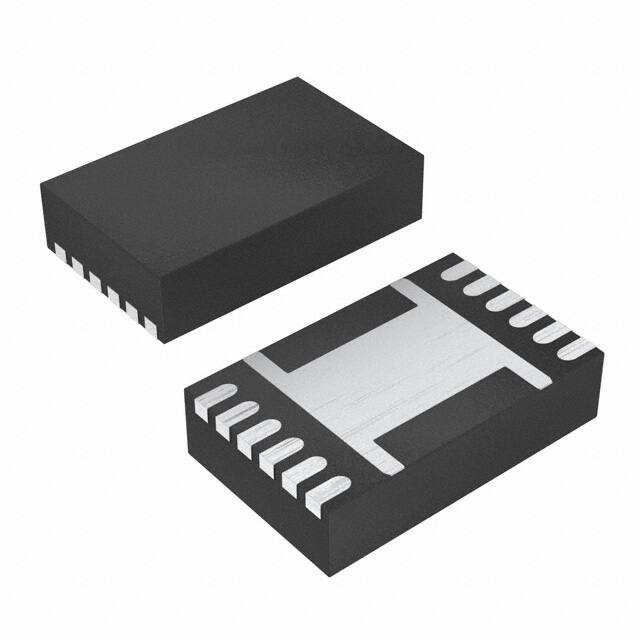
Compact 12-pin VSON package (DRZ)
The BQ28Z610-R1 device provides a fully integrated
pack-based solution with a flash programmable
custom reduced instruction-set CPU (RISC), safety
protection, and authentication for 1- to 2-series cell
Li-Ion and Li-Polymer battery packs.
The BQ28Z610-R1 gas gauge communicates via an
I2C compatible interface and combines an ultra-lowpower, high-speed TI BQBMP processor, highaccuracy analog measurement capabilities, integrated
flash memory, an array of peripheral and
communication ports, an N-CH FET drive, and a
SHA-1 Authentication transform responder into a
complete, high-performance battery management
solution.
Device Information(1)
PART NUMBER
2 Applications
•
•
•
The BQ28Z610-R1 device enables autonomous
charge control through Master Mode I2C broadcasts
of charging current and voltage information,
eliminating software overhead that is typically
incurred by the system's host controller.
BQ28Z610-R1
Tablet computing
Portable and wearable health devices
Portable audio devices
– Wireless (bluetooth) speakers
PACKAGE
BODY SIZE (NOM)
VSON (12)
4 mm × 2.5 mm
(1) For all available packages, see the orderable addendum at
the end of the data sheet.
Simplified Schematic
Wireless (Bluetooth) Speaker Application
Block Diagram
Pack+
10 M
10 M
Fuse
13
1
VSS
PWPD
2s
0.1 µF
2
SRN
VC2 11
3
SRP
PBI 10
4
TS1
100
Comm
Bus
1 µF
1s
5
0.1 µF
5.1 k
Gauge
2.2 µF
5
SCL
PACK 8
6
SDA
DSG 7
100
Audio Processor
I2C
System Side
Power
100
1 to 10 mΩ
MCU
Pack Side
100
MM3Z5V6C
Pack–
Battery
cells
10
100
MM3Z5V6C
100
Charger
5.1 k
CHG 9
10k
Audio
Power Amp
Boost Converter
Battery
100
VC1 12
Copyright © 2017, Texas Instruments Incorporated
Copyright © 2016, Texas Instruments Incorporated
1
An IMPORTANT NOTICE at the end of this data sheet addresses availability, warranty, changes, use in safety-critical applications,
intellectual property matters and other important disclaimers. PRODUCTION DATA.
�BQ28Z610-R1
SLUSE07A – JANUARY 2020 – REVISED FEBRUARY 2020
www.ti.com
Table of Contents
1
2
3
4
5
6
7
Features ..................................................................
Applications ...........................................................
Description .............................................................
Revision History.....................................................
Description (continued).........................................
Pin Configuration and Functions .........................
Specifications.........................................................
1
1
1
2
2
3
4
7.1
7.2
7.3
7.4
7.5
7.6
7.7
7.8
7.9
7.10
7.11
7.12
7.13
7.14
7.15
7.16
7.17
7.18
7.19
7.20
7.21
4
4
4
5
5
5
5
6
6
6
6
7
7
7
8
8
8
8
8
9
9
Absolute Maximum Ratings ......................................
ESD Ratings ............................................................
Recommended Operating Conditions.......................
Thermal Information ..................................................
Supply Current ..........................................................
Power Supply Control ...............................................
Low-Voltage General Purpose I/O, TS1 ...................
Power-On Reset (POR) ............................................
Internal 1.8-V LDO ....................................................
Current Wake Comparator......................................
Coulomb Counter ....................................................
ADC Digital Filter ....................................................
ADC Multiplexer ......................................................
Cell Balancing Support ...........................................
Internal Temperature Sensor ..................................
NTC Thermistor Measurement Support..................
High-Frequency Oscillator.......................................
Low-Frequency Oscillator .......................................
Voltage Reference 1 ...............................................
Voltage Reference 2 ...............................................
Instruction Flash......................................................
7.22
7.23
7.24
7.25
7.26
7.27
7.28
8
Detailed Description ............................................ 16
8.1
8.2
8.3
8.4
9
Data Flash............................................................... 9
Current Protection Thresholds ................................ 9
Current Protection Timing ..................................... 10
N-CH FET Drive (CHG, DSG)............................... 11
I2C Interface I/O .................................................... 11
I2C Interface Timing .............................................. 11
Typical Characteristics ......................................... 13
Overview .................................................................
Functional Block Diagram .......................................
Feature Description.................................................
Device Functional Modes........................................
16
16
17
21
Applications and Implementation ...................... 23
9.1 Application Information............................................ 23
9.2 Typical Applications ............................................... 23
10 Power Supply Recommendations ..................... 26
11 Layout................................................................... 26
11.1 Layout Guidelines ................................................. 26
11.2 Layout Example .................................................... 28
12 Device and Documentation Support ................. 29
12.1
12.2
12.3
12.4
12.5
12.6
Documentation Support ........................................
Receive Documentation Update Notifications.......
Support Resources ...............................................
Trademarks ...........................................................
Electrostatic Discharge Caution ............................
Glossary ................................................................
29
29
29
29
29
29
13 Mechanical, Packaging, and Orderable
Information ........................................................... 29
4 Revision History
Changes from Original (February 2020) to Revision A
•
Page
Changed I2C Interface I/O ................................................................................................................................................... 11
5 Description (continued)
The BQ28Z610-R1 device provides an array of battery and system safety functions, including overcurrent in
discharge, short circuit in charge, and short circuit in discharge protection for the battery, as well as FET
protection for the N-channel FETs, internal AFE watchdog, and cell balancing. Through firmware, the devices
can provide a larger array of features including protection against overvoltage, undervoltage, overtemperature,
and more.
2
Submit Documentation Feedback
Copyright © 2020, Texas Instruments Incorporated
Product Folder Links: BQ28Z610-R1
�BQ28Z610-R1
www.ti.com
SLUSE07A – JANUARY 2020 – REVISED FEBRUARY 2020
6 Pin Configuration and Functions
DRZ Package
12-Pin VSON
Top View
VSS
1
12
VC1
SRN
2
11
VC2
SRP
3
10
PBI
TS1
4
SCL
SDA
Thermal
Pad
9
CHG
5
8
PACK
6
7
DSG
Not to scale
Pin Functions
PIN
NUMBER
PIN NAME
TYPE
1
VSS
P (1)
2
SRN
AI
Analog input pin connected to the internal coulomb counter peripheral for integrating a
small voltage between SRP and SRN where SRP is the top of the sense resistor.
3
SRP
AI
Analog input pin connected to the internal coulomb counter peripheral for integrating a
small voltage between SRP and SRN where SRP is the top of the sense resistor.
4
TS1
AI
Temperature input for ADC to the oversampled ADC channel, and optional Battery Trip
Point (BTP) output
5
SCL
I/O
Serial Clock for I2C interface; requires external pullup when used
6
SDA
I/O
Serial Data for I2C interface; requires external pullup
N-CH FET drive output pin
7
DSG
O
8
PACK
AI, P
Device ground
Pack sense input pin
9
CHG
O
N-CH FET drive output pin
10
PBI
P
Power supply backup input pin
11
VC2
AI, P
Sense voltage input pin for most positive cell, balance current input for most positive cell.
Primary power supply input and battery stack measurement input (BAT)
VC1
AI
Sense voltage input pin for least positive cell, balance current input for least positive cell
PWPD
—
Exposed Pad, electrically connected to VSS (external trace)
12
(1)
DESCRIPTION
P = Power Connection, O = Digital Output, AI = Analog Input, I = Digital Input, I/O = Digital Input/Output
Submit Documentation Feedback
Copyright © 2020, Texas Instruments Incorporated
Product Folder Links: BQ28Z610-R1
3
�BQ28Z610-R1
SLUSE07A – JANUARY 2020 – REVISED FEBRUARY 2020
www.ti.com
7 Specifications
7.1 Absolute Maximum Ratings
Over operating free-air temperature range (unless otherwise noted) (1)
Supply voltage range, VCC
MIN
MAX
UNIT
VC2, PBI
–0.3
30
V
PACK
–0.3
30
V
TS
–0.3
VREG + 0.3
V
SRP, SRN
–0.3
0.3
V
VC2
VC1 – 0.3
VC1 + 8.5 or
VSS + 30
V
VC1
VSS – 0.3
VSS + 8.5 or
VSS + 30
V
V
Input voltage range, VIN
Communication Interface
SDA, SCL
–0.3
6
Output voltage range, VO
CHG, DSG
–0.3
32
V
±50
mA
Maximum VSS current, ISS
Functional Temperature, TFUNC
–40
Lead temperature (soldering, 10 s), TSOLDER
Storage temperature range, TSTG
(1)
–65
110
°C
±300
°C
150
°C
Stresses beyond those listed under absolute maximum ratings may cause permanent damage to the device. These are stress ratings
only, and functional operation of the device at these or any other conditions beyond those indicated under recommended operating
conditions is not implied. Exposure to absolute–maximum–rated conditions for extended periods may affect device reliability.
7.2 ESD Ratings
VALUE
V(ESD)
(1)
(2)
Human body model (HBM), per ANSI/ESDA/JEDEC JS-001, all pins (1)
±2000
Charged device model (CDM), per JEDEC specification JESD22-C101, all
pins (2)
±500
UNIT
V
JEDEC document JEP155 states that 500-V HBM allows safe manufacturing with a standard ESD control process.
JEDEC document JEP157 states that 250-V CDM allows safe manufacturing with a standard ESD control process.
7.3 Recommended Operating Conditions
Typical values stated where TA = 25ºC and VCC = 7.2 V, Min/Max values stated where TA = –40ºC to 85ºC and VCC = 2.2 V
to 26 V (unless otherwise noted)
PARAMETER
TEST CONDITION
MIN
VCC
Supply voltage
VC2, PBI
2.2
VSHUTDOWN–
Shutdown voltage
VPACK < VSHUTDOWN–
1.8
VSHUTDOWN+
Start-up voltage
VPACK > VSHUTDOWN– + VHYS
2.05
VHYS
Shutdown voltage
hysteresis
VSHUTDOWN+ – VSHUTDOWN–
V
2.0
2.2
V
2.25
2.45
V
mV
VREG
SRP, SRN
–0.2
0.2
VC2
VVC1
VVC1 + 5
VC1
VVSS
VVSS + 5
PACK
V
26
VO
Output voltage range
CPBI
External PBI capacitor
2.2
TOPR
Operating temperature
–40
4
UNIT
26
5.5
TS1
Input voltage range
MAX
250
SDA, SCL
VIN
NOM
CHG, DSG
Submit Documentation Feedback
26
V
µF
85
°C
Copyright © 2020, Texas Instruments Incorporated
Product Folder Links: BQ28Z610-R1
�BQ28Z610-R1
www.ti.com
SLUSE07A – JANUARY 2020 – REVISED FEBRUARY 2020
7.4 Thermal Information
BQ28Z610-R1
THERMAL METRIC (1)
DRZ
UNIT
12 PINS
RθJA, High K
Junction-to-ambient thermal resistance
RθJC(top)
Junction-to-case(top) thermal resistance
90.4
RθJB
Junction-to-board thermal resistance
110.7
ψJT
Junction-to-top characterization parameter
96.7
ψJB
Junction-to-board characterization parameter
90
RθJC(bottom)
Junction-to-case(bottom) thermal resistance
n/a
(1)
186.4
°C/W
For more information about traditional and new thermal metrics, see the Semiconductor and IC Package Thermal Metrics application
report, SPRA953.
7.5 Supply Current
Typical values stated where TA = 25ºC and VCC = 7.2 V, Min/Max values stated where TA = –40ºC to 85ºC and VCC = 2.2 V
to 7.6 V (unless otherwise noted)
PARAMETER
INORMAL (1)
TEST CONDITION
MIN
TYP
NORMAL mode
CHG = ON, DSG = ON, No Flash Write
250
ISLEEP (1)
SLEEP mode
CHG = OFF, DSG = OFF, No Communication on
Bus
100
ISHUTDOWN
SHUTDOWN mode
(1)
0.5
MAX
UNIT
µA
2
µA
Dependent on the use of the correct firmware (FW) configuration
7.6 Power Supply Control
Typical values stated where TA = 25ºC and VCC = 7.2 V, Min/Max values stated where TA = –40ºC to 85ºC and VCC = 2.2 V
to 7.6 V (unless otherwise noted)
PARAMETER
MIN
TYP
MAX
VVC2 < VSWITCHOVER–
2.0
2.1
2.2
V
PACK to VC2
switchover voltage
VVC2 > VSWITCHOVER– + VHYS
3.0
3.1
3.2
V
Switchover voltage
hysteresis
VSWITCHOVER+ – VSWITCHOVER–
VSWITCHOVER–
VC2 to PACK
switchover voltage
VSWITCHOVER+
VHYS
ILKG
RPACK(PD)
Input Leakage
current
Internal pulldown
resistance
TEST CONDITION
1000
mV
VC2 pin, VC2 = 0 V, PACK = 25 V
1
PACK pin, VC2 = 25 V, PACK = 0 V
1
VC2 and PACK pins, VC2 = 0 V, PACK = 0 V,
PBI = 25 V
1
PACK
30
40
UNIT
50
µA
kΩ
7.7 Low-Voltage General Purpose I/O, TS1
Typical values stated where TA = 25ºC and VCC = 7.2 V, Min/Max values stated where TA = –40ºC to 85ºC and VCC = 2.2 V
to 7.6 V (unless otherwise noted)
PARAMETER
TEST CONDITION
VIH
High-level input
VIL
Low-level input
VOH
Output voltage high
IOH = –1.0 mA
VOL
Output voltage low
IOL = 1.0 mA
CIN
Input capacitance
ILKG
Input leakage
current
MIN
TYP
MAX
0.65 x VREG
V
0.35 x VREG
0.75 x VREG
5
V
pF
1
Submit Documentation Feedback
Product Folder Links: BQ28Z610-R1
V
V
0.2 x VREG
Copyright © 2020, Texas Instruments Incorporated
UNIT
µA
5
�BQ28Z610-R1
SLUSE07A – JANUARY 2020 – REVISED FEBRUARY 2020
www.ti.com
7.8 Power-On Reset (POR)
Typical values stated where TA = 25ºC and VCC = 7.2 V, Min/Max values stated where TA = –40ºC to 85ºC and VCC = 2.2 V
to 7.6 V (unless otherwise noted)
PARAMETER
TEST CONDITION
VREGIT–
Negative-going voltage
input
VREG
VHYS
Power-on reset
hysteresis
VREGIT+ – VREGIT–
tRST
Power-on reset time
MIN
TYP
MAX
UNIT
1.51
1.55
1.59
V
70
100
130
mV
200
300
400
µs
7.9 Internal 1.8-V LDO
Typical values stated where TA = 25ºC and VCC = 7.2 V, Min/Max values stated where TA = –40ºC to 85ºC and VCC = 2.2 V
to 7.6 V (unless otherwise noted)
PARAMETER
TEST CONDITION
MIN
TYP
MAX
1.6
1.8
2.0
VREG
Regulator voltage
ΔVO(TEMP)
Regulator output over
temperature
ΔVREG/ΔTA, IREG = 10 mA
ΔVO(LINE)
Line regulation
ΔVREG/ΔVBAT, VBAT = 10 mA
–0 .6%
0.5%
ΔVO(LOAD)
Load regulation
ΔVREG/ΔIREG, IREG = 0 mA to 10 mA
–1.5%
1.5%
IREG
Regulator output
current limit
VREG = 0.9 x VREG(NOM), VIN > 2.2 V
20
ISC
Regulator short-circuit
current limit
VREG = 0 x VREG(NOM)
25
PSRRREG
Power supply rejection
ratio
ΔVBAT/ΔVREG, IREG = 10 mA, VIN > 2.5 V, f = 10 Hz
VSLEW
Slew rate enhancement
VREG
voltage threshold
UNIT
V
±0.25%
1.58
mA
40
50
mA
40
dB
1.65
V
7.10 Current Wake Comparator
Typical values stated where TA = 25ºC and VCC = 7.2 V, Min/Max values stated where TA = –40ºC to 85ºC and VCC = 2.2 V
to 7.6 V (unless otherwise noted)
PARAMETER
Wake voltage
threshold
VWAKE
VWAKE(DRIFT)
Temperature drift of
VWAKE accuracy
tWAKE
Time from application
of current to wake
tWAKE(SU)
Wake up comparator
startup time
TEST CONDITION
MIN
TYP
MAX
UNIT
VWAKE = VSRP – VSRN WAKE_CONTROL[WK1, WK0]
= 0,0
±0.3
±0.625
±0.9
mV
VWAKE = VSRP – VSRN WAKE_CONTROL[WK1, WK0]
= 0,1
±0.6
±1.25
±1.8
mV
VWAKE = VSRP – VSRN WAKE_CONTROL[WK1, WK0]
= 1,0
±1.2
±2.5
±3.6
mV
VWAKE = VSRP – VSRN WAKE_CONTROL[WK1, WK0]
= 1,1
±2.4
±5.0
±7.2
mV
0.5%
[WKCHGEN] = 0 and [WKDSGEN] = 0 to
[WKCHGEN] = 1 and [WKDSGEN] = 1
°C
0.25
0.5
ms
250
640
µs
7.11 Coulomb Counter
Typical values stated where TA = 25ºC and VCC = 7.2 V, Min/Max values stated where TA = –40ºC to 85ºC and VCC = 2.2 V
to 7.6 V (unless otherwise noted)
PARAMETER
TEST CONDITION
Input voltage range
Full scale range
Differential nonlinearity
6
16-bit, no missing codes
Submit Documentation Feedback
MAX
UNIT
–100
MIN
TYP
100
mV
–VREF1/10
+VREF1/10
mV
±1
LSB
Copyright © 2020, Texas Instruments Incorporated
Product Folder Links: BQ28Z610-R1
�BQ28Z610-R1
www.ti.com
SLUSE07A – JANUARY 2020 – REVISED FEBRUARY 2020
Coulomb Counter (continued)
Typical values stated where TA = 25ºC and VCC = 7.2 V, Min/Max values stated where TA = –40ºC to 85ºC and VCC = 2.2 V
to 7.6 V (unless otherwise noted)
PARAMETER
TEST CONDITION
TYP
MAX
UNIT
±5.2
±22.3
LSB
16-bit, post-calibration
±1.3
±2.6
LSB
15-bit + sign, post-calibration
0.04
0.07
LSB/°C
Gain error
15-bit + sign, over input voltage range
±131
±492
LSB
Gain error drift
15-bit + sign, over input voltage range
4.3
9.8
Integral nonlinearity
16-bit, best fit over input voltage range
Offset error
Offset error drift
Effective input resistance
MIN
LSB/°C
2.5
MΩ
7.12 ADC Digital Filter
Typical values stated where TA = 25ºC and VCC = 7.2 V, Min/Max values stated where TA = –40ºC to 85ºC and VCC = 2.2 V
to 7.6 V (unless otherwise noted)
PARAMETER
tCONV
TEST CONDITION
MIN
31.25
ADCTL[SPEED1, SPEED0] = 0, 1
15.63
ADCTL[SPEED1, SPEED0] = 1, 0
7.81
ADCTL[SPEED1, SPEED0] = 1, 1
1.95
No missing codes, ADCTL[SPEED1, SPEED0] =
0, 0
Resolution
Effective resolution
TYP
ADCTL[SPEED1, SPEED0] = 0, 0
MAX
ms
16
With sign, ADCTL[SPEED1, SPEED0] = 0, 0
14
15
With sign, ADCTL[SPEED1, SPEED0] = 0, 1
13
14
With sign, ADCTL[SPEED1, SPEED0] = 1, 0
11
12
With sign, ADCTL[SPEED1, SPEED0] = 1, 1
9
10
UNIT
Bits
Bits
7.13 ADC Multiplexer
Typical values stated where TA = 25ºC and VCC = 7.2 V, Min/Max values stated where TA = –40ºC to 85ºC and VCC = 2.2 V
to 7.6 V (unless otherwise noted)
PARAMETER
K
Scaling factor
TEST CONDITION
MIN
TYP
MAX
VC1–VSS, VC2–VC1
0.1980
0.2000
0.2020
VC2–VSS, PACK–VSS
0.0485
0.050
0.051
0.490
0.500
0.510
VREF1/2
VIN
ILKG
Input voltage range
Input leakage current
VC2–VSS, PACK–VSS
–0.2
20
TS1
–0.2
0.8 × VREF1
TS1
–0.2
0.8 × VREG
VC1, VC2 cell balancing off, cell detach detection
off, ADC multiplexer off
1
UNIT
—
V
µA
7.14 Cell Balancing Support
Typical values stated where TA = 25ºC and VCC = 7.2 V, Min/Max values stated where TA = –40ºC to 85ºC and VCC = 2.2 V
to 7.6 V (unless otherwise noted)
PARAMETER
RCB
Internal cell balance
resistance
TEST CONDITION
RDS(ON) for internal FET switch at 2 V < VDS < 4 V
MIN
TYP
MAX
UNIT
200
Ω
Submit Documentation Feedback
Copyright © 2020, Texas Instruments Incorporated
Product Folder Links: BQ28Z610-R1
7
�BQ28Z610-R1
SLUSE07A – JANUARY 2020 – REVISED FEBRUARY 2020
www.ti.com
7.15 Internal Temperature Sensor
Typical values stated where TA = 25ºC and VCC = 7.2 V, Min/Max values stated where TA = –40ºC to 85ºC and VCC = 2.2 V
to 7.6 V (unless otherwise noted)
PARAMETER
Internal temperature
sensor voltage drift
VTEMP
(1)
TEST CONDITION
VTEMPP
VTEMPP – VTEMPN
(1)
MIN
TYP
MAX
–1.9
–2.0
–2.1
0.177
0.178
0.179
UNIT
mV/°C
Assured by design
7.16 NTC Thermistor Measurement Support
Typical values stated where TA = 25ºC and VCC = 7.2 V, Min/Max values stated where TA = –40ºC to 85ºC and VCC = 2.2 V
to 7.6 V (unless otherwise noted)
PARAMETER
RNTC(PU)
Internal pull-up
resistance
RNTC(DRIFT)
Resistance drift over
temperature
TEST CONDITION
MIN
TYP
MAX
UNIT
TS1
14.4
18
21.6
kΩ
TS1
–360
–280
–200
PPM/°C
7.17 High-Frequency Oscillator
Typical values stated where TA = 25ºC and VCC = 7.2 V, Min/Max values stated where TA = –40ºC to 85ºC and VCC = 2.2 V
to 7.6 V (unless otherwise noted)
PARAMETER
fHFO
TEST CONDITION
MIN
Operating frequency
fHFO(ERR)
Frequency error
tHFO(SU)
Start-up time
TYP
MAX
16.78
MHz
TA = –20°C to 70°C, includes frequency drift
–2.5%
±0.25%
2.5%
TA = –40°C to 85°C, includes frequency drift
–3.5%
±0.25%
3.5%
TA = –20°C to 85°C, Oscillator frequency within
+/–3% of nominal, CLKCTL[HFRAMP] = 1
Oscillator frequency within +/–3% of nominal,
CLKCTL[HFRAMP] = 0
UNIT
4
ms
100
µs
7.18 Low-Frequency Oscillator
Typical values stated where TA = 25ºC and VCC = 7.2 V, Min/Max values stated where TA = –40ºC to 85ºC and VCC = 2.2 V
to 7.6 V (unless otherwise noted)
PARAMETER
fLFO
Operating frequency
fLFO(LP)
Operating frequency in
low power mode
fLFO(ERR)
Frequency error
fLFO(LPERR)
Frequency error in low
power mode
fLFO(FAIL)
Failure detection
frequency
TEST CONDITION
MIN
TYP
MAX
kHz
247
kHz
TA = –20°C to 70°C, includes frequency drift
–1.5%
±0.25%
1.5%
TA = –40°C to 85°C, includes frequency drift
–2.5%
±0.25%
2.5%
–5%
30
UNIT
262.144
5%
80
100
kHz
7.19 Voltage Reference 1
Typical values stated where TA = 25ºC and VCC = 7.2 V, Min/Max values stated where TA = –40ºC to 85ºC and VCC = 2.2 V
to 7.6 V (unless otherwise noted)
PARAMETER
VREF1
Internal reference
voltage
VREF1(DRIFT)
Internal reference
voltage drift
8
TEST CONDITION
TA = 25°C, after trim
MIN
TYP
MAX
UNIT
1.215
1.220
1.225
V
TA = 0°C to 60°C, after trim
±50
TA = –40°C to 85°C, after trim
±80
Submit Documentation Feedback
PPM/°C
Copyright © 2020, Texas Instruments Incorporated
Product Folder Links: BQ28Z610-R1
�BQ28Z610-R1
www.ti.com
SLUSE07A – JANUARY 2020 – REVISED FEBRUARY 2020
7.20 Voltage Reference 2
Typical values stated where TA = 25ºC and VCC = 7.2 V, Min/Max values stated where TA = –40ºC to 85ºC and VCC = 2.2 V
to 7.6 V (unless otherwise noted)
PARAMETER
VREF2
Internal reference
voltage
VREF2(DRIFT)
Internal reference
voltage drift
TEST CONDITION
TA = 25°C, after trim
MIN
TYP
MAX
UNIT
1.215
1.220
1.225
V
TA = 0°C to 60°C, after trim
±50
TA = –40°C to 85°C, after trim
±80
PPM/°C
7.21 Instruction Flash
Typical values stated where TA = 25ºC and VCC = 7.2 V, Min/Max values stated where TA = –40ºC to 85ºC and VCC = 2.2 V
to 7.6 V (unless otherwise noted)
PARAMETER
TEST CONDITION
Data retention
Flash programming
write cycles
MIN
TYP
MAX
UNIT
10
Years
1000
Cycles
tPROGWORD
Word programming
time
TA = –40°C to 85°C
40
µs
tMASSERASE
Mass-erase time
TA = –40°C to 85°C
40
ms
tPAGEERASE
Page-erase time
TA = –40°C to 85°C
40
ms
IFLASHREAD
Flash-read current
TA = –40°C to 85°C
2
mA
IFLASHWRITE
Flash-write current
TA = –40°C to 85°C
5
mA
IFLASHERASE
Flash-erase current
TA = –40°C to 85°C
15
mA
7.22 Data Flash
Typical values stated where TA = 25ºC and VCC = 7.2 V, Min/Max values stated where TA = –40ºC to 85ºC and VCC = 2.2 V
to 7.6 V (unless otherwise noted)
PARAMETER
TEST CONDITION
Data retention
Flash programming
write cycles
MIN
TYP
MAX
UNIT
10
Years
20000
Cycles
tPROGWORD
Word programming
time
TA = –40°C to 85°C
40
µs
tMASSERASE
Mass-erase time
TA = –40°C to 85°C
40
ms
tPAGEERASE
Page-erase time
TA = –40°C to 85°C
40
ms
IFLASHREAD
Flash-read current
TA = –40°C to 85°C
1
mA
IFLASHWRITE
Flash-write current
TA = –40°C to 85°C
5
mA
IFLASHERASE
Flash-erase current
TA = –40°C to 85°C
15
mA
7.23 Current Protection Thresholds
Typical values stated where TA = 25ºC and VCC = 7.2 V, Min/Max values stated where TA = –40ºC to 85ºC and VCC = 2.2 V
to 7.6 V (unless otherwise noted)
PARAMETER
VOCD
ΔVOCD
OCD detection threshold
voltage range
OCD detection threshold
voltage program step
TEST CONDITION
MIN
TYP
MAX
VOCD = VSRP – VSRN,
PROTECTION_CONTROL[RSNS] = 1
–16.6
–100
VOCD = VSRP – VSRN,
PROTECTION_CONTROL[RSNS] = 0
–8.3
–50
mV
VOCD = VSRP – VSRN,
PROTECTION_CONTROL[RSNS] = 1
–5.56
VOCD = VSRP – VSRN,
PROTECTION_CONTROL[RSNS] = 0
–2.78
mV
Submit Documentation Feedback
Copyright © 2020, Texas Instruments Incorporated
Product Folder Links: BQ28Z610-R1
UNIT
9
�BQ28Z610-R1
SLUSE07A – JANUARY 2020 – REVISED FEBRUARY 2020
www.ti.com
Current Protection Thresholds (continued)
Typical values stated where TA = 25ºC and VCC = 7.2 V, Min/Max values stated where TA = –40ºC to 85ºC and VCC = 2.2 V
to 7.6 V (unless otherwise noted)
PARAMETER
ΔVSCC
ΔVSCC
VSCD1
ΔVSCD1
VSCD2
ΔVSCD2
TEST CONDITION
SCC detection threshold
voltage range
SCC detection threshold
voltage program step
SCD1 detection threshold
voltage range
SCD1 detection threshold
voltage program step
SCD2 detection threshold
voltage range
SCD2 detection threshold
voltage program step
MIN
TYP
MAX
VSCC = VSRP – VSRN,
PROTECTION_CONTROL[RSNS] = 1
44.4
200
VSCC = VSRP – VSRN,
PROTECTION_CONTROL[RSNS] = 0
22.2
100
UNIT
mV
VSCC = VSRP – VSRN,
PROTECTION_CONTROL[RSNS] = 1
22.2
VSCC = VSRP – VSRN,
PROTECTION_CONTROL[RSNS] = 0
11.1
mV
VSCD1 = VSRP – VSRN,
PROTECTION_CONTROL[RSNS] = 1
–44.4
–200
VSCD1 = VSRP – VSRN,
PROTECTION_CONTROL[RSNS] = 0
–22.2
–100
mV
VSCD1 = VSRP – VSRN,
PROTECTION_CONTROL[RSNS] = 1
–22.2
VSCD1 = VSRP – VSRN,
PROTECTION_CONTROL[RSNS] = 0
–11.1
mV
VSCD2 = VSRP – VSRN,
PROTECTION_CONTROL[RSNS] = 1
–44.4
–200
VSCD2 = VSRP – VSRN,
PROTECTION_CONTROL[RSNS] = 0
–22.2
–100
mV
VSCD2 = VSRP – VSRN,
PROTECTION_CONTROL[RSNS] = 1
–22.2
VSCD2 = VSRP – VSRN,
PROTECTION_CONTROL[RSNS] = 0
–11.1
mV
7.24 Current Protection Timing
Typical values stated where TA = 25ºC and VCC = 7.2 V, Min/Max values stated where TA = –40ºC to 85ºC and VCC = 2.2 V
to 7.6 V (unless otherwise noted)
PARAMETER
TEST CONDITION
MIN
NOM
MAX
tOCD
OCD detection delay
time
ΔtOCD
OCD detection delay
time program step
tSCC
SCC detection delay
time
ΔtSCC
SCC detection delay
time program step
tSCD1
SCD1 detection delay
time
PROTECTION_CONTROL[SCDDx2] = 0
0
915
PROTECTION_CONTROL[SCDDx2] = 1
0
1850
ΔtSCD1
SCD1 detection delay
time program step
PROTECTION_CONTROL[SCDDx2] = 0
61
PROTECTION_CONTROL[SCDDx2] = 1
121
tSCD2
SCD2 detection delay
time
PROTECTION_CONTROL[SCDDx2] = 0
0
458
PROTECTION_CONTROL[SCDDx2] = 1
0
915
ΔtSCD2
SCD2 detection delay
time program step
PROTECTION_CONTROL[SCDDx2] = 0
30.5
PROTECTION_CONTROL[SCDDx2] = 1
61
tDETECT
Current fault detect
time
VSRP – VSRN = VT – 3 mV for OCD, SCD1, and SC2,
VSRP – VSRN = VT + 3 mV for SCC
tACC
Current fault delay time
Max delay setting
accuracy
10
1
31
2
0
Submit Documentation Feedback
ms
ms
915
61
µs
µs
µs
µs
µs
µs
160
–10%
UNIT
µs
10%
Copyright © 2020, Texas Instruments Incorporated
Product Folder Links: BQ28Z610-R1
�BQ28Z610-R1
www.ti.com
SLUSE07A – JANUARY 2020 – REVISED FEBRUARY 2020
7.25 N-CH FET Drive (CHG, DSG)
Typical values stated where TA = 25ºC and VCC = 7.2 V, Min/Max values stated where TA = –40ºC to 85ºC and VCC = 2.2 V
to 7.6 V (unless otherwise noted)
PARAMETER
Output voltage ratio
V(FETON)
V(FETOFF)
tR
tF
Output voltage,
CHG and DSG on
Output voltage,
CHG and DSG off
Rise time
Fall time
MIN
TYP
MAX
RatioDSG = (VDSG – VVC2)/VVC2, 2.2 V < VVC2 < 4.07 V, 10
MΩ between PACK and DSG
TEST CONDITION
2.133
2.333
2.467
RatioCHG = (VCHG – VVC2)/VVC2, 2.2 V < VVC2 < 4.07 V, 10
MΩ between BAT and CHG
2.133
2.333
2.467
VDSG(ON) = VDSG – VVC2, 4.07 V ≤ VVC2 ≤ 18 V, 10 MΩ
between PACK and DSG
8.75
9.5
10.25
VCHG(ON) = VCHG – VVC2, 4.07 V ≤ VVC2 ≤ 18 V, 10 MΩ
between VC2 and CHG
8.75
9.5
10.25
VDSG(OFF) = VDSG – VPACK, 10 MΩ between PACK and
DSG
–0.4
0.4
VCHG(OFF) = VCHG – VBAT, 10 MΩ between VC2 and CHG
–0.4
0.4
UNIT
—
V
VDSG from 0% to 35% VDSG(ON)(TYP), VBAT ≥ 2.2 V, CL =
4.7 nF between DSG and PACK, 5.1 kΩ between DSG
and CL, 10 MΩ between PACK and DSG
200
VCHG from 0% to 35% VCHG(ON)(TYP), VVC2 ≥ 2.2 V, CL =
4.7 nF between CHG and VC2, 5.1 kΩ between CHG and
CL, 10 MΩ between VC2 and CHG
200
500
VDSG from VDSG(ON)(TYP) to 1 V, VVC2 ≥ 2.2 V, CL = 4.7 nF
between DSG and PACK, 5.1 kΩ between DSG and CL,
10 MΩ between PACK and DSG
40
300
VCHG from VCHG(ON)(TYP) to 1 V, VVC2 ≥ 2.2 V, CL = 4.7 nF
between CHG and VC2, 5.1 kΩ between CHG and CL, 10
MΩ between VC2 and CHG
40
V
500
µs
µs
200
7.26 I2C Interface I/O
Typical values stated where TA = 25ºC and VCC = 7.2 V, Min/Max values stated where TA = –40ºC to 85ºC and VCC = 2.2 V
to 7.6 V (unless otherwise noted)
PARAMETER
TEST CONDITION
MIN
VIH
Input voltage high
SCL, SDA (STANDARD and FAST modes)
0.7 × VREG
VIL
Input voltage low
SCL, SDA (STANDARD and FAST modes)
–0.5
VOL
Output low voltage
SCL, SDA, IOL = 1 mA (STANDARD and FAST modes)
CIN
Input capacitance
ILKG
Input leakage
current
RPD
Pull-down resistance
TYP
MAX
UNIT
V
0.3 × VREG
V
0.2 × VREG
V
10
pF
1
µA
3.3
kΩ
7.27 I2C Interface Timing
Typical values stated where TA = 25ºC and VCC = 7.2 V, Min/Max values stated where TA = –40ºC to 85ºC and VCC = 2.2 V
to 7.6 V (unless otherwise noted)
PARAMETER
TEST CONDITION
MIN
NOM
MAX
UNIT
300
ns
300
ns
tR
Clock rise time
10% to 90%
tF
Clock fall time
90% to 10%
tHIGH
Clock high period
600
ns
tLOW
Clock low period
1.3
µs
tSU(START)
Repeated start setup
time
600
ns
td(START)
Start for first falling
edge to SCL
600
ns
tSU(DATA)
Data setup time
100
ns
tHD(DATA)
Data hold time
0
µs
tSU(STOP)
Stop setup time
600
ns
Submit Documentation Feedback
Copyright © 2020, Texas Instruments Incorporated
Product Folder Links: BQ28Z610-R1
11
�BQ28Z610-R1
SLUSE07A – JANUARY 2020 – REVISED FEBRUARY 2020
www.ti.com
I2C Interface Timing (continued)
Typical values stated where TA = 25ºC and VCC = 7.2 V, Min/Max values stated where TA = –40ºC to 85ºC and VCC = 2.2 V
to 7.6 V (unless otherwise noted)
PARAMETER
TEST CONDITION
tBUF
Bus free time
between stop and
start
fSW
Clock operating
frequency
MIN
NOM
MAX
1.3
µs
SLAVE mode, SCL 50% duty cycle
tSU(STA)
tw(H)
400
tf
tw(L)
UNIT
tr
kHz
t(BUF)
SCL
SDA
td(STA)
tf
tr
th(DAT)
tsu(STOP)
tsu(DAT)
REPEATED
START
STOP
START
Figure 1. I2C Timing
12
Submit Documentation Feedback
Copyright © 2020, Texas Instruments Incorporated
Product Folder Links: BQ28Z610-R1
�BQ28Z610-R1
www.ti.com
SLUSE07A – JANUARY 2020 – REVISED FEBRUARY 2020
7.28 Typical Characteristics
0.15
8.0
Max CC Offset Error
Min CC Offset Error
6.0
ADC Offset Error (µV)
CC Offset Error ( V)
0.10
0.05
0.00
±0.05
±0.10
4.0
2.0
0.0
±2.0
±4.0
±6.0
±0.15
Max ADC Offset Error
Min ADC Offset Error
±8.0
±40
±20
0
20
40
60
80
100
Temperature (ƒC)
120
±40
Figure 2. CC Offset Error vs. Temperature
20
40
60
80
100
120
C003
Figure 3. ADC Offset Error vs. Temperature
264
Low-Frequency Oscillator (kHz)
Reference Voltage (V)
0
Temperature (°C)
1.24
1.23
1.22
1.21
1.20
262
260
258
256
254
252
250
±40
0
±20
20
40
60
80
Temperature (ƒC)
100
±40
0
±20
20
40
60
80
Temperature (ƒC)
C006
Figure 4. Reference Voltage vs. Temperature
100
C007
Figure 5. Low-Frequency Oscillator vs. Temperature
16.9
±24.6
OCD Protection Threshold (mV)
High-Frequency Oscillator (MHz)
±20
C001
16.8
16.7
16.6
±24.8
±25.0
±25.2
±25.4
±25.6
±25.8
±40
±20
0
20
40
60
Temperature (ƒC)
80
100
120
±40
±20
0
20
40
60
80
100
Temperature (ƒC)
C008
120
C009
Threshold setting is 25 mV.
Figure 6. High-Frequency Oscillator vs. Temperature
Figure 7. Overcurrent Discharge Protection Threshold vs.
Temperature
Submit Documentation Feedback
Copyright © 2020, Texas Instruments Incorporated
Product Folder Links: BQ28Z610-R1
13
�BQ28Z610-R1
SLUSE07A – JANUARY 2020 – REVISED FEBRUARY 2020
www.ti.com
Typical Characteristics (continued)
±86.0
SCD 1 Protection Threshold (mV)
SCC Protection Threshold (mV)
87.4
87.2
87.0
86.8
86.6
86.4
86.2
±86.2
±86.4
±86.6
±86.8
±87.0
±87.2
±40
±20
0
20
40
60
80
100
Temperature (ƒC)
120
±40
±20
0
C010
Threshold setting is 88.8 mV.
20
40
60
80
100
Temperature (ƒC)
120
C011
Threshold setting is –88.8 mV.
Figure 8. Short Circuit Charge Protection Threshold vs.
Temperature
Figure 9. Short Circuit Discharge 1 Protection Threshold vs.
Temperature
±172.9
Over-Current Delay Time (mS)
SCD 2 Protection Threshold (mV)
11.00
±173.0
±173.1
±173.2
±173.3
±173.4
±173.5
10.95
10.90
10.85
10.80
10.75
10.70
±173.6
±40
±20
0
20
40
60
80
100
Temperature (ƒC)
120
±40
Threshold setting is –177.7 mV.
20
40
60
80
100
120
C013
Threshold setting is 11 ms.
Figure 11. Overcurrent Delay Time vs. Temperature
480
452
450
SC Discharge 1 Delay Time ( S)
SC Charge Current Delay Time ( S)
0
Temperature (ƒC)
Figure 10. Short Circuit Discharge 2 Protection Threshold
vs. Temperature
448
446
444
442
440
438
436
434
432
460
440
420
400
±40
±20
0
20
40
60
Temperature (ƒC)
80
100
120
±40
±20
0
20
40
60
80
Temperature (ƒC)
C014
Threshold setting is 465 µs.
100
120
C015
Threshold setting is 465 µs (including internal delay).
Figure 12. Short Circuit Charge Current Delay Time vs.
Temperature
14
±20
C012
Figure 13. Short Circuit Discharge 1 Delay Time vs.
Temperature
Submit Documentation Feedback
Copyright © 2020, Texas Instruments Incorporated
Product Folder Links: BQ28Z610-R1
�BQ28Z610-R1
www.ti.com
SLUSE07A – JANUARY 2020 – REVISED FEBRUARY 2020
Typical Characteristics (continued)
3.49825
2.4984
2.49835
3.4982
Cell Voltage (V)
Cell Voltage (V)
2.4983
2.49825
2.4982
2.49815
2.4981
3.49815
3.4981
3.49805
2.49805
3.498
2.498
±40
±20
0
20
40
60
80
100
Temperature (ƒC)
120
±40
±20
0
20
40
60
80
100
Temperature (ƒC)
C016
120
C017
This is the VCELL average for single cell.
Figure 14. VCELL Measurement at 2.5-V vs. Temperature
Figure 15. VCELL Measurement at 3.5-V vs. Temperature
4.24805
Measurement Current (mA)
99.25
Cell Voltage (V)
4.248
4.24795
4.2479
4.24785
4.2478
99.20
99.15
99.10
99.05
99.00
±40
±20
0
20
40
60
Temperature (ƒC)
80
100
120
±40
±20
0
20
C018
This is the VCELL average for single cell.
40
60
80
100
Temperature (ƒC)
120
C019
ISET = 100 mA, RSNS= 1 Ω
Figure 16. VCELL Measurement at 4.25-V vs. Temperature
Figure 17. I Measured vs. Temperature
Submit Documentation Feedback
Copyright © 2020, Texas Instruments Incorporated
Product Folder Links: BQ28Z610-R1
15
�BQ28Z610-R1
SLUSE07A – JANUARY 2020 – REVISED FEBRUARY 2020
www.ti.com
8 Detailed Description
8.1 Overview
The BQ28Z610-R1 gas gauge is a fully integrated battery manager that employs flash-based firmware and
integrated hardware protection to provide a complete solution for battery-stack architectures composed of 1- to 2series cells. The BQ28Z610-R1 device interfaces with a host system via an I2C protocol. High-performance,
integrated analog peripherals enable support for a sense resistor down to 1 mΩ and simultaneous
current/voltage data conversion for instant power calculations. The following sections detail all of the major
component blocks included as part of the BQ28Z610-R1 device.
8.2 Functional Block Diagram
Cell Detach
Detection
DSG
CHG
PACK
Cell, Stack,
Pack
Voltage
Power Mode
Control
High Side
N-CH FET
Drive
Power On
Reset
Zero Volt
Charge
Control
Wake
Comparator
PBI
VSS
Cell
Balancing
VC1
VC2
The Functional Block Diagram depicts the analog (AFE) and digital (AGG) peripheral content in the BQ28Z610R1 device.
Short Circuit
Comparator
Over
Current
Comparator
Voltage
Reference 2
Watchdog
Timer
NTC Bias
Interrupt
Internal
Temp
Sensor
AD0/RC0 (TS1)
Voltage
Reference1
ADC/CC
FRONTEND
SRP
SRN
Internal
Reset
ADC MUX
AFE Control
Low
Frequency
Oscillator
AFE COM
Engine
1.8V LDO
Regulator
SDA
High
Frequency
Oscillator
Low Voltage
I/O
SCL
I/O
In-Circuit
Emulator
PMInstr
(8bit)
ADC/CC
Digital Filter
Timers &
PWM
I/O &
Interrupt
Controller
AFE COM
Engine
COM
Engine
Data (8bit)
bqBMP
CPU
DMAddr (16bit)
PMAddr
(16bit)
Program
Flash
EEPROM
Data Flash
EEPROM
Data
SRAM
Copyright © 2016 , Texas Instruments Incorporated
16
Submit Documentation Feedback
Copyright © 2020, Texas Instruments Incorporated
Product Folder Links: BQ28Z610-R1
�BQ28Z610-R1
www.ti.com
SLUSE07A – JANUARY 2020 – REVISED FEBRUARY 2020
8.3 Feature Description
8.3.1 Battery Parameter Measurements
The BQ28Z610-R1 device measures cell voltage and current simultaneously, and measures temperature to
calculate the information related to remaining capacity, full charge capacity, state-of-health, and other gauging
parameters.
8.3.1.1 BQ28Z610-R1 Processor
The BQ28Z610-R1 device uses a custom TI-proprietary processor design that features a Harvard architecture
and operates at frequencies up to 4.2 MHz. Using an adaptive, three-stage instruction pipeline, the BQ28Z610R1 processor supports variable instruction length of 8, 16, or 24 bits.
8.3.2 Coulomb Counter (CC)
The first ADC is an integrating converter designed specifically for coulomb counting. The converter resolution is a
function of its full-scale range and number of bits, yielding a 3.74-µV resolution.
8.3.3 CC Digital Filter
The CC digital filter generates a 16-bit conversion value from the delta-sigma CC front-end. Its FIR filter uses the
LFO clock output, which allows it to stop the HFO clock during conversions. New conversions are available every
250 ms while CCTL[CC_ON] = 1. Proper use of this peripheral requires turning on the CC modulator in the AFE.
8.3.4 ADC Multiplexer
The ADC multiplexer provides selectable connections to the VCx inputs, TS1 inputs, internal temperature sensor,
internal reference voltages, internal 1.8-V regulator, PACK input, and VSS ground reference input. In addition,
the multiplexer can independently enable the TS1 input connection to the internal thermistor biasing circuitry, and
enables the user to short the multiplexer inputs for test and calibration purposes.
8.3.5 Analog-to-Digital Converter (ADC)
The second ADC is a 16-bit delta-sigma converter designed for general-purpose measurements. The ADC
automatically scales the input voltage range during sampling based on channel selection. The converter
resolution is a function of its full-scale range and number of bits, yielding a 38-µV resolution. The default
conversion time of the ADC is 31.25 ms, but is user-configurable down to 1.95 ms. Decreasing the conversion
time presents a tradeoff between conversion speed and accuracy, as the resolution decreases for faster
conversion times.
8.3.6 ADC Digital Filter
The ADC digital filter generates a 24-bit conversion result from the delta-sigma ADC front end. Its FIR filter uses
the LFO clock, which allows it to stop the HFO clock during conversions. The ADC digital filter is capable of
providing two 24-bit results: one result from the delta-sigma ADC front-end and a second synchronous result
from the delta-sigma CC front-end.
8.3.7 Internal Temperature Sensor
An internal temperature sensor is available on the BQ28Z610-R1 device to reduce the cost, power, and size of
the external components necessary to measure temperature. It is available for connection to the ADC using the
multiplexer, and is ideal for quickly determining pack temperature under a variety of operating conditions.
8.3.8 External Temperature Sensor Support
The TS1 input is enabled with an internal 18-kΩ (Typ.) linearization pull-up resistor to support the use of a 10-kΩ
(25°C) NTC external thermistor, such as the Semitec 103AT-2. The NTC thermistor should be connected
between VSS and the individual TS1 pin. The analog measurement is then taken via the ADC through its input
multiplexer. If a different thermistor type is required, then changes to configurations may be required.
Submit Documentation Feedback
Copyright © 2020, Texas Instruments Incorporated
Product Folder Links: BQ28Z610-R1
17
�BQ28Z610-R1
SLUSE07A – JANUARY 2020 – REVISED FEBRUARY 2020
www.ti.com
Feature Description (continued)
VREG
RNTC
ADx
NTC
Figure 18. External Thermistor Biasing
8.3.9 Power Supply Control
The BQ28Z610-R1 device manages its supply voltage dynamically according to operating conditions. When VVC2
> VSWITCHOVER– + VHYS, the AFE connects an internal switch to BAT and uses this pin to supply power to its
internal 1.8-V LDO, which subsequently powers all device logic and flash operations. Once VC2 decreases to
VVC2 < VSWITCHOVER–, the AFE disconnects its internal switch from VC2 and connects another switch to PACK,
allowing sourcing of power from a charger (if present). An external capacitor connected to PBI provides a
momentary supply voltage to help guard against system brownouts due to transient short-circuit or overload
events that pull VC2 below VSWITCHOVER–.
8.3.10 Power-On Reset
In the event of a power-cycle, the BQ28Z610-R1 AFE holds its internal RESET output pin high for tRST duration
to allow its internal 1.8-V LDO and LFO to stabilize before running the AGG. The AFE enters power-on reset
when the voltage at VREG falls below VREGIT– and exits reset when VREG rises above VREGIT– + VHYS for tRST time.
After tRST, the BQ28Z610-R1 AGG will write its trim values to the AFE.
tRST
t OSU
1.8-V Regulator
normal operation
(untrimmed)
normal operation
(trimmed)
VIT+
VIT–
LFO
AFE RESET
AGG writes trim values to
AFE
Figure 19. POR Timing Diagram
8.3.11 Bus Communication Interface
The BQ28Z610-R1 device has an I2C bus communication interface. This device has the option to broadcast
information to a smart charger to provide key information to adjust the charging current and charging voltage
based on the temperature or individual cell voltages.
18
Submit Documentation Feedback
Copyright © 2020, Texas Instruments Incorporated
Product Folder Links: BQ28Z610-R1
�BQ28Z610-R1
www.ti.com
SLUSE07A – JANUARY 2020 – REVISED FEBRUARY 2020
Feature Description (continued)
CAUTION
If the device is configured as a single-master architecture (an application processor)
and an occasional NACK is detected in the operation, the master can resend the
transaction. However, in a multi-master architecture, an incorrect ACK leading to
accidental loss of bus arbitration can cause a master to wait incorrectly for another
master to clear the bus. If this master does not get a bus-free signal, then it must have
in place a method to look for the bus and assume it is free after some period of time.
Also, if possible, set the clock speed to be 100 kHz or less to significantly reduce the
issue described above for multi-mode operation.
8.3.12 I2C Timeout
The I2C engine will release both SDA and SCL if the I2C bus is held low for ~2 seconds. If the BQ28Z610-R1
device were holding the lines, releasing them frees the master to drive the lines. Note: that the low time setting
can be under firmware control but the HW default is 2 seconds.
8.3.13 Cell Balancing Support
The integrated cell balancing FETs included in the BQ28Z610-R1 device enable the AFE to bypass cell current
around a given cell or numerous cells to effectively balance the entire battery stack. External series resistors
placed between the cell connections and the VCx input pins set the balancing current magnitude. The cell
balancing circuitry can be enabled or disabled via the CELL_BAL_DET[CB2, CB1] control register. Series input
resistors between 100 Ω and 1 kΩ are recommended for effective cell balancing.
VC2
VC1
VSS
Figure 20. Internal Cell Balancing
8.3.14 N-Channel Protection FET Drive
The BQ28Z610-R1 device controls two external N-Channel MOSFETs in a back-to-back configuration for battery
protection. The charge (CHG) and discharge (DSG) FETs are automatically disabled if a safety fault (AOLD,
ASSC, ASCD, SOV) is detected, and can also be manually turned off using AFE_CONTROL[CHGEN, DSGEN]
= 0, 0. When the gate drive is disabled, an internal circuit discharges CHG to VC2 and DSG to PACK.
8.3.15 Low Frequency Oscillator
The BQ28Z610-R1 AFE includes a low frequency oscillator (LFO) running at 262.144 kHz. The AFE monitors the
LFO frequency and indicates a failure via LATCH_STATUS[LFO] if the output frequency is much lower than
normal.
8.3.16 High Frequency Oscillator
The BQ28Z610-R1 AGG includes a high frequency oscillator (HFO) running at 16.78 MHz. It is synthesized from
the LFO output and scaled down to 8.388 MHz with 50% duty cycle.
Submit Documentation Feedback
Copyright © 2020, Texas Instruments Incorporated
Product Folder Links: BQ28Z610-R1
19
�BQ28Z610-R1
SLUSE07A – JANUARY 2020 – REVISED FEBRUARY 2020
www.ti.com
Feature Description (continued)
8.3.17 1.8-V Low Dropout Regulator
The BQ28Z610-R1 AFE contains an integrated 1.8-V LDO that provides regulated supply voltage for the device
CPU and internal digital logic.
8.3.18 Internal Voltage References
The BQ28Z610-R1 AFE provides two internal voltage references with VREF1, used by the ADC and CC, while
VREF2 is used by the LDO, LFO, current wake comparator, and OCD/SCC/SCD1/SCD2 current protection
circuitry.
8.3.19 Overcurrent in Discharge Protection
The overcurrent in discharge (OCD) function detects abnormally high current in the discharge direction. The
overload in discharge threshold and delay time are configurable via the OCD_CONTROL register. The thresholds
and timing can be fine-tuned even further based on a sense resistor with lower resistance or wider tolerance via
the PROTECTION_CONTROL register. The detection circuit also incorporates a filtered delay before disabling
the CHG and DSG FETs. When an OCD event occurs, the LATCH_STATUS[OCD] bit is set to 1 and is latched
until it is cleared and the fault condition has been removed.
8.3.20 Short-Circuit Current in Charge Protection
The short-circuit current in charge (SCC) function detects catastrophic current conditions in the charge direction.
The short-circuit in charge threshold and delay time are configurable via the SCC_CONTROL register. The
thresholds and timing can be fine-tuned even further based on a sense resistor with lower resistance or wider
tolerance via the PROTECTION_CONTROL register. The detection circuit also incorporates a blanking delay
before disabling the CHG and DSG FETs. When an SCC event occurs, the LATCH_STATUS[SCC] bit is set to
1 and is latched until it is cleared and the fault condition has been removed.
8.3.21 Short-Circuit Current in Discharge 1 and 2 Protection
The short-circuit current in discharge (SCD) function detects catastrophic current conditions in the discharge
direction. The short-circuit in discharge thresholds and delay times are configurable via the SCD1_CONTROL
and SCD2_CONTROL registers. The thresholds and timing can be fine-tuned even further based on a sense
resistor with lower resistance or wider tolerance via the PROTECTION_CONTROL register. The detection circuit
also incorporates a blanking delay before disabling the CHG and DSG FETs. When an SCD event occurs, the
LATCH_STATUS[SCD1] or LATCH_STATUS[SCD2] bit is set to 1 and is latched until it is cleared and the fault
condition has been removed.
8.3.22 Primary Protection Features
The BQ28Z610-R1 gas gauge supports the following battery and system level protection features, which can be
configured using firmware:
• Cell Undervoltage Protection
• Cell Overvoltage Protection
• Overcurrent in CHARGE Mode Protection
• Overcurrent in DISCHARGE Mode Protection
• Overload in DISCHARGE Mode Protection
• Short Circuit in CHARGE Mode Protection
• Overtemperature in CHARGE Mode Protection
• Overtemperature in DISCHARGE Mode Protection
• Precharge Timeout Protection
• Fast Charge Timeout Protection
20
Submit Documentation Feedback
Copyright © 2020, Texas Instruments Incorporated
Product Folder Links: BQ28Z610-R1
�BQ28Z610-R1
www.ti.com
SLUSE07A – JANUARY 2020 – REVISED FEBRUARY 2020
Feature Description (continued)
8.3.23 Gas Gauging
This device uses the Impedance Track™ technology to measure and determine the available charge in battery
cells. The accuracy achieved using this method is better than 1% error over the lifetime of the battery. There is
no full charge/discharge learning cycle required. See the Theory and Implementation of Impedance Track Battery
Fuel-Gauging Algorithm Application Report (SLUA364B) for further details.
8.3.24 Charge Control Features
This device supports charge control features, such as:
• Reports charging voltage and charging current based on the active temperature range—JEITA temperature
ranges T1, T2, T3, T4, T5, and T6
• Provides more complex charging profiles, including sub-ranges within a standard temperature range
• Reports the appropriate charging current required for constant current charging and the appropriate charging
voltage needed for constant voltage charging to a smart charger, using the bus communication interface
• Selects the chemical state-of-charge of each battery cell using the Impedance Track method, and reduces the
voltage difference between cells when cell balancing multiple cells in a series
• Provides pre-charging/zero-volt charging
• Employs charge inhibit and charge suspend if battery pack temperature is out of programmed range
• Reports charging faults and indicates charge status via charge and discharge alarms
8.3.25 Authentication
This device supports security by:
• Authentication by the host using the SHA-1 method
• The gas gauge requires SHA-1 authentication before the device can be unsealed or allow full access.
8.4 Device Functional Modes
This device supports three modes, but the current consumption varies, based on firmware control of certain
functions and modes of operation:
• NORMAL mode: In this mode, the device performs measurements, calculations, protections, and data
updates every 250-ms intervals. Between these intervals, the device is operating in a reduced power stage to
minimize total average current consumption.
• SLEEP mode: In this mode, the device performs measurements, calculations, protections, and data updates
in adjustable time intervals. Between these intervals, the device is operating in a reduced power stage to
minimize total average current consumption.
• SHUTDOWN mode: The device is completely disabled.
8.4.1 Lifetime Logging Features
The device supports data logging of several key parameters for warranty and analysis:
• Maximum and minimum cell temperature
• Maximum current in CHARGE or DISCHARGE mode
• Maximum and minimum cell voltages
8.4.2 Configuration
The device supports accurate data measurements and data logging of several key parameters.
8.4.2.1 Coulomb Counting
The device uses an integrating delta-sigma analog-to-digital converter (ADC) for current measurement. The ADC
measures charge/discharge flow of the battery by measuring the voltage across a very small external sense
resistor. The integrating ADC measures a bipolar signal from a range of –100 mV to 100 mV, with a positive
value when V(SRP) – V(SRN), indicating charge current and a negative value indicating discharge current. The
integration method uses a continuous timer and internal counter, which has a rate of 0.65 nVh.
Submit Documentation Feedback
Copyright © 2020, Texas Instruments Incorporated
Product Folder Links: BQ28Z610-R1
21
�BQ28Z610-R1
SLUSE07A – JANUARY 2020 – REVISED FEBRUARY 2020
www.ti.com
Device Functional Modes (continued)
8.4.2.2 Cell Voltage Measurements
The BQ28Z610-R1 measures the individual cell voltages at 250-ms intervals using an ADC. This measured value
is internally scaled for the ADC and is calibrated to reduce any errors due to offsets. This data is also used for
calculating the impedance of the individual cell for Impedance Track gas gauging.
8.4.2.3 Current Measurements
The current measurement is performed by measuring the voltage drop across the external sense resistor (1 mΩ
to 3 mΩ) and the polarity of the differential voltage determines if the cell is in the CHARGE or DISCHARGE
mode.
8.4.2.4 Auto Calibration
The auto-calibration feature helps to cancel any voltage offset across the SRP and SRN pins for accurate
measurement of the cell voltage, charge/discharge current, and thermistor temperature. The auto-calibration is
performed when there is no communication activity for a minimum of 5 s on the bus lines.
8.4.2.5 Temperature Measurements
This device has an internal sensor for on-die temperature measurements, and the ability to support external
temperature measurements via the external NTC on the TS1 pin. These two measurements are individually
enabled and configured.
22
Submit Documentation Feedback
Copyright © 2020, Texas Instruments Incorporated
Product Folder Links: BQ28Z610-R1
�BQ28Z610-R1
www.ti.com
SLUSE07A – JANUARY 2020 – REVISED FEBRUARY 2020
9 Applications and Implementation
NOTE
Information in the following applications sections is not part of the TI component
specification, and TI does not warrant its accuracy or completeness. TI’s customers are
responsible for determining suitability of components for their purposes. Customers should
validate and test their design implementation to confirm system functionality.
9.1 Application Information
The BQ28Z610-R1 gas gauge is a primary protection device that can be used with a 1- to 2-series Li-Ion/Li
Polymer battery pack. To implement and design a comprehensive set of parameters for a specific battery pack,
the user needs Battery Management Studio (BQSTUDIO), which is a graphical user-interface tool installed on a
PC during development. The firmware installed in the product has default values, which are summarized in the
BQ28Z610-R1 Technical Reference Manual (SLUUC81) for this product. Using the BQSTUDIO tool, these
default values can be changed to cater to specific application requirements during development once the system
parameters, such as fault trigger thresholds for protection, enable/disable of certain features for operation,
configuration of cells, chemistry that best matches the cell used, and more are known. This data can be referred
to as the "golden image."
9.2 Typical Applications
Figure 21 shows the BQ28Z610-R1 application schematic for the 2-series configuration. Figure 22 shows a
wireless (Bluetooth) speaker application block diagram.
0.1 µF 0.1 µF
2N7002K
10 k
10 M
10 M
13
1
0.1 µF
VSS
100
VC1 12
PWPD
2s
0.1 µF
0.1 µF
2
SRN
3
SRP
1 µF
1s
VC2 11
5
0.1 µF
0.1 µF
5.1 k
PBI 10
100
4
TS1
5
SCL
PACK
8
6 SDA
DSG
7
CHG 9
10 k
100
SCL
5.1 k
2.2 µF
0.1 µF
PACK+
Fuse
10
MM3Z5V6C
100
SDA
PACK–
100
MM3Z5V6C
100
100
1 to 3 mΩ
Note: The input filter capacitors of 0.1 µF for the SRN and SRP pins must be located near the pins of
the device.
Figure 21. BQ28Z610-R1 2-Series Cell Typical Implementation
Submit Documentation Feedback
Copyright © 2020, Texas Instruments Incorporated
Product Folder Links: BQ28Z610-R1
23
�BQ28Z610-R1
SLUSE07A – JANUARY 2020 – REVISED FEBRUARY 2020
www.ti.com
Typical Applications (continued)
Audio
Power Amp
Boost Converter
Battery
Gauge
Charger
MCU
Pack Side
I2C
Audio Processor
System Side
Power
Copyright © 2017, Texas Instruments Incorporated
Figure 22. Wireless (Bluetooth) Speaker Application Block Diagram
9.2.1 Design Requirements (Default)
Design Parameter
Example
Cell Configuration
2s1p (2-series with 1 Parallel)
Design Capacity
4400 mAh
Device Chemistry
100 (LiCoO2/graphitized carbon)
Cell Overvoltage at Standard Temperature
4300 mV
Cell Undervoltage
2500 mV
Shutdown Voltage
2300 mV
Overcurrent in CHARGE Mode
6000 mA
Overcurrent in DISCHARGE Mode
–6000 mA
Short Circuit in CHARGE Mode
0.1 V/Rsense across SRP, SRN
Short Circuit in DISCHARGE 1 Mode
–0.1 V/Rsense across SRP, SRN
Safety Over Voltage
4500 mV
Cell Balancing
Disabled
Internal and External Temperature Sensor
Enabled
Under Temperature Charging
0°C
Under Temperature Discharging
0°C
BROADCAST Mode
Enabled
9.2.2 Detailed Design Procedure
9.2.2.1 Setting Design Parameters
For the firmware settings needed for the design requirements, refer to the BQ28Z610-R1 Technical Reference
Manual (SLUUC81).
• To set the 2s1p battery pack, go to data flash Configuration: DA Configuration register's bit 0 (CC0) = 1.
• To set design capacity, set the data flash value to 4400 in the Gas Gauging: Design: Design Capacity
register.
• To set device chemistry, go to data flash SBS Configuration: Data: Device Chemistry. The BQSTUDIO
software automatically populates the correct chemistry identification. This selection is derived from using the
BQCHEM feature in the tools and choosing the option that matches the device chemistry from the list.
• To protect against cell overvoltage, set the data flash value to 4300 in Protections: COV: Standard Temp.
24
Submit Documentation Feedback
Copyright © 2020, Texas Instruments Incorporated
Product Folder Links: BQ28Z610-R1
�BQ28Z610-R1
www.ti.com
•
•
•
•
•
•
•
•
•
•
•
SLUSE07A – JANUARY 2020 – REVISED FEBRUARY 2020
To protect against cell undervoltage, set the data flash value to 2500 in the Protections: CUV register.
To set the shutdown voltage to prevent further pack depletion due to low pack voltage, program Power:
Shutdown: Shutdown voltage = 2300.
To protect against large charging currents when the AC adapter is attached, set the data flash value to 6000
in the Protections: OCC: Threshold register.
To protect against large discharging currents when heavy loads are attached, set the data flash value to
–6000 in the Protections: OCD: Threshold register.
Program a short circuit delay timer and threshold setting to enable the operating the system for large short
transient current pulses. These two parameters are under Protections: ASCC: Threshold = 100 for charging
current. The discharge current setting is Protections: ASCD:Threshold = –100 mV.
To prevent the cells from overcharging and adding a second level of safety, there is a register setting that will
shut down the device if any of the cells voltage measurement is greater than the Safety Over Voltage setting
for greater than the delay time. Set this data flash value to 4500 in Permanent Fail: SOV: Threshold.
To disable the cell balancing feature, set the data flash value to 0 in Settings: Configuration: Balancing
Configuration: bit 0 (CB).
To enable the internal temperature and the external temperature sensors: Set Settings:Configuration:
Temperature Enable: Bit 0 (TSInt) = 1 for the internal sensor; set Bit 1 (TS1) = 1 for the external sensor.
To prevent charging of the battery pack if the temperature falls below 0°C, set Protections: UTC:Threshold
= 0.
To prevent discharging of the battery pack if the temperature falls below 0°C, set Protections:
UTD:Threshold = 0.
To provide required information to the smart chargers, the gas gauge must operate in BROADCAST mode.
To enable this, set the [BCAST] bit in Configuration: SBS Configuration 2: Bit 0 [BCAST] = 1.
Each parameter listed for fault trigger thresholds has a delay timer setting associated for any noise filtering.
These values, along with the trigger thresholds for fault detection, may be changed based upon the application
requirements using the data flash settings in the appropriate register stated in the BQ28Z610-R1 Technical
Reference Manual (SLUUC81).
9.2.2.2 Calibration Process
The calibration of current, voltage, and temperature readings is accessible by writing 0xF081 or 0xF082 to
ManufacturerAccess(). A detailed procedure is included in the BQ28Z610-R1 Technical Reference Manual
(SLUUC81) in the Calibration section. The description allows for calibration of cell voltage measurement offset,
battery voltage, pack voltage, current calibration, coulomb counter offset, PCB offset, CC gain/capacity gain, and
temperature measurement for both internal and external sensors.
9.2.2.3 Gauging Data Updates
When a battery pack enabled with the BQ28Z610-R1 device is first cycled, the value of FullChargeCapacity()
updates several times. Figure 23 shows RemainingCapacity() and FullChargeCapacity(), and where those
updates occur. As part of the Impedance Track algorithm, it is expected that FullChargeCapacity() may update at
the end of charge, at the end of discharge, and at rest.
Submit Documentation Feedback
Copyright © 2020, Texas Instruments Incorporated
Product Folder Links: BQ28Z610-R1
25
�BQ28Z610-R1
SLUSE07A – JANUARY 2020 – REVISED FEBRUARY 2020
www.ti.com
(mAh)
(mAh)
9.2.3 Application Curve
Figure 23. Elapsed Time(s)
10 Power Supply Recommendations
There are two inputs for this device, the PACK input and VC2. The PACK input can be an unregulated input from
a typical AC adapter. This input should always be greater than the maximum voltage associated with the number
of series cells configured. The input voltage for the VC2 pin will have a minimum of 2.2 V to a maximum of 26 V
with the recommended external RC filter.
11 Layout
11.1 Layout Guidelines
•
•
•
26
The layout for the high-current path begins at the PACK+ pin of the battery pack. As charge current travels
through the pack, it finds its way through protection FETs, a chemical fuse, the Li-Ion cells and cell
connections, and the sense resistor, and then returns to the PACK– pin. In addition, some components are
placed across the PACK+ and PACK– pins to reduce effects from electrostatic discharge.
The N-channel charge and discharge FETs must be selected for a given application. Most portable battery
applications are a good option for the CSD16412Q5A. These FETs are rated at 14-A, 25-V device with
Rds(on) of 11 mΩ when the gate drive voltage is 10 V. The gates of all protection FETs are pulled to the
source with a high-value resistor between the gate and source to ensure they are turned off if the gate drive
is open. The capacitors (both 0.1 µF values) placed across the FETs are to help protect the FETs during an
ESD event. The use of two devices ensures normal operation if one of them becomes shorted. For effective
ESD protection, the copper trace inductance of the capacitor leads must be designed to be as short and wide
as possible. Ensure that the voltage rating of both these capacitors is adequate to hold off the applied voltage
if one of the capacitors becomes shorted.
The quality of the Kelvin connections at the sense resistor is critical. The sense resistor must have a
Submit Documentation Feedback
Copyright © 2020, Texas Instruments Incorporated
Product Folder Links: BQ28Z610-R1
�BQ28Z610-R1
www.ti.com
SLUSE07A – JANUARY 2020 – REVISED FEBRUARY 2020
Layout Guidelines (continued)
•
•
•
temperature coefficient no greater than 50 ppm in order to minimize current measurement drift with
temperature. Choose the value of the sense resistor to correspond to the available overcurrent and shortcircuit ranges of the BQ28Z610-R1. Select the smallest value possible in order to minimize the negative
voltage generated on the BQ28Z610-R1 VSS node(s) during a short circuit. This pin has an absolute
minimum of –0.3 V. Parallel resistors can be used as long as good Kelvin sensing is ensured. The device is
designed to support a 1-mΩ to 3-mΩ sense resistor.
A pair of series 0.1-μF ceramic capacitors is placed across the PACK+ and PACK– pins to help in the
mitigation of external electrostatic discharges. The two devices in series ensure continued operation of the
pack if one of the capacitors becomes shorted. Optionally, a transorb such as the SMBJ2A can be placed
across the pins to further improve ESD immunity.
In reference to the gas gauge circuit the following features require attention for component placement and
layout: Differential Low-Pass Filter, I2C communication, and PBI (Power Backup Input).
The BQ28Z610-R1 uses an integrating delta-sigma ADC for current measurements. Add a 100-Ω resistor
from the sense resistor to the SRP and SRN inputs of the device. Place a 0.1-μF filter capacitor across the
SRP and SRN inputs. Optional 0.1-μF filter capacitors can be added for additional noise filtering for each
sense input pin to ground, if required for your circuit. Place all filter components as close as possible to the
device. Route the traces from the sense resistor in parallel to the filter circuit. Adding a ground plane around
the filter network can add additional noise immunity.
0.1 µF
0.1 µF
0.1 µF
100
100
0.001, 50 ppm
Sense
resistor
Ground
Shield
Filter Circuit
Figure 24. BQ28Z610-R1 Differential Filter
•
•
The BQ28Z610-R1 has an internal LDO that is internally compensated and does not require an external
decoupling capacitor. The PBI pin is used as a power supply backup input pin, providing power during brief
transient power outages. A standard 2.2-μF ceramic capacitor is connected from the PBI pin to ground, as
shown in application example.
The I2C clock and data pins have integrated high-voltage ESD protection circuits; however, adding a Zener
diode and series resistor provides more robust ESD performance. The I2C clock and data lines have an
internal pull-down. When the gas gauge senses that both lines are low (such as during removal of the pack),
the device performs auto-offset calibration and then goes into SLEEP mode to conserve power.
Submit Documentation Feedback
Copyright © 2020, Texas Instruments Incorporated
Product Folder Links: BQ28Z610-R1
27
�BQ28Z610-R1
SLUSE07A – JANUARY 2020 – REVISED FEBRUARY 2020
www.ti.com
11.2 Layout Example
CSD16412Q5A
Power Trace Line
CSD16412Q5A
D D
D
D
D
D
D D
S S
S
G
S
S
S G
PACK +
Reverse Polarity
Portection
PACK–
1 VSS
13
PWPD
Fuse
Input filters
VC1 12
2 SRN
VC2 11
3 SRP
PBI 10
2s
Differential Input well
matched for accuracy
1s
Thermistor
SCL
4 TS1
5 SCL
Bus
Communication
CHG 9
PACK
8
Power Ground Trace
6 SDA
SDA
DSG 7
Exposed Thermal Pad
Via connects to Power Ground
Via connects between two layers
Figure 25. BQ28Z610-R1 Board Layout
28
Submit Documentation Feedback
Copyright © 2020, Texas Instruments Incorporated
Product Folder Links: BQ28Z610-R1
�BQ28Z610-R1
www.ti.com
SLUSE07A – JANUARY 2020 – REVISED FEBRUARY 2020
12 Device and Documentation Support
12.1 Documentation Support
•
•
BQ28Z610-R1 Technical Reference Manual (SLUUC81)
Theory and Implementation of Impedance Track Battery Fuel-Gauging Algorithm Application Report
(SLUA364B)
12.2 Receive Documentation Update Notifications
To receive notification of documentation updates, navigate to the device product folder on ti.com. In the upper
right corner, click on Alert me to register and receive a weekly digest of any product information that has
changed. For change details, review the revision history included in any revised document.
12.3 Support Resources
TI E2E™ support forums are an engineer's go-to source for fast, verified answers and design help — straight
from the experts. Search existing answers or ask your own question to get the quick design help you need.
Linked content is provided "AS IS" by the respective contributors. They do not constitute TI specifications and do
not necessarily reflect TI's views; see TI's Terms of Use.
12.4 Trademarks
Impedance Track, E2E are trademarks of Texas Instruments.
Windows is a registered trademark of Microsoft.
All other trademarks are the property of their respective owners.
12.5 Electrostatic Discharge Caution
This integrated circuit can be damaged by ESD. Texas Instruments recommends that all integrated circuits be handled with
appropriate precautions. Failure to observe proper handling and installation procedures can cause damage.
ESD damage can range from subtle performance degradation to complete device failure. Precision integrated circuits may be more
susceptible to damage because very small parametric changes could cause the device not to meet its published specifications.
12.6 Glossary
SLYZ022 — TI Glossary.
This glossary lists and explains terms, acronyms, and definitions.
13 Mechanical, Packaging, and Orderable Information
The following pages include mechanical, packaging, and orderable information. This information is the most
current data available for the designated devices. This data is subject to change without notice and revision of
this document. For browser-based versions of this data sheet, refer to the left-hand navigation.
Submit Documentation Feedback
Copyright © 2020, Texas Instruments Incorporated
Product Folder Links: BQ28Z610-R1
29
�PACKAGE OPTION ADDENDUM
www.ti.com
10-Dec-2020
PACKAGING INFORMATION
Orderable Device
Status
(1)
Package Type Package Pins Package
Drawing
Qty
Eco Plan
(2)
Lead finish/
Ball material
MSL Peak Temp
Op Temp (°C)
Device Marking
(3)
(4/5)
(6)
BQ28Z610DRZR-R1
ACTIVE
SON
DRZ
12
3000
RoHS & Green
NIPDAU
Level-2-260C-1 YEAR
-40 to 85
28Z6
10R1
BQ28Z610DRZT-R1
ACTIVE
SON
DRZ
12
250
RoHS & Green
NIPDAU
Level-2-260C-1 YEAR
-40 to 85
28Z6
10R1
(1)
The marketing status values are defined as follows:
ACTIVE: Product device recommended for new designs.
LIFEBUY: TI has announced that the device will be discontinued, and a lifetime-buy period is in effect.
NRND: Not recommended for new designs. Device is in production to support existing customers, but TI does not recommend using this part in a new design.
PREVIEW: Device has been announced but is not in production. Samples may or may not be available.
OBSOLETE: TI has discontinued the production of the device.
(2)
RoHS: TI defines "RoHS" to mean semiconductor products that are compliant with the current EU RoHS requirements for all 10 RoHS substances, including the requirement that RoHS substance
do not exceed 0.1% by weight in homogeneous materials. Where designed to be soldered at high temperatures, "RoHS" products are suitable for use in specified lead-free processes. TI may
reference these types of products as "Pb-Free".
RoHS Exempt: TI defines "RoHS Exempt" to mean products that contain lead but are compliant with EU RoHS pursuant to a specific EU RoHS exemption.
Green: TI defines "Green" to mean the content of Chlorine (Cl) and Bromine (Br) based flame retardants meet JS709B low halogen requirements of