BQ2961, BQ2962
SLUSBU5T – NOVEMBER 2013 – REVISED AUGUST 2022
BQ296xxx Overvoltage Protection for 2-Series, 3-Series, and 4-Series Cell
Li-Ion Batteries with Regulated Output Supply
1 Features
3 Description
•
The BQ296xxx family is a high-accuracy, low-power
overvoltage protector with a 2-mA regulated output
supply for Li-ion battery pack applications.
•
•
•
•
•
•
•
•
•
2-series, 3-series, and 4-series cell overvoltage
protection (OVP)
Fixed delay timer to trigger FET drive output
(3-s, 4-s, 5.5-s, or 6.5-s options)
Factory programmed OVP threshold (threshold
range 3.85 V to 4.6 V)
Output options: active high
High-accuracy overvoltage protection:
±10 mV
Regulated supply output with self-disable and/or
external enable/disable control
– Options: 3.3 V, 2.5 V, and 1.8 V (BQ2961)
– Options: 3.3 V, 3.15 V, 3.0 V (BQ2962)
Low power consumption ICC ~ 4 µA
(VCELL(ALL) < VPROTECT)
Extra low power consumption with reg output
disabled, ICC ~ 1.2 µA
Low leakage current per cell input < 100 nA
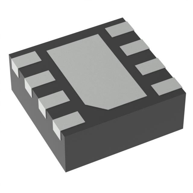
Small package footprint
– 8-Pin WSON (2 mm × 2 mm)
Each cell in a 2-series to 4-series cell stack is
individually monitored for an overvoltage condition. An
internally fixed-delay timer is initiated upon detection
of an overvoltage condition on any cell. Upon
expiration of the delay timer, an output pin is triggered
into an active state to indicate that an overvoltage
condition has occurred.
The regulated output supply delivers up to 2-mA
(max) output current to drive always-on circuits, such
as a real-time clock (RTC) oscillator. The BQ296xxx
family has a self-disable function to turn off the
regulated output if any cell voltage falls below a
certain threshold, thereby preventing drain on the
battery, and provides an external control to enable or
disable the regulated output.
Device Information
2 Applications
•
•
•
•
PART NUMBER
(1)
BQ2961
Notebook PC
Ultrabooks
Medical
UPS battery backup
BQ2962
(1)
PACKAGE
BODY SIZE (NOM)
WSON (8)
2.00 mm × 2.00 mm
For all available packages, see the orderable addendum at
the end of the data sheet.
Protector
FETs
Pack +
100 Ÿ
1 NŸ
VCELL4
1 NŸ 0.1 µF
VCELL3
1 NŸ 0.1 µF
VCELL2
VCELL1
1 NŸ
0.1 µF
0.1 µF
VDD
OUT
V4
REG
V3
VSS
5
(*)
* can be removed if Vss will be
connected first during cell
connection
V1
V2
External
Circuit
e.g., RTC
PWPD
0.1 µF 0.47 µF
Pack ±
Simplified Schematic
An IMPORTANT NOTICE at the end of this data sheet addresses availability, warranty, changes, use in safety-critical applications,
intellectual property matters and other important disclaimers. UNLESS OTHERWISE NOTED, this document contains PRODUCTION
DATA.
�BQ2961, BQ2962
www.ti.com
SLUSBU5T – NOVEMBER 2013 – REVISED AUGUST 2022
Table of Contents
1 Features............................................................................1
2 Applications..................................................................... 1
3 Description.......................................................................1
4 Revision History.............................................................. 2
5 Device Comparison Table...............................................3
6 Pin Configuration and Functions...................................4
7 Specifications.................................................................. 5
7.1 Absolute Maximum Ratings........................................ 5
7.2 ESD Ratings............................................................... 5
7.3 Recommended Operating Conditions.........................5
7.4 Thermal Information....................................................5
7.5 Electrical Characteristics.............................................6
7.6 Typical Characteristics................................................ 8
8 Detailed Description........................................................9
8.1 Overview..................................................................... 9
8.2 Functional Block Diagram......................................... 10
8.3 Feature Description...................................................10
8.4 Device Functional Modes..........................................11
9 Application and Implementation.................................. 13
9.1 Application Information............................................. 13
9.2 Typical Application.................................................... 13
10 Power Supply Recommendations..............................15
11 Layout........................................................................... 16
11.1 Layout Guidelines................................................... 16
11.2 Layout Example...................................................... 16
12 Device and Documentation Support..........................16
12.1 Third-Party Products Disclaimer............................. 16
12.2 Receiving Notification of Documentation Updates..16
12.3 Support Resources................................................. 16
12.4 Trademarks............................................................. 16
12.5 Electrostatic Discharge Caution..............................17
12.6 Glossary..................................................................17
13 Mechanical, Packaging, and Orderable
Information.................................................................... 17
4 Revision History
NOTE: Page numbers for previous revisions may differ from page numbers in the current version.
Changes from Revision S (June 2022) to Revision T (August 2022)
Page
• Noted in the Device Comparison Table that the increased UV range is for future BQ2962 devices only...........3
• Clarified future BQ2962 options..........................................................................................................................9
Changes from Revision R (April 2022) to Revision S (June 2022)
Page
• Increased the UV range for future BQ2962 device in the Device Comparison Table ........................................ 3
Changes from Revision Q (January 2022) to Revision R (April 2022)
Page
• Changed the BQ296234 device to Production Data in the Device Comparison Table ...................................... 3
Changes from Revision P (August 2021) to Revision Q (January 2022)
Page
• Added the BQ296234 PRODUCT PREVIEW device to the Device Comparison Table .................................... 3
Changes from Revision O (July 2021) to Revision P (August 2021)
Page
• Changed the BQ296227 and BQ296233 devices to Production Data in the Device Comparison Table ........... 3
2
Submit Document Feedback
Copyright © 2022 Texas Instruments Incorporated
Product Folder Links: BQ2961 BQ2962
�BQ2961, BQ2962
www.ti.com
SLUSBU5T – NOVEMBER 2013 – REVISED AUGUST 2022
5 Device Comparison Table
Table 5-1. BQ2961 Device Options
(1)
BQ2961
OVP (V)
OVP DELAY (s)
UV (V)
LDO (V)
BQ296100
4.35
6.5
2.5
3.3
BQ296103
4.50
6.5
2.5
3.3
BQ296106
4.45
6.5
2.8
3.3
BQ296107
4.50
6.5
2.8
3.3
BQ296111
4.45
4.0
2.5
3.3
BQ296112
4.50
3.0
2.5
3.3
BQ296113
4.35
3.0
2.5
3.3
BQ296114
4.50
4.0
2.5
3.3
2.5
BQ296115
4.25
6.5
2.0
BQ296116(1)
4.50
6.5
2.5
1.8
BQ2961
3.85 V–4.60 V (50-mV step)
3.0, 4.0, 5.5, 6.5
2.0 V–2.8 V (50-mV step)
1.8, 2.5, 3.3
PRODUCT PREVIEW. Contact TI for more information.
Table 5-2. BQ2962 Device Options
(1)
BQ2962
OVP (V)
OVP DELAY (s)
UV (V)
LDO (V)
BQ296202
4.45
6.5
2.5
3.3
BQ296203
4.50
6.5
2.5
3.3
BQ296212
4.50
3.0
2.5
3.3
BQ296213
4.35
3.0
2.5
3.3
BQ296215
4.50
6.5
2.5
3.0
BQ296216
4.55
6.5
2.5
3.0
BQ296217
4.55
6.5
2.8
3.3
BQ296221
4.55
6.5
2.5
3.3
BQ296222
4.50
6.5
3.0
3.0
BQ296223
4.50
6.5
2.5
3.3
BQ296224
4.50
6.5
2.5
3.0
BQ296226
4.50
6.5
2.8
3.3
BQ296227
4.55
6.5
2.8
3.3
BQ296228
4.55
6.5
2.5
3.0
bq296229
4.60
6.5
2.5
3.0
BQ296230
4.35
6.5
3.0
3.0
BQ296231
4.60
6.5
2.5
3.3
BQ296232
4.55
6.5
3.0
3.0
BQ296233
4.45
6.5
2.5
3.3
BQ296234
4.60
6.5
3.0
3.0
BQ2962(1)
3.85 V–4.60 V (50-mV step)
3.0, 4.0, 5.5, 6.5
2.0 V–3.5 V (50-mV step)
3, 3.15, 3.3
PRODUCT PREVIEW. Contact TI for more information.
Submit Document Feedback
Copyright © 2022 Texas Instruments Incorporated
Product Folder Links: BQ2961 BQ2962
3
�BQ2961, BQ2962
www.ti.com
SLUSBU5T – NOVEMBER 2013 – REVISED AUGUST 2022
6 Pin Configuration and Functions
1
VDD
OUT
8
2
V4
REG
7
3
V3
VSS
6
4
V2
V1
5
Figure 6-1. 2-Series to 4-Series BQ2961 (Top View)
1
VDD
REG
8
2
V4
OUT
7
3
V3
VSS
6
4
V2
V1
5
Figure 6-2. 2-Series to 4-Series BQ2962 (Top View)
Table 6-1. Pin Functions
PIN
DESCRIPTION
BQ2961
BQ2962
OUT
8
7
OA
PWPD
9
9
P
REG
7
8
OA
Regulated supply output. Requires an external ceramic capacitor for stability
REG_EN
—
—
IA
Regulated supply output enable. A "high" to enable REG output and "low" to
disable REG output
V1
5
5
IA
Sense input for positive voltage of the lowest cell from the bottom of the stack
V2
4
4
IA
Sense input for positive voltage of the second cell from the bottom of the stack
V3
3
3
IA
Sense input for positive voltage of the third cell from the bottom of the stack
(1)
4
(1)
TYPE
NAME
Analog output drive for an overvoltage fault signal; CMOS output high or opendrain active low
TI recommends connecting the exposed pad to VSS on PCB.
V4
2
2
IA
Sense input for positive voltage of the fourth cell from the bottom of the stack
VDD
1
1
P
Power supply input
VSS
6
6
P
Electrically connected to integrated circuit ground and negative terminal of the
lowest cell in the stack
IA = Analog input, OA = Analog Output, P = Power connection
Submit Document Feedback
Copyright © 2022 Texas Instruments Incorporated
Product Folder Links: BQ2961 BQ2962
�BQ2961, BQ2962
www.ti.com
SLUSBU5T – NOVEMBER 2013 – REVISED AUGUST 2022
7 Specifications
7.1 Absolute Maximum Ratings
Over operating free-air temperature range (unless otherwise noted)(1)
Supply voltage
Input voltage
Output voltage
MIN
MAX
VDD – VSS
–0.3
30
V4 – V3, V3 – V2, V2 – V1, V1 – VSS
–0.3
30
REG – VSS
–0.3
3.6
REG_EN – VSS
–0.3
28
OUT – VSS
–0.3
30
Continuous total power dissipation, PTOT
UNIT
V
See Section 7.4.
Lead temperature (soldering, 10 s), TSOLDER
300
300
°C
Storage temperature, Tstg
–65
150
°C
(1)
Operation outside the Absolute Maximum Ratings may cause permanent device damage. Absolute Maximum Ratings do not imply
functional operation of the device at these or any other conditions beyond those listed under Recommended Operating Conditions. If
outside the Recommended Operating Conditions but within the Absolute Maximum Ratings, the device may not be fully functional, and
this may affect device reliability, functionality, performance, and shorten the device lifetime.
7.2 ESD Ratings
VALUE
V(ESD)
(1)
(2)
Electrostatic discharge
Human body model (HBM), per ANSI/ESDA/JEDEC
JS-001(1)
UNIT
2000
Charged device model (CDM), per JEDEC specification JESD22-C101(2)
V
500
JEDEC document JEP155 states that 500-V HBM allows safe manufacturing with a standard ESD control process.
JEDEC document JEP157 states that 250-V CDM allows safe manufacturing with a standard ESD control process.
7.3 Recommended Operating Conditions
Over operating free-air temperature range (unless otherwise noted).
MIN
Supply voltage,
VDD (1)
Supply voltage, VDD (1)
3
Supply voltage, VDD with REG output on
4
Input voltage
range
Vn – Vn-1, V1 – VSS
0
REG_EN
Operating ambient temperature range, TA
(1)
NOM
MAX
20
5
UNIT
V
V
0
15
V
–40
110
°C
See Section 9.2.
7.4 Thermal Information
BQ296xxx
THERMAL METRIC(1)
DSG (WSON)
UNIT
8 PINS
RθJA
Junction-to-ambient thermal resistance
RθJC(top)
Junction-to-case(top) thermal resistance
RθJB
Junction-to-board thermal resistance
ψJT
Junction-to-top characterization parameter
1.6
°C/W
ψJB
Junction-to-board characterization parameter
33
°C/W
RθJC(bot)
Junction-to-case(bottom) thermal resistance
10
°C/W
(1)
62
°C/W
72
°C/W
32.5
°C/W
For more information about traditional and new thermal metrics, see the Semiconductor and IC Package Thermal Metrics application
report.
Submit Document Feedback
Copyright © 2022 Texas Instruments Incorporated
Product Folder Links: BQ2961 BQ2962
5
�BQ2961, BQ2962
www.ti.com
SLUSBU5T – NOVEMBER 2013 – REVISED AUGUST 2022
7.5 Electrical Characteristics
Typical values stated where TA = 25°C and VDD = 14.4 V, MIN/MAX values stated where TA = –40°C to +110°C, and VDD =
3 V to 15 V (unless otherwise noted).
PARAMETER
TEST CONDITIONS
MIN
TYP
MAX
UNIT
Voltage Protection Thresholds
VOV
V(PROTECT) Overvoltage
Detection
VHYS
OV Detection Hysteresis
VOA
OV Detection Accuracy
VOADRIFT
OV Detection Accuracy
Across Temperature
Applicable Voltage: 3.85 V to
4.6 V in 50-mV steps
RIN = 1 kΩ
250
300
V
400
mV
TA = 25°C
–10
10
mV
TA = –40°C
–40
40
mV
TA = 0°C
–20
20
mV
TA = 60°C
–24
24
mV
TA = 110°C
–54
54
mV
TA = 110°C
–54
54
mV
6
µA
8
µA
2
µA
4
µA
0.1
µA
8
V
Supply and Leakage Current
(Vn – Vn-1) = 2 V to 4.15 V, n =
Supply Current with REG 1 to 4, VDD = top Vn voltage
on
(V1 – VSS) > VUVREG , IREG = 0
mA,
TA = 0°C to 60°C
IDD
IDD
(Vn – Vn-1) = 2 V to 4.15 V, n =
Supply Current with REG
1 to 4, VDD = top Vn voltage
off
(V1 – VSS) < VUVREG
TA = 0°C to 60°C
IIN
Input Current at Vx Pins
4
TA = –40°C to 110°C
1
TA = –40°C to 110°C
(Vn – Vn-1) = (V1 – VSS) = 3.8 V, VDD = top Vn voltage,
TA = 25°C
–0.1
Output Drive OUT, CMOS Active High
(Vn – Vn-1) or (V1 – VSS) > VOV, IOH = 100 µA, VDD =
top Vn voltage
Output Drive Voltage,
Active High
VOUT
6
If three of four cells are short circuited, only one cell
remains powered and > VOV, VDD = Vn (the remaining
cell voltage), IOH = 100 µA
7
VDD –
0.3
(Vn – Vn-1) and (V1 – VSS) < VOV, VDD = sum of the
cell stack voltage, IOL = 100 µA measured into OUT pin
250
V
400
mV
4.5
mA
14
mA
3
3.6
s
IOUTH
OUT Source Current
(during OV)
(Vn – Vn-1), (V3 – V2), or (V1 – VSS) > VOV, VDD = top
Vn voltage,
forced OUT = 0 V, measured out of OUT pin
IOUTL
OUT Sink Current (no
OV)
(Vn – Vn-1) and (V1 – VSS) < VOV, VDD = top Vn
voltage, forced OUT = VDD, measured into OUT pin.
Pull-up resistor RPU = 5 kΩ to VDD
0.5
Internal Fixed Delay, 3-s delay option
2.4
Internal Fixed Delay, 4-s delay option
3.2
4
4.8
s
Internal Fixed Delay, 5.5-s delay option
4.4
5.5
6.6
s
Internal Fixed Delay, 6.5-s delay option
5.2
6.5
7.8
s
Internal Fixed Delay Timer
6
tDELAY
OV Delay Time(1)
tDELAY_CTM
Fault Detection Delay
Time in Test Mode OV
Delay Time
Internal Fixed Delay
15
ms
tDELAY_RESET
OV delay timer count
reset time; tDELAY resets
when the cell voltage
falls below VOV for
tDELAY_RESET.(1)
Internal Fixed Delay
0.6
ms
Submit Document Feedback
Copyright © 2022 Texas Instruments Incorporated
Product Folder Links: BQ2961 BQ2962
�BQ2961, BQ2962
www.ti.com
SLUSBU5T – NOVEMBER 2013 – REVISED AUGUST 2022
7.5 Electrical Characteristics (continued)
Typical values stated where TA = 25°C and VDD = 14.4 V, MIN/MAX values stated where TA = –40°C to +110°C, and VDD =
3 V to 15 V (unless otherwise noted).
PARAMETER
TEST CONDITIONS
MIN
TYP
MAX
VREG = 3.3 V,
3.234
3.300
3.366
VREG = 3.15 V,
BQ2962
3.087
3.150
3.213
VREG = 3.0 V,
BQ2962
2.940
3.000
3.060
VREG = 2.5 V,
BQ2961
2.450
2.500
2.550
VREG = 1.8 V,
BQ2961
1.764
1.800
1.836
VREG = 3.3 V,
BQ2961, BQ2962
3.200
3.300
3.400
VREG = 3.15 V,
BQ2962
3.050
3.150
3.250
VREG = 3.0 V,
BQ2962
2.900
3.000
3.100
VREG = 2.5 V,
BQ2961
2.425
2.500
2.575
VREG = 1.8 V,
BQ2961
1.746
1.800
1.854
UNIT
Regulated Supply Output, REG
REG Supply at
500 µA load
VREG
REG Supply from 0 to 2
mA load
VREG
VDD ≥ 4 V, IREG = 500 µA,
CREG = 0.47 µF
VDD ≥ 4 V, IREG = 0 µA to 2
mA,
CREG = 0.47 µF
IREG
REG Current Output
VDD ≥ 4 V, CREG = 0.47 µF
IREG_ SC_Limit
REG Output Short Circuit
REG = VSS, CREG = 0.47 µF
Current Limit
RREG_ PD
REG pull-down resistor
REG is disabled.
0
2
4
20
V
V
mA
mA
30
45
kΩ
Regulated Supply Output Enable, REG_EN
VIH
High-level Input
VIL
Low-level Input
ILKG
Input Leakage Current
1.6
V
VIH < 6 V
0.4
V
0.1
µA
50
mV
Regulated Supply Undervoltage Self-Disable
Factory Configuration: 2.0 V to 3.5 V in 50 mV steps,
TA = 25°C
VUVREG
Undervoltage detection
VUVHYS
Undervoltage Detection
Hysteresis
250
300
400
mV
tUVDELAY
Undervoltage Detection
Delay
4.5
6
7.5
s
VUVQUAL
Cell voltage to qualify for
UV detection
(1)
–50
0.5
V
Specified by design. Not 100% tested in production.
Submit Document Feedback
Copyright © 2022 Texas Instruments Incorporated
Product Folder Links: BQ2961 BQ2962
7
�BQ2961, BQ2962
www.ti.com
SLUSBU5T – NOVEMBER 2013 – REVISED AUGUST 2022
15
350
10
340
Overvoltage Hysteresis (mV)
Overvoltage Accuracy (mV)
7.6 Typical Characteristics
5
0
-5
-10
-15
Mean
Min
Max
-20
-25
-60
-40
-20
0
20
40
60
Temperature (qC)
80
100
330
320
310
300
290
280
-60
120
-40
0
20
40
60
Temperature (qC)
80
100
120
D002
Figure 7-2. Hysteresis VHYS vs. Temperature
5
5
4.5
Supply Current (PA)
0
-5
-10
-15
Mean
Min
Max
-20
-60
-40
-20
0
20
40
60
Temperature (qC)
80
100
4
3.5
3
Mean
Min
Max
2.5
2
-60
120
-40
-20
D003
Figure 7-3. Undervoltage Accuracy
0
20
40
60
Temperature (qC)
80
100
120
D004
Figure 7-4. IDD with Regulator On
1.4
3.31
1.2
Regulator Output (V)
3.305
Supply Current (PA)
-20
D001
Figure 7-1. Overvoltage Threshold (VOV) vs.
Temperature
Undervoltage Accuracy (mV)
Mean
Min
Max
1
0.8
0.6
0.4
Mean
Min
Max
3.3
3.295
3.29
Mean
Min
Max
0.2
0
-60
-40
-20
0
20
40
60
Temperature (qC)
80
100
D005
Figure 7-5. IDD with Regulator Off
8
120
3.285
-60
-40
-20
0
20
40
60
Temperature (qC)
80
100
120
D006
Figure 7-6. Regulator Output Without Load
Submit Document Feedback
Copyright © 2022 Texas Instruments Incorporated
Product Folder Links: BQ2961 BQ2962
�BQ2961, BQ2962
www.ti.com
SLUSBU5T – NOVEMBER 2013 – REVISED AUGUST 2022
8
Mean
Min
Max
-3.4
7
6
-3.45
Output Voltage (V)
High-Level Output Current (mA)
-3.35
-3.5
-3.55
-3.6
5
4
3
2
-3.65
-3.7
-60
1
-40
-20
0
20
40
60
Temperature (qC)
80
100
120
0
0
5
10
15
20
Supply Voltage (V)
D008
Figure 7-7. IOUTH vs Temperature
25
30
D009
Figure 7-8. VOUT vs VDD
8 Detailed Description
8.1 Overview
The BQ2961 and BQ2962 devices are second-level overvoltage (OV) protectors with a regulated output. Each
cell is monitored independently by comparing the actual cell voltage to an overvoltage threshold VOV. The
overvoltage threshold is preprogrammed at the factory with a range between 3.85 V to 4.65 V.
The regulated output is enabled unless any of the cell voltages fall below the VUVREG threshold. This threshold is
preprogrammed at the factory with a range between 2 V to 2.8 (3.5 V for future BQ2962 options).
Table 8-1. Programmable Parameters
OVERVOLTAGE RANGE (V)
3.85 to 4.6 in 50-mV steps
OVERVOLTAGE DELAY (s)
3, 4, 5.5, 6.5
UNDERVOLTAGE RANGE (V)
2.0 to 2.8 (3.5 for future BQ2962
options) in 50-mV steps
REGULATOR (V)
1.8, 2.5, 3.3 (BQ2961)
3.0, 3.15, 3.3 (BQ2962)
Submit Document Feedback
Copyright © 2022 Texas Instruments Incorporated
Product Folder Links: BQ2961 BQ2962
9
�BQ2961, BQ2962
www.ti.com
SLUSBU5T – NOVEMBER 2013 – REVISED AUGUST 2022
8.2 Functional Block Diagram
PACK+
R VD
C VD
VDD
1
Vref
V4
R IN
C IN
R IN
V3
3
C IN
R IN
V2
4
C IN
Multiplexer S witch Net work
2
Comp
+
UVP_Vref
7
REG_EN
Enable
V OV
Delay Charging/
Discharge circuit
5
C IN
-
REG
Programmable
setting
V1
R IN
+
Amp
-
Active
Delay
Timer
OUT
8
REG_EN
VSS
6
9
PWPD
PACK±
8.3 Feature Description
8.3.1 Pin Details
8.3.1.1 Input Sense Voltage, Vx
These inputs sense each battery cell voltage. A series resistor and a capacitor across the cell for each input is
required for noise filtering and stable voltage monitoring.
8.3.1.2 Output Drive, OUT
This terminal serves as the fault signal output in active high.
8.3.1.3 Supply Input, VDD
This terminal is the unregulated input power source for the device. A series resistor is connected to limit the
current, and a capacitor is connected to ground for noise filtering.
8.3.1.4 Regulated Supply Output, REG
This terminal is connected to an external capacitor and provides a regulated supply to power a circuit such as a
real-time clock integrated circuit, or functions requiring a well-regulated supply. Maximum current load on this pin
cannot exceed IREG mA.
The REG output has protection for overcurrent, using a current limit protection circuit, and also detects and
protects for excessive power dissipation due to short circuit of the external load. This pin requires a ceramic 1-µF
capacitor connection to VSS for improved stability, noise immunity, and ESD performance of the supply output.
This capacitor must be placed close to the REG and VSS pins for connection.
10
Submit Document Feedback
Copyright © 2022 Texas Instruments Incorporated
Product Folder Links: BQ2961 BQ2962
�BQ2961, BQ2962
www.ti.com
SLUSBU5T – NOVEMBER 2013 – REVISED AUGUST 2022
8.3.2 Overvoltage Sensing for OUT
Cell Voltage (V)
(V4-V3, V3-V2, V2-V1, V1-VSS)
In the BQ296xxx device, each cell is monitored independently. Overvoltage is detected by comparing the actual
cell voltage to a protection voltage reference, VOV. If any cell voltage exceeds the programmed OV value, an
internal timer circuit is activated. This timer circuit causes a factory pre-programmed fixed delay before the OUT
terminal goes from inactive to active state.
VOV
VOV - VHYS
tDELAY
OUT (V)
Figure 8-1. Timing for Overvoltage Sensing for OUT
8.3.3 Regulated Output Voltage and REG_EN Pin
For BQ2961, there are three factory-preprogrammed options for the regulated output voltage, 3.3 V, 2.5 V, and
1.8 V. For BQ2962, the regulated output voltage options are 3.3 V, 3.15 V, and 3.0 V. Potentially, the BQ2962xy
device can provide other regulated voltage output between 3.3 V to 3.0 V. Contact Texas Instruments for details.
At power up, the regulated output is on by default. If any cell voltage is below VUVREG at device power up, the
regulated output will remain on until the tUV_DELAY time has passed, the regulated output turns off after the delay
time.
Cell Voltage (V)
(V3-V2, V2-V1, V1-VSS)
During discharge, if any cell voltage falls below the VUVREG threshold for tUV_DELAY time, the regulated output is
self-disabled. The regulated output turns on again when all the cell voltages are above VUVREG + VUVHYS.
VUVREG + VUVHYS
VUVREG
tUVDELAY
REG (V)
Figure 8-2. REG Output Timing
8.4 Device Functional Modes
8.4.1 NORMAL Mode
When all of the cell voltages are below the VOV threshold AND above VUVREG threshold, the device operates
in NORMAL mode. The device monitors the differential cell voltages connected across (V1–VSS), (V2–V1), (V3–
V2), and (V4–V3). The OUT pin is inactive in this mode. The regulated output is always enabled for BQ2961.
8.4.2 OVERVOLTAGE Mode
OVERVOLTAGE mode is detected if any of the cell voltages exceed the overvoltage threshold, VOV, for a
configured OV delay time. The OUT pin is activated after a delay time preprogrammed at the factory. The OUT
Submit Document Feedback
Copyright © 2022 Texas Instruments Incorporated
Product Folder Links: BQ2961 BQ2962
11
�BQ2961, BQ2962
www.ti.com
SLUSBU5T – NOVEMBER 2013 – REVISED AUGUST 2022
pin will pull high internally. Then an external FET is turned on, shorting the fuse to ground, which allows the
battery and/or charger power to blow the fuse. When all of the cell voltages fall below (VOV – VHYS), the device
returns to NORMAL mode. The regulated output (if enabled) remains on in this mode.
8.4.3 UNDERVOLTAGE Mode
The UNDERVOLTAGE mode is detected if any of the cell voltage across (V1–VSS), (V2–V1), (V3–V2), or (V4–
V3) is below the VUVREG threshold for tUV_DELAY time. In this mode, the regulated output is disabled. To return to
the NORMAL mode, all the cell voltages must be above (VUVREG + VUVHYS).
For a low cell configuration, Vn pin can be shorted to the (Vn
voltage below VUVQUAL threshold for undervoltage detection.
– 1)
pin. The device ignores any differential cell
8.4.4 CUSTOMER TEST MODE
The Customer Test Mode (CTM) helps to reduce test time for checking the overvoltage delay-timer parameter
once the circuit is implemented into the battery pack. To enter CTM, the VDD pin should be set at least 10 V
higher than V3 (see Figure 8-3). The delay timer is greater than 10 ms, but considerably shorter than the timer
delay in normal operation. To exit CTM, remove the VDD to VC3 voltage differential of 10 V, so that the decrease
in the value automatically causes an exit.
CAUTION
Avoid exceeding any Absolute Maximum Voltages on any pins when placing the device into CTM.
Also avoid exceeding Absolute Maximum Voltages for the individual cell voltages (V3–V2), (V2–V1)
and (V1–VSS). Stressing the pins beyond the rated limits can cause permanent damage to the
device.
Figure 8-3 shows the timing for the Customer Test Mode.
VDD ± V3 = 10V
VDD
V3
> 10ms
OUT (V)
Figure 8-3. Timing for Customer Test Mode
Figure 8-4 shows the measurement for current consumption of the product for both VDD and Vx.
ICC
IIN
3.6 V
IIN
3.6 V
3.6 V
IIN
1 VDD
OUT 8
2 V3
REG 7
3 V2
VSS 6
4 V1
REG_EN 5
VDC
0.47 µF
Figure 8-4. Configuration for Integrated Circuit Current Consumption Test
12
Submit Document Feedback
Copyright © 2022 Texas Instruments Incorporated
Product Folder Links: BQ2961 BQ2962
�BQ2961, BQ2962
www.ti.com
SLUSBU5T – NOVEMBER 2013 – REVISED AUGUST 2022
9 Application and Implementation
Note
Information in the following applications sections is not part of the TI component specification, and
TI does not warrant its accuracy or completeness. TI’s customers are responsible for determining
suitability of components for their purposes. Customers should validate and test their design
implementation to confirm system functionality.
9.1 Application Information
The BQ296xxx family of second-level protectors is used for overvoltage protection of the battery pack in the
application. A regulated output is available to drive a small circuit with maximum IREG loading. The device OUT
pin is active high, which drives a NMOS FET that connects the fuse to ground in the event of a fault condition.
This provides a shorted path to use the battery and/or charger power to blow the fuse and cut the power path.
9.2 Typical Application
Application Schematic shows the recommended reference design components.
Protector
FETs
Pack +
100 Ÿ
1 NŸ
VCELL4
1 NŸ 0.1 µF
VCELL3
1 NŸ 0.1 µF
VCELL2
1 NŸ
VCELL1
0.1 µF
VDD
OUT
V4
REG
V3
VSS
5
External
Circuit
e.g., RTC
(*)
* can be removed if Vss will be
connected first during cell
connection
V1
V2
PWPD
0.1 µF 0.47 µF
0.1 µF
Pack ±
Figure 9-1. Application Schematic
9.2.1 Design Requirements
Note
Changes to the ranges shown in Table 9-1 will impact the accuracy of the cell measurements.
Table 9-1. Parameters
PARAMETER
EXTERNAL COMPONENT
Voltage monitor filter resistance
MIN
NOM
MAX
UNIT
RIN
900
1000
4700
Ω
Voltage monitor filter capacitance
CIN
0.01
0.1
1.0
µF
Supply voltage filter resistance
RVD
0.1
—
1
KΩ
Supply voltage filter capacitance
CVD
—
0.1
1.0
µF
REG output capacitance
CREG
0.47
1
—
µF
Note
The device is calibrated using an RIN value = 1 kΩ. Using a value other than the recommended value
changes the accuracy of the cell voltage measurements and VOV trigger level.
Submit Document Feedback
Copyright © 2022 Texas Instruments Incorporated
Product Folder Links: BQ2961 BQ2962
13
�BQ2961, BQ2962
www.ti.com
SLUSBU5T – NOVEMBER 2013 – REVISED AUGUST 2022
9.2.2 Detailed Design Procedure
Note
The device VSS must be connected first during PCB test or cell attachment. Failure to do so can
damage the REG pin.
1. If the VSS pin cannot be connected first, it is required to add a resistor of a minimum of 5 Ω to a maximum of
10 Ω (a 5-Ω resistor is used in the reference schematic, Figure 9-2) in series with the REG capacitor. When
VSS is floating, the REG capacitor always charges up to the VDD voltage. When VSS is finally connected,
the REG capacitor will be discharged. Adding a small resistor in series reduces the current strength and
avoids any potential damage to the REG pin. The 5-Ω resistor can be placed in series with the REG connect
circuit (as shown in Figure 9-2) or in series of the REG capacitor (as shown in Figure 9-3). Placing the
resistor in series with the REG circuit results in a small drop of VREG (for example: max loading of IREG mA
with a 5-Ω resistor will drop 5 mV on VREG), but such a connection can protect again rush current discharge
from a REG capacitor or an external filter capacitor connected to the REG pin. Placing the resistor in series
with the REG capacitor is an alternative to avoiding an additional drop in VREG if the filter capacitor used by
the external circuit is much smaller than the REG capacitor.
2. After VSS is connected, the device allows a random cell connection to the Vx pin.
3. The cell should be connected to the lower Vn pin; the unused Vn pin should be shorted to the (Vn-1) pin. See
Figure 9-2 for details.
Protector
FETs
Pack +
100 Ÿ
1 NŸ
VCELL3
0.1 µF
1 NŸ
VCELL2
0.1 µF
VCELL1
1 NŸ
0.1 µF
VDD
OUT
V4
V3
REG
bq2961
bq2962
V2
External
Circuit
e.g., RTC
5 Ÿ (*)
VSS
V1
PWPD
0.1 µF
0.47 µF
Pack ±
Copyright © 2017, Texas Instruments Incorporated
Figure 9-2. 3-Series BQ2961 and BQ2962 Schematic
4. A Zener diode can be added to the REG pin to VSS, as shown in Figure 9-3. This is recommended to protect
the circuit connected to the REG pin if floating VSS in the field is a risk concern. When VSS is floating
(during cell connection when VSS is not connected first or in a system fault with a broken BAT– wire), the
REG voltage always pulls up to VDD. In a 4-series configuration, the REG voltage can reach approximately
16 V with VSS floating. Adding a Zener diode clamps the REG voltage to a safe level for the external circuits
connected to the REG pin. Having the Zener diode can also protect the external circuits if the REG pin is
shorted to the OUT pin or any other high-voltage output terminal. If a Zener diode is used, TI recommends
putting the diode on the battery side with the BQ296xxx device to allow protection on the REG pin, as well as
the circuit connected to REG under the floating VSS condition. The resistor in series with the REG pin is not
required in this case.
14
Submit Document Feedback
Copyright © 2022 Texas Instruments Incorporated
Product Folder Links: BQ2961 BQ2962
�BQ2961, BQ2962
www.ti.com
SLUSBU5T – NOVEMBER 2013 – REVISED AUGUST 2022
REG
The 5-Ÿ UHVLVWRU OLPLWV WKH UXVK FXUUHQW
discharge from the capacitor during cell
connection when Vss is not connected
first.
Loss of Vss connection or REG shorted to
high voltage can bring the REG above the
regulated range. This optional zener
clamp can protect the downstream circuit
under such an event.
5Ÿ
0.47 µF
This resistor is not required if Vss is
connected first in the cell connection
sequence.
Figure 9-3. 5-V Zener Diode
9.2.3 Application Curves
Figure 9-4. Overvoltage Protection
Figure 9-5. Overvoltage Protection Release
Figure 9-6. Undervoltage Detection to Turn Off the
Regulator
Figure 9-7. Undervoltage Release to Switch On the
Regulator
10 Power Supply Recommendations
The maximum power is 20 V for BQ2961 and BQ2962 on VDD.
Note
Connect VSS first during power-up.
Submit Document Feedback
Copyright © 2022 Texas Instruments Incorporated
Product Folder Links: BQ2961 BQ2962
15
�BQ2961, BQ2962
www.ti.com
SLUSBU5T – NOVEMBER 2013 – REVISED AUGUST 2022
11 Layout
11.1 Layout Guidelines
Use the following layout guidelines:
1. Ensure the RC filters for the Vx pins and VDD pin are placed as close as possible to the target terminal,
reducing the tracing loop area.
2. The capacitor for REG should be placed close to the device terminals.
3. Ensure the trace connecting the fuse to the gate, source of the NFET to the Pack– is sufficient to withstand
the current during a fuse blown event.
11.2 Layout Example
Place the RC filters close
to device terminals
Power Trace Line
VDD
OUT
V4
REG
V3
VCELL3
V2
VCELL2
PWPD
VSS
Pack +
5
(*)
External
Circuit
e.g., RTC
Pack ±
V1
VCELL1
* can be removed if Vss
will be connected first
during cell connection
Ensure trace can support sufficient
current flow for fuse blow
Figure 11-1. Layout Example
12 Device and Documentation Support
12.1 Third-Party Products Disclaimer
TI'S PUBLICATION OF INFORMATION REGARDING THIRD-PARTY PRODUCTS OR SERVICES DOES NOT
CONSTITUTE AN ENDORSEMENT REGARDING THE SUITABILITY OF SUCH PRODUCTS OR SERVICES
OR A WARRANTY, REPRESENTATION OR ENDORSEMENT OF SUCH PRODUCTS OR SERVICES, EITHER
ALONE OR IN COMBINATION WITH ANY TI PRODUCT OR SERVICE.
12.2 Receiving Notification of Documentation Updates
To receive notification of documentation updates, navigate to the device product folder on ti.com. In the upper
right corner, click on Alert me to register and receive a weekly digest of any product information that has
changed. For change details, review the revision history included in any revised document.
12.3 Support Resources
TI E2E™ support forums are an engineer's go-to source for fast, verified answers and design help — straight
from the experts. Search existing answers or ask your own question to get the quick design help you need.
Linked content is provided "AS IS" by the respective contributors. They do not constitute TI specifications and do
not necessarily reflect TI's views; see TI's Terms of Use.
12.4 Trademarks
TI E2E™ is a trademark of Texas Instruments.
All trademarks are the property of their respective owners.
16
Submit Document Feedback
Copyright © 2022 Texas Instruments Incorporated
Product Folder Links: BQ2961 BQ2962
�BQ2961, BQ2962
www.ti.com
SLUSBU5T – NOVEMBER 2013 – REVISED AUGUST 2022
12.5 Electrostatic Discharge Caution
This integrated circuit can be damaged by ESD. Texas Instruments recommends that all integrated circuits be handled
with appropriate precautions. Failure to observe proper handling and installation procedures can cause damage.
ESD damage can range from subtle performance degradation to complete device failure. Precision integrated circuits may
be more susceptible to damage because very small parametric changes could cause the device not to meet its published
specifications.
12.6 Glossary
TI Glossary
This glossary lists and explains terms, acronyms, and definitions.
13 Mechanical, Packaging, and Orderable Information
The following pages include mechanical, packaging, and orderable information. This information is the most
current data available for the designated devices. This data is subject to change without notice and revision of
this document. For browser-based versions of this data sheet, refer to the left-hand navigation.
Submit Document Feedback
Copyright © 2022 Texas Instruments Incorporated
Product Folder Links: BQ2961 BQ2962
17
�PACKAGE OPTION ADDENDUM
www.ti.com
19-Nov-2022
PACKAGING INFORMATION
Orderable Device
Status
(1)
Package Type Package Pins Package
Drawing
Qty
Eco Plan
(2)
Lead finish/
Ball material
MSL Peak Temp
Op Temp (°C)
Device Marking
(3)
Samples
(4/5)
(6)
BQ296100DSGR
ACTIVE
WSON
DSG
8
3000
RoHS & Green
NIPDAU
Level-2-260C-1 YEAR
-40 to 110
6100
Samples
BQ296100DSGT
ACTIVE
WSON
DSG
8
250
RoHS & Green
NIPDAU
Level-2-260C-1 YEAR
-40 to 110
6100
Samples
BQ296103DSGR
ACTIVE
WSON
DSG
8
3000
RoHS & Green
NIPDAU
Level-1-260C-UNLIM
-40 to 110
6103
Samples
BQ296103DSGT
ACTIVE
WSON
DSG
8
250
RoHS & Green
NIPDAU
Level-1-260C-UNLIM
-40 to 110
6103
Samples
BQ296106DSGR
ACTIVE
WSON
DSG
8
3000
RoHS & Green
NIPDAU
Level-1-260C-UNLIM
-40 to 110
6106
Samples
BQ296106DSGT
ACTIVE
WSON
DSG
8
250
RoHS & Green
NIPDAU
Level-1-260C-UNLIM
-40 to 110
6106
Samples
BQ296107DSGR
ACTIVE
WSON
DSG
8
3000
RoHS & Green
NIPDAU
Level-1-260C-UNLIM
-40 to 110
6107
Samples
BQ296107DSGT
ACTIVE
WSON
DSG
8
250
RoHS & Green
NIPDAU
Level-1-260C-UNLIM
-40 to 110
6107
Samples
BQ296111DSGR
ACTIVE
WSON
DSG
8
3000
RoHS & Green
NIPDAU
Level-2-260C-1 YEAR
-40 to 110
6111
Samples
BQ296111DSGT
ACTIVE
WSON
DSG
8
250
RoHS & Green
NIPDAU
Level-2-260C-1 YEAR
-40 to 110
6111
Samples
BQ296112DSGR
ACTIVE
WSON
DSG
8
3000
RoHS & Green
NIPDAU
Level-2-260C-1 YEAR
-40 to 110
6112
Samples
BQ296112DSGT
ACTIVE
WSON
DSG
8
250
RoHS & Green
NIPDAU
Level-2-260C-1 YEAR
-40 to 110
6112
Samples
BQ296113DSGR
ACTIVE
WSON
DSG
8
3000
RoHS & Green
NIPDAU
Level-1-260C-UNLIM
-40 to 110
6113
Samples
BQ296113DSGT
ACTIVE
WSON
DSG
8
250
RoHS & Green
NIPDAU
Level-1-260C-UNLIM
-40 to 110
6113
Samples
BQ296114DSGR
ACTIVE
WSON
DSG
8
3000
RoHS & Green
NIPDAU
Level-2-260C-1 YEAR
-40 to 110
6114
Samples
BQ296114DSGT
ACTIVE
WSON
DSG
8
250
RoHS & Green
NIPDAU
Level-2-260C-1 YEAR
-40 to 110
6114
Samples
BQ296115DSGR
ACTIVE
WSON
DSG
8
3000
RoHS & Green
NIPDAU
Level-2-260C-1 YEAR
-40 to 110
6115
Samples
BQ296202DSGR
ACTIVE
WSON
DSG
8
3000
RoHS & Green
NIPDAU
Level-1-260C-UNLIM
-40 to 110
6202
Samples
BQ296202DSGT
ACTIVE
WSON
DSG
8
250
RoHS & Green
NIPDAU
Level-1-260C-UNLIM
-40 to 110
6202
Samples
BQ296203DSGR
ACTIVE
WSON
DSG
8
3000
RoHS & Green
NIPDAU
Level-1-260C-UNLIM
-40 to 110
6203
Samples
Addendum-Page 1
�PACKAGE OPTION ADDENDUM
www.ti.com
Orderable Device
19-Nov-2022
Status
(1)
Package Type Package Pins Package
Drawing
Qty
Eco Plan
(2)
Lead finish/
Ball material
MSL Peak Temp
Op Temp (°C)
Device Marking
(3)
Samples
(4/5)
(6)
BQ296203DSGT
ACTIVE
WSON
DSG
8
250
RoHS & Green
NIPDAU
Level-1-260C-UNLIM
-40 to 110
6203
Samples
BQ296212DSGR
ACTIVE
WSON
DSG
8
3000
RoHS & Green
NIPDAU
Level-2-260C-1 YEAR
-40 to 110
6212
Samples
BQ296212DSGT
ACTIVE
WSON
DSG
8
250
RoHS & Green
NIPDAU
Level-2-260C-1 YEAR
-40 to 110
6212
Samples
BQ296213DSGR
ACTIVE
WSON
DSG
8
3000
RoHS & Green
NIPDAU
Level-2-260C-1 YEAR
-40 to 110
6213
Samples
BQ296213DSGT
ACTIVE
WSON
DSG
8
250
RoHS & Green
NIPDAU
Level-2-260C-1 YEAR
-40 to 110
6213
Samples
BQ296215DSGR
ACTIVE
WSON
DSG
8
3000
RoHS & Green
NIPDAU
Level-1-260C-UNLIM
-40 to 110
6215
Samples
BQ296215DSGT
ACTIVE
WSON
DSG
8
250
RoHS & Green
NIPDAU
Level-1-260C-UNLIM
-40 to 110
6215
Samples
BQ296216DSGR
ACTIVE
WSON
DSG
8
3000
RoHS & Green
NIPDAU
Level-1-260C-UNLIM
-40 to 110
6216
Samples
BQ296216DSGT
ACTIVE
WSON
DSG
8
250
RoHS & Green
NIPDAU
Level-1-260C-UNLIM
-40 to 110
6216
Samples
BQ296217DSGR
ACTIVE
WSON
DSG
8
3000
RoHS & Green
NIPDAU
Level-1-260C-UNLIM
-40 to 110
6217
Samples
BQ296217DSGT
ACTIVE
WSON
DSG
8
250
RoHS & Green
NIPDAU
Level-1-260C-UNLIM
-40 to 110
6217
Samples
BQ296221DSGR
ACTIVE
WSON
DSG
8
3000
RoHS & Green
NIPDAU
Level-2-260C-1 YEAR
-40 to 110
6221
Samples
BQ296221DSGT
ACTIVE
WSON
DSG
8
250
RoHS & Green
NIPDAU
Level-2-260C-1 YEAR
-40 to 110
6221
Samples
BQ296222DSGR
ACTIVE
WSON
DSG
8
3000
RoHS & Green
NIPDAU
Level-1-260C-UNLIM
-40 to 110
6222
Samples
BQ296222DSGT
ACTIVE
WSON
DSG
8
250
RoHS & Green
NIPDAU
Level-1-260C-UNLIM
-40 to 110
6222
Samples
BQ296223DSGR
ACTIVE
WSON
DSG
8
3000
RoHS & Green
NIPDAU
Level-1-260C-UNLIM
-40 to 110
6223
Samples
BQ296223DSGT
ACTIVE
WSON
DSG
8
250
RoHS & Green
NIPDAU
Level-1-260C-UNLIM
-40 to 110
6223
Samples
BQ296224DSGR
ACTIVE
WSON
DSG
8
3000
RoHS & Green
NIPDAU
Level-1-260C-UNLIM
-40 to 110
6224
Samples
BQ296224DSGT
ACTIVE
WSON
DSG
8
250
RoHS & Green
NIPDAU
Level-1-260C-UNLIM
-40 to 110
6224
Samples
BQ296226DSGR
ACTIVE
WSON
DSG
8
3000
RoHS & Green
NIPDAU
Level-1-260C-UNLIM
-40 to 110
6226
Samples
BQ296226DSGT
ACTIVE
WSON
DSG
8
250
RoHS & Green
NIPDAU
Level-1-260C-UNLIM
-40 to 110
6226
Samples
Addendum-Page 2
�PACKAGE OPTION ADDENDUM
www.ti.com
Orderable Device
19-Nov-2022
Status
(1)
Package Type Package Pins Package
Drawing
Qty
Eco Plan
(2)
Lead finish/
Ball material
MSL Peak Temp
Op Temp (°C)
Device Marking
(3)
Samples
(4/5)
(6)
BQ296227DSGR
ACTIVE
WSON
DSG
8
3000
RoHS & Green
NIPDAU
Level-2-260C-1 YEAR
-40 to 110
6227
Samples
BQ296228DSGR
ACTIVE
WSON
DSG
8
3000
RoHS & Green
NIPDAU
Level-1-260C-UNLIM
-40 to 110
6228
Samples
BQ296228DSGT
ACTIVE
WSON
DSG
8
250
RoHS & Green
NIPDAU
Level-1-260C-UNLIM
-40 to 110
6228
Samples
BQ296229DSGR
ACTIVE
WSON
DSG
8
3000
RoHS & Green
NIPDAU
Level-1-260C-UNLIM
-40 to 110
6229
Samples
BQ296229DSGT
ACTIVE
WSON
DSG
8
250
RoHS & Green
NIPDAU
Level-1-260C-UNLIM
-40 to 110
6229
Samples
BQ296230DSGR
ACTIVE
WSON
DSG
8
3000
RoHS & Green
NIPDAU
Level-1-260C-UNLIM
-40 to 110
6230
Samples
BQ296230DSGT
ACTIVE
WSON
DSG
8
250
RoHS & Green
NIPDAU
Level-1-260C-UNLIM
-40 to 110
6230
Samples
BQ296231DSGR
ACTIVE
WSON
DSG
8
3000
RoHS & Green
NIPDAU
Level-1-260C-UNLIM
-40 to 110
6231
Samples
BQ296231DSGT
ACTIVE
WSON
DSG
8
250
RoHS & Green
NIPDAU
Level-1-260C-UNLIM
-40 to 110
6231
Samples
BQ296232DSGR
ACTIVE
WSON
DSG
8
3000
RoHS & Green
NIPDAU
Level-1-260C-UNLIM
-40 to 110
6232
Samples
BQ296232DSGT
ACTIVE
WSON
DSG
8
250
RoHS & Green
NIPDAU
Level-1-260C-UNLIM
-40 to 110
6232
Samples
BQ296233DSGR
ACTIVE
WSON
DSG
8
3000
RoHS & Green
NIPDAU
Level-2-260C-1 YEAR
-40 to 110
6233
Samples
BQ296234DSGR
ACTIVE
WSON
DSG
8
3000
RoHS & Green
NIPDAU
Level-1-260C-UNLIM
-40 to 110
6234
Samples
(1)
The marketing status values are defined as follows:
ACTIVE: Product device recommended for new designs.
LIFEBUY: TI has announced that the device will be discontinued, and a lifetime-buy period is in effect.
NRND: Not recommended for new designs. Device is in production to support existing customers, but TI does not recommend using this part in a new design.
PREVIEW: Device has been announced but is not in production. Samples may or may not be available.
OBSOLETE: TI has discontinued the production of the device.
(2)
RoHS: TI defines "RoHS" to mean semiconductor products that are compliant with the current EU RoHS requirements for all 10 RoHS substances, including the requirement that RoHS substance
do not exceed 0.1% by weight in homogeneous materials. Where designed to be soldered at high temperatures, "RoHS" products are suitable for use in specified lead-free processes. TI may
reference these types of products as "Pb-Free".
RoHS Exempt: TI defines "RoHS Exempt" to mean products that contain lead but are compliant with EU RoHS pursuant to a specific EU RoHS exemption.
Green: TI defines "Green" to mean the content of Chlorine (Cl) and Bromine (Br) based flame retardants meet JS709B low halogen requirements of


 工商网监
湘ICP备2023018690号
工商网监
湘ICP备2023018690号

