BQ2980, BQ2982
SLUSCS3I – OCTOBER 2017 – REVISED NOVEMBER 2021
BQ298xyz Voltage, Current, Temperature Protectors with an Integrated High-Side
NFET Driver for Fast/Flash Charging Single-Cell Li-Ion and Li-Polymer Batteries
1 Features
3 Description
•
The BQ298xyz family of devices, featuring integrated
charge-pump FET drivers, provides high-side primary
battery cell protection for 1-series Li-ion and LiPolymer batteries, enabling consistent Rdson across
cell voltages. For better system thermal performance,
the BQ298x device's accuracy enables the use of a
sense resistor as low as 1 mΩ.
•
•
•
•
•
Voltage protection:
– Overvoltage (OV): ±10 mV
– Undervoltage (UV): ±20 mV
Current protection:
– Overcurrent in charge (OCC): ±1 mV
– Overcurrent in discharge (OCD): ±1 mV
– Short circuit in discharge (SCD): ±5 mV
Temperature protection:
– Overtemperature (OT)
Additional features:
– Supports as low as a 1-mΩ sense resistor
(RSNS)
– High-side protection
– High Vgs FET drive
– 0-V charging (only BQ2980)
– CTR pin for FET override control for system
reset/shutdown
– Configure CTR for second OT protection
through an external PTC thermistor
Current consumption:
– NORMAL mode: 4 µA
– SHUTDOWN mode: 0.1-µA maximum
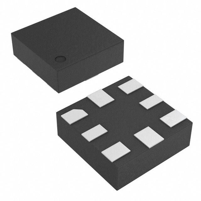
Package:
– 8-pin X2QFN: 1.50 × 1.50 × 0.37 mm
The CTR pin in the BQ298x device can be configured
to override the FET driver by host control to create a
system reset or shutdown function. Alternatively, the
CTR pin can be configured to connect an external
Positive Temperature Coefficient (PTC) thermistor for
FET OT protection in addition to the internal die
temperature sensor. The BQ2980xy devices support
zero-volt (0-V) charging, while the BQ2982xy devices
have this disabled.
Device Information
PART
NUMBER(1)
PACKAGE
BODY SIZE (NOM)
BQ2980xy
X2QFN
1.50 mm × 1.50 mm × 0.37 mm
BQ2982xy
X2QFN
1.50 mm × 1.50 mm × 0.37 mm
(1)
For all available packages, see the orderable addendum and
Device Comparison Table.
2 Applications
Smartphones
Tablets
Power bank
Wearables
Option to configure for PTC protection
RBAT
BAT
CHG
VDD
DSG
VSS
PACK
CS
CVDD
CTR
RPACK
CTR
PTC
•
•
•
•
PACK+
RVDD
VSS
PACK–
RCTR
System
Reset
Scale RC values for
system reset timing
PACK–
RSNS
Simplified Schematic
An IMPORTANT NOTICE at the end of this data sheet addresses availability, warranty, changes, use in safety-critical applications,
intellectual property matters and other important disclaimers. PRODUCTION DATA.
�BQ2980, BQ2982
www.ti.com
SLUSCS3I – OCTOBER 2017 – REVISED NOVEMBER 2021
Table of Contents
1 Features............................................................................1
2 Applications..................................................................... 1
3 Description.......................................................................1
4 Revision History.............................................................. 2
5 Device Comparison Table...............................................3
6 Pin Configuration and Functions...................................3
7 Specifications.................................................................. 4
7.1 Absolute Maximum Ratings........................................ 4
7.2 ESD Ratings............................................................... 4
7.3 Recommended Operating Conditions.........................4
7.4 Thermal Information....................................................4
7.5 Electrical Characteristics.............................................5
7.6 Typical Characteristics................................................ 8
8 Detailed Description........................................................9
8.1 Overview..................................................................... 9
8.2 Functional Block Diagram......................................... 10
8.3 Feature Description...................................................10
8.4 Device Functional Modes..........................................13
9 Application and Implementation.................................. 14
9.1 Application Information............................................. 14
9.2 Typical Applications.................................................. 17
10 Power Supply Recommendations..............................20
11 Layout........................................................................... 20
11.1 Layout Guidelines................................................... 20
11.2 Layout Example...................................................... 20
12 Device and Documentation Support..........................21
12.1 Third-Party Products Disclaimer............................. 21
12.2 Receiving Notification of Documentation Updates..21
12.3 Support Resources................................................. 21
12.4 Trademarks............................................................. 21
12.5 Electrostatic Discharge Caution..............................21
12.6 Glossary..................................................................21
13 Mechanical, Packaging, and Orderable
Information.................................................................... 21
4 Revision History
NOTE: Page numbers for previous revisions may differ from page numbers in the current version.
Changes from Revision H (July 2021) to Revision I (November 2021)
Page
• Changed the Device Comparison Table ............................................................................................................ 3
Changes from Revision G (May 2021) to Revision H (July 2021)
Page
• Changed the BQ298019 device from PRODUCT PREVIEW to Production Data in the Device Comparison
Table .................................................................................................................................................................. 3
Changes from Revision F (December 2020) to Revision G (May 2021)
Page
• Removed "Product Preview" footnote from BQ2982 in Description .................................................................. 1
• Changed the Device Comparison Table ............................................................................................................ 3
• Removed PRODUCT PREVIEW footnote from BQ2982xy in Thermal Information .......................................... 4
• Clarified CHG driver at low VDD in Electrical Characteristics ........................................................................... 5
• Clarified VDD condition in Charge and Discharge Driver .................................................................................11
• Clarified ZVCHG in ZVCHG (0-V Charging) .................................................................................................... 13
2
Submit Document Feedback
Copyright © 2021 Texas Instruments Incorporated
Product Folder Links: BQ2980 BQ2982
�BQ2980, BQ2982
www.ti.com
SLUSCS3I – OCTOBER 2017 – REVISED NOVEMBER 2021
5 Device Comparison Table
BQ298xyz Device Family (BQ2980xy with ZVCHG [0-V Charging] Enabled, BQ2982xy with ZVCHG Disabled)
PART
NUMBER
OVP (V)
OVP
DELAY
(s)
UVP
(V)
UVP
DELAY
(ms)
OCD
DELAY
(ms)
SCD
(mV)
SCD
DELAY (µs)
OT (°C)
CTR/
PTC Config
UV_Shut
BQ298000
4.475
1.25
2.600
144
–8
8
BQ298006
4.475
1.00
2.500
20
–12
16
8
8
20
250 Fixed
85
CTR
Enabled
14
16
40
250 Fixed
75
CTR
Enabled
BQ298009
4.500
1.00
2.900
20
–18
8
BQ298010
4.500
1.00
2.900
20
–10
8
30
16
40
250 Fixed
Disable
CTR
Enabled
20
16
30
250 Fixed
Disable
CTR
BQ298012
4.300
1.00
2.750
144
–4
Enabled
8
14
20
30
250 Fixed
Disable
CTR
BQ298015
4.440
1.25
2.800
144
Enabled
–8
8
8
8
20
250 Fixed
85
CTR
BQ298018
4.400
1.00
2.700
Enabled
144
–8
8
20
48
60
250 Fixed
85
CTR
BQ298019
4.425
1.25
Enabled
2.800
144
–30
48
8
48
40
250 Fixed
85
CTR
Enabled
BQ298215
4.440
BQ298216
4.300
1.25
2.800
144
–8
8
8
8
20
250 Fixed
85
CTR
Enabled
1.00
2.500
144
–4
8
14
20
30
250 Fixed
Disabled
CTR
Enabled
OCC
(mV)
OCC
DELAY
(ms)
OCD
(mV)
CHG
6 Pin Configuration and Functions
1
VDD
2
VSS
3
7
DSG
6
PACK
5
CTR
CS
4
8
BAT
Not to scale
Figure 6-1. RUG Package 8-Pin X2QFN Top View
Table 6-1. Pin Functions
NUMBER
(1)
NAME
TYPE
1
BAT
I(1)
DESCRIPTION
BAT voltage sensing input (connected to the battery side)
2
VDD
P
Supply voltage
3
VSS
—
Device ground
4
CS
I
Current sensing input (connect to PACK– side of the sense resistor)
5
CTR
I
Active high control pin to open FET drivers and shut down the device. It can be configured to
enable an internal pull-up and connect the CTR pin to an external PTC for OT protection.
6
PACK
I
Pack voltage sensing pin (connected to the charger side, typically referred to as PACK+ and
PACK–)
7
DSG
O
DSG FET driver
8
CHG
O
CHG FET driver
I = input, O = output, P = power
Submit Document Feedback
Copyright © 2021 Texas Instruments Incorporated
Product Folder Links: BQ2980 BQ2982
3
�BQ2980, BQ2982
www.ti.com
SLUSCS3I – OCTOBER 2017 – REVISED NOVEMBER 2021
7 Specifications
7.1 Absolute Maximum Ratings
over operating free-air temperature range (unless otherwise noted)(1)
Supply voltage
Input voltage
Output voltage
MIN
MAX
UNIT
VDD
–0.3
6
V
PACK
–0.3
24
BAT
–0.3
6
CS
–0.3
0.3
CTR
–0.3
5
CHG
–0.3
20
DSG
–0.3
20
–55
150
Storage temperature, Tstg
(1)
V
V
°C
Operation outside the Absolute Maximum Ratings may cause permanent device damage. Absolute Maximum Ratings do not imply
functional operation of the device at these or any other conditions beyond those listed under Recommended Operating Conditions. If
outside the Recommended Operating Conditions but within the Absolute Maximum Ratings, the device may not be fully functional, and
this may affect device reliability, functionality, performance, and shorten the device lifetime.
7.2 ESD Ratings
VALUE
V(ESD)
(1)
(2)
JS-001(1)
Human-body model (HBM), per ANSI/ESDA/JEDEC
Electrostatic discharge
±1000
Charged-device model (CDM), per JEDEC specification JESD22-C101(2)
±250
UNIT
V
JEDEC document JEP155 states that 500-V HBM allows safe manufacturing with a standard ESD control process.
JEDEC document JEP157 states that 250-V CDM allows safe manufacturing with a standard ESD control process.
7.3 Recommended Operating Conditions
over operating free-air temperature range (unless otherwise noted)
Supply voltage
VDD
PACK
Input voltage
Output voltage
MIN
MAX
UNIT
1.5
5.5
V
0
20
BAT
1.5
5.5
CS
–0.25
0.25
CTR
0
5
CHG
VSS
VDD + VDD × AFETON
DSG
VSS
VDD + VDD × AFETON
–40
85
Operating temperature, TA
V
V
°C
7.4 Thermal Information
BQ2980xy/BQ2982xy
THERMAL METRIC(1)
RUG (X2QFN)
UNIT
8 PINS
RθJA
Junction-to-ambient thermal resistance
RθJC(top)
Junction-to-case (top) thermal resistance
RθJB
Junction-to-board thermal resistance
ψJT
ψJB
(1)
4
171.8
°C/W
75
°C/W
94.7
°C/W
Junction-to-top characterization parameter
2.5
°C/W
Junction-to-board characterization parameter
94.9
°C/W
For more information about traditional and new thermal metrics, see the Semiconductor and IC Package Thermal Metrics application
report.
Submit Document Feedback
Copyright © 2021 Texas Instruments Incorporated
Product Folder Links: BQ2980 BQ2982
�BQ2980, BQ2982
www.ti.com
SLUSCS3I – OCTOBER 2017 – REVISED NOVEMBER 2021
7.5 Electrical Characteristics
Typical values stated at TA = 25°C and VDD = 3.6 V. MIN/MAX values stated with TA = –40°C to +85°C and VDD = 3 to 5 V
unless otherwise noted.
PARAMETER
TEST CONDITIONS
MIN
TYP
MAX
UNIT
VCHG and VDSG > 5 V, CLOAD = 8 nF (typical 20 nA(1)),
VDD > 4.0 V
5
8
µA
VCHG and VDSG > 5 V, CLOAD = 8 nF (typical 20 nA(1)),
UVP < VDD < 3.9 V
4
6
µA
2
4
µA
0.1
µA
SUPPLY CURRENT CONSUMPTION
INORMAL
Normal mode supply current
IFETOFF
Supply current with both
FET drivers off
VCHG = VDSG ≤ 0.2 V
ISHUT
Shutdown current
VPACK < VBAT, VDD = 1.5 V
N-CH FET DRIVER, CHG and DSG
AFETON
FET driver gain factor, the
Vgs voltage to FET
VCHG or VDSG = VDD + VDD × AFETON
UVP < VDD < 3.9 V
CLOAD = 8 nF
1.65
1.75
1.81
V/V
VCHG or VDSG = VDD + VDD × AFETON
VDD > 4.0 V
CLOAD = 8 nF
1.45
1.55
1.68
V/V
0.2
V
2.1
V
VFETOFF
FET driver off output voltage
VFETOFF = VCHG – VSS or VDSG – VSS
CLOAD = 8 nF
VDRIVER_SHUT
FET driver charge pump
shut down voltage
Charge pump enabled when VDD rises to
VDRIVER_SHUT
FET driver charge pump
shut down voltage
hysteresis
Charge pump disabled when VDD falls to
VDRIVER_SHUT – VDRIVER_SHUT_HYS
trise (2)
FET driver rise time
CLOAD = 8 nF,
VCHG or VDSG rises from VDD to (2 × VDD)
tfall
FET driver fall time
CLOAD = 8 nF,
VCHG or VDSG fall to VFETOFF
ILOAD
FET driver maximum loading
VDRIVER_SHUT
_HYS
1.95
2
50
mV
400
800
µs
50
200
µs
10
µA
mV
VOLTAGE PROTECTION
VOVP
VOVP_ACC
Overvoltage detection range Factory configured, 50-mV step
Overvoltage detection
accuracy
3750
5200
TA = 25°C, CHG/DSG CLOAD < 1 µA
–10
10
TA = 0°C to 60°C, CHG/DSG CLOAD < 1 µA
–15
15
TA = –40°C to +85°C, CHG/DSG CLOAD < 1 µA
–25
25
150
VOVP_HYS
Overvoltage release
hysteresis voltage
Fixed at 200 mV
VUVP
Undervoltage detection
range
Factory configured, 50-mV step
VUVP_ACC
Undervoltage detection
accuracy
VUVP_HYS
Undervoltage release
hysteresis voltage
RPACK-VSS
Resistance between PACK
and VSS during UV fault
200
mV
250
mV
2200
3000
mV
TA = 25°C
–20
20
mV
TA = 0°C to 60°C
–30
30
mV
TA = –40°C to +85°C
–50
50
mV
Fixed at 200 mV
150
200
250
mV
100
300
550
kΩ
64
mV
CURRENT PROTECTION
VOC
Overcurrent in charge
Factory configured, 2-mV step. For OCC, the range is
(OCC) and discharge (OCD)
negative (min = –64, max = –4).
range
4
Submit Document Feedback
Copyright © 2021 Texas Instruments Incorporated
Product Folder Links: BQ2980 BQ2982
5
�BQ2980, BQ2982
www.ti.com
SLUSCS3I – OCTOBER 2017 – REVISED NOVEMBER 2021
7.5 Electrical Characteristics (continued)
Typical values stated at TA = 25°C and VDD = 3.6 V. MIN/MAX values stated with TA = –40°C to +85°C and VDD = 3 to 5 V
unless otherwise noted.
PARAMETER
TEST CONDITIONS
MIN
TYP
MAX
UNIT
10
20
30
Short circuit in discharge
threshold
VSCD
40
Factory configured
mV
60
120
200
< 20 mV
–1
1
20 to approximately 55 mV
–3
56 to approximately 100 mV
–5
5
–12
12
8
24
µA
55
µA
VOC_ACC
Overcurrent (OCC, OCD1,
OCD2, SCD) detection
accuracy
IPACK-VDD
Current sink between PACK
and VDD during current
fault. Used for load removal
detection
IOCD_REC
OCD, SCD recovery
detection current
Sum of current from VDD and BAT during OCD or
SCD fault
VOC_REL
OCC fault release threshold
(VBAT – VPACK)
100
mV
OCD, SCD fault release
threshold
(VPACK – VBAT)
–400
mV
> 100 mV
2
3
mV
OVERTEMPERATURE PROTECTION(2)
75
TOT
Internal overtemperature
threshold
TOT_ACC
Internal overtemperature
detection accuracy
–10
TOT_HYS
Internal overtemperature
hysteresis
8
0.2
Factory configured
°C
85
10
°C
15
22
°C
0.25
0.3
0.8
1
1.2
1
1.25
1.5
3.6
4.5
5.4
16
20
24
76.8
96
115.2
100
125
150
115.2
144
172.8
5.6
8
10.5
12.4
16
19.6
16
20
24
38.4
48
57.6
PROTECTION DELAY(2)
tOVP
tUVP
tOC
Overvoltage detection delay Factory configured
Undervoltage detection
delay
Overcurrent (OCC, OCD)
detection delay
Factory configured
Factory configured
s
ms
ms
tSCD
Short circuit discharge
detection delay
Fixed configuration
125
250
375
µs
tOT
Overtemperature detection
delay
Fixed configuration
3.6
4.5
5.4
s
FET OVERRIDE/DEVICE SHUTDOWN CONTROL, CTR
VIH
6
High-level input
1
Submit Document Feedback
V
Copyright © 2021 Texas Instruments Incorporated
Product Folder Links: BQ2980 BQ2982
�BQ2980, BQ2982
www.ti.com
SLUSCS3I – OCTOBER 2017 – REVISED NOVEMBER 2021
7.5 Electrical Characteristics (continued)
Typical values stated at TA = 25°C and VDD = 3.6 V. MIN/MAX values stated with TA = –40°C to +85°C and VDD = 3 to 5 V
unless otherwise noted.
PARAMETER
VIL
Low-level input
VHYS
Hysteresis for VIH and VIL
RPULL_UP
Effective Internal pull-up
resistance (to use with
external PTC)
TEST CONDITIONS
MIN
TYP
MAX
0.4
200
UNIT
V
mV
1.5
5
Factory configured if enabled
MΩ
8
ZVCHG (0-V Charging)
V0CHGR
Charger voltage requires to
start 0-V charging
V0INH
Battery voltage that inhibits
0-V charging
(1)
(2)
BQ2980xy only (ZVCHG is disabled in BQ2982xy).
The CHG driver becomes high impedance when VDD
< V0INH.
2
V
1
V
INORMAL is impacted by the efficiency of the charge pump driving the CHG and DSG FETs. An ultra-low-gate-leakage FET may be
required. INORMAL can be significantly higher with FETs with typical IGSS values of 10 µA. See Selection of Power FET for more details.
Specified by design.
Submit Document Feedback
Copyright © 2021 Texas Instruments Incorporated
Product Folder Links: BQ2980 BQ2982
7
�BQ2980, BQ2982
www.ti.com
SLUSCS3I – OCTOBER 2017 – REVISED NOVEMBER 2021
7.6 Typical Characteristics
8
6
7.5
FET Driver Output (V)
5
IDD (PA)
4
3
2
Normal at < 3.8V
Normal at > 3.9V
FETs off
1
0
-60
7
6.5
6
5.5
-40
-20
0
25
60
85
5
4.5
4
-40
-20
0
20
40
Temperature (qC)
60
80
100
3
3.5
Figure 7-1. Normal and FET Off Current Across
Temperature
4
4.5
VDD (V)
D002
S001
Figure 7-2. CHG and DSG Output (Loading with an
8-nF Capacitor on CHG and DSG) Across VDD
10
1
5
Current Accuracy (mV)
Voltage Accuracy (mV)
OCC (8 mV)
OCD (8 mV)
SCD (20 mV)
0
-5
0.5
0
-0.5
OVP
UVP
-10
-60
-40
-20
0
20
40
Temperature (qC)
60
80
-1
-60
100
Figure 7-3. Overvoltage and Undervoltage
Accuracy Across Temperature
0
20
40
Temperature (qC)
60
80
100
D004
12
1.5 M:
5 M:
8 M:
10
CTR Effective Pull-Up (M:)
CTR Effective Pull-up (M:)
-20
Figure 7-4. Overcurrent Accuracy Across
Temperature
12
8
6
4
2
0
2
2.5
3
3.5
VDD (V)
4
4.5
5
1.5 M:
5 M:
8 M:
10
8
6
4
2
0
-60
D005
Figure 7-5. CTR Internal Pull-Up Resistor (if
Configured) Across VDD
8
-40
D003
-40
-20
0
20
40
Temperature (qC)
60
80
100
D006
Figure 7-6. CTR Internal Pull-Up Resistor (if
Configured) Across Temperature (VDD at 3.6 V)
Submit Document Feedback
Copyright © 2021 Texas Instruments Incorporated
Product Folder Links: BQ2980 BQ2982
�BQ2980, BQ2982
www.ti.com
SLUSCS3I – OCTOBER 2017 – REVISED NOVEMBER 2021
8 Detailed Description
8.1 Overview
The BQ298xyz devices are high-side single-cell protectors designed to improve thermal performance by
reducing power dissipation across the protection FETs. This is achieved with high-side protection with a built-in
charge pump to provide higher Vgs to the FET gate voltage to reduce FET Rdson. Additionally, the device
supports as low as a 1-mΩ sense resistor with ±1-mV accuracy, resulting in lower heat dissipation at the sense
resistor without compromising current accuracy.
The BQ298x device implements a CTR pin that allows external control to open the power FETs, as well as shut
down the device for low power storage. Optionally, the CTR pin can be configured to connect to a PTC and be
used for overtemperature protection.
8.1.1 Device Configurability
Table 8-1 provides guidance on possible configurations of the BQ2980 and BQ2982 devices.
Note
Texas Instruments preprograms devices: Devices are not intended to be further customized by the
customer.
Table 8-1. Device Configuration Range
OV
FAULT
RANGE
STEP
SIZE
UNIT
DELAY
SELECTION
CHG, DSG STATUS
Overvoltage
3750 –
5200
50
mV
0.25, 1, 1.25,
4.5 s
CHG OFF
(200-mV hysteresis AND
charger removal) OR
(below OV threshold AND
discharge load is detected)
Option 1:
UV_SHUT enable
The device goes into
SHUTDOWN.
(200-mV hysteresis AND
discharge load is removed
before device shuts down)
OR
(above UV threshold AND
charger connection)
UV
Undervoltage
OCC
Overcurrent in Charge
OCD
Overcurrent in
Discharge
SCD
Short circuit in
discharge
OT
Overtemperature
(through internal
temperature sensor)
OT
(PTC)
Internal pull-up resistor
for OT with PTC
(through external PTC
on CTR pin)
2200 –
3000
50
mV
–64 – –4
2
mV
4 – 64
2
mV
20, 96, 125,
144 ms
Option 2:
UV_SHUT disable
DSG off, power
(200-mV hysteresis) OR
consumption drops (above UV threshold AND
to IFETOFF, and the
charger connection)
device does not shut
down.
8, 16, 20, 48
ms
10, 20, 30,
40, 60, 120,
200
—
mV
Fixed 250 µs
75, 85
—
°C
Fixed 4.5 s
1.5, 5, 8
—
MΩ
—
RECOVERY DESCRIPTION
(Non-Configurable)
CHG OFF
Detect a charger removal
(VBAT – VPACK) > 100-mV
typical
DSG OFF
Detect a discharge load
removal
(VBAT – VPACK) < 400-mV
typical
CHG and DSG OFF Fixed 15°C hysteresis
CHG and DSG OFF
Voltage on CTR pin drops
below CTR VIL level
Submit Document Feedback
Copyright © 2021 Texas Instruments Incorporated
Product Folder Links: BQ2980 BQ2982
9
�BQ2980, BQ2982
www.ti.com
SLUSCS3I – OCTOBER 2017 – REVISED NOVEMBER 2021
8.2 Functional Block Diagram
BAT
VDD
PACK
Power
Module
0-V
Charging
(BQ2980)
IPACK-VDD
RPACK-VSS
Internal Temp Sensor
BATSNS Current Sensing
MUX
Super
Comparator
Digital
Charge
Pump and
nFET Driver
(OV, UV, OCC,
OCD, SCD, OT
BATSNS_Prot)
PACK
CHG
DSG
Internal
Temperature
Sensor
CS
VDD
CTR Logic
OTP
RPULL_UP
VSS
CTR
Copyright © 2020, Texas Instruments Incorporated
8.3 Feature Description
8.3.1 Overvoltage (OV) Status
The device detects an OV fault when VBAT > VOVP (OV threshold) during charging. If this condition exists for
longer than the OV delay (tOVP), the CHG output is driven to VFETOFF to turn off the CHG FET.
The OV status is released and the CHG output rises to HIGH, that is, VCHG = VDD × (1 + AFETON), if one of the
following conditions occurs:
• When VBAT is < (VOVP – VOVP_HYS) and the charger is removed or
• When VBAT is < VOVP and a discharge load is detected.
The device detects the charger is removed if (VPACK – VBAT) < 100-mv typical. To detect if a load is attached, the
device checks if (VBAT – VPACK) > 400-mv typical.
8.3.2 Undervoltage (UV) Status
The device detects a UV fault when the battery voltage measured is below the UV threshold (VUVP). If this
condition exists for longer than the UV delay (tUVP), the DSG output is driven to VFETOFF to turn off the DSG FET.
The device includes a UV_SHUT option which may be enabled during factory configuration. If this option
is enabled, during the UV fault state the device goes into SHUTDOWN mode to preserve the battery. In
SHUTDOWN mode, the BQ2980 will drive the CHG output to the PACK voltage, putting the device into ZVCHG
mode (the BQ2982 does not enable this ZVCHG mode). That means, the CHG FET can be turned on if a
charger is connected and both VDD and PACK meet the ZVCHG turn-on conditions (see Section 8.3.9 for more
details). The PACK pin is internally pulled to VSS through RPACK-VSS. This is to determine if the charger is
disconnected on the PACK+ terminal before shutting down the device. It is also to ensure the device does not
falsely wake up from SHUTDOWN mode due to noise.
The UV status is released and the DSG output rises to HIGH, that is, VDSG = VDD × (1 + AFETON), if one of the
following conditions occurs:
• When VBAT is > (VUVP + VUVP_HYS) and the discharge load is removed or
• When VBAT is > VUVP and a charger is connected.
The device detects that the charger is attached if (VPACK – VBAT) > 700-mV typical. To detect for load removal,
the device checks if (VBAT – VPACK) < 400-mV typical.
10
Submit Document Feedback
Copyright © 2021 Texas Instruments Incorporated
Product Folder Links: BQ2980 BQ2982
�BQ2980, BQ2982
www.ti.com
SLUSCS3I – OCTOBER 2017 – REVISED NOVEMBER 2021
If the UV_SHUT option is disabled, during a UV fault DSG is turned off and the device does not go into
SHUTDOWN. The power consumption is reduced to IFETOFF. The PACK pin is still internally pulled to VSS
through RPACK-VSS. To recover UV with this option, one of the following conditions must occur:
• When VBAT is > (VUVP + VUVP_HYS) or
• When VBAT is > VUVP and a charger is connected.
8.3.3 Overcurrent in Charge (OCC) Status
The BQ298xyz device detects a current fault by monitoring the voltage drop across an external sense resistor
(RSNS) between the CS and VSS pins. The device detects an OCC fault when (VCS – VSS) < OCC threshold
(–VOC). If this condition exists for longer than the OCC delay (tOC), the CHG output is driven to VFETOFF to turn
off the CHG FET.
The OCC status is released and the CHG output rises to HIGH, that is VCHG = VDD × (1 + AFETON), if (VBAT –
VPACK) > 100 mV, indicating a charger is removed.
8.3.4 Overcurrent in Discharge (OCD) and Short Circuit in Discharge (SCD) Status
The BQ298xyz device detects a current fault by monitoring the voltage drop across an external sense resistor
(RSNS) between the CS and VSS pins. The device applies the same method to detect OCD and SCD faults and
applies the same recovery scheme to release the OCD and SCD faults.
The device detects an OCD fault when (VCS – VSS) > OCD threshold (+VOC). If this condition exists for longer
than the OCD delay (tOC), the DSG output is driven to VFETOFF to turn off the DSG FET. The SCD detection is
similar to OCD, but uses the SCD threshold (VSCD) and SCD delay (tSCD) time.
During an OCD or SCD state, the device turns on the recovery detection circuit. An internal current sink
(IPACK – VDD) is connected between the PACK and VDD pins, and the device consumes IOC_REC during the OCD
and SCD fault until recovery is detected.
The OCD or SCD status is released and the DSG output rises to HIGH, that is VDSG = VDD × (1 + AFETON), if
(VBAT – VPACK) < 400 mV, indicating a discharge load is removed.
8.3.5 Overtemperature (OT) Status
The device has a built-in internal temperature sensor for OT protection. The sensor detects OT when the internal
temperature measurement is above the internal overtemperature threshold (TOT). If this condition exists for
longer than the OT delay (tOT), both CHG and DSG outputs are driven to VFETOFF to turn off the CHG and DSG
FETs.
The OT state is released and the CHG and DSG outputs rise to HIGH, that is VCHG and VDSG = VDD × (1 +
AFETON), if the internal temperature measurement falls below (TOT – TOT_HYS).
8.3.6 Charge and Discharge Driver
The device has a built-in charge pump to support high-side protection using an NFET. When the drivers are on,
the CHG and DSG pins are driven to the VDD × (1 + AFETON) voltage level. This means the Vgs across the CHG
or DSG FET is about (VDD × AFETON). When the drivers are turned off and VDD ≥ V0INH , the CHG and/or DSG
output is driven to VFETOFF.
The charge pump requires VDD > VDRIVER_SHUT to operate. When VDD falls below VDRIVER_SHUTVDRIVER_SHUT_HYS, the DSG output is off. The CHG output can be turned on in BQ2980 if the ZVCHG charging
condition is met. See Section 8.3.9 for more details.
8.3.7 CTR for FET Override and Device Shutdown
The CTR pin is an active-high input pin, which can be controlled by the host system to turn off both CHG and
DSG outputs momentarily to reset the system, shut down the system for low-power storage, or as a necessary
shutdown if the host detects a critical system error.
The CTR pin uses a 4.5-s timer (same specification tolerance as the tOVP delay 4.5-s option) to differentiate a
reset and shutdown signal. CHG and DSG are off when VCTR > CTR VIH for > 200 µs. Counting from the start of
Submit Document Feedback
Copyright © 2021 Texas Instruments Incorporated
Product Folder Links: BQ2980 BQ2982
11
�BQ2980, BQ2982
www.ti.com
SLUSCS3I – OCTOBER 2017 – REVISED NOVEMBER 2021
VCTR > VIH, if VCTR drops below VIL within 3.6 s, CHG and DSG simply turn back on. If CTR remains HIGH for >
5.4 s, the device enters SHUTDOWN mode.
With this timing control, the system designer can use an RC circuit to implement either a host-controlled
power-on-reset or a system shutdown.
On a rising direction of the CTR
signal, CTR must be above VIH
to become a “HIGH”.
CTR VIH
VHYS
CTR VIH – VHYS
On a rising direction of the CTR signal,
CTR remains as “LOW” when the
signal level is below VIL.
CTR VIL
On a falling direction of CTR signal,
CTR remains as “HIGH” when the
signal level is above ( VIH – VHYS).
CTR VIH
CTR VIL
On a falling direction of the CTR
signal, CTR must be below VIL
to become a “LOW”.
Figure 8-1. CTR Level in Rising and Falling Direction
Note
•
•
•
CTR shuts down the device only when VCTR is HIGH for > 5.4 s AND when there is no OV or OT
fault present.
The CTR VIH level is the voltage level at which the CTR pin is considered HIGH in the positive
direction as voltage increases. There is a minimum hysteresis designed into the logic level;
therefore, as voltage decreases, CTR is considered HIGH at the (VIH – VHYS) level.
The FET override and the shutdown functions are not available if the CTR pull-up is enabled. See
Section 8.3.8 for details.
Host pulls up the
GPIO connecting
to CTR pin.
CHG /DSG are off ,
cutting off power to
the system.
200-µs delay
Host keeps CRT low
during normal operation.
Capacitor connects to CTR, depletes below
VIL level within 3.6 s.
CTR V IH
CTR
System host GPIO
CTR V IL
CTR signal
CHG & DSG on
(assuming no fault is detected)
CHG &
DSG off
CHG & DSG on
(assuming no fault is detected )
Figure 8-2. System Reset Function Implementation
Host signals a shutdown.
Pack-side gauge drives CRT high
Pack-side gauge continues to drive
the CTR signal high
200-µs
delay
> 5.4-s delay
bq2980
CTR
Pack side gauge/
monitor
GPIO
GPIO
Can also implement the shutdown function
with RC circuit using RC constant > 5.4 s
Host keeps CRT low
during normal operation
System host
control
CTR VIH
CTR VHYS
CTR signal
CHG and DSG on
(assuming no fault is detected)
CHG and DSG off
Device shuts down
Figure 8-3. Potential System- Controlled Shutdown Implementation
8.3.8 CTR for PTC Connection
If any of the CTR pull-up resistors are selected, the device assumes a PTC is connected to the CTR pin. There
are three internal pull-up options: 1.5 MΩ, 5 MΩ, or 8 MΩ. The internal pull-up allows a PTC to be connected
between the CTR pin and VSS. This turns the CTR pin to detect an overtemperature fault through an external
PTC, as shown in Figure 8-4.
12
Submit Document Feedback
Copyright © 2021 Texas Instruments Incorporated
Product Folder Links: BQ2980 BQ2982
�BQ2980, BQ2982
www.ti.com
SLUSCS3I – OCTOBER 2017 – REVISED NOVEMBER 2021
bq2980
VDD
RPULL_UP
CTR
VCTR
detection
circuit
PTC
Copyright © 2017, Texas Instruments Incorporated
Figure 8-4. Connecting PTC to CTR Pin for Overtemperature Protection
When any of the CTR internal pull-up resistors are selected (factory configured), an active-high signal (VCTR >
CTR VIH) on CTR turns off both CHG and DSG outputs, but it does not shut down the device.
As temperature goes up, the PTC resistance increases and when the voltage divided by the internal RPULL_UP
and the RPTC is > CTR VIH, the CHG and DSG outputs are turned off. As temperature falls and the PTC
resistance decreases, the CHG and DSG outputs turn back on when (VCTR < CTR VIL).
8.3.9 ZVCHG (0-V Charging)
ZVCHG (0-V charging) is a special function that allows charging a severely depleted battery that is below
the FET driver charge pump shutdown voltage (VDRIVER_SHUT). The BQ2980 has ZVCHG enabled, while the
BQ2982 device has it disabled.
In BQ2980, if VBAT > V0INH and VDD < VDRIVER_SHUT-VDRIVER_SHUT_HYS and the charger voltage at PACK+ is >
V0CHGR, then the CHG output will be driven to the voltage of the PACK pin, allowing charging. ZVCHG mode
in the BQ2980 is exited when VBAT > VDRIVER_SHUT, at which point the charge pump is enabled, and CHG
transitions to being driven by the charge pump. In the BQ2982, ZVCHG is entirely disabled, so charging is
disabled whenever VDD < VDRIVER_SHUT –VDRIVER_SHUT_HYS.
For BQ2980 and BQ2982, when the voltage on VDD is below V0INH, the CHG output becomes high impedance,
and any leakage current flowing through the CHG FET may cause this voltage to rise and reenable charging.
If this is undesired, a high impedance resistor can be included between the CHG FET gate and source to
overcome any leakage and ensure the FET remains disabled in this case. This resistance should be as high as
possible while still ensuring the FET is disabled, since it will increase the device operating current when the CHG
driver is enabled. Because gate leakage is typically extremely low, a gate-source resistance of 50 MΩ to 100 MΩ
may be sufficient to overcome the leakage.
8.4 Device Functional Modes
8.4.1 Power Modes
8.4.1.1 Power-On-Reset (POR)
The device powers up in SHUTDOWN mode, assuming a UV fault. To enter NORMAL mode, both VBAT and
VPACK must meet the UV recovery requirement. In summary, if UV_SHUT is enabled, (VBAT > VUVP) and VPACK
detecting a charger connection are required to enter NORMAL mode. If UV_SHUT is disabled, (VBAT > VUVP)
and (VPACK > the minimum value of VDD) are required to enter NORMAL mode. See Section 8.4.1.4 for more
details.
During the ZVCHG operation mode (only available in BQ2980), the CHG pin is internally connected to PACK
when the device is in SHUTDOWN mode. If both VBAT and VPACK meet the ZVCHG condition (see Section 8.3.9
for details), CHG is on, even if UV recovery conditions are not met.
Submit Document Feedback
Copyright © 2021 Texas Instruments Incorporated
Product Folder Links: BQ2980 BQ2982
13
�BQ2980, BQ2982
www.ti.com
SLUSCS3I – OCTOBER 2017 – REVISED NOVEMBER 2021
8.4.1.2 NORMAL Mode
In NORMAL mode, all configured protections are active. No fault is detected, and both CHG and DSG drivers
are enabled. For the BQ298x device, if none of the internal CTR pull-up resistor options is selected, VCTR must
be < CTR VIL for CHG and DSG to be on.
8.4.1.3 FAULT Mode
If a protection fault is detected, the device enters FAULT mode. In this mode, the CHG or DSG driver is pulled to
VFETOFF to turn off the CHG or DSG FETs.
8.4.1.4 SHUTDOWN Mode
This mode is the lowest power-consumption state of the device, with both CHG and DSG turned off.
The two conditions to enter SHUTDOWN mode are as follows:
• Undervoltage (UV): If the device is configured with UV_SHUT enabled, when UV protection is triggered, the
device enters SHUTDOWN mode. See Section 8.3.2 for details.
• CTR control: When CTR is HIGH for > 5.4 s, the device enters SHUTDOWN mode. See Section 8.3.7 for
details.
Note
If the internal CTR pull-up is enabled, a HIGH at CTR does not activate the shutdown process. This is
because when the internal pull-up is enabled, the CTR pin is configured for use with an external PTC
for overtemperature protection, and the CTR functionality is disabled.
9 Application and Implementation
Application Information Disclaimer
Note
Information in the following applications sections is not part of the TI component specification,
and TI does not warrant its accuracy or completeness. TI’s customers are responsible for
determining suitability of components for their purposes, as well as validating and testing their design
implementation to confirm system functionality.
9.1 Application Information
9.1.1 Test Circuits for Device Evaluation
1. Test Power Consumption (Test Circuit 1)
This setup is suitable to test for device power consumption at different power modes. VS1 is a voltage
source that simulates a battery cell. VS2 is used to simulate a charger and load under different power mode
conditions.
I1 is a current meter that monitors the device power consumption at different modes. I2 is a current meter
that monitors the PACK pin current. The IPACK current is insignificant in most operation modes. If a charger
is connected (VS2 has a positive voltage), but the device is still in SHUTDOWN mode, I2 reflects the IPACK
current drawing from the charger due to the internal RPACK-VSS resistor.
2. Test CHG and DSG Voltage and Status (Test Circuit 2)
This setup is suitable to test VCHG and VDSG levels or monitor the CHG and DSG status at different operation
modes. It is not suitable to measure power consumption of the device, because the meters (or scope
probes) connected to CHG and/or DSG increase the charge pump loading beyond the normal application
condition. Therefore, the current consumption of the device under this setup is greatly increased.
3. Test for Fault Protection (Test Circuit 3)
This setup is suitable to test OV, UV, OCD, OCD, and SCD protections.
14
Submit Document Feedback
Copyright © 2021 Texas Instruments Incorporated
Product Folder Links: BQ2980 BQ2982
�BQ2980, BQ2982
www.ti.com
SLUSCS3I – OCTOBER 2017 – REVISED NOVEMBER 2021
Voltage protection:
Adjust VS1 to simulation OV and UV. TI recommends having 0 V on VS3 during the voltage test to avoid
generating multiple faults. Adjust VS2 to simulate the charger/load connection or disconnection. Combine
with test circuit 1 to monitor power consumption, or combine with test circuit 2 to monitor CHG and DSG
status.
Test example for OV fault and OV recovery by charger removal:
a. Adjust both VS1 and VS2 > OVP threshold.
b. As the device triggers for OVP and CHG is open, VS2 can be set to a maximum expected charger
voltage as if in an actual application when CHG is open, and charger voltage may regulate to the
maximum setting.
c. To test for OV recovery, adjust VS1 below (VOVP – VOVP_Hys). Reduce the VS2 voltage so that (VS2 –
VS1) < 100 mV (to emulate removal of a charger).
Current protection:
Similar to the voltage protection test, adjust VS3 to simulate OCC, OCD, and SCD thresholds. Use VS2 to
simulate a charger/load status. TI recommends setting VS1 to the normal level to avoid triggering multiple
faults.
Note
It is normal to observe CHG or DSG flipping on and off if VS2 is not set up properly to simulate a
charger or load connection/disconnection, especially when the voltage source is used to simulate
fault conditions. It is because an improper VS2 setting may mislead the device to sense a
recovery condition immediately after a fault protection is triggered.
4. Test for CTR Control (Test Circuit 4)
This setup is suitable to test for CTR control. Adjust VS4 above or below the CTR VIH or VIL level. Combine
with test circuit 1 to observe the power consumption, or combine with test circuit 2 to observe the CHG and
DSG status.
9.1.2 Test Circuit Diagrams
RVDD
RVDD
8 nF
I1
BAT
A
CHG
VDD
DSG
VSS
PACK
BAT
CHG
VDD
DSG
VSS
PACK
8 nF
VS1
VS1
CS
A
CTR
I2
CS
CTR
V2
CVDD
VS2
CVDD
Copyright © 2017, Texas Instruments Incorporated
Figure 9-1. Test Circuit 1
V1
V
V
VS2
Copyright © 2017, Texas Instruments Incorporated
Figure 9-2. Test Circuit 2
Submit Document Feedback
Copyright © 2021 Texas Instruments Incorporated
Product Folder Links: BQ2980 BQ2982
15
�BQ2980, BQ2982
www.ti.com
SLUSCS3I – OCTOBER 2017 – REVISED NOVEMBER 2021
RVDD
RVDD
8 nF
BAT
8 nF
BAT
CHG
VDD
DSG
VSS
PACK
8 nF
VS1
CS
VDD
DSG
VSS
PACK
8 nF
VS1
CS
CTR
CVDD
CHG
VS2
CVDD
CTR
VS4
VS2
VS3
Copyright © 2017, Texas Instruments Incorporated
Figure 9-3. Test Circuit 3
Copyright © 2017, Texas Instruments Incorporated
Figure 9-4. Test Circuit 4
9.1.3 Using CTR as FET Driver On/Off Control
Normally, CTR is not designed as a purely on/off control of the FET drivers, because there is a timing
constriction on the pin. The following is a list of workarounds to implement the CTR as an on/off switch to
the FET drivers.
1. Switching CTR from high to low with less than 3.6 s:
If the application only requires turning off the FET drivers in < 3.6 s, then the CTR pin can simply be viewed
as an on/off switch of the FET drivers. That means, after the CTR pin is pulled high, the application will pull
the CTR pin back low in < 3.6 s.
2. Applying a voltage on PACK to prevent the device from entering SHUTDOWN mode:
When the CTR pin is be pulled high for > 3.6 s, there is a chance the device may go into SHUTDOWN
mode. If the CTR pin is high for > 5.4 s, the device will be in SHUTDOWN mode. For applications that
may use the CTR to keep the FET drivers off for > 3.6 s, the workaround is to keep VPACK within the
VDD recommended operating range while the CTR is pulled high to prevent the device from entering
SHUTDOWN mode. The device is forced to stay in NORMAL mode with this method.
Because the PACK pin is also connected to the PACK terminal, the system designer should have a blocking
diode to protect the GPIO (that controls the CTR pin) from high voltage.
CTR
VCTR < V IL
During the time CTR is high, voltage on PACK must be
applied. Otherwise, device will enter SHUTDOWN mode.
….
VCTR > V IH
VCTR < V IL
….
VPACK > Min VDD
PACK
3.6 s
When CTR is pulled high (FETs off), the system ensures:
1. Voltage on PACK is applied before pulling CTR high or
2. Voltage on PACK is applied within 3.6 s after CTR is pulled high.
When CTR is pulled low (FET on), the system ensures:
Voltage on PACK is still applied before pulling CTR low.
Copyright ©2017, Texas Instruments Incorporated
Figure 9-5. PACK Voltage Timing with Switching CTR as On/Off Control of FET Drivers
16
Submit Document Feedback
Copyright © 2021 Texas Instruments Incorporated
Product Folder Links: BQ2980 BQ2982
�BQ2980, BQ2982
www.ti.com
SLUSCS3I – OCTOBER 2017 – REVISED NOVEMBER 2021
9.2 Typical Applications
9.2.1 BQ298x Configuration 1: System-Controlled Reset/Shutdown Function
CHG FET DSG FET
PACK+
RVDD
RBAT
RPACK
BAT
CHG
VDD
DSG
VSS
PACK
CS
RCTR
CTR
CVDD
External
FET Override
Control
Scale RC values for
system reset timing
Configuration 1
PACK±
RSNS
Figure 9-6. BQ298x Reference Schematic Configuration 1
9.2.1.1 Design Requirements
For this design example, use the parameters listed Table 9-1.
Table 9-1. Recommended Component Selection
PARAMETER
TYP
MAX
UNIT
COMMENT
This resistor is used to protect the PACK pin from a
reserve charging current condition.
RPACK
PACK resistor
—
2
kΩ
RVDD
VDD filter resistor
—
300
Ω
CVDD
VDD filter capacitor
0.1
1
µF
RBAT
BAT resistor (for safety. To limit
current if BAT pin is shorted
internally)
20
—
Ω
This resistor limits current if the BAT pin is shorted to
ground internally. BAT is used for voltage measurement
for OV and UV. A larger resistor value can impact the
voltage measurement accuracy.
RCTR
CTR resistor (optional for ESD)
100
—
Ω
This is optional for ESD protection and is highly
dependent on the PCB layout.
9.2.1.2 Detailed Design Procedure
•
•
•
•
•
•
Determine if a CTR for FET override or an improved voltage measurement function is required in the battery
pack design.
See Figure 9-6 for the schematic design.
Check the cell specification and system requirement to determine OV and UV levels.
Define the sense resistor value and system requirement to determine OCC, OCD, and SCD levels. For
example, with a 1-mΩ sense resistor and OCC, OCD, and SCD, the requirement is 6 A, 8 A, and 20 A,
respectively. The OCC threshold should be set to 6 mV, the OCD threshold should be at 8 mV, and the SCD
threshold should be at 20 mV.
Determine the required OT protection threshold. The OT fault turns off the CHG and the DSG, so the
threshold must account for the highest allowable charge and discharge temperature range.
When a decision is made on the various thresholds, search for whether a device configuration is available or
contact the local sales office for more information.
9.2.1.3 Selection of Power FET
The high-side driver of the BQ298x device limits the Vgs below 8 V with a 4.4-V battery cell. This means the
device can work with a power FET with an absolute maximum rating as low as ±8 V Vgs, which is common in
smartphone applications.
Submit Document Feedback
Copyright © 2021 Texas Instruments Incorporated
Product Folder Links: BQ2980 BQ2982
17
�BQ2980, BQ2982
www.ti.com
SLUSCS3I – OCTOBER 2017 – REVISED NOVEMBER 2021
Additionally, TI highly recommends using a low gate leakage FET around 6-V to 7-V Vgs range. The power FET
on the BQ298x evaluation module has the following typical gate leakage. TI recommends selecting a similar gate
leakage FET for the design.
0.06
0.05
IGSS (PA)
0.04
0.03
0.02
0.01
0
0
2
4
6
8
VGS (V)
10
D007
Figure 9-7. Power FET (on BQ2980 EVM) Gate Leakage Versus Vgs
9.2.1.4 Application Curves
DSG
After ~144ms UVP delay
Note: CHG and DSG voltages
increased because VBAT
Note: CHG and DSG voltages
decreased because VBAT decreased
DSG turned off
CHG
After ~1.25s OVP delay
CHG
CHG turned off too because device
went to Shutdown at UV protection
DSG
BAT
CHG turned off
Set VBAT below UVP
PACK
Set VBAT above OVP
BAT
PACK
PACK dropped to ground because internal
PACK pull-down resistor was connected
when device went into Shutdown
Figure 9-8. Overvoltage (OV) Protection
Figure 9-9. Undervoltage (UV) Protection
CHG
PACK+
Connect CTR to PACK+
(3.6V) for very short period
of time. FETs turned off
After ~250s SCD delay
DSG turned off
DSG
CTR voltage dropped
below VIL in < 3.6. both
FETs turned back on.
PACK+ voltage went
back up
CHG
PACK dropped because of
the load was connted
PACK
Current settled at
SCD threshold
CTR
Current
CTR cap started to deplete.
Both FETs remained off
PACK+ started falling to
ground
Current dropped to 0A
Figure 9-10. Short Circuit (SCD) Protection
The RC values used in this example are for reference only.
System designers should depend on their pull-up voltage
and RC tolerance to add any additional margin. TI also
recommends users keep the delay time below 3.6 s, if possible,
for the reset function.
Figure 9-11. Setup CTR for System Reset (Using 5
MΩ and 1 µF RC)
18
Submit Document Feedback
Copyright © 2021 Texas Instruments Incorporated
Product Folder Links: BQ2980 BQ2982
�BQ2980, BQ2982
www.ti.com
SLUSCS3I – OCTOBER 2017 – REVISED NOVEMBER 2021
Connect CTR to PACK+ (3.6V) for very
short period of time. FETs turned off
CTR cap started to deplete. FET reamined off.
The RC time kept the CTR voltage above VIH for
The RC values used in this example are for reference only. System designers should depend on their pull-up voltage and RC tolerance
to add any additional margin. TI also recommends users keep the delay time below 5.4 s, if possible, for the shutdown function.
Figure 9-12. Setup CTR for System Shutdown (Using 5 MΩ and 1 µF RC)
9.2.2 BQ298x Configuration 2: CTR Function Disabled
CHG FET DSG FET
PACK+
RVDD
RBAT
RPACK
BAT
CHG
VDD
DSG
VSS
PACK
CS
CTR
No FET
Override
Function
CVDD
Configuration 2
PACK±
RSNS
Figure 9-13. BQ298x Reference Schematic Configuration 2
Submit Document Feedback
Copyright © 2021 Texas Instruments Incorporated
Product Folder Links: BQ2980 BQ2982
19
�BQ2980, BQ2982
www.ti.com
SLUSCS3I – OCTOBER 2017 – REVISED NOVEMBER 2021
9.2.3 BQ298x Configuration 3: PTC Thermistor Protection
CHG FET DSG FET
PACK+
RVDD
RBAT
RPACK
BAT
CHG
VDD
DSG
VSS
PACK
CS
CTR
2nd Overtemperature
protection level via PTC
CVDD
Configuration 3
PACK±
RSNS
Figure 9-14. BQ298x Reference Schematic Configuration 3
10 Power Supply Recommendations
The device supports single-cell li-ion and li-polymer batteries of various chemistries with a maximum VDD below
5.5 V.
11 Layout
11.1 Layout Guidelines
1. Place the components to optimize the layout. For example, group the high-power components like cell pads,
PACK+ and PACK– pads, power FETs, and RSNS together, allowing the layout to optimize the power traces
for the best thermal heat spreading.
2. Separate the device's VSS and low-power components to a low-current ground plane. Both grounds can
meet at RSNS.
3. Place the VDD RC filter close to the device's VDD pin.
11.2 Layout Example
High-current traces
PACK+
Pad
BAT +
Pad
High-current ground
plane
PACK–
Pad
FET
BAT–
Pad
Connect low power
components (for example,
RC filter) close to the IC pin
and use a low current plane for
ground connection.
RS
bq298xy
Low current (IC ground)
Group components along the high-current path together to
optimize layout.
Use Rs to connect the high-current
and low-current grounds.
Figure 11-1. Component Placement and Grounding Pattern Example
20
Submit Document Feedback
Copyright © 2021 Texas Instruments Incorporated
Product Folder Links: BQ2980 BQ2982
�BQ2980, BQ2982
www.ti.com
SLUSCS3I – OCTOBER 2017 – REVISED NOVEMBER 2021
12 Device and Documentation Support
12.1 Third-Party Products Disclaimer
TI'S PUBLICATION OF INFORMATION REGARDING THIRD-PARTY PRODUCTS OR SERVICES DOES NOT
CONSTITUTE AN ENDORSEMENT REGARDING THE SUITABILITY OF SUCH PRODUCTS OR SERVICES
OR A WARRANTY, REPRESENTATION OR ENDORSEMENT OF SUCH PRODUCTS OR SERVICES, EITHER
ALONE OR IN COMBINATION WITH ANY TI PRODUCT OR SERVICE.
12.2 Receiving Notification of Documentation Updates
To receive notification of documentation updates, navigate to the device product folder on ti.com. Click on
Subscribe to updates to register and receive a weekly digest of any product information that has changed. For
change details, review the revision history included in any revised document.
12.3 Support Resources
TI E2E™ support forums are an engineer's go-to source for fast, verified answers and design help — straight
from the experts. Search existing answers or ask your own question to get the quick design help you need.
Linked content is provided "AS IS" by the respective contributors. They do not constitute TI specifications and do
not necessarily reflect TI's views; see TI's Terms of Use.
12.4 Trademarks
TI E2E™ is a trademark of Texas Instruments.
All trademarks are the property of their respective owners.
12.5 Electrostatic Discharge Caution
This integrated circuit can be damaged by ESD. Texas Instruments recommends that all integrated circuits be handled
with appropriate precautions. Failure to observe proper handling and installation procedures can cause damage.
ESD damage can range from subtle performance degradation to complete device failure. Precision integrated circuits may
be more susceptible to damage because very small parametric changes could cause the device not to meet its published
specifications.
12.6 Glossary
TI Glossary
This glossary lists and explains terms, acronyms, and definitions.
13 Mechanical, Packaging, and Orderable Information
The following pages include mechanical, packaging, and orderable information. This information is the most
current data available for the designated devices. This data is subject to change without notice and revision of
this document. For browser-based versions of this data sheet, refer to the left-hand navigation.
Submit Document Feedback
Copyright © 2021 Texas Instruments Incorporated
Product Folder Links: BQ2980 BQ2982
21
�PACKAGE OPTION ADDENDUM
www.ti.com
9-Dec-2021
PACKAGING INFORMATION
Orderable Device
Status
(1)
Package Type Package Pins Package
Drawing
Qty
Eco Plan
(2)
Lead finish/
Ball material
MSL Peak Temp
Op Temp (°C)
Device Marking
(3)
(4/5)
(6)
(1)
BQ298000RUGR
ACTIVE
X2QFN
RUG
8
3000
RoHS & Green
NIPDAU
Level-1-260C-UNLIM
-40 to 85
5I
BQ298000RUGT
ACTIVE
X2QFN
RUG
8
250
RoHS & Green
NIPDAU
Level-1-260C-UNLIM
-40 to 85
5I
BQ298006RUGR
ACTIVE
X2QFN
RUG
8
3000
RoHS & Green
NIPDAU
Level-1-260C-UNLIM
-40 to 85
5I
06
BQ298006RUGT
ACTIVE
X2QFN
RUG
8
250
RoHS & Green
NIPDAU
Level-1-260C-UNLIM
-40 to 85
5I
06
BQ298009RUGR
ACTIVE
X2QFN
RUG
8
3000
RoHS & Green
NIPDAU
Level-1-260C-UNLIM
-40 to 85
5I
09
BQ298009RUGT
ACTIVE
X2QFN
RUG
8
250
RoHS & Green
NIPDAU
Level-1-260C-UNLIM
-40 to 85
5I
09
BQ298010RUGR
ACTIVE
X2QFN
RUG
8
3000
RoHS & Green
NIPDAU
Level-1-260C-UNLIM
-40 to 85
5I
10
BQ298010RUGT
ACTIVE
X2QFN
RUG
8
250
RoHS & Green
NIPDAU
Level-1-260C-UNLIM
-40 to 85
5I
10
BQ298012RUGR
ACTIVE
X2QFN
RUG
8
3000
RoHS & Green
NIPDAU
Level-1-260C-UNLIM
-40 to 85
5I
12
BQ298012RUGT
ACTIVE
X2QFN
RUG
8
250
RoHS & Green
NIPDAU
Level-1-260C-UNLIM
-40 to 85
5I
12
BQ298015RUGR
ACTIVE
X2QFN
RUG
8
3000
RoHS & Green
NIPDAU
Level-1-260C-UNLIM
-40 to 85
5I
15
BQ298015RUGT
ACTIVE
X2QFN
RUG
8
250
RoHS & Green
NIPDAU
Level-1-260C-UNLIM
-40 to 85
5I
15
BQ298018RUGR
ACTIVE
X2QFN
RUG
8
3000
RoHS & Green
NIPDAU
Level-1-260C-UNLIM
-40 to 85
5I
18
BQ298019RUGR
ACTIVE
X2QFN
RUG
8
3000
RoHS & Green
NIPDAU
Level-1-260C-UNLIM
-40 to 85
5I
19
BQ298215RUGR
ACTIVE
X2QFN
RUG
8
3000
RoHS & Green
NIPDAU
Level-1-260C-UNLIM
-40 to 85
82
15
BQ298216RUGR
ACTIVE
X2QFN
RUG
8
3000
RoHS & Green
NIPDAU
Level-1-260C-UNLIM
-40 to 85
82
16
The marketing status values are defined as follows:
Addendum-Page 1
Samples
�PACKAGE OPTION ADDENDUM
www.ti.com
9-Dec-2021
ACTIVE: Product device recommended for new designs.
LIFEBUY: TI has announced that the device will be discontinued, and a lifetime-buy period is in effect.
NRND: Not recommended for new designs. Device is in production to support existing customers, but TI does not recommend using this part in a new design.
PREVIEW: Device has been announced but is not in production. Samples may or may not be available.
OBSOLETE: TI has discontinued the production of the device.
(2)
RoHS: TI defines "RoHS" to mean semiconductor products that are compliant with the current EU RoHS requirements for all 10 RoHS substances, including the requirement that RoHS substance
do not exceed 0.1% by weight in homogeneous materials. Where designed to be soldered at high temperatures, "RoHS" products are suitable for use in specified lead-free processes. TI may
reference these types of products as "Pb-Free".
RoHS Exempt: TI defines "RoHS Exempt" to mean products that contain lead but are compliant with EU RoHS pursuant to a specific EU RoHS exemption.
Green: TI defines "Green" to mean the content of Chlorine (Cl) and Bromine (Br) based flame retardants meet JS709B low halogen requirements of