User's Guide
SLUU466 – March 2011
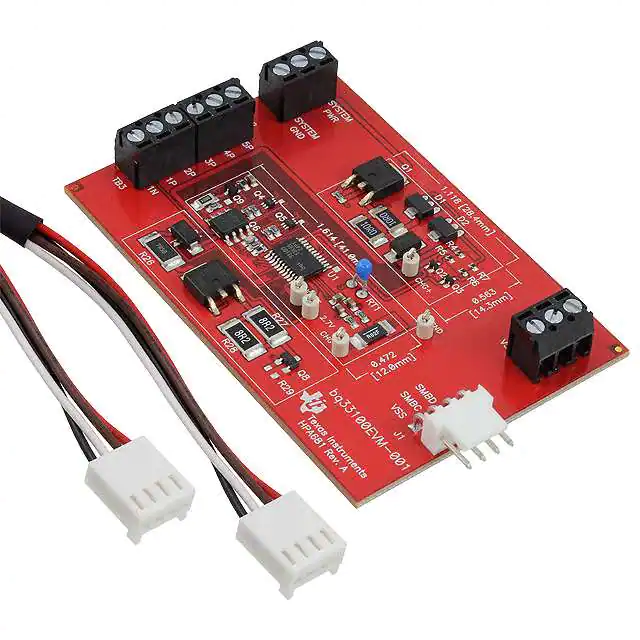
bq33100 Super Capacitor Pack Manager EVM
NOTE: BEFORE YOU START: Download the latest revision of the device firmware and the
evaluation software from the TI bq33100 product page at www.ti.com. Go to the Tools and
Software section. For step-by-step instructions on reprogramming the device firmware, refer
to the application report SLUA336B.
This evaluation module (EVM) is a complete evaluation system for the bq33100 super capacitor manager.
The EVM includes one bq33100 circuit module. An EV2300 PC interface board for gas gauge interface
and a PC USB cable are required for communication with a PC and can be ordered online.
Windows™-based PC software is available online as well. The circuit module includes one bq33100
integrated circuit (IC), charging circuitry, and all other onboard components necessary to monitor and
predict state of health, perform charging, perform cell balancing, monitor critical parameters, and protect
the super capacitors from overvoltage, short-circuit, and overtemperature in 2-, 3-, 4-, or 5-series super
capacitor stacks. The circuit module connects directly across the super capacitor stack. With the EV2300
interface board and software, the user can read the bq33100 data registers, program the chipset for
different stack configurations, log cycling data for further evaluation, and evaluate the overall functionality
of the bq33100 under different conditions.
1
2
3
4
5
6
7
8
9
10
11
Contents
Features ...................................................................................................................... 2
bq33100-Based Circuit Module ........................................................................................... 2
bq33100 Circuit Module Schematic ...................................................................................... 3
Circuit Module Physical Layouts and Bill of Materials .................................................................. 3
EVM Hardware and Software Setup .................................................................................... 12
Troubleshooting Unexpected Dialog Boxes ............................................................................ 12
Hardware Connection ..................................................................................................... 12
Operation ................................................................................................................... 13
Calibration Screen ......................................................................................................... 16
Pro (Advanced) Screen ................................................................................................... 17
Stack Assembly and the bq33100 ....................................................................................... 19
List of Figures
1
2
3
4
5
6
7
8
9
10
11
12
.................................................................................
Top Assembly ...............................................................................................................
Top Layer ....................................................................................................................
Internal Layer 1 ..............................................................................................................
Internal Layer 2 ..............................................................................................................
Bottom Layer ................................................................................................................
Bottom Assembly ...........................................................................................................
Schematic ..................................................................................................................
bq33100 Circuit Module Connection to Cells, System Load, and System Power ................................
SBS Data Screen ..........................................................................................................
Data Flash Screen, Safety Class .......................................................................................
Calibration Screen .........................................................................................................
bq33100EVM-001 Layout (Silk Screen)
4
4
5
5
6
6
7
11
13
14
15
17
Windows is a trademark of Microsoft.
All other trademarks are the property of their respective owners.
SLUU466 – March 2011
Submit Documentation Feedback
bq33100 Super Capacitor Pack Manager EVM
© 2011, Texas Instruments Incorporated
1
�Features
www.ti.com
13
Pro (Advanced) Screen ................................................................................................... 18
14
Connection Sequence
....................................................................................................
19
List of Tables
1
1
Ordering Information ........................................................................................................ 2
2
Common Charging Voltage Configurations for 2-, 3-, 4-, and 5- Cell Monitors ..................................... 3
3
Bill of Materials .............................................................................................................. 8
4
Performance Specification Summary ................................................................................... 12
5
Circuit Module to EV2300 Connections
Complete evaluation system for the bq33100 SBS 1.1-compliant super capacitor management IC
Populated circuit module for quick setup
PC software and interface board for easy evaluation
Software that allows data logging for system analysis
Kit Contents
•
•
1.2
13
Features
•
•
•
•
1.1
................................................................................
bq33100 circuit module
Set of support documentation
Ordering Information
Table 1. Ordering Information
2
EVM PART NUMBER
CHEMISTRY
CONFIGURATION
CAPACITY
bq33100EVM-001
Super Capacitor
2, 3, 4, or 5 cell
Any
bq33100-Based Circuit Module
The bq33100-based circuit module is a complete and compact example solution of a bq33100 circuit for
super capacitor management and protection. The circuit module incorporates a bq33100 battery monitor
IC, charging circuitry and all other components necessary to accurately predict the capacity of 2-, 3-, 4-, or
5-series cells.
2.1
Circuit Module Connections
Contacts on the circuit module provide the following connections:
• Direct connection to the cells: 1N, 1P, 2P, 3P, 4P, 5P
• To the serial communications port (SMBC, SMBD)
• The system load across CAPOUT and VSS
• The system power across System PWR and System GND
• To the fault pin (FAULT)
2
PIN NAME
DESCRIPTION
1N
-ve connection of first (bottom) cap
1P
+ve connection of first (bottom) cap
2P
+ve connection of second cap
3P
+ve connection of third cap
4P
+ve connection of fourth cap
5P
+ve connection of fifth (top) cap
SMBC
Serial communication clock port
SMBD
Serial communication data port
bq33100 Super Capacitor Pack Manager EVM
SLUU466 – March 2011
Submit Documentation Feedback
© 2011, Texas Instruments Incorporated
�bq33100 Circuit Module Schematic
www.ti.com
PIN NAME
3
DESCRIPTION
CAPOUT
System load positive terminal
VSS
System load negative terminal
System PWR
System power positive terminal
System GND
System power negative terminal
FAULT
Fault indicator pin
bq33100 Circuit Module Schematic
This section contains information to consider when changing the cell configuration.
3.1
Schematic
The schematic follows the bill of materials in this user's guide.
3.1.1
Modifications for Changing the Cell Configuration
The bq33100 charger provides the option for changing the 4 voltage levels for various cell configurations.
The default configuration assumes a 5-cell configuration. An adjustment to these voltages will need to be
made for 2-, 3-, or 4- cell configurations. Adjusting the charging levels requires changing out R5, R6, and
R7. See Table 2 for common 2-, 3-, 4-, and 5- cell configurations.
Table 2. Common Charging Voltage Configurations for 2-, 3-, 4-, and 5- Cell Monitors
2-Cell
3-Cell
4-Cell
5-Cell
R4
30kΩ
30kΩ
30kΩ
30kΩ
R5
137kΩ
93.1kΩ
68.1kΩ
57.6kΩ
R6
300kΩ
187kΩ
150kΩ
125kΩ
R7
44.2kΩ
19.6kΩ
12.7kΩ
9.31kΩ
Another modification to consider is to R26. This resistor is used to dissipate extra power in the learn load
circuit. For 4- and 5-cell configurations the resistor should be 7.5 Ω, 2 W. For 2- and 3-cell configurations,
R26 should be removed.
4
Circuit Module Physical Layouts and Bill of Materials
This section contains the board layout, bill of materials, and assembly drawings for the bq33100 circuit
module.
4.1
Board Layout
This section shows the dimensions, PCB layers (Figure 1 through Figure 7), and assembly drawing for the
bq33100 module.
SLUU466 – March 2011
Submit Documentation Feedback
bq33100 Super Capacitor Pack Manager EVM
© 2011, Texas Instruments Incorporated
3
�Circuit Module Physical Layouts and Bill of Materials
www.ti.com
Figure 1. bq33100EVM-001 Layout (Silk Screen)
Figure 2. Top Assembly
4
bq33100 Super Capacitor Pack Manager EVM
© 2011, Texas Instruments Incorporated
SLUU466 – March 2011
Submit Documentation Feedback
�www.ti.com
Circuit Module Physical Layouts and Bill of Materials
Figure 3. Top Layer
Figure 4. Internal Layer 1
SLUU466 – March 2011
Submit Documentation Feedback
bq33100 Super Capacitor Pack Manager EVM
© 2011, Texas Instruments Incorporated
5
�Circuit Module Physical Layouts and Bill of Materials
www.ti.com
Figure 5. Internal Layer 2
Figure 6. Bottom Layer
6
bq33100 Super Capacitor Pack Manager EVM
© 2011, Texas Instruments Incorporated
SLUU466 – March 2011
Submit Documentation Feedback
�www.ti.com
Circuit Module Physical Layouts and Bill of Materials
Figure 7. Bottom Assembly
SLUU466 – March 2011
Submit Documentation Feedback
bq33100 Super Capacitor Pack Manager EVM
© 2011, Texas Instruments Incorporated
7
�Circuit Module Physical Layouts and Bill of Materials
4.2
www.ti.com
Bill of Materials and Schematic
Table 3. Bill of Materials
COUNT
RefDes
Value
Description
SIZE
Part Number
Mfr
9
C1, C2, C3,
C4, C6, C7,
C8, C11, C15
0.1 µF
Capacitor, Ceramic, 50V, X7R, 20%
0603
STD
Any
3
C12, C13, C14 100 pF
Capacitor, Ceramic, 50V, X7R, 10%
0603
STD
Any
3
C5, C9, C10
1.0 µF
Capacitor, Ceramic, 25V, X7R, 20%
0805
STD
Any
2
D1, D2
TL431CPK
IC, Adjustable precision shunt regulator
SOT-89
TL431CPK
TI
2
D3, D4
S1A-13-F
Diode, Glass Passivated Rect. 1A, 50V
SMA
S1A-13-F
Diodes
1
J1
22-05-3041
Header, Friction Lock Ass'y, 4-pin Right Angle
0.400 x 0.500
22-05-3041
Molex
2
Q1, Q7
2SD1758TLR
Transistor, NPN Medium Power, 32V, 2A
SC-63
2SD1758TLR
Rohm
2
Q2, Q3
2SK3019
MOSFET, Nch, 30V, 100mA, 8 Ohm
SC-75A
2SK3019
Rohm
2
Q4, Q5
Si1023X
MOSFET, Pch, -20V, 350mA, 1.2 Ohm
SC-89
Si1023X-T1-E3
Vishay
1
Q6
Si4435DDY
MOSFET, Pch, 30V, 8.0A, 20 milliohm
SOT23
Si4435DDY-T1-E3
Vishay
1
Q8
ZXMN3A14FTA
MOSFET, Nch, 30V, 3.2A, 65 milliOhm
SOT23
ZXMN3A14FTA
Diodes/Zetex
1
Q9
BSS223PW
MOSFET, Pch, -20V, -0.39A, 1.2 Ohm
SOT323
BSS223PW
Infineon
5
R1, R8, R9,
R10, R11
1K
Resistor, Chip, 1/16W, 5%
0603
STD
Any
5
R12, R13,
100
R21, R23, R25
Resistor, Chip, 1/16W, 5%
0603
STD
Any
5
R14, R15,
100
R16, R17, R31
Resistor, Chip, 1/4W, 5%
1206
CRCW1206100RJNEA
Vishay
1
R18
.020 75ppm
Resistor, Chip, 1/2W, 1%, 75ppm
2010
WSL2010R0200FEA
Dale
1
R19
3M
Resistor, Chip, 1/16W, 5%
0603
STD
Any
2
R2, R3
10
Resistor, Chip, 1W, 1%
2010
CRCW201010R0FKEFHP
Vishay/Dale
3
R20, R22, R24 200
Resistor, Chip, 1/16W, 5%
0603
STD
Any
1
R26
7.5
Resistor, Chip, 2W, 1%
2512
RHC2512FT7R50
Stackpole
2
R27, R28
8.2
Resistor, Chip, 1W, 1%
2512
ERJ-1TRQF8R2U
Panasonic - ECG
0
R29
DNP
Resistor, Chip, 1/16W, 5%
0603
STD
Any
1
R30
20K
Resistor, Chip, 1/16W, 5%
0603
STD
Any
1
R32
20K
Resistor, Chip, 1/16W, 1%
0603
STD
Any
1
R33
10K
Resistor, Chip, 1/16W, 1%
0603
STD
Any
1
R4
30.0K
Resistor, Chip, 1/16W, 1%
0402
STD
Any
1
R5
57.6K
Resistor, Chip, 1/16W, 1%
0402
STD
Any
1
R6
124K
Resistor, Chip, 1/16W, 1%
0402
STD
Any
1
R7
9.31K
Resistor, Chip, 1/16W, 1%
0402
STD
Any
8
bq33100 Super Capacitor Pack Manager EVM
SLUU466 – March 2011
Submit Documentation Feedback
© 2011, Texas Instruments Incorporated
�Circuit Module Physical Layouts and Bill of Materials
www.ti.com
Table 3. Bill of Materials (continued)
COUNT
RefDes
Value
Description
SIZE
Part Number
Mfr
1
RT1
10K
Thermistor, 10K Ohm
0.095 x 0.150 inches
103AT-2
Semitec
4
TB1, TB2,
TB3, TB4
ED555/3DS
Terminal Block, 3-pin, 6A, 3.5mm
0.41 x 0.25 inch
ED555/3DS
OST
1
TP1
CHG+
Test Point, White, Thru Hole Color Keyed
0.100 x 0.100 inch
5002
Keystone
1
TP2
CHG-
Test Point, White, Thru Hole Color Keyed
0.100 x 0.100 inch
5002
Keystone
1
TP3
CHGFET
Test Point, White, Thru Hole Color Keyed
0.100 x 0.100 inch
5002
Keystone
1
TP4
2.7V
Test Point, White, Thru Hole Color Keyed
0.100 x 0.100 inch
5002
Keystone
1
TP5
GND
Test Point, White, Thru Hole Color Keyed
0.100 x 0.100 inch
5002
Keystone
1
U1
BQ33100PW
IC, SUPERCAP PACKMANAGER and
PROTECTION
TSSOP-24
BQ33100PW
TI
1
–
PCB
2 x 3 inches
HPA681
Any
Connector
2
J1 mate
Connector, Female, 0.100 Centers
Molex
22-01-3047
8
N/A
Terminals, Crimp, Tin
Molex
08-50-0114
1
N/A
Wire, Insulated 24 Awg, Red, 18 Inches (+/- 3
inches)(USB_5V)
Alpha
1854-3
1
N/A
Wire, Insulated 24 Awg, White, 18 Inches (+/- 3
inches)(SCL)
Alpha
1854-1
1
N/A
Wire, Insulated 24 Awg, Black, 18 Inches (+/- 3
inches)(GND)
Alpha
1854-2
1
N/A
Wire, Insulated 24 Awg, Brown, 18 Inches (+/- 3
inches) (SDA)
Alpha
1854-7
1
N/A
Heatshrink 1"
Any
Any
SLUU466 – March 2011
Submit Documentation Feedback
bq33100 Super Capacitor Pack Manager EVM
© 2011, Texas Instruments Incorporated
9
�Circuit Module Physical Layouts and Bill of Materials
www.ti.com
Table 3. Bill of Materials (continued)
COUNT
RefDes
Value
Description
SIZE
Notes:
1. These assemblies are ESD sensitive, ESD precautions shall be observed.
Part Number
Mfr
2. These assemblies must be clean and free from flux and all contaminants. Use of no clean flux is not acceptable.
3. These assemblies must comply with workmanship standards IPC-A-610 Class 2.
4. Ref designators marked with an asterisk ('**') cannot be substituted. All other components can be substituted with equivalent MFG's components.
5. Make one SMBus connector wire assembly for each assembly produced, from J1 mate, 4 - 24 Awg wires and Crimp terminals. Wire colors for Pin numbers are listed
below. The wire assembly shall have a J1 mate on each end.
Red - Pin # 4 (Signal USB_5V)
Brown - Pin # 3 (Signal SDA)
White - Pin # 2 (Signal SCL)
Black - Pin # 1 (GND)
6. RT1 should be assembled horizontally laying flat against the board Edge.
10
bq33100 Super Capacitor Pack Manager EVM
SLUU466 – March 2011
Submit Documentation Feedback
© 2011, Texas Instruments Incorporated
�Circuit Module Physical Layouts and Bill of Materials
www.ti.com
Figure 8. Schematic
SLUU466 – March 2011
Submit Documentation Feedback
bq33100 Super Capacitor Pack Manager EVM
© 2011, Texas Instruments Incorporated
11
�EVM Hardware and Software Setup
4.3
www.ti.com
bq33100 Circuit Module Performance Specification Summary
Table 4. Performance Specification Summary
Specification
5
Minimum
Typical
Maximum
Units
Input Voltage System PWR to System GND
6
12
15
V
Discharge current
0
2
7
A
EVM Hardware and Software Setup
This section describes how to install the bq33100EVM-001 PC software, and how to connect the different
components of the EVM.
5.1
System Requirements
The bq33100EVSW software requires Windows™ 2000 or Windows XP™. Drivers for Windows 98SE are
provided, but Microsoft™ no longer supports Windows 98 and there may be issues in Windows 98 with
USB driver support. The EV2300 USB drivers have been tested for Windows 98SE, but no assurance is
made for problem-free operation with specific system configurations.
5.2
Software Installation
Get the latest software version in the bq33100 tool folder on www.ti.com, and follow these steps to install
the bq33100 EVSW software:
1. Save the archive to a temporary directory. Open the archive containing the installation package, and
copy its contents to a temporary directory. The executable filename can consist of several component
names and versions. Double-click on the executable filename, and follow the installer instructions to
complete the bq33100 EVM installation.
2. If the EV2300 was not previously installed, after bq33100 EVM installation, a TI USB DRIVER
INSTALLER pops up. Click "Yes" for the agreement message and follow its instructions.
3. Plug the EV2300 into a USB port.
6
Troubleshooting Unexpected Dialog Boxes
Ensure that the files were extracted from the zip file using the Preserve Folder names option.
Ensure that all the files were extracted from the zip file.
The user that is downloading the files must be logged in as the administrator.
The driver is not signed, so the administrator must allow installation of unsigned drivers in the operating
system policy.
7
Hardware Connection
The bq33100EVM-001 comprises three hardware components: the bq33100 circuit module, the EV2300
PC interface board, and the PC.
7.1
Connecting bq33100 Circuit Module to Super Capacitor Stack
Figure 9 shows how to connect the bq33100 circuit module to the super capacitors, system load, and
system power.
The super capacitors should be connected in the following order:
1. 5-Cell Pack: 1N, 1P, 2P, 3P, 4P, and 5P (see Section 2.1 for definitions).
2. 4-Cell Pack: 1N and 1P are connected together, 2P, 3P, 4P, and 5P.
3. 3-Cell Pack: 1N and 1P are connected together, 2P, 3P, and then connect 4P and 5P together.
4. 2-Cell Pack: 1N and 1P are connected together, 2P, and then connect 3P, 4P and 5P together.
12
bq33100 Super Capacitor Pack Manager EVM
© 2011, Texas Instruments Incorporated
SLUU466 – March 2011
Submit Documentation Feedback
�Operation
www.ti.com
Connect the system load between the CAPOUT and VSS terminals. Connect the system power between
the System PWR and System GND terminals.
System
Power
-
+
System PWR
Fault
VSS
System GND
5P
4P TB2
3P
2P
1P TB3
1N
+
CAPOUT
TB4
TB1
-
HPA681
J1
SMBus
Cable
System
Load
SMB
EV2300
Figure 9. bq33100 Circuit Module Connection to Cells, System Load, and System Power
7.2
PC Interface Connection
The following steps configure the hardware for interface to the PC:
1. Connect the bq33100 circuit module to the EV2300 using wire leads as shown in Table 5.
Table 5. Circuit Module to EV2300 Connections
bq33100 Circuit Module
EV2300
SMBD
SMBD
SMBC
SMBC
VSS
GND
2. Connect the PC USB cable to the EV2300 and the PC USB port.
The bq33100EVM-001 is now set up for operation.
8
Operation
This section details the operation of the bq33100 EVSW software.
8.1
Starting the Program
Run bq Evaluation Software from the Start | Programs | Texas Instruments | bq33100 EVSW menu
sequence. The SBS Data screen (Figure 10) appears. Data begins to appear once the (single
time scan) button is clicked, or when the check box is checked. To disable the scan
feature, deselect .
The continuous scanning period can be set via the | Options | and | Set Scan Interval | menu selections.
The range for this interval is 0 ms to 65535 ms. Only items that are selected for scanning are scanned
within this period.
The bq Evaluation Software provides a logging function which logs the values that were last scanned by
EVSW. To enable this function, select the Start Logging button, this causes the Keep Scanning button to
be selected. When logging is Stopped, the keep scanning button is still selected and has to be manually
unchecked.
SLUU466 – March 2011
Submit Documentation Feedback
bq33100 Super Capacitor Pack Manager EVM
© 2011, Texas Instruments Incorporated
13
�Operation
www.ti.com
The logging intervals are specified under the | Options | menu with the maximum value of 65535 ms. The
Log interval cannot be smaller than the Scan interval because this results in the same value being logged
at least twice.
Figure 10. SBS Data Screen
This screen (Figure 10) shows the SBS data set along with additional ManufacturersAccess() command
information such as individual cell measurements. Additional Flag and Static data can be viewed by
selecting the appropriate tab at the bottom of the SBS screen.
Data such as SBS.ManufacturerName( ) is static and does not change. This data is viewed separately
using the Static Data tab available at the bottom of the screen.
Dragging the splitter bar (line that separates the Flags/Static data from SBS values) changes the height of
the Flags/Static Data display. Selecting | View |, then | Auto Arrange | returns the splitter bar to its original
location.
14
bq33100 Super Capacitor Pack Manager EVM
© 2011, Texas Instruments Incorporated
SLUU466 – March 2011
Submit Documentation Feedback
�Operation
www.ti.com
8.2
Setting Programmable bq33100 Options
The bq33100 data flash comes configured per the default settings detailed in the bq33100 data sheet.
Ensure that the settings are correctly changed to match the capacitor stack and application for the
bq33100 solution being evaluated.
IMPORTANT: The correct setting of these options is essential to get the best performance.
The settings can be configured using the Data Flash screen (Figure 11).
Figure 11. Data Flash Screen, Safety Class
To read all the data from the bq33100 data flash, click on menu option | Data Flash | Read All |.
To write to a data flash location, click on the desired location, enter the data and press , which
writes the entire tab of flash data, or select menu option | Data Flash | Write All |. The data flash must be
read before any writes are performed to avoid any incorrect data being written to the device.
The | File | Special Export | menu options allows the data flash to be exported, but it configures the
exported data flash to a learned state ready for mass production use.
The data flash configuration can be saved to a file by selecting | File | Export | and entering a file name. A
data flash file also can be retrieved in this way, imported, and written to the bq33100 using the | Write All |
button.
SLUU466 – March 2011
Submit Documentation Feedback
bq33100 Super Capacitor Pack Manager EVM
© 2011, Texas Instruments Incorporated
15
�Calibration Screen
www.ti.com
The configuration information of the bq33100 and module calibration data also is held in the bq33100 data
flash.
The bq33100 allows for an automatic data flash export function, similar to the SBS Data logging function.
This feature, when selected via | Options | Auto Export |, exports Data Flash to a sequential series of files
named as FilenameNNNNN.gg where N = a decimal number from 0 to 9.
The AutoExport interval is set under the | Options menu | with a minimum value of 15 s. The AutoExport
filename also is set under the | Options menu |.
When a check mark is next to | AutoExport |, the AutoExport is in progress. The same menu selection is
used to turn on / off AutoExport.
If the data flash screen is blank, then the bq33100 that is being used may not be supported by the
bqEVSW version that is being used. An upgrade may be required.
9
Calibration Screen
9.1
How to Calibrate
Before the bq33100 is calibrated:
• Connect 12V to System PWR and System GND inputs
• Connect a load to CAPOUT and VSS that draws approximately 0.5 A and measures discharge current
to use the FET, or
• Connect a current source to 1N and VSS to calibrate without using the FET.
• Measure individual cell stack voltage from 1N, to Cap1(1P), Cap1 + 2(2P), Cap1 + 2 + 3(3P), Cap1 + 2
+ 3 + 4(4P), Cap1 + 2 + 3 + 4 + 5(5P).
• Measure the voltage from the System PWR to System GND inputs
• Measure the temperature of the pack.
These steps may not be required, depending on the type of calibration being performed.
Note that voltage calibration with capacitors attached requires special consideration. Capacitors must be
in a resting state.
9.2
To Calibrate the bq33100
Select the types of calibration to be performed (see Figure 12).
Enter the measured values for the types selected.
If Capacitor Stack Voltage Calibration is selected, then enter the capacitor voltages.
If the load is connected between CAPOUT and VSS-, then select the On (External Load) radio button.
Press the Calibrate Part button.
9.3
System Voltage Calibration
This calibrates the voltage at the VCC pin.
Make sure Capacitor Stack Voltage Calibration has been performed for the pack. If Capacitor Stack
Voltage Calibration is not performed, then System Voltage Calibration calibrates incorrectly.
Remove load/external voltage applied between CAPOUT and VSS.
Check the System Voltage Calibration box, and enter the measured System PWR voltage
Press the Calibrate device as indicated below button to calibrate.
16
bq33100 Super Capacitor Pack Manager EVM
© 2011, Texas Instruments Incorporated
SLUU466 – March 2011
Submit Documentation Feedback
�Pro (Advanced) Screen
www.ti.com
Figure 12. Calibration Screen
10
Pro (Advanced) Screen
10.1 SMB Communication
The set of read/write operations over SMBus are not specific to any gas gauge. These are provided as
general-purpose communication tools (Figure 13).
10.2 Hexadecimal/Decimal Converter
These two boxes convert between hexadecimal and decimal as soon as values are typed into the boxes.
Invalid values may cause erroneous results.
When scaling converted hexadecimal values to a higher number of bytes, follow these rules:
• When unsigned is selected, the left pad contains zeroes.
• When signed is selected, the left pad contains zeroes for a positive number, or the left pad contains F for
negative numbers.
SLUU466 – March 2011
Submit Documentation Feedback
bq33100 Super Capacitor Pack Manager EVM
© 2011, Texas Instruments Incorporated
17
�Pro (Advanced) Screen
www.ti.com
10.3 Programming
This screen allows device reprogramming from unencrypted and encrypted files.
Figure 13. Pro (Advanced) Screen
18
bq33100 Super Capacitor Pack Manager EVM
© 2011, Texas Instruments Incorporated
SLUU466 – March 2011
Submit Documentation Feedback
�Stack Assembly and the bq33100
www.ti.com
11
Stack Assembly and the bq33100
This section describes a recommended assembly sequence for a bq33100-based super capacitor stack.
This procedure results in the most time-efficient setup of the super capacitor stack. Following are the
steps for connecting a 5-series capacitor stack to the bq33100EVM board.
5P
4P
+
-
CAP 5
3P
+
-
CAP 4
2P
+
-
CAP 3
1P
+
-
1N
+
CAP 2
-
EVM
Connector
Capacitor
Stack
CAP 1
Figure 14. Connection Sequence
1. Connect the most negative terminal (– terminal of cap 1) of the serially-connected, 5-capacitor stack to
the 1N PIN of the TB2–TB3 connector as shown in Figure 14. (See also Figure 9 for TB2–TB3
location).
2. Connect the positive terminal of cell 1 to 1P.
3. Connect the positive terminal of cell 2 to 2P.
4. Connect the positive terminal of cell 3 to 3P.
5. Connect the positive terminal of cell 4 to 4P.
6. Connect the positive terminal of the capacitor stack (+) to 5P.
7. Connect external power (from 6 V to 15 V) to the System PWR and System GND terminals to wake up
the EVM from shutdown mode.
8. Connect the SMBus connector (J1) to the EV2300 adapter and start the EV software.
9. Navigate to the Flash Screen. Change the flash constants that correspond to the specific parameters
of your application (see the data sheet). For the first evaluation, the default values may be used.
10. Navigate to the Calibration screen. Select the check-box for software voltage calibration near
Measured voltage field. Measure between 1P and 1N for capacitor 1, 2P and 1N for capacitors 1 + 2,
3P and 1N for capacitors 1 + 2 + 3, 4P and 1N for capacitors 1 + 2 + 3 + 4, 5P and 1N for capacitors 1
+ 2 + 3 + 4 + 5 and enter the values into the Enter actual voltage field. Click the calibrate part button.
11. Now the pack is ready and charge/discharge tests can be conducted.
SLUU466 – March 2011
Submit Documentation Feedback
bq33100 Super Capacitor Pack Manager EVM
© 2011, Texas Instruments Incorporated
19
�Evaluation Board/Kit Important Notice
Texas Instruments (TI) provides the enclosed product(s) under the following conditions:
This evaluation board/kit is intended for use for ENGINEERING DEVELOPMENT, DEMONSTRATION, OR EVALUATION
PURPOSES ONLY and is not considered by TI to be a finished end-product fit for general consumer use. Persons handling the
product(s) must have electronics training and observe good engineering practice standards. As such, the goods being provided are
not intended to be complete in terms of required design-, marketing-, and/or manufacturing-related protective considerations,
including product safety and environmental measures typically found in end products that incorporate such semiconductor
components or circuit boards. This evaluation board/kit does not fall within the scope of the European Union directives regarding
electromagnetic compatibility, restricted substances (RoHS), recycling (WEEE), FCC, CE or UL, and therefore may not meet the
technical requirements of these directives or other related directives.
Should this evaluation board/kit not meet the specifications indicated in the User’s Guide, the board/kit may be returned within 30
days from the date of delivery for a full refund. THE FOREGOING WARRANTY IS THE EXCLUSIVE WARRANTY MADE BY
SELLER TO BUYER AND IS IN LIEU OF ALL OTHER WARRANTIES, EXPRESSED, IMPLIED, OR STATUTORY, INCLUDING
ANY WARRANTY OF MERCHANTABILITY OR FITNESS FOR ANY PARTICULAR PURPOSE.
The user assumes all responsibility and liability for proper and safe handling of the goods. Further, the user indemnifies TI from all
claims arising from the handling or use of the goods. Due to the open construction of the product, it is the user’s responsibility to
take any and all appropriate precautions with regard to electrostatic discharge.
EXCEPT TO THE EXTENT OF THE INDEMNITY SET FORTH ABOVE, NEITHER PARTY SHALL BE LIABLE TO THE OTHER
FOR ANY INDIRECT, SPECIAL, INCIDENTAL, OR CONSEQUENTIAL DAMAGES.
TI currently deals with a variety of customers for products, and therefore our arrangement with the user is not exclusive.
TI assumes no liability for applications assistance, customer product design, software performance, or infringement of
patents or services described herein.
Please read the User’s Guide and, specifically, the Warnings and Restrictions notice in the User’s Guide prior to handling the
product. This notice contains important safety information about temperatures and voltages. For additional information on TI’s
environmental and/or safety programs, please contact the TI application engineer or visit www.ti.com/esh.
No license is granted under any patent right or other intellectual property right of TI covering or relating to any machine, process, or
combination in which such TI products or services might be or are used.
FCC Warning
This evaluation board/kit is intended for use for ENGINEERING DEVELOPMENT, DEMONSTRATION, OR EVALUATION
PURPOSES ONLY and is not considered by TI to be a finished end-product fit for general consumer use. It generates, uses, and
can radiate radio frequency energy and has not been tested for compliance with the limits of computing devices pursuant to part 15
of FCC rules, which are designed to provide reasonable protection against radio frequency interference. Operation of this
equipment in other environments may cause interference with radio communications, in which case the user at his own expense
will be required to take whatever measures may be required to correct this interference.
EVM Warnings and Restrictions
It is important to operate this EVM within the input voltage range of 6 V to 15 V and the output voltage range of 0 V to 16.4 V .
Exceeding the specified input range may cause unexpected operation and/or irreversible damage to the EVM. If there are
questions concerning the input range, please contact a TI field representative prior to connecting the input power.
Applying loads outside of the specified output range may result in unintended operation and/or possible permanent damage to the
EVM. Please consult the EVM User's Guide prior to connecting any load to the EVM output. If there is uncertainty as to the load
specification, please contact a TI field representative.
During normal operation, some circuit components may have case temperatures greater than 60°C. The EVM is designed to
operate properly with certain components above 60°C as long as the input and output ranges are maintained. These components
include but are not limited to linear regulators, switching transistors, pass transistors, and current sense resistors. These types of
devices can be identified using the EVM schematic located in the EVM User's Guide. When placing measurement probes near
these devices during operation, please be aware that these devices may be very warm to the touch.
Mailing Address: Texas Instruments, Post Office Box 655303, Dallas, Texas 75265
Copyright © 2011, Texas Instruments Incorporated
�IMPORTANT NOTICE
Texas Instruments Incorporated and its subsidiaries (TI) reserve the right to make corrections, modifications, enhancements, improvements,
and other changes to its products and services at any time and to discontinue any product or service without notice. Customers should
obtain the latest relevant information before placing orders and should verify that such information is current and complete. All products are
sold subject to TI’s terms and conditions of sale supplied at the time of order acknowledgment.
TI warrants performance of its hardware products to the specifications applicable at the time of sale in accordance with TI’s standard
warranty. Testing and other quality control techniques are used to the extent TI deems necessary to support this warranty. Except where
mandated by government requirements, testing of all parameters of each product is not necessarily performed.
TI assumes no liability for applications assistance or customer product design. Customers are responsible for their products and
applications using TI components. To minimize the risks associated with customer products and applications, customers should provide
adequate design and operating safeguards.
TI does not warrant or represent that any license, either express or implied, is granted under any TI patent right, copyright, mask work right,
or other TI intellectual property right relating to any combination, machine, or process in which TI products or services are used. Information
published by TI regarding third-party products or services does not constitute a license from TI to use such products or services or a
warranty or endorsement thereof. Use of such information may require a license from a third party under the patents or other intellectual
property of the third party, or a license from TI under the patents or other intellectual property of TI.
Reproduction of TI information in TI data books or data sheets is permissible only if reproduction is without alteration and is accompanied
by all associated warranties, conditions, limitations, and notices. Reproduction of this information with alteration is an unfair and deceptive
business practice. TI is not responsible or liable for such altered documentation. Information of third parties may be subject to additional
restrictions.
Resale of TI products or services with statements different from or beyond the parameters stated by TI for that product or service voids all
express and any implied warranties for the associated TI product or service and is an unfair and deceptive business practice. TI is not
responsible or liable for any such statements.
TI products are not authorized for use in safety-critical applications (such as life support) where a failure of the TI product would reasonably
be expected to cause severe personal injury or death, unless officers of the parties have executed an agreement specifically governing
such use. Buyers represent that they have all necessary expertise in the safety and regulatory ramifications of their applications, and
acknowledge and agree that they are solely responsible for all legal, regulatory and safety-related requirements concerning their products
and any use of TI products in such safety-critical applications, notwithstanding any applications-related information or support that may be
provided by TI. Further, Buyers must fully indemnify TI and its representatives against any damages arising out of the use of TI products in
such safety-critical applications.
TI products are neither designed nor intended for use in military/aerospace applications or environments unless the TI products are
specifically designated by TI as military-grade or "enhanced plastic." Only products designated by TI as military-grade meet military
specifications. Buyers acknowledge and agree that any such use of TI products which TI has not designated as military-grade is solely at
the Buyer's risk, and that they are solely responsible for compliance with all legal and regulatory requirements in connection with such use.
TI products are neither designed nor intended for use in automotive applications or environments unless the specific TI products are
designated by TI as compliant with ISO/TS 16949 requirements. Buyers acknowledge and agree that, if they use any non-designated
products in automotive applications, TI will not be responsible for any failure to meet such requirements.
Following are URLs where you can obtain information on other Texas Instruments products and application solutions:
Products
Applications
Audio
www.ti.com/audio
Communications and Telecom www.ti.com/communications
Amplifiers
amplifier.ti.com
Computers and Peripherals
www.ti.com/computers
Data Converters
dataconverter.ti.com
Consumer Electronics
www.ti.com/consumer-apps
DLP® Products
www.dlp.com
Energy and Lighting
www.ti.com/energy
DSP
dsp.ti.com
Industrial
www.ti.com/industrial
Clocks and Timers
www.ti.com/clocks
Medical
www.ti.com/medical
Interface
interface.ti.com
Security
www.ti.com/security
Logic
logic.ti.com
Space, Avionics and Defense
www.ti.com/space-avionics-defense
Power Mgmt
power.ti.com
Transportation and
Automotive
www.ti.com/automotive
Microcontrollers
microcontroller.ti.com
Video and Imaging
www.ti.com/video
RFID
www.ti-rfid.com
Wireless
www.ti.com/wireless-apps
RF/IF and ZigBee® Solutions
www.ti.com/lprf
TI E2E Community Home Page
e2e.ti.com
Mailing Address: Texas Instruments, Post Office Box 655303, Dallas, Texas 75265
Copyright © 2011, Texas Instruments Incorporated
�