bq4014/bq4014Y
256Kx8 Nonvolatile SRAM
Features
General Description
➤ Data retention in the absence of
power
The CMOS bq4014 is a nonvolatile
2,097,152-bit static RAM organized as
262,144 words by 8 bits. The integral
control circuitry and lithium energy
source provide reliable nonvolatility
coupled with the unlimited write
cycles of standard SRAM.
➤ Automatic write-protection
during power-up/power-down
cycles
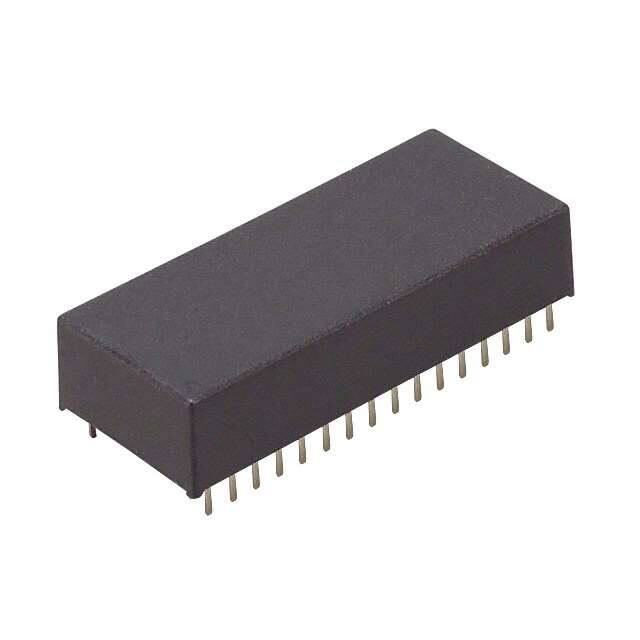
➤ Industry-standard 32-pin 256K x
8 pinout
➤ Conventional SRAM operation;
unlimited write cycles
➤ 10-year minimum data retention
in absence of power
➤ Battery internally isolated until
power is applied
Pin Connections
The control circuitry constantly
monitors the single 5V supply for an
out-of-tolerance condition. When
VCC falls out of tolerance, the SRAM
is unconditionally write-protected to
prevent inadvertent write operation.
At this time the integral energy
Pin Names
source is switched on to sustain the
memory until after VCC returns
valid.
The bq4014 uses extremely low
standby current CMOS SRAMs,
coupled with small lithium coin
cells to provide nonvolatility without
long write-cycle times and the writecycle limitations associated with
EEPROM.
The bq4014 requires no external circuitry and is compatible with the
industry-standard 2Mb SRAM
pinout.
Block Diagram
A0–A17
Address inputs
DQ0–DQ7
Data input/output
CE
Chip enable input
OE
Output enable input
WE
Write enable input
NC
No connect
VCC
+5 volt supply input
VSS
Ground
Selection Guide
Maximum
Access
Time (ns)
Negative
Supply
Tolerance
bq4014 -85
85
-5%
bq4014 -120
120
-5%
Part
Number
Maximum
Access
Time (ns)
Negative
Supply
Tolerance
bq4014Y -85
85
-10%
bq4014Y -120
120
-10%
Part
Number
Sept. 1992
1
�bq4014/bq4014Y
As VCC falls past VPFD and approaches 3V, the control
circuitry switches to the internal lithium backup supply,
which provides data retention until valid VCC is applied.
Functional Description
When power is valid, the bq4014 operates as a standard
CMOS SRAM. During power-down and power-up cycles,
the bq4014 acts as a nonvolatile memory, automatically
protecting and preserving the memory contents.
When VCC returns to a level above the internal backup
cell voltage, the supply is switched back to VCC. After
VCC ramps above the VPFD threshold, write-protection
continues for a time tCER (120ms maximum) to allow for
processor stabilization. Normal memory operation may
resume after this time.
Power-down/power-up control circuitry constantly
monitors the VCC supply for a power-fail-detect threshold
VPFD. The bq4014 monitors for VPFD = 4.62V typical for
use in systems with 5% supply tolerance. The bq4014Y
monitors for VPFD = 4.37V typical for use in systems with
10% supply tolerance.
The internal coin cells used by the bq4014 have an
extremely long shelf life and provide data retention for
more than 10 years in the absence of system power.
When VCC falls below the VPFD threshold, the SRAM
automatically write-protects the data. All outputs
become high impedance, and all inputs are treated as
“don’t care.” If a valid access is in process at the time of
power-fail detection, the memory cycle continues to completion. If the memory cycle fails to terminate within
time tWPT, write-protection takes place.
As shipped from Benchmarq, the integral lithium cells
are electrically isolated from the memory. (Self-discharge
in this condition is approximately 0.5% per year.)
Following the first application of VCC, this isolation is
broken, and the lithium backup provides data retention
on subsequent power-downs.
Truth Table
Mode
CE
WE
OE
I/O Operation
Power
Not selected
H
X
X
High Z
Standby
Output disable
L
H
H
High Z
Active
Read
L
H
L
DOUT
Active
Write
L
L
X
DIN
Active
Absolute Maximum Ratings
Value
Unit
VCC
Symbol
DC voltage applied on VCC relative to VSS
-0.3 to 7.0
V
VT
DC voltage applied on any pin excluding VCC
relative to VSS
-0.3 to 7.0
V
TOPR
Operating temperature
0 to +70
°C
TSTG
Storage temperature
-40 to +70
°C
TBIAS
Temperature under bias
-10 to +70
°C
TSOLDER
Soldering temperature
+260
°C
Note:
Parameter
Conditions
VT ≤ VCC + 0.3
For 10 seconds
Permanent device damage may occur if Absolute Maximum Ratings are exceeded. Functional operation
should be limited to the Recommended DC Operating Conditions detailed in this data sheet. Exposure to
conditions beyond the operational limits for extended periods of time may affect device reliability.
Sept. 1992
2
�bq4014/bq4014Y
Recommended DC Operating Conditions (TA = 0 to 70°C)
Symbol
Parameter
Minimum
Typical
Maximum
Unit
4.5
5.0
5.5
V
bq4014Y
4.75
5.0
5.5
V
bq4014
0
0
0
V
VCC
Supply voltage
VSS
Supply voltage
VIL
Input low voltage
-0.3
-
0.8
V
VIH
Input high voltage
2.2
-
VCC + 0.3
V
Note:
Typical values indicate operation at TA = 25°C.
DC Electrical Characteristics (TA = 0 to 70°C, VCCmin
Symbol
Notes
Parameter
≤ VCC ≤ VCCmax)
Minimum
Typical
Maximum
Unit
Conditions/Notes
ILI
Input leakage current
-
-
±2
µA
VIN = VSS to VCC
ILO
Output leakage current
-
-
±2
µA
CE = VIH or OE = VIH or
WE = VIL
VOH
Output high voltage
2.4
-
-
V
IOH = -1.0 mA
VOL
Output low voltage
-
-
0.4
V
IOL = 2.1 mA
ISB1
Standby supply current
-
5
12
mA
CE = VIH
ISB2
Standby supply current
-
2.5
5
mA
CE ≥ VCC - 0.2V,
0V ≤ VIN ≤ 0.2V,
or VIN ≥ VCC - 0.2
ICC
Operating supply current
-
75
110
mA
Min. cycle, duty = 100%,
CE = VIL, II/O = 0mAV,
A17 < VIL or A17 > VIH
4.55
4.62
4.75
V
bq4014
VPFD
Power-fail-detect voltage
4.30
4.37
4.50
V
bq4014Y
VSO
Supply switch-over voltage
-
3
-
V
Note:
Typical values indicate operation at TA = 25°C, VCC = 5V.
Capacitance (TA = 25°C, F = 1MHz, VCC = 5.0V)
Minimum
Typical
Maximum
Unit
CI/O
Symbol
Input/output capacitance
-
-
40
pF
Output voltage = 0V
CIN
Input capacitance
-
-
40
pF
Input voltage = 0V
Note:
Parameter
These parameters are sampled and not 100% tested.
Sept. 1992
3
Conditions
�bq4014/bq4014Y
AC Test Conditions
Parameter
Test Conditions
Input pulse levels
0V to 3.0V
Input rise and fall times
5 ns
Input and output timing reference levels
1.5 V (unless otherwise specified)
Output load (including scope and jig)
See Figures 1 and 2
Figure 1. Output Load A
Read Cycle
Figure 2. Output Load B
(TA = 0 to 70°C, VCCmin ≤ VCC ≤ VCCmax)
-120
-85
Symbol
Parameter
Min.
Max.
Min.
Max.
Unit
85
-
120
-
ns
Conditions
tRC
Read cycle time
tAA
Address access time
-
85
-
120
ns
Output load A
tACE
Chip enable access time
-
85
-
120
ns
Output load A
tOE
Output enable to output valid
-
45
-
60
ns
Output load A
tCLZ
Chip enable to output in low Z
5
-
5
-
ns
Output load B
tOLZ
Output enable to output in low Z
0
-
0
-
ns
Output load B
tCHZ
Chip disable to output in high Z
0
35
0
45
ns
Output load B
tOHZ
Output disable to output in high Z
0
25
0
35
ns
Output load B
tOH
Output hold from address change
10
-
10
-
ns
Output load A
Sept. 1992
4
�bq4014/bq4014Y
Read Cycle No. 1 (Address Access) 1,2
Read Cycle No. 2 (CE Access) 1,3,4
Read Cycle No. 3 (OE Access) 1,5
Notes:
1. WE is held high for a read cycle.
2. Device is continuously selected: CE = OE = VIL.
3. Address is valid prior to or coincident with CE transition low.
4. OE = VIL.
5. Device is continuously selected: CE = VIL.
Sept. 1992
5
�bq4014/bq4014Y
Write Cycle
(TA = 0 to 70°C, VCCmin ≤ VCC ≤ VCCmax)
-120
-85
Symbol
Parameter
Min.
Max.
Min.
Max. Units
Conditions/Notes
tWC
Write cycle time
85
-
120
-
ns
tCW
Chip enable to end of write
75
-
100
-
ns
(1)
tAW
Address valid to end of write
75
-
100
-
ns
(1)
tAS
Address setup time
0
-
0
-
ns
Measured from address valid to
beginning of write. (2)
tWP
Write pulse width
65
-
85
-
ns
Measured from beginning of write to
end of write. (1)
tWR1
Write recovery time
(write cycle 1)
5
-
5
-
ns
Measured from WE going high to end
of write cycle. (3)
tWR2
Write recovery time
(write cycle 2)
15
-
15
-
ns
Measured from CE going high to end
of write cycle. (3)
tDW
Data valid to end of write
35
-
45
-
ns
Measured to first low-to-high
transition of either CE or WE.
tDH1
Data hold time
(write cycle 1)
0
-
0
-
ns
Measured from WE going high to end
of write cycle. (4)
tDH2
Data hold time
(write cycle 2)
10
-
10
-
ns
Measured from CE going high to end
of write cycle. (4)
tWZ
Write enabled to output in
high Z
0
30
0
40
ns
I/O pins are in output state. (5)
tOW
Output active from end of
write
0
-
0
-
ns
I/O pins are in output state. (5)
Notes:
1. A write ends at the earlier transition of CE going high and WE going high.
2. A write occurs during the overlap of a low CE and a low WE. A write begins at the later transition
of CE going low and WE going low.
3. Either tWR1 or tWR2 must be met.
4. Either tDH1 or tDH2 must be met.
5. If CE goes low simultaneously with WE going low or after WE going low, the outputs remain in
high-impedance state.
Sept. 1992
6
�bq4014/bq4014Y
Write Cycle No. 1 (WE-Controlled) 1,2,3
Write Cycle No. 2 (CE-Controlled) 1,2,3,4,5
Notes:
1. CE or WE must be high during address transition.
2. Because I/O may be active (OE low) during this period, data input signals of opposite polarity to the
outputs must not be applied.
3. If OE is high, the I/O pins remain in a state of high impedance.
4. Either tWR1 or tWR2 must be met.
5. Either tDH1 or tDH2 must be met.
Sept. 1992
7
�bq4014/bq4014Y
Power-Down/Power-Up Cycle (TA = 0 to 70°C)
Symbol
Parameter
Minimum
Typical
Maximum
Unit
tPF
VCC slew, 4.75 to 4.25 V
300
-
-
µs
tFS
VCC slew, 4.25 to VSO
10
-
-
µs
tPU
VCC slew, VSO to VPFD (max.)
0
-
-
µs
tCER
Chip enable recovery time
40
80
120
ms
tDR
Data-retention time in
absence of VCC
10
-
-
years
tWPT
Write-protect time
40
100
150
µs
Notes:
Conditions
Time during which
SRAM is write-protected
after VCC passes VPFD on
power-up.
TA = 25°C. (2)
Delay after VCC slews
down past VPFD before
SRAM is write-protected.
1. Typical values indicate operation at TA = 25°C, VCC = 5V.
2. Batteries are disconnected from circuit until after VCC is applied for the first time. tDR is the
accumulated time in absence of power beginning when power is first applied to the device.
Caution: Negative undershoots below the absolute maximum rating of -0.3V in battery-backup mode
may affect data integrity.
Power-Down/Power-Up Timing
Sept. 1992
8
�bq4014/bq4014Y
Data Sheet Revision History (Sept. 1992 Changes From Sept. 1990)
Clarification of ICC test conditions, page 3.
MB: 32-Pin B-Type Module
32-Pin MB (B-Type Module)
Dimension
Minimum
Maximum
A
A1
B
0.365
0.015
0.017
0.375
0.023
C
D
E
e
0.008
2.070
0.710
0.590
0.013
2.100
0.740
0.630
G
0.090
L
0.120
S
0.275
All dimensions are in inches.
Sept. 1992
9
0.110
0.150
0.310
�bq4014/bq4014Y
Ordering Information
bq4014
MB Temperature:
blank = Commercial (0 to +70°C)
Speed Options:
85 = 85 ns
120 = 120 ns
Package Option:
MB = B-type module
Supply Tolerance:
no mark = 5% negative supply tolerance
Y = 10% negative supply tolerance
Device:
bq4014
256K x 8 NVSRAM
Sept. 1992
10
�PACKAGE OPTION ADDENDUM
www.ti.com
5-Feb-2014
PACKAGING INFORMATION
Orderable Device
Status
(1)
Package Type Package Pins Package
Drawing
Qty
Eco Plan
Lead/Ball Finish
MSL Peak Temp
(2)
(6)
(3)
Op Temp (°C)
(4/5)
BQ4014MB-120
OBSOLETE DIP MODULE
MB
32
TBD
Call TI
Call TI
0 to 70
BQ4014MB-85
OBSOLETE DIP MODULE
MB
32
TBD
Call TI
Call TI
0 to 70
LIFEBUY DIP MODULE
MB
32
TBD
Call TI
Call TI
0 to 70
BQ4014YMB-85
Device Marking
(1)
The marketing status values are defined as follows:
ACTIVE: Product device recommended for new designs.
LIFEBUY: TI has announced that the device will be discontinued, and a lifetime-buy period is in effect.
NRND: Not recommended for new designs. Device is in production to support existing customers, but TI does not recommend using this part in a new design.
PREVIEW: Device has been announced but is not in production. Samples may or may not be available.
OBSOLETE: TI has discontinued the production of the device.
(2)
Eco Plan - The planned eco-friendly classification: Pb-Free (RoHS), Pb-Free (RoHS Exempt), or Green (RoHS & no Sb/Br) - please check http://www.ti.com/productcontent for the latest availability
information and additional product content details.
TBD: The Pb-Free/Green conversion plan has not been defined.
Pb-Free (RoHS): TI's terms "Lead-Free" or "Pb-Free" mean semiconductor products that are compatible with the current RoHS requirements for all 6 substances, including the requirement that
lead not exceed 0.1% by weight in homogeneous materials. Where designed to be soldered at high temperatures, TI Pb-Free products are suitable for use in specified lead-free processes.
Pb-Free (RoHS Exempt): This component has a RoHS exemption for either 1) lead-based flip-chip solder bumps used between the die and package, or 2) lead-based die adhesive used between
the die and leadframe. The component is otherwise considered Pb-Free (RoHS compatible) as defined above.
Green (RoHS & no Sb/Br): TI defines "Green" to mean Pb-Free (RoHS compatible), and free of Bromine (Br) and Antimony (Sb) based flame retardants (Br or Sb do not exceed 0.1% by weight
in homogeneous material)
(3)
MSL, Peak Temp. - The Moisture Sensitivity Level rating according to the JEDEC industry standard classifications, and peak solder temperature.
(4)
There may be additional marking, which relates to the logo, the lot trace code information, or the environmental category on the device.
(5)
Multiple Device Markings will be inside parentheses. Only one Device Marking contained in parentheses and separated by a "~" will appear on a device. If a line is indented then it is a continuation
of the previous line and the two combined represent the entire Device Marking for that device.
(6)
Lead/Ball Finish - Orderable Devices may have multiple material finish options. Finish options are separated by a vertical ruled line. Lead/Ball Finish values may wrap to two lines if the finish
value exceeds the maximum column width.
Important Information and Disclaimer:The information provided on this page represents TI's knowledge and belief as of the date that it is provided. TI bases its knowledge and belief on information
provided by third parties, and makes no representation or warranty as to the accuracy of such information. Efforts are underway to better integrate information from third parties. TI has taken and
continues to take reasonable steps to provide representative and accurate information but may not have conducted destructive testing or chemical analysis on incoming materials and chemicals.
TI and TI suppliers consider certain information to be proprietary, and thus CAS numbers and other limited information may not be available for release.
Addendum-Page 1
Samples
�PACKAGE OPTION ADDENDUM
www.ti.com
5-Feb-2014
In no event shall TI's liability arising out of such information exceed the total purchase price of the TI part(s) at issue in this document sold by TI to Customer on an annual basis.
Addendum-Page 2
�MECHANICAL DATA
MPDI062 – MAY 2001
MB (R-PDIP-T32)
PLASTIC DUAL-IN-LINE
Millimeters
Inches
Dimension
Min.
Max.
Min.
Max.
A
0.365
0.375
9.27
A1
0.015
–
0.38
9.53
–
B
0.017
0.023
0.43
0.58
C
0.008
0.013
0.20
0.33
D
2.070
2.100
52.58
53.34
E
0.710
0.740
18.03
18.80
e
G
0.590
0.630
14.99
16.00
0.090
0.110
2.29
2.79
L
0.120
0.150
3.05
3.81
S
0.275
0.310
6.99
7.87
D
E
A
L
A1
C
B
e
S
G
4201976/A 03/01
NOTES: A. All linear dimensions are in inches (mm).
B. This drawing is subject to change without notice.
•
POST OFFICE BOX 655303 DALLAS, TEXAS 75265
POST OFFICE BOX 1443 HOUSTON, TEXAS 77251–1443
•
1
�IMPORTANT NOTICE
Texas Instruments Incorporated and its subsidiaries (TI) reserve the right to make corrections, enhancements, improvements and other
changes to its semiconductor products and services per JESD46, latest issue, and to discontinue any product or service per JESD48, latest
issue. Buyers should obtain the latest relevant information before placing orders and should verify that such information is current and
complete. All semiconductor products (also referred to herein as “components”) are sold subject to TI’s terms and conditions of sale
supplied at the time of order acknowledgment.
TI warrants performance of its components to the specifications applicable at the time of sale, in accordance with the warranty in TI’s terms
and conditions of sale of semiconductor products. Testing and other quality control techniques are used to the extent TI deems necessary
to support this warranty. Except where mandated by applicable law, testing of all parameters of each component is not necessarily
performed.
TI assumes no liability for applications assistance or the design of Buyers’ products. Buyers are responsible for their products and
applications using TI components. To minimize the risks associated with Buyers’ products and applications, Buyers should provide
adequate design and operating safeguards.
TI does not warrant or represent that any license, either express or implied, is granted under any patent right, copyright, mask work right, or
other intellectual property right relating to any combination, machine, or process in which TI components or services are used. Information
published by TI regarding third-party products or services does not constitute a license to use such products or services or a warranty or
endorsement thereof. Use of such information may require a license from a third party under the patents or other intellectual property of the
third party, or a license from TI under the patents or other intellectual property of TI.
Reproduction of significant portions of TI information in TI data books or data sheets is permissible only if reproduction is without alteration
and is accompanied by all associated warranties, conditions, limitations, and notices. TI is not responsible or liable for such altered
documentation. Information of third parties may be subject to additional restrictions.
Resale of TI components or services with statements different from or beyond the parameters stated by TI for that component or service
voids all express and any implied warranties for the associated TI component or service and is an unfair and deceptive business practice.
TI is not responsible or liable for any such statements.
Buyer acknowledges and agrees that it is solely responsible for compliance with all legal, regulatory and safety-related requirements
concerning its products, and any use of TI components in its applications, notwithstanding any applications-related information or support
that may be provided by TI. Buyer represents and agrees that it has all the necessary expertise to create and implement safeguards which
anticipate dangerous consequences of failures, monitor failures and their consequences, lessen the likelihood of failures that might cause
harm and take appropriate remedial actions. Buyer will fully indemnify TI and its representatives against any damages arising out of the use
of any TI components in safety-critical applications.
In some cases, TI components may be promoted specifically to facilitate safety-related applications. With such components, TI’s goal is to
help enable customers to design and create their own end-product solutions that meet applicable functional safety standards and
requirements. Nonetheless, such components are subject to these terms.
No TI components are authorized for use in FDA Class III (or similar life-critical medical equipment) unless authorized officers of the parties
have executed a special agreement specifically governing such use.
Only those TI components which TI has specifically designated as military grade or “enhanced plastic” are designed and intended for use in
military/aerospace applications or environments. Buyer acknowledges and agrees that any military or aerospace use of TI components
which have not been so designated is solely at the Buyer's risk, and that Buyer is solely responsible for compliance with all legal and
regulatory requirements in connection with such use.
TI has specifically designated certain components as meeting ISO/TS16949 requirements, mainly for automotive use. In any case of use of
non-designated products, TI will not be responsible for any failure to meet ISO/TS16949.
Products
Applications
Audio
www.ti.com/audio
Automotive and Transportation
www.ti.com/automotive
Amplifiers
amplifier.ti.com
Communications and Telecom
www.ti.com/communications
Data Converters
dataconverter.ti.com
Computers and Peripherals
www.ti.com/computers
DLP® Products
www.dlp.com
Consumer Electronics
www.ti.com/consumer-apps
DSP
dsp.ti.com
Energy and Lighting
www.ti.com/energy
Clocks and Timers
www.ti.com/clocks
Industrial
www.ti.com/industrial
Interface
interface.ti.com
Medical
www.ti.com/medical
Logic
logic.ti.com
Security
www.ti.com/security
Power Mgmt
power.ti.com
Space, Avionics and Defense
www.ti.com/space-avionics-defense
Microcontrollers
microcontroller.ti.com
Video and Imaging
www.ti.com/video
RFID
www.ti-rfid.com
OMAP Applications Processors
www.ti.com/omap
TI E2E Community
e2e.ti.com
Wireless Connectivity
www.ti.com/wirelessconnectivity
Mailing Address: Texas Instruments, Post Office Box 655303, Dallas, Texas 75265
Copyright © 2014, Texas Instruments Incorporated
�