bq4842Y
RTC Module With 128Kx8 NVSRAM
Features
General Description
➤ Integrated SRAM, real-time
clock, CPU supervisor, crystal,
power-fail control circuit, and
battery
The bq4842Y RTC Module is a nonvolatile 1,048,576-bit SRAM organized as 131,072 words by 8 bits with
an integral accessible real-time
clock and CPU supervisor. The CPU
supervisor provides a programmable
watchdog timer and a microprocessor reset. Other features include
alarm, power-fail, and periodic interrupts, and a battery-low warning.
➤ Real-Time Clock counts hundredths of seconds through years
in BCD format
➤ RAM-like clock access
➤ Compatible with industrystandard 128K x 8 SRAMs
➤ Unlimited write cycles
➤ 10-year minimum data retention
and clock operation in the absence of power
➤ Automatic power-fail chip deselect and write-protection
➤ Watchdog timer, power-on reset,
alarm/periodic interrupt, powerfail and battery-low warning
The device combines an internal
lithium battery, quartz crystal, clock
and power-fail chip, and a full
CMOS SRAM in a plastic 32-pin
DIP module. The RTC Module directly replaces industry-standard
SRAMs and also fits into many
EPR O M a n d E E P R O M s o ck e ts
without any requirement for special
write timing or limitations on the
number of write cycles.
Registers for the real-time clock,
alarm and other special functions
are located in registers 1FFF0h–
1FFFFh of the memory array.
The clock and alarm registers are
dual-port read/write SRAM locations that are updated once per second by a clock control circuit from
the internal clock counters. The
dual-port registers allow clock updates to occur without interrupting
normal access to the rest of the
SRAM array.
The bq4842Y also contains a powerfail-detect circuit. The circuit deselects the device whenever VCC falls
below tolerance, providing a high degree of data security. The battery is
electrically isolated when shipped
from the factory to provide maximum battery capacity. The battery
remains disconnected until the first
application of VCC.
➤ Software clock calibration for
grea t e r t han ± 1 m inut e pe r
month accuracy
Pin Connections
RST
A16
A14
A12
A7
A6
A5
A4
A3
A2
A1
A0
DQ0
DQ1
DQ2
VSS
1
2
3
4
5
6
7
8
9
10
11
12
13
14
15
16
Pin Names
32
31
30
29
28
27
26
25
24
23
22
21
20
19
18
17
VCC
A15
INT
WE
A13
A8
A9
A11
OE
A10
CE
DQ7
DQ6
DQ5
DQ4
DQ3
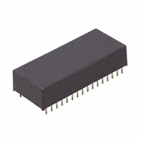
32-Pin DIP Module
PN484201.eps
Sept. 1996 C
1
A0–A16
Address input
CE
Chip enable
RST
Microprocessor reset
WE
Write enable
OE
Output enable
DQ0–DQ7
Data in/data out
INT
Programmable interrupt
VCC
+5 volts
VSS
Ground
�bq4842Y
modes, power-on reset timing, watchdog timer activation, and interrupt generation.
Functional Description
Figure 1 is a block diagram of the bq4842Y. The following sections describe the bq4842Y functional operation,
including memory and clock interface, data-retention
Figure 1. Block Diagram
Truth Table
VCC
CE
OE
WE
Mode
DQ
Power
< VCC (max.)
VIH
X
X
Deselect
High Z
Standby
VIL
X
VIL
Write
DIN
Active
VIL
VIL
VIH
Read
DOUT
Active
VIL
VIH
VIH
Read
High Z
Active
< VPFD (min.) > VSO
X
X
X
Deselect
High Z
CMOS standby
≤ VSO
X
X
X
Deselect
High Z
Battery-backup mode
> VCC (min.)
Sept. 1996 C
2
�bq4842Y
address inputs are changed while CE and OE remain low,
output data remains valid for tOH (output data hold time),
but goes indeterminate until the next address access.
Address Map
The bq4842Y provides 16 bytes of clock and control
status registers and 131,056 bytes of storage RAM.
Write Mode
Figure 2 illustrates the address map for the bq4842Y.
Table 1 is a map of the bq4842Y registers, and Table 2
describes the register bits.
The bq4842Y is in write mode whenever WE and CE are
active. The start of a write is referenced from the latteroccurring falling edge of WE or CE. A write is terminated
by the earlier rising edge of WE or CE. The addresses
must be held valid throughout the cycle. CE or WE must
return high for a minimum of tWR2 from CE or tWR1 from
WE prior to the initiation of another read or write cycle.
Memory Interface
Read Mode
The bq4842Y is in read mode whenever OE (output enable)
is low and CE (chip enable) is low. The device architecture
allows ripple-through access of data from eight of 1,048,576
locations in the static storage array. Thus, the unique address specified by the 17 address inputs defines which one
of the 131,072 bytes of data is to be accessed. Valid data is
available at the data I/O pins within tAA (address access
time) after the last address input signal is stable, providing
that the CE and OE (output enable) access times are also
satisfied. If the CE and OE access times are not met, valid
data is available after the latter of chip enable access time
(tACE) or output enable access time (tOE).
Data-in must be valid tDW prior to the end of write and remain valid for tDH1 or tDH2 afterward. OE should be kept
high during write cycles to avoid bus contention; although,
if the output bus has been activated by a low on CE and
OE, a low on WE disables the outputs tWZ after WE falls.
Data-Retention Mode
With valid VCC applied, the bq4842Y operates as a
conventional static RAM. Should the supply voltage
decay, the RAM automatically power-fail deselects,
write-protecting itself tWPT after VCC falls below VPFD.
All outputs become high impedance, and all inputs are
treated as “don’t care.”
CE and OE control the state of the eight three-state data
I/O signals. If the outputs are activated before tAA, the data
lines are driven to an indeterminate state until tAA. If the
16 Bytes
Clock and
Control Status
Registers
1FFFF
1FFF0
1FFEF
131,056
Bytes
1FFFF
1FFFE
1FFFD
1FFFC
1FFFB
1FFFA
1FFF9
1FFF8
1FFF7
1FFF6
1FFF5
1FFF4
1FFF3
1FFF2
14
Year
Month
Date
Days
Hours
Minutes
Seconds
Control
Watchdog
Interrupts
Alarm Date
Alarm Hours
Alarm Minutes
Alarm Seconds
Tenths/
Hundredths
15
Flags
1FFF0
0
1
2
3
4
5
6
7
8
9
10
11
12
13
Storage
RAM
0000
1FFF1
FG484201.eps
Figure 2. Address Map
Sept. 1996 C
3
�bq4842Y
should be halted. Updating is halted by setting the read
bit D6 of the control register to 1. As long as the read bit
is 1, updates to user-accessible clock locations are inhibited. Once the frozen clock information is retrieved by
reading the appropriate clock memory locations, the read
bit should be reset to 0 in order to allow updates to occur
from the internal counters. Because the internal counters are not halted by setting the read bit, reading the
clock locations has no effect on clock accuracy. Once the
read bit is reset to 0, within one second the internal registers update the user-accessible registers with the correct
time. A halt command issued during a clock update allows the update to occur before freezing the data.
If power-fail detection occurs during a valid access, the
memory cycle continues to completion. If the memory cycle
fails to terminate within time tWPT, write-protection takes
place. When VCC drops below VSO, the control circuit
switches power to the internal energy source, which preserves data.
The internal coin cell maintains data in the bq4842Y after
the initial application of VCC for an accumulated period of
at least 10 years when VCC is less than VSO. As system
power returns and Vcc rises above VSO, the battery is disconnected, and the power supply is switched to external
VCC. Write-protection continues for tCER after VCC reaches
VPFD to allow for processor stabilization. After tCER, normal RAM operation can resume.
Setting the Clock
Bit D7 of the control register is the write bit. Like the
read bit, the write bit when set to a 1 halts updates to
the clock/calendar memory locations. Once frozen, the
locations can be written with the desired information in
24-hour BCD format. Resetting the write bit to 0 causes
the written values to be transferred to the internal clock
counters and allows updates to the user-accessible registers to resume within one second. Use the write bit, D7,
only when updating the time registers (1FFF–1FFF9).
Clock Interface
Reading the Clock
The interface to the clock and control registers of the
bq4842Y is the same as that for the general-purpose storage memory. Once every second, the user-accessible
clock/calendar locations are updated simultaneously from
the internal real time counters. To prevent reading data
in transition, updates to the bq4842Y clock registers
Table 1. bq4842 Clock and Control Register Map
Address
D7
D6
1FFFF
D5
D4
D3
D2
10 Years
1FFFF
X
X
1FFFD
X
X
X
1FFFC
X
FTE
1FFFB
X
X
10 Month
X
D0
Register
Year
Month
01–12
Month
Date
01–31
Date
01–07
Days
Hours
00–23
Hours
Minutes
X
Day
10 Hours
Range (h)
00–99
10 Date
X
D1
Year
1FFFA
X
10 Minutes
Minutes
00–59
1FFF9
OSC
10 Seconds
Seconds
00–59
Seconds
1FFF8
W
00–31
Control
1FFF7
1FFF6
R
S
WDS
BM4
BM3
BM2
BM1
BM0
WD1
WD0
Watchdog
AIE
PWRIE
ABE
PIE
RS3
RS2
RS1
RS0
Interrupts
1FFF5
ALM3
X
10-date alarm
Alarm date
01–31
Alarm date
1FFF4
ALM2
X
10-hour alarm
Alarm hours
00–23
Alarm hours
1FFF3
ALM1
Alarm 10 minutes
Alarm minutes
00–59
Alarm minutes
1FFF2
ALM0
Alarm 10 seconds
Alarm seconds
00–59
Alarm seconds
0.01 seconds
00–99
0.1/0.01 seconds
1FFF1
1FFF0
Notes:
Calibration
0.1 seconds
WDF
AF
PWRF
BLF
PF
X
X
X
Flags
X = Unused bits; can be written and read.
Clock/Calendar data in 24-hour BCD format.
BLF = 1 for low battery.
OSC = 1 stops the clock oscillator.
Interrupt enables are cleared on power-up.
Sept. 1996 C
4
�bq4842Y
adjust the calibration based on the typical operating
temperature of individual applications.
Table 2. Clock and Control Register Bits
Bits
Description
ABE
Alarm interrupt enable in
battery-backup mode
AF
Alarm interrupt flag
AIE
Alarm interrupt enable
ALM0–ALM3
Alarm repeat rate
BLF
Battery-low flag
BM0–BM4
Watchdog multiplier
FTE
Frequency test mode enable
OSC
Oscillator stop
PF
Periodic interrupt flag
PIE
Periodic interrupt enable
PWRF
Power-fail interrupt flag
PWRIE
Power-fail interrupt enable
R
Read clock enable
RS0–RS3
Periodic interrupt rate
S
Calibration sign
W
Write clock enable
WD0–WD1
Watchdog resolution
WDF
Watchdog flag
WDS
Watchdog steering
The software calibration bits are located in the control register. Bits D0–D4 control the magnitude of correction, and
bit D5 the direction (positive or negative) of correction.
Assuming that the oscillator is running at exactly 32,786
Hz, each calibration step of D0–D4 adjusts the clock rate
by +4.068 ppm (+10.7 seconds per month) or -2.034 ppm
(-5.35 seconds per month) depending on the value of the
sign bit D5. When the sign bit is 1, positive adjustment
occurs; a 0 activates negative adjustment. The total range
of clock calibration is +5.5 or -2.75 minutes per month.
Two methods can be used to ascertain how much calibration a given bq4842Y may require in a system. The
first involves simply setting the clock, letting it run for a
month, and then comparing the time to an accurate
known reference like WWV radio broadcasts. Based on
the variation to the standard, the end user can adjust
the clock to match the system’s environment even after
the product is packaged in a non-serviceable enclosure.
The only requirement is a utility that allows the end
user to access the calibration bits in the control register.
The second approach uses a bq4842Y test mode. When the
frequency test mode enable bit FTE in the days register is
set to a 1, and the oscillator is running at exactly 32,768 Hz,
the LSB of the seconds register toggles at 512 Hz. Any deviation from 512 Hz indicates the degree and direction of oscillator frequency shift at the test temperature. For example,
a reading of 512.01024 Hz indicates a (1E6*0.01024)/512 or
+20 ppm oscillator frequency error, requiring ten steps of
negative calibration (10*-2.034 or -20.34) or 001010 to be
loaded into the calibration byte for correction. To read the
test frequency, the bq4842Y must be selected and held in an
extended read of the seconds register, location 1FFF9, with-
Stopping and Starting the Clock Oscillator
The OSC bit in the seconds register turns the clock on or
off. If the bq4842Y is to spend a significant period of
time in storage, the clock oscillator can be turned off to
preserve battery capacity. OSC set to 1 stops the clock
oscillator. When OSC is reset to 0, the clock oscillator is
turned on and clock updates to user-accessible memory
locations occur within one second.
The OSC bit is set to 1 when shipped from the Benchmarq factory.
Calibrating the Clock
The bq4842Y real-time clock is driven by a quartz controlled oscillator with a nominal frequency of 32,768 Hz.
The quartz crystal is contained within the bq4842Y
package along with the battery. The clock accuracy of
the bq4842Y module is tested to be within 20ppm or
about 1 minute per month at 25°C. The oscillation rates
of crystals change with temperature as Figure 3 shows.
To compensate for the frequency shift, the bq4842Y offers onboard software clock calibration. The user can
Figure 3. Frequency Error
Sept. 1996 C
5
�bq4842Y
out having the read bit set. The frequency appears on
DQ0. The FTE bit must be set using the write bit control. The FTE bit must be reset to 0 for normal clock operation to resume.
Interrupts
The bq4842Y allows four individually selected interrupt
events to generate an interrupt request on the INT pin.
These four interrupt events are:
Power-On Reset
■
The bq4842Y provides a power-on reset, which pulls the
RST pin low on power-down and remains low on powerup for tCER after VCC passes VPFD.
The watchdog timer interrupt, programmable to
occur according to the time-out period and conditions
described in the watchdog timer section.
■
The periodic interrupt, programmable to occur once
every 122µs to 500ms.
■
The alarm interrupt, programmable to occur once per
second to once per month.
■
The power-fail interrupt, which can be enabled to be
asserted when the bq4842Y detects a power failure.
Watchdog Timer
The watchdog circuit monitors the microprocessor’s activity. If the processor does not reset the watchdog timer
within the programmed time-out period, the circuit asserts the INT or RST pin. The watchdog timer is activated by writing the desired time-out period into the
eight-bit watchdog register described in Table 3 (device
address 1FFF7). The five bits (BM4–BM0) store a binary m ult iplie r, and t he t w o lo w e r- o rd e r b i ts
(WD1–WD0) select the resolution, where 00 = 1 16 second,
01 = 1 4 second, 10 = 1 second, and 11 = 4 seconds.
The periodic, alarm, and power-fail interrupts are enabled by an individual interrupt-enable bit in register
1FFF6, the interrupts register. When an event occurs,
its event flag bit in the flags register, location 1FFF0, is
set. If the corresponding event enable bit is also set,
then an interrupt request is generated. Reading the
flags register clears all flag bits and makes INT high impedance. To reset the flag register, the bq4842Y addresses must be held stable at location 1FFF0 for at
least 50ns to avoid inadvertent resets.
The time-out period is the multiplication of the five-bit multiplier with the two-bit resolution. For example, writing 00011
in BM4–BM0 and 10 in WD1–WD0 results in a total timeout setting of 3 x 1 or 3 seconds. A multiplier of zero disables
the watchdog circuit. Bit 7 of the watchdog register (WDS) is
the watchdog steering bit. When WDS is set to a 1 and a
time-out occurs, the watchdog asserts a reset pulse for tCER
on the RST pin. During the reset pulse, the watchdog register is cleared to all zeros disabling the watchdog. When
WDS is set to a 0, the watchdog asserts the INT pin on a
time-out. The INT pin remains low until the watchdog is reset by the microprocessor or a power failure occurs. Additionally, when the watchdog times out, the watchdog flag bit
(WDF) in the flags register, location 1FFF0, is set.
Periodic Interrupt
Bits RS3–RS0 in the interrupts register program the rate
for the periodic interrupt. The user can interpret the interrupt in two ways: either by polling the flags register for PF
assertion or by setting PIE so that INT goes active when
the bq4842Y sets the periodic flag. Reading the flags register resets the PF bit and returns INT to the highimpedance state. Table 4 shows the periodic rates.
Alarm Interrupt
To reset the watchdog timer, the microprocessor must write
to the watchdog register. After being reset by a write, the
watchdog time-out period starts over. As a precaution, the
watchdog circuit is disabled on a power failure. The user
must, therefore, set the watchdog at boot-up for activation.
Registers 1FFF5–1FFF2 program the real-time clock
alarm. During each update cycle, the bq4842Y compares the date, hours, minutes, and seconds in the clock
registers with the corresponding alarm registers. If a
match between all the corresponding bytes is found, the
alarm flag AF in the flags register is set. If the alarm
interrupt is enabled with AIE, an interrupt request is
generated on INT. The alarm condition is cleared by a
read to the flags register. ALM3–ALM0 puts the alarm
Table 3. Watchdog Register Bits
MSB
Bits
LSB
7
6
5
4
3
2
1
0
WDS
BM4
BM3
BM2
BM1
BM0
WD1
WD0
Sept. 1996 C
6
�bq4842Y
into a periodic mode of operation. Table 5 describes the
selectable rates.
Power-Fail Interrupt
When VCC falls to the power-fail-detect point, the power-fail
flag PWRF is set. If the power-fail interrupt enable bit
(PWRIE) is also set, then INT is asserted low. The powerfail interrupt occurs tWPT before the bq4842Y generates a
reset and deselects. The PWIE bit is cleared on power-up.
The alarm interrupt can be made active while the bq4842Y
is in the battery-backup mode by setting ABE in the interrupts register. Normally, the INT pin tri-states during battery backup. With ABE set, however, INT is driven low if
an alarm condition occurs and the AIE bit is set. Because
the AIE bit is reset during power-on reset, an alarm generated during power-on reset updates only the flags register.
The user can read the flags register during boot-up to determine if an alarm was generated during power-on reset.
Battery-Low Warning
The bq4842Y checks the internal battery on power-up.
If the battery voltage is below 2.2V, the battery-low flag
BLF in the flags register is set to a 1 indicating that
clock and RAM data may be invalid.
Table 4. Periodic Rates
RS3
RS2
RS1
RS0
0
0
0
0
Interrupt Rate
None
0
0
0
1
10ms
0
0
1
0
100ms
0
0
1
1
122.07µs
0
1
0
0
244.14µs
0
1
0
1
488.281
0
1
1
0
976.5625
0
1
1
1
1.953125ms
1
0
0
0
3.90625ms
1
0
0
1
7.8125ms
1
0
1
0
15.625ms
1
0
1
1
31.25ms
1
1
0
0
62.5ms
1
1
0
1
125ms
1
1
1
0
250ms
1
1
1
1
500ms
Table 5. Alarm Frequency (Alarm Bits DQ7 of Alarm Registers)
ALM3
ALM2
ALM1
ALM0
1
1
1
1
Alarm Frequency
1
1
1
0
Once per minute when seconds match
1
1
0
0
Once per hour when minutes, and seconds match
1
0
0
0
Once per day when hours, minutes, and seconds match
0
0
0
0
When date, hours, minutes, and seconds match
Once per second
Sept. 1996 C
7
�bq4842Y
Absolute Maximum Ratings
Symbol
Parameter
Value
Unit
VCC
DC voltage applied on VCC relative to VSS
-0.3 to 7.0
V
VT
DC voltage applied on any pin excluding VCC
relative to VSS
-0.3 to 7.0
V
TOPR
Operating temperature
0 to +70
°C
TSTG
Storage temperature (VCC off; oscillator off)
-40 to +70
°C
TBIAS
Temperature under bias
-10 to +70
°C
TSOLDER
Soldering temperature
+260
°C
Note:
Conditions
VT ≤ VCC + 0.3
For 10 seconds
Permanent device damage may occur if Absolute Maximum Ratings are exceeded. Functional operation
should be limited to the Recommended DC Operating Conditions detailed in this data sheet. Exposure to
conditions beyond the operational limits for extended periods of time may affect device reliability.
Recommended DC Operating Conditions (TA = TOPR)
Symbol
Note:
Parameter
Minimum
Typical
Maximum
Unit
VCC
Supply voltage
4.5
5.0
5.5
V
VSS
Supply voltage
0
0
0
V
VIL
Input low voltage
-0.3
-
0.8
V
VIH
Input high voltage
2.2
-
VCC + 0.3
V
Notes
Typical values indicate operation at TA = 25°C.
Sept. 1996 C
8
�bq4842Y
DC Electrical Characteristics (TA = TOPR, VCCmin ≤ VCC ≤ VCCmax)
Minimum
Typical
Maximum
Unit
ILI
Symbol
Input leakage current
Parameter
-
-
±1
µA
VIN = VSS to VCC
Conditions/Notes
ILO
Output leakage current
-
-
±1
µA
CE = VIH or OE = VIH or
WE = VIL
VOH
Output high voltage
2.4
-
-
V
IOH = -1.0 mA
VOL
Output low voltage
-
-
0.4
V
IOL = 2.1 mA
IOD
RST, INT sink current
10
-
-
mA
VOL = 0.4V
ISB1
Standby supply current
-
3
6
mA
CE = VIH
ISB2
Standby supply current
-
2
4
mA
CE ≥ VCC - 0.2V,
0V ≤ VIN ≤ 0.2V,
or VIN ≥ VCC - 0.2V
ICC
Operating supply current
-
75
105
mA
Min. cycle, duty = 100%,
CE = VIL, II/O = 0mA
VPFD
Power-fail-detect voltage
4.30
4.37
4.50
V
VSO
Supply switch-over voltage
-
3
-
V
Notes:
Typical values indicate operation at TA = 25°C, VCC = 5V.
RST and INT are open-drain outputs.
Capacitance (TA = 25°C, F = 1MHz, VCC = 5.0V)
Symbol
Parameter
Minimum
Typical
Maximum
Unit
CI/O
Input/output capacitance
-
-
10
pF
Output voltage = 0V
CIN
Input capacitance
-
-
10
pF
Input voltage = 0V
Note:
These parameters are sampled and not 100% tested.
Sept. 1996 C
9
Conditions
�bq4842Y
AC Test Conditions
Parameter
Test Conditions
Input pulse levels
0V to 3.0V
Input rise and fall times
5 ns
Input and output timing reference levels
1.5 V (unless otherwise specified)
Output load (including scope and jig)
See Figures 4 and 5
Figure 4. Output Load A
Read Cycle
Figure 5. Output Load B
(TA = TOPR, VCCmin ≤ VCC ≤ VCCmax)
-85
Symbol
Parameter
Min.
Max.
Unit
85
-
ns
Conditions
tRC
Read cycle time
tAA
Address access time
-
85
ns
Output load A
tACE
Chip enable access time
-
85
ns
Output load A
tOE
Output enable to output valid
-
45
ns
Output load A
tCLZ
Chip enable to output in low Z
5
-
ns
Output load B
tOLZ
Output enable to output in low Z
0
-
ns
Output load B
tCHZ
Chip disable to output in high Z
0
35
ns
Output load B
tOHZ
Output disable to output in high Z
0
25
ns
Output load B
tOH
Output hold from address change
10
-
ns
Output load A
Sept. 1996 C
10
�bq4842Y
Read Cycle No. 1 (Address Access) 1,2
Read Cycle No. 2 (CE Access) 1,3,4
Read Cycle No. 3 (OE Access) 1,5
Notes:
1. WE is held high for a read cycle.
2. Device is continuously selected: CE = OE = VIL.
3. Address is valid prior to or coincident with CE transition low.
4. OE = VIL.
5. Device is continuously selected: CE = VIL.
Sept. 1996 C
11
�bq4842Y
Write Cycle
(TA =TOPR , VCCmin ≤ VCC ≤ VCCmax)
-85
Symbol
Parameter
Min.
Max.
Units
Conditions/Notes
tWC
Write cycle time
85
-
ns
tCW
Chip enable to end of write
75
-
ns
(1)
tAW
Address valid to end of write
75
-
ns
(1)
tAS
Address setup time
0
-
ns
Measured from address valid to beginning of write. (2)
tWP
Write pulse width
65
-
ns
Measured from beginning of write to
end of write. (1)
tWR1
Write recovery time (write cycle 1)
5
-
ns
Measured from WE going high to end
of write cycle. (3)
tWR2
Write recovery time (write cycle 2)
15
-
ns
Measured from CE going high to end of
write cycle. (3)
tDW
Data valid to end of write
35
-
ns
Measured to first low-to-high transition of either CE or WE.
tDH1
Data hold time (write cycle 1)
0
-
ns
Measured from WE going high to end
of write cycle. (4)
tDH2
Data hold time (write cycle 2)
10
-
ns
Measured from CE going high to end of
write cycle. (4)
tWZ
Write enabled to output in high Z
0
30
ns
I/O pins are in output state. (5)
tOW
Output active from end of write
0
-
ns
I/O pins are in output state. (5)
Notes:
1. A write ends at the earlier transition of CE going high and WE going high.
2. A write occurs during the overlap of a low CE and a low WE. A write begins at the later transition
of CE going low and WE going low.
3. Either tWR1 or tWR2 must be met.
4. Either tDH1 or tDH2 must be met.
5. If CE goes low simultaneously with WE going low or after WE going low, the outputs remain in
high-impedance state.
Sept. 1996 C
12
�bq4842Y
Write Cycle No. 1 (WE-Controlled) 1,2,3
Write Cycle No. 2 (CE-Controlled) 1,2,3,4,5
Notes:
1. CE or WE must be high during address transition.
2. Because I/O may be active (OE low) during this period, data input signals of opposite polarity to the
outputs must not be applied.
3. If OE is high, the I/O pins remain in a state of high impedance.
4. Either tWR1 or tWR2 must be met.
5. Either tDH1 or tDH2 must be met.
Sept. 1996 C
13
�bq4842Y
Power-Down/Power-Up Cycle (TA = TOPR)
Symbol
Minimum
Typical
Maximum
Unit
tPF
VCC slew, 4.50 to 4.20 V
300
-
-
µs
tFS
VCC slew, 4.20 to VSO
10
-
-
µs
tPU
VCC slew, VSO to VPFD
(max.)
0
-
-
µs
tCER
Chip enable recovery time
40
100
200
ms
tDR
Data-retention time in
absence of VCC
10
-
-
years
tWPT
Write-protect time
40
100
160
µs
Notes:
Parameter
Conditions
Time during which SRAM is
write-protected after VCC
passes VFPD on power-up.
TA = 25°C. (2)
Delay after VCC slews down
past VPFD before SRAM is
write-protected.
1. Typical values indicate operation at TA = 25°C, VCC = 5V.
2. Battery is disconnected from circuit until after VCC is applied for the first time. tDR is the
accumulated time in absence of power beginning when power is first applied to the device.
Caution: Negative undershoots below the absolute maximum rating of -0.3V in battery-backup mode
may affect data integrity.
Power-Down/Power-Up Timing
Notes:
1. PWRIE is set to “1” to enable power fail interrupt.
2. RST and INT are open drain and require an external pull-up resistor.
Sept. 1996 C
14
�bq4842Y
Data Sheet Revision History
Change No.
Page No.
1
4
Corrected the locations of bits D6 and D4 of the Interrupts Register and the corresponding bits D5 and D3 of the Flags Register (these were reversed).
2
4
Corrected the alarm date register (7FF5) to allow for 01-31 days in a month instead
of 01-07 days.
2
9
Lowered ISB1 from 4 typ. and 7 max. to 3, 6.
Lowered ISB2 typ. from 2.5 to 2.
Notes:
Description
Change 1 = Mar. 1996 B changes from Oct. 1995 A.
Change 2 = Sept. 1996 C changes from Mar. 1996 B.
Sept. 1996 C
15
�bq4842Y
MA: 32-Pin A-Type Module
32-Pin MA (A-Type Module)
Inches
Millimeters
Dimension
Min.
Max.
Min.
Max.
A
0.365
0.375
9.27
9.53
A1
0.015
-
0.38
-
B
0.017
0.023
0.43
0.58
C
0.008
0.013
0.20
0.33
D
1.670
1.700
42.42
43.18
E
0.710
0.740
18.03
18.80
e
0.590
0.630
14.99
16.00
G
0.090
0.110
2.29
2.79
L
0.120
0.150
3.05
3.81
S
0.075
0.110
1.91
2.79
Sept. 1996 C
16
�bq4842Y
Ordering Information
bq4842Y MA Speed Options:
85 = 85 ns
Package Option:
MA = A-type module
Device:
bq4842Y 128K x 8 Real-Time Clock Module
Sept. 1996 C
17
�IMPORTANT NOTICE
Texas Instruments and its subsidiaries (TI) reserve the right to make changes to their products or to discontinue
any product or service without notice, and advise customers to obtain the latest version of relevant information
to verify, before placing orders, that information being relied on is current and complete. All products are sold
subject to the terms and conditions of sale supplied at the time of order acknowledgement, including those
pertaining to warranty, patent infringement, and limitation of liability.
TI warrants performance of its semiconductor products to the specifications applicable at the time of sale in
accordance with TI’s standard warranty. Testing and other quality control techniques are utilized to the extent
TI deems necessary to support this warranty. Specific testing of all parameters of each device is not necessarily
performed, except those mandated by government requirements.
CERTAIN APPLICATIONS USING SEMICONDUCTOR PRODUCTS MAY INVOLVE POTENTIAL RISKS OF
DEATH, PERSONAL INJURY, OR SEVERE PROPERTY OR ENVIRONMENTAL DAMAGE (“CRITICAL
APPLICATIONS”). TI SEMICONDUCTOR PRODUCTS ARE NOT DESIGNED, AUTHORIZED, OR
WARRANTED TO BE SUITABLE FOR USE IN LIFE-SUPPORT DEVICES OR SYSTEMS OR OTHER
CRITICAL APPLICATIONS. INCLUSION OF TI PRODUCTS IN SUCH APPLICATIONS IS UNDERSTOOD TO
BE FULLY AT THE CUSTOMER’S RISK.
In order to minimize risks associated with the customer’s applications, adequate design and operating
safeguards must be provided by the customer to minimize inherent or procedural hazards.
TI assumes no liability for applications assistance or customer product design. TI does not warrant or represent
that any license, either express or implied, is granted under any patent right, copyright, mask work right, or other
intellectual property right of TI covering or relating to any combination, machine, or process in which such
semiconductor products or services might be or are used. TI’s publication of information regarding any third
party’s products or services does not constitute TI’s approval, warranty or endorsement thereof.
Copyright 1999, Texas Instruments Incorporated
�