Not Recommended For New Designs
bq4847/bq4847Y
RTC Module With CPU Supervisor
Features
General Description
tolerance to allow for power supply
and processor stabilization.
➤ Real-Time Clock counts seconds
through years in BCD format
The bq4847 Real-Time Clock Module is a low-power microprocessor
peripheral that integrates a timeof-day clock, a 100-year calendar, a
CPU supervisor, a battery, and a crystal in a 28-pin DIP module. The part
is ideal for fax machines, copiers, industrial control systems, point-of-sale
terminals, data loggers, and computers.
The bq4847 also has a built-in
watchdog timer to monitor processor
operation. If the microprocessor does
not toggle the watchdog input (WDI)
within the programmed time-out,
the bq4847 asserts WDO and RST.
WDI unconnected disables the
watchdog timer.
➤ Integrated battery and crystal
➤ On-chip battery-backup switchover circuit with nonvolatile control for an external SRAM
➤ 130mAh battery capacity
➤ ± 1 minute per month clock accuracy
➤ Less than 500nA of clock operation current in backup mode
➤ Microprocessor reset valid to
VCC = VSS
➤ Independent watchdog timer
with a programmable time-out
period
➤ Power-fail interrupt warning
➤ Programmable clock alarm interrupt active in battery-backup
mode
➤ Programmable periodic interrupt
➤ Battery-low warning
Pin Connections
VOUT
NC
NC
WDO
INT
RST
A3
A2
A1
A0
DQ0
DQ1
DQ2
VSS
1
2
3
4
5
6
7
8
9
10
11
12
13
14
28
27
26
25
24
23
22
21
20
19
18
17
16
15
The bq4847 contains an internal
battery and crystal. Through the use
of the conditional chip enable output
(CEOUT) and battery voltage output
(VOUT) pins, the bq4847 can writeprotect and make nonvolatile an
external SRAM. The backup cell
powers the real-time clock and
maintains SRAM information in
the absence of system voltage.
The
bq4847
contains
a
temperature-compensated reference and comparator circuit that
monitors the status of its voltage
supply. When an out-of-tolerance
condition is detected, the bq4847
generates an interrupt warning
and subsequently a microprocessor reset. The reset stays active
for 200ms after V CC rises within
The bq4847 can generate other interrupts based on a clock alarm condition or a periodic setting. The
alarm interrupt can be set to occur
from once per second to once per
month. The alarm can be made active in the battery-backup mode to
serve as a system wake-up call. For
interrupts at a rate beyond once per
second, the periodic interrupt can be
programmed with periods of 30.5µs
to 500ms.
Caution:
Take care to avoid inadvertent discharge through VOUT and CEOUT
after battery isolation has been
broken.
Pin Names
VCC
WE
CEIN
CEOUT
NC
WDI
OE
CS
NC
DQ7
DQ6
DQ5
DQ4
DQ3
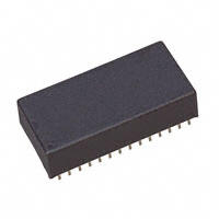
28-Pin DIP Module
PN484701.eps
A0–A3
Clock/Control address
inputs
DQ0–DQ7
Data inputs/outputs
WE
Write enable
OE
Output enable
CS
Chip select input
CEIN
External RAM chip
enable
CEOUT
Conditional RAM chip
enable
Sept. 1996
1
NC
No connect
VOUT
Back-up battery output
INT
Interrupt output
RST
Microprocessor reset
WDI
Watchdog input
WDO
Watchdog output
VCC
+5V supply
VSS
Ground
�Not Recommended For New Designs
bq4847/bq4847Y
room temperature. For a complete description of features, operating conditions, electrical characteristics,
bus timing, and pin descriptions, see the bq4845 data
sheet. Valid part types for ordering are bq4847MT (5%)
and bq4847YMT (10%).
Functional Description
Figure 1 is a block diagram of the bq4847. The bq4847 is
functionally equivalent to the bq4845 except that the battery (20, 24) and crystal (2, 3) pins are not accessible. The
pins are connected internally to a coin cell and quartz
crystal. The coin cell provides 130mAh of capacity. It is internally isolated from VOUT and CEOUT until the initial
application of VCC. Once VCC rises above VPFD, this isolation is broken, and the backup cell provides power to
VOUT and CEOUT for the external SRAM. The real-time
clock keeps time to within one minute per month at
Figure 2 illustrates the address map for the bq4847. Table 1 is a map of the bq4847 registers, and Table 2 describes the register bits.
Figure 1. Block Diagram
Truth Table
VCC
CS
OE
WE
CEOUT
VOUT
Mode
DQ
Power
< VCC (max.)
VIH
X
X
CEIN
VOUT1
Deselect
High Z
Standby
VIL
X
VIL
CEIN
VOUT1
Write
DIN
Active
> VCC (min.)
VIL
VIL
VIH
CEIN
VOUT1
Read
DOUT
Active
VIL
VIH
VIH
CEIN
VOUT1
Read
High Z
Active
< VPFD (min.) > VSO
X
X
X
VOH
VOUT1
Deselect
High Z
CMOS standby
≤ VSO
X
X
X
VOHB
VOUT2
Deselect
High Z
Battery-backup mode
Sept. 1996
2
�Not Recommended For New Designs
bq4847/bq4847Y
MT: 28-Pin T-Type Module
28-Pin MT (T-Type Module)
Inches
Millimeters
Dimension
Min.
Max.
Min.
Max.
A
0.360
0.390
9.14
9.91
A1
0.015
-
0.38
-
B
0.015
0.022
0.38
0.56
C
0.008
0.013
0.20
0.33
D
1.520
1.535
38.61
38.99
E
0.710
0.740
18.03
18.80
e
0.590
0.620
14.99
15.75
G
0.090
0.110
2.29
2.79
L
0.110
0.130
2.79
3.30
S
0.100
0.120
2.54
3.05
Ordering Information
bq4847
- MT
Package Option:
MT = 28-pin T-type Module
Voltage Tolerance:
Blank = 5%
Y = 10%
Device:
bq4847 Real-Time Clock Module With CPU Supervisor
Sept. 1996
3
�PACKAGE OPTION ADDENDUM
www.ti.com
31-Mar-2014
PACKAGING INFORMATION
Orderable Device
Status
(1)
Package Type Package Pins Package
Drawing
Qty
Eco Plan
Lead/Ball Finish
MSL Peak Temp
(2)
(6)
(3)
Op Temp (°C)
Device Marking
(4/5)
BQ4847MT
OBSOLETE DIP MODULE
MT
28
TBD
Call TI
Call TI
0 to 70
BQ4847YMT
OBSOLETE DIP MODULE
MT
28
TBD
Call TI
Call TI
0 to 70
(1)
The marketing status values are defined as follows:
ACTIVE: Product device recommended for new designs.
LIFEBUY: TI has announced that the device will be discontinued, and a lifetime-buy period is in effect.
NRND: Not recommended for new designs. Device is in production to support existing customers, but TI does not recommend using this part in a new design.
PREVIEW: Device has been announced but is not in production. Samples may or may not be available.
OBSOLETE: TI has discontinued the production of the device.
(2)
Eco Plan - The planned eco-friendly classification: Pb-Free (RoHS), Pb-Free (RoHS Exempt), or Green (RoHS & no Sb/Br) - please check http://www.ti.com/productcontent for the latest availability
information and additional product content details.
TBD: The Pb-Free/Green conversion plan has not been defined.
Pb-Free (RoHS): TI's terms "Lead-Free" or "Pb-Free" mean semiconductor products that are compatible with the current RoHS requirements for all 6 substances, including the requirement that
lead not exceed 0.1% by weight in homogeneous materials. Where designed to be soldered at high temperatures, TI Pb-Free products are suitable for use in specified lead-free processes.
Pb-Free (RoHS Exempt): This component has a RoHS exemption for either 1) lead-based flip-chip solder bumps used between the die and package, or 2) lead-based die adhesive used between
the die and leadframe. The component is otherwise considered Pb-Free (RoHS compatible) as defined above.
Green (RoHS & no Sb/Br): TI defines "Green" to mean Pb-Free (RoHS compatible), and free of Bromine (Br) and Antimony (Sb) based flame retardants (Br or Sb do not exceed 0.1% by weight
in homogeneous material)
(3)
MSL, Peak Temp. - The Moisture Sensitivity Level rating according to the JEDEC industry standard classifications, and peak solder temperature.
(4)
There may be additional marking, which relates to the logo, the lot trace code information, or the environmental category on the device.
(5)
Multiple Device Markings will be inside parentheses. Only one Device Marking contained in parentheses and separated by a "~" will appear on a device. If a line is indented then it is a continuation
of the previous line and the two combined represent the entire Device Marking for that device.
(6)
Lead/Ball Finish - Orderable Devices may have multiple material finish options. Finish options are separated by a vertical ruled line. Lead/Ball Finish values may wrap to two lines if the finish
value exceeds the maximum column width.
Important Information and Disclaimer:The information provided on this page represents TI's knowledge and belief as of the date that it is provided. TI bases its knowledge and belief on information
provided by third parties, and makes no representation or warranty as to the accuracy of such information. Efforts are underway to better integrate information from third parties. TI has taken and
continues to take reasonable steps to provide representative and accurate information but may not have conducted destructive testing or chemical analysis on incoming materials and chemicals.
TI and TI suppliers consider certain information to be proprietary, and thus CAS numbers and other limited information may not be available for release.
In no event shall TI's liability arising out of such information exceed the total purchase price of the TI part(s) at issue in this document sold by TI to Customer on an annual basis.
Addendum-Page 1
Samples
�PACKAGE OPTION ADDENDUM
www.ti.com
31-Mar-2014
Addendum-Page 2
�MECHANICAL DATA
MPDI064 – MAY 2001
MT (R-PDIP-T**)
PLASTIC DUAL-IN-LINE
28 PINS SHOWN
Inches
D
Millimeters
Min.
Dimension
Min.
Max.
A
0.360
0.390
9.14
A1
0.015
0.38
Max.
9.91
–
B
0.015
–
0.022
0.38
0.56
C
0.008
0.013
0.20
0.33
D/24 PIN
1.320
1.335
33.53
33.91
D/28 PIN
1.520
1.535
38.61
38.99
E
0.710
0.740
18.03
18.80
e
G
0.590
0.630
16.00
0.090
0.110
14.99
2.29
L
0.110
2.79
3.30
S
0.100
0.130
0.120
2.54
3.05
2.79
E
A1
A
C
B
L
S
e
G
4201978/A 03/01
NOTES: A. All linear dimensions are in inches (mm).
B. This drawing is subject to change without notice.
•
POST OFFICE BOX 655303 DALLAS, TEXAS 75265
POST OFFICE BOX 1443 HOUSTON, TEXAS 77251–1443
•
1
�IMPORTANT NOTICE
Texas Instruments Incorporated and its subsidiaries (TI) reserve the right to make corrections, enhancements, improvements and other
changes to its semiconductor products and services per JESD46, latest issue, and to discontinue any product or service per JESD48, latest
issue. Buyers should obtain the latest relevant information before placing orders and should verify that such information is current and
complete. All semiconductor products (also referred to herein as “components”) are sold subject to TI’s terms and conditions of sale
supplied at the time of order acknowledgment.
TI warrants performance of its components to the specifications applicable at the time of sale, in accordance with the warranty in TI’s terms
and conditions of sale of semiconductor products. Testing and other quality control techniques are used to the extent TI deems necessary
to support this warranty. Except where mandated by applicable law, testing of all parameters of each component is not necessarily
performed.
TI assumes no liability for applications assistance or the design of Buyers’ products. Buyers are responsible for their products and
applications using TI components. To minimize the risks associated with Buyers’ products and applications, Buyers should provide
adequate design and operating safeguards.
TI does not warrant or represent that any license, either express or implied, is granted under any patent right, copyright, mask work right, or
other intellectual property right relating to any combination, machine, or process in which TI components or services are used. Information
published by TI regarding third-party products or services does not constitute a license to use such products or services or a warranty or
endorsement thereof. Use of such information may require a license from a third party under the patents or other intellectual property of the
third party, or a license from TI under the patents or other intellectual property of TI.
Reproduction of significant portions of TI information in TI data books or data sheets is permissible only if reproduction is without alteration
and is accompanied by all associated warranties, conditions, limitations, and notices. TI is not responsible or liable for such altered
documentation. Information of third parties may be subject to additional restrictions.
Resale of TI components or services with statements different from or beyond the parameters stated by TI for that component or service
voids all express and any implied warranties for the associated TI component or service and is an unfair and deceptive business practice.
TI is not responsible or liable for any such statements.
Buyer acknowledges and agrees that it is solely responsible for compliance with all legal, regulatory and safety-related requirements
concerning its products, and any use of TI components in its applications, notwithstanding any applications-related information or support
that may be provided by TI. Buyer represents and agrees that it has all the necessary expertise to create and implement safeguards which
anticipate dangerous consequences of failures, monitor failures and their consequences, lessen the likelihood of failures that might cause
harm and take appropriate remedial actions. Buyer will fully indemnify TI and its representatives against any damages arising out of the use
of any TI components in safety-critical applications.
In some cases, TI components may be promoted specifically to facilitate safety-related applications. With such components, TI’s goal is to
help enable customers to design and create their own end-product solutions that meet applicable functional safety standards and
requirements. Nonetheless, such components are subject to these terms.
No TI components are authorized for use in FDA Class III (or similar life-critical medical equipment) unless authorized officers of the parties
have executed a special agreement specifically governing such use.
Only those TI components which TI has specifically designated as military grade or “enhanced plastic” are designed and intended for use in
military/aerospace applications or environments. Buyer acknowledges and agrees that any military or aerospace use of TI components
which have not been so designated is solely at the Buyer's risk, and that Buyer is solely responsible for compliance with all legal and
regulatory requirements in connection with such use.
TI has specifically designated certain components as meeting ISO/TS16949 requirements, mainly for automotive use. In any case of use of
non-designated products, TI will not be responsible for any failure to meet ISO/TS16949.
Products
Applications
Audio
www.ti.com/audio
Automotive and Transportation
www.ti.com/automotive
Amplifiers
amplifier.ti.com
Communications and Telecom
www.ti.com/communications
Data Converters
dataconverter.ti.com
Computers and Peripherals
www.ti.com/computers
DLP® Products
www.dlp.com
Consumer Electronics
www.ti.com/consumer-apps
DSP
dsp.ti.com
Energy and Lighting
www.ti.com/energy
Clocks and Timers
www.ti.com/clocks
Industrial
www.ti.com/industrial
Interface
interface.ti.com
Medical
www.ti.com/medical
Logic
logic.ti.com
Security
www.ti.com/security
Power Mgmt
power.ti.com
Space, Avionics and Defense
www.ti.com/space-avionics-defense
Microcontrollers
microcontroller.ti.com
Video and Imaging
www.ti.com/video
RFID
www.ti-rfid.com
OMAP Applications Processors
www.ti.com/omap
TI E2E Community
e2e.ti.com
Wireless Connectivity
www.ti.com/wirelessconnectivity
Mailing Address: Texas Instruments, Post Office Box 655303, Dallas, Texas 75265
Copyright © 2014, Texas Instruments Incorporated
�


 工商网监
湘ICP备2023018690号
工商网监
湘ICP备2023018690号
