Sample &
Buy
Product
Folder
Support &
Community
Tools &
Software
Technical
Documents
bq76PL455A-Q1
SLUSC51C – APRIL 2015 – REVISED NOVEMBER 2016
bq76PL455A-Q1 16-Cell EV/HEV Integrated Battery Monitor and Protector
1 Features
2 Applications
•
•
•
1
•
•
•
•
•
Monitors and Balances 6-to-16 Cells per Device
Highly Accurate Monitoring
– High Performance 14-bit Analog-to-Digital
Converter (ADC) With Internal Reference
– All Cells Converted in 2.4 ms (Nominal)
– Eight AUX Inputs for Temperature and Other
Sensors with Input Voltage of 0 V to 5 V
– Internal Precision Reference
Integrated Protector With Separate Vref for
Overvoltage (OV) and Undervoltage (UV)
Comparators and Programmable VCELL Set Points
Engineered for High System Robustness
– Up to 1-Mb/s Stackable Isolated DifferentialUART
– Up to 16 ICs in Daisy-Chain With Twisted Pair
– Passes Bulk Current Injection (BCI) Test
– Designed for Robust Hot-Plug Performance
Passive Balancing with External n-FETs and
Active Balancing with EMB1428Q/EMB1499Q
Can Help Customers Meet Functional Safety
Standard Requirements (For Example, ISO26262)
– Built-in Self-Tests to Validate Defined Internal
Functions
– Support for Open Wire Detection
AEC-Q100 Qualified With the Following Results:
– Device Temperature Grade 2: –40°C to 105°C
Ambient Operating Temperature Range
– Device HBM ESD Classification Level 2
– Device CDM ESD Classification Level C3
Electric and Hybrid Electric Vehicles (EV, HEV,
PHEV, Mild Hybrid)
48-V Systems (Single-Chip Solution)
Energy Storage (ESS) and UPS
E-Bikes, E-Scooters
•
•
•
3 Description
The bq76PL455A-Q1 device is an integrated 16-cell
battery monitoring and protection device, designed for
high-reliability automotive applications. The integrated
high-speed,
differential,
capacitor-isolated
communications interface allows up to sixteen
bq76PL455A-Q1 devices to communicate with a host
via a single high-speed Universal Asynchronous
Receiver/Transmitter (UART) interface.
The bq76PL455A-Q1 monitors and detects several
different fault conditions, including: overvoltage,
undervoltage, overtemperature, and communication
faults. Six GPIO ports as well as eight analog AUX
ADC inputs are included for additional monitoring and
programmable functionality. A secondary thermal
shutdown is included for further protection.
The bq76PL455A-Q1 has features that customers
may find useful to help them meet functional safety
standard requirements. See Safety Manual for
bq76PL455A-Q1 (SLUUB67).
Device Information(1)
PART NUMBER
PACKAGE
bq76PL455A-Q1
TQFP (80)
BODY SIZE (NOM)
12.00 mm × 12.00 mm
(1) For all available packages, see the orderable addendum at
the end of the data sheet.
Simplified Schematic
²
+
All GND connections
are local to this IC. See
text for layout details.
High
Current
Bus
Cell Balancing Circuits
Low Pass Filters Protection
16
16
Cell Balancing Circuits
Low Pass Filters Protection
All GND connections
are local to this IC. See
text for layout details.
VSENSE16
VSENSE1
VSENSE0
EQx
GND
CHP
COMML±
VM
COMML+
COMMH±
CHM
COMMH+
COMML±
OUT2
OUT1
V5VAO
VREF
VSENSE16
VSENSE1
VSENSE0
EQx
CHP
CHM
VM
OUT2
OUT1
V5VAO
VREF
COMML+
COMMH+
COMMH±
To Additional
Battery Monitors
GND
FAULTL±
FAULTH±
FAULTL+
FAULTH+
FAULTH±
FAULTL+
FAULTH+
TOP
VP
NPNB
VDIG
AUX7
GPIO (Out)
GPIO (In)
TX
RX
Texas Instruments
µC
C2000Œ
TMS570Œ
RT
RT
Cell Temperature
Measurement
AUX0
VIO
GPIO0..5
WAKEUP
FAULT_N
TX
RX
TOP
VP
NPNB
VDIG
AUX7
AUX0
VIO
GPIO0..5
WAKEUP
FAULT_N
TX
RX
Differential
Signaling
Daisy-Chain
FAULTL±
VP
I/O Power
Supply
Cell Temperature
Measurement
Highest Cell
(VSENSE16)
Highest Cell
(VSENSE16)
CAN Bus, etc.
Copyright © 2016, Texas Instruments Incorporated
1
An IMPORTANT NOTICE at the end of this data sheet addresses availability, warranty, changes, use in safety-critical applications,
intellectual property matters and other important disclaimers. PRODUCTION DATA.
�bq76PL455A-Q1
SLUSC51C – APRIL 2015 – REVISED NOVEMBER 2016
www.ti.com
Table of Contents
1
2
3
4
5
6
Features ..................................................................
Applications ...........................................................
Description .............................................................
Revision History.....................................................
Pin Configuration and Functions .........................
Specifications.........................................................
1
1
1
2
4
8
6.1
6.2
6.3
6.4
6.5
6.6
6.7
6.8
6.9
6.10
Absolute Maximum Ratings ...................................... 8
ESD Ratings ............................................................ 8
Recommended Operating Conditions....................... 9
Thermal Information .................................................. 9
Electrical Characteristics: Supply Current................. 9
VP 5.3-V Supply Regulation Voltage ...................... 10
VDD18 1.8-V Internal Digital Supply....................... 10
V5VAO Analog Supply ............................................ 10
VM –5-V Integrated Charge Pump ........................ 10
Analog-to-Digital Converter (ADC): Analog Front
End........................................................................... 10
6.11 ADC: VSENSEn Cell Measurement Inputs........... 11
6.12 ADC: VMODULE Input.............................................. 11
6.13 ADC: Post Board Assembly(6): VSENSEn Cell
Measurement Inputs ................................................ 12
6.14 ADC: AUXn General Purpose Inputs .................... 12
6.15 ADC: Internal Temperature Measurement and
Thermal Shutdown (TSD) ........................................ 13
6.16 Passive Balancing Control Outputs ...................... 13
6.17 Digital Input/Output: VIO-Based Single-Ended
I/O ............................................................................ 13
6.18 Digital Input/Output: Daisy Chain Vertical Bus ..... 14
6.19 Digital Input/Output: Wakeup ................................ 14
6.20 EEPROM............................................................... 14
6.21 Secondary Protector – Window Comparators ..... 14
6.22 Power-On-Reset (POR) and FAULT Flag
Thresholds ............................................................... 15
6.23 Miscellaneous ....................................................... 15
6.24 Typical Characteristics .......................................... 16
7
Detailed Description ............................................ 18
7.1
7.2
7.3
7.4
7.5
7.6
8
Overview .................................................................
Functional Block Diagram .......................................
Feature Description.................................................
Device Functional Modes........................................
Command and Response Protocol .........................
Register Maps .........................................................
18
19
19
46
50
65
Application and Implementation ........................ 99
8.1 Application Information............................................ 99
8.2 Typical Application ................................................ 111
8.3 Initialization Set Up .............................................. 116
9
Power Supply Recommendations.................... 118
9.1 NPN LDO Supply .................................................. 118
10 Layout................................................................. 120
10.1 Layout Guidelines ............................................... 120
10.2 Layout Example .................................................. 120
10.3 Board Construction and Accuracy ...................... 121
11 Device and Documentation Support ............... 123
11.1 Device Support ..................................................
11.2 Documentation Support .....................................
11.3 Receiving Notification of Documentation
Updates..................................................................
11.4 Community Resources........................................
11.5 Trademarks .........................................................
11.6 Electrostatic Discharge Caution ..........................
11.7 Glossary ..............................................................
123
124
124
124
124
124
124
12 Mechanical, Packaging, and Orderable
Information ......................................................... 124
4 Revision History
NOTE: Page numbers for previous revisions may differ from page numbers in the current version.
Changes from Revision B (December 2015) to Revision C
Page
•
Changed VSENSEn resister values From: 1 kΩ To: 100 Ω in Figure 24 ............................................................................ 45
•
Deleted Z1, Changed C2 to 0.1 µF, RIN to 100 Ω, and R2 to 100 Ω in Figure 25 .............................................................. 99
•
Changed 1 kΩ to 100 Ω in Figure 26 ................................................................................................................................. 100
•
Changed RIN From: 1 kΩ To: 100 Ω in Figure 27 ............................................................................................................ 101
•
Changed R24, R69, and R76 From: 1 kΩ To 100 Ω in Figure 28 ..................................................................................... 101
•
Changed multiple resistors From: 1 kΩ To: 100 Ω in Figure 35......................................................................................... 111
•
Deleted diode on TOP pin; Changed values of C19, C21, C22, C24, and C25 in Figure 36 ........................................... 112
•
Deleted Z29; Changed values of C21, C33, C38, C40, and C41 in Figure 37 ................................................................. 113
•
Changed R24, R69, and R76 From: 1 kΩ To: 100 Ω in Figure 38..................................................................................... 115
•
Changed Equation 17......................................................................................................................................................... 118
2
Submit Documentation Feedback
Copyright © 2015–2016, Texas Instruments Incorporated
Product Folder Links: bq76PL455A-Q1
�bq76PL455A-Q1
www.ti.com
SLUSC51C – APRIL 2015 – REVISED NOVEMBER 2016
Changes from Revision A (September 2015) to Revision B
Page
•
Updated the Features list ....................................................................................................................................................... 1
•
Change paragraph 3 of the Description ................................................................................................................................ 1
•
Added ADC: Post Board Assembly: VSENSEn Cell Measurement Inputs ......................................................................... 12
Changes from Original (April 2015) to Revision A
Page
•
Updated VCHERR25NB and VCHERR values, deleted Note 3 in the ADC: VSENSEn Cell Measurement Inputs
table ..................................................................................................................................................................................... 11
•
Changed the Test Conditions for VCOMP_REF_45 in the Secondary Protector – Window Comparators table, From:
Measured by ADC To: Measured by ADC as HREF - HREF_GND ................................................................................... 15
•
Changed VDD18, First Sample From: "CMD_OVS_GPER" To: "Approximately 30 µs" in Table 2 ................................... 26
•
Deleted TSD (DIG) row and Note 4 from Table 3 ............................................................................................................... 26
•
Changed text From: "Allowing for the lowest possible module voltage (VBAT min) of 16 V" To: "Allowing for the
lowest possible module voltage (VBAT min) of 12 V" in the NPN LDO Supply section....................................................... 119
•
Added section Board Construction and Accuracy ............................................................................................................. 121
Submit Documentation Feedback
Copyright © 2015–2016, Texas Instruments Incorporated
Product Folder Links: bq76PL455A-Q1
3
�bq76PL455A-Q1
SLUSC51C – APRIL 2015 – REVISED NOVEMBER 2016
www.ti.com
5 Pin Configuration and Functions
OUT2
VR EF
AUX0
AUX1
AUX2
AUX3
AUX4
AUX5
68
67
66
65
64
63
62
61
VP
AGND3
NP NB
71
69
AGND2
72
70
AGND1
75
OUT1
NC2
76
73
TOP
77
74
EQ16
VS ENS E16
79
78
EQ15
VS ENS E15
80
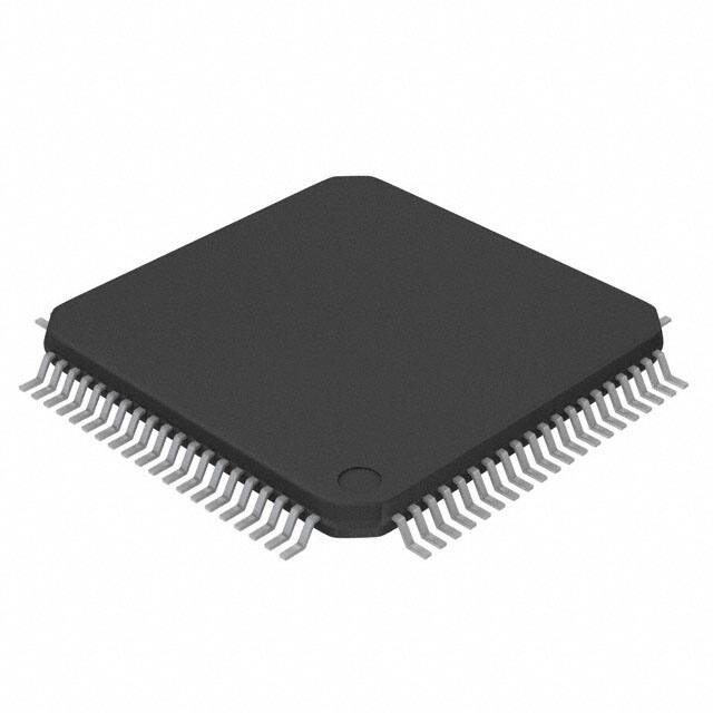
PFC Package
80-Pin TQFP
Top View
VSENSE14
1
60
EQ14
2
59
AUX6
AUX7
VSENSE13
3
58
V5VAO
FAULTH+
EQ13
4
57
VSENSE12
5
56
FAULTH-
EQ12
6
55
COMMH+
VSENSE11
7
54
COMMH-
EQ11
8
53
COMML-
VSENSE10
9
52
COMML+
FAULTL-
35
36
37
38
39
40
NC1
DG ND3
TX
RX
FAULT_ N
VIO
DG ND2
41
34
20
33
GPIO5
EQ5
CHM
42
VDIG
19
32
GPIO4
VSENSE5
CHP
GPIO3
43
31
44
18
30
17
EQ6
VM
VSENSE6
29
GPIO2
DGND1
45
VS ENSE0
16
28
GPIO1
EQ7
EQ1
46
27
15
26
GPIO0
VSENSE7
EQ2
CGND
47
VS ENSE1
48
14
25
13
EQ8
24
VSENSE8
VS ENSE2
WAKEUP
23
49
EQ3
12
VS ENSE3
FAULTL+
EQ9
22
50
21
51
11
EQ4
10
VS ENSE4
EQ10
VSENSE9
Pin Functions
NAME
4
TYPE
DESCRIPTION
PIN
NO.
AGND1
74
P
Analog Ground(2). Connect to ground plane.
AGND2
72
P
Analog Ground(2) for VREF. Internally shorted to AGND3, also make this connection externally in
the printed-circuit board (PCB) layout. Connect to ground plane.
AGND3
69
P
Analog Ground(2) for VREF. Internally shorted to AGND2, also make this connection externally in
the PCB layout. Connect to ground plane.
AUX0
66
AI
Ground referenced general-purpose analog measurement input.
AUX1
65
AI
Ground referenced general-purpose analog measurement input.
AUX2
64
AI
Ground referenced general-purpose analog measurement input.
AUX3
63
AI
Ground referenced general-purpose analog measurement input.
AUX4
62
AI
Ground referenced general-purpose analog measurement input.
AUX5
61
AI
Ground referenced general-purpose analog measurement input.
AUX6
60
AI
Ground referenced general-purpose analog measurement input.
AUX7
59
AI
Ground referenced general-purpose analog measurement input.
Submit Documentation Feedback
Copyright © 2015–2016, Texas Instruments Incorporated
Product Folder Links: bq76PL455A-Q1
�bq76PL455A-Q1
www.ti.com
SLUSC51C – APRIL 2015 – REVISED NOVEMBER 2016
Pin Functions (continued)
NAME
TYPE
DESCRIPTION
PIN
NO.
CGND
48
P
Communication ground(2). Connect to ground plane.
CHM
33
P
Charge pump flying capacitor connection. Connect a 22-nF ceramic capacitor(3) between this pin
and CHP.
CHP
32
P
Charge pump flying capacitor connection. Connect a 22-nF ceramic capacitor(3) between this pin
and CHM.
COMMH–
54
DIO
Inverting, high-side differential connection to the COMML– pin of the higher adjacent module in a
daisy chain.
Leave this pin unconnected if not used.
COMMH+
55
DIO
Non-inverting, high-side differential connection to the COMML+ pin of the higher adjacent module in
a daisy chain.
Leave this pin unconnected if not used.
COMML–
53
DIO
Inverting, low-side differential connection to the COMMH– pin of the lower adjacent module in a
daisy chain. Leave this pin unconnected if not used.
COMML+
52
DIO
Non-inverting, low-side differential connection to the COMMH+ pin of the lower adjacent module in a
daisy chain. Leave this pin unconnected if not used.
DGND1
30
P
Digital Ground(2). Connect to ground plane.
DGND2
35
P
Digital Ground(2). Connect to ground plane.
DGND3
37
P
Digital Ground(2). Connect to ground plane.
EQ1
28
DO
Cell Equalization control output used to drive an external N-FET balancing cell 1. May leave this pin
unconnected if not used.
EQ2
26
DO
Cell Equalization control output used to drive an external N-FET balancing cell 2. May leave this pin
unconnected if not used.
EQ3
24
DO
Cell Equalization control output used to drive an external N-FET balancing cell 3. May leave this pin
unconnected if not used.
EQ4
22
DO
Cell Equalization control output used to drive an external N-FET balancing cell 4. May leave this pin
unconnected if not used.
EQ5
20
DO
Cell Equalization control output used to drive an external N-FET balancing cell 5. May leave this pin
unconnected if not used.
EQ6
18
DO
Cell Equalization control output used to drive an external N-FET balancing cell 6. May leave this pin
unconnected if not used.
EQ7
16
DO
Cell Equalization control output used to drive an external N-FET balancing cell 7. May leave this pin
unconnected if not used.
EQ8
14
DO
Cell Equalization control output used to drive an external N-FET balancing cell 8. May leave this pin
unconnected if not used.
EQ9
12
DO
Cell Equalization control output used to drive an external N-FET balancing cell 9. May leave this pin
unconnected if not used.
EQ10
10
DO
Cell Equalization control output used to drive an external N-FET balancing cell 10. May leave this
pin unconnected if not used.
EQ11
8
DO
Cell Equalization control output used to drive an external N-FET balancing cell 11. May leave this
pin unconnected if not used.
EQ12
6
DO
Cell Equalization control output used to drive an external N-FET balancing cell 12. May leave this
pin unconnected if not used.
EQ13
4
DO
Cell Equalization control output used to drive an external N-FET balancing cell 13. May leave this
pin unconnected if not used.
EQ14
2
DO
Cell Equalization control output used to drive an external N-FET balancing cell 14. May leave this
pin unconnected if not used.
EQ15
80
DO
Cell Equalization control output used to drive an external N-FET balancing cell 15. May leave this
pin unconnected if not used.
EQ16
78
DO
Cell Equalization control output used to drive an external N-FET balancing cell 16. May leave this
pin unconnected if not used.
FAULT_N
40
DO
Single-ended active-low fault output. Leave this pin unconnected if not used.
FAULTH–
56
DI
Inverting, high-side differential connection to the FAULTL– pin of the higher adjacent module in a
daisy chain.
Leave this pin unconnected if not used.
Submit Documentation Feedback
Copyright © 2015–2016, Texas Instruments Incorporated
Product Folder Links: bq76PL455A-Q1
5
�bq76PL455A-Q1
SLUSC51C – APRIL 2015 – REVISED NOVEMBER 2016
www.ti.com
Pin Functions (continued)
NAME
TYPE
DESCRIPTION
57
DI
Non-inverting, high-side differential connection to the FAULTL+ pin of the higher adjacent module in
a daisy chain.
Leave this pin unconnected if not used.
FAULTL–
51
DO
Inverting, low-side differential connection to the FAULTH– pin of the lower adjacent module in a
daisy chain.
Leave this pin unconnected if not used.
FAULTL+
50
DO
Non-inverting, low-side differential connection to the FAULTH+ pin of the lower adjacent module in a
daisy chain.
Leave this pin unconnected if not used.
GPIO0
47
DIO
General Purpose I/O. Optionally use this pin as an external FAULT input or address assignment.
Do not allow GPIO pins to float when configured as inputs.
GPIO1
46
DIO
General Purpose I/O. Optionally use this pin as an external FAULT input or address assignment.
Do not allow GPIO pins to float when configured as inputs.
GPIO2
45
DIO
General Purpose I/O. Optionally use this pin as an external FAULT input or address assignment.
Do not allow GPIO pins to float when configured as inputs.
GPIO3
44
DIO
General Purpose I/O. Optionally use this pin as an external FAULT input or address assignment.
Do not allow GPIO pins to float when configured as inputs.
GPIO4
43
DIO
General Purpose I/O. Optionally use this pin as an external FAULT input or address assignment.
Do not allow GPIO pins to float when configured as inputs.
GPIO5
42
DIO
General Purpose I/O. Optionally use this pin as an external FAULT input.
Do not allow GPIO pins to float when configured as inputs.
NC1
36
NC
Do not connect to this pin. This pin must remain floating for correct operation.
NC2
75
NC
Do not connect to this pin. This pin must remain floating for correct operation.
NPNB
71
AO
Internal voltage regulator controller output pin. Connect to the base of the external NPN transistor.
Leave unconnected if not used.
OUT1
73
AO
Analog multiplexer output. Connect a 390-pF filter capacitor type C0G or NP0 between this pin and
AGND. Connect externally to pin OUT2. Internally tied to pin OUT2.
OUT2
68
AI
ADC input pin. Connect externally to pin OUT1. Internally tied to pin OUT1.
DI
Single-ended UART receive input. This pin must be either:
•
Driven from a UART signal OR
•
Pulled up to VIO
Do not allow this pin to float at any time.
Power supply input and module voltage-measurement pin. Connect to the top cell of the module
through a series resistor. Requires a decoupling capacitor(3) from TOP to the ground plane. See
TOP Pin Connection for details. Locate decoupling capacitor as close to pin as possible. The lowpass filter created by the RC should have a tau similar to the low-pass filter used in the VSENSE
circuits. See VP Regulated Output or Application and Implementation for component selection
details.
PIN
NO.
FAULTH+
RX
6
39
TOP
76
P
TX
38
DO
V5VAO
58
P
Connection to internal 5-V always-on supply. Decouple with a 4.7-µF capacitor(3) connected to the
ground plane. Locate decoupling capacitor as close to pin as possible. This pin should not be used
to supply external circuitry.
VDIG
34
P
5.3-V Digital Supply input. Always connect VDIG to VP with 1-Ω resistor. Decouple with 4.7-µF and
0.1-µF capacitors(3) in parallel to the ground plane. Locate decoupling capacitors as close to the
VDIG pin as possible.
Single-ended UART transmit output. Leave this pin unconnected if not used.
VIO
41
P
3-V to 5-V power input for IO supply. Connect this pin to the same power supply used to drive the
source/receiver for the GPIO, FAULT_N, RX, and TX pins. Typically, connect this pin to VP/VDIG
for all devices except the base device in the stack. In the base (or single) device, this pin is typically
driven from the same supply as the microcontroller I/O pins.
If VP/VDIG is connected as the power source, this pin should be decoupled with a 0.1-µF
capacitor(3) to the digital ground plane. Place a 1-Ω resistor in series from VP to VIO. Locate the
decoupling capacitor as close to the VIO pin as possible.
If another supply is used, decouple with parallel 10-µF and 0.1-µF capacitors(3).
VM
31
P
Internal –5-V charge pump output. Decouple with 4.7-µF and 0.1-µF capacitors(3) in parallel to the
ground plane. Locate decoupling capacitor as close to pin as possible.
Submit Documentation Feedback
Copyright © 2015–2016, Texas Instruments Incorporated
Product Folder Links: bq76PL455A-Q1
�bq76PL455A-Q1
www.ti.com
SLUSC51C – APRIL 2015 – REVISED NOVEMBER 2016
Pin Functions (continued)
NAME
PIN
NO.
TYPE
DESCRIPTION
VP
70
P
5.3-V regulated analog power supply input/sense pin.
Connect to external NPN transistor's emitter and decouple with a 0.1-µF capacitor(3) to AGND and a
4.7-µF capacitor(3) in series with a 0.390-Ω resistor to GND. Locate decoupling capacitors as close
to the VP pin as possible.
Always connect VDIG to VP with 1-Ω resistor.
VREF
67
P
VREF output filter pin. Decouple with parallel 0.1-µF and 1.8-µF (25 V+) capacitors(3) to the ground
plane. Locate decoupling capacitors as close to the pin as possible. To maintain measurement
fidelity, do not place external loads on this pin.
VSENSE0
29
AI
Connect to the negative pin of the 1st cell.
VSENSE1
27
AI
Channel 1. Connect to the positive pin of the 1st cell.
VSENSE2
25
AI
Channel 2. Connect to the positive pin of the 2nd cell.
VSENSE3
23
AI
Channel 3. Connect to the positive pin of the 3rd cell.
VSENSE4
21
AI
Channel 4. Connect to the positive pin of the 4th cell.
VSENSE5
19
AI
Channel 5. Connect to the positive pin of the 5th cell.
VSENSE6
17
AI
Channel 6. Connect to the positive pin of the 6th cell.
VSENSE7
15
AI
Channel 7. Connect to the positive pin of the 7th cell.
VSENSE8
13
AI
Channel 8. Connect to the positive pin of the 8th cell.
VSENSE9
11
AI
Channel 9. Connect to the positive pin of the 9th cell.
VSENSE10
9
AI
Channel 10. Connect to the positive pin of the 10th cell.
VSENSE11
7
AI
Channel 11. Connect to the positive pin of the 11th cell.
VSENSE12
5
AI
Channel 12.Connect to the positive pin of the 12th cell.
VSENSE13
3
AI
Channel 13. Connect to the positive pin of the 13th cell.
VSENSE14
1
AI
Channel 14. Connect to the positive pin of the 14th cell.
VSENSE15
79
AI
Channel 15. Connect to the positive pin of the 15th cell.
VSENSE16
77
AI
Channel 16. Connect to the positive pin of the 16th cell.
WAKEUP
49
DI
Wakeup input. Pull this pin low or tie to ground if not used. Do not allow this pin to float at any time.
(1) Key: AI = analog input; AO = analog output; DI = digital input; DO = digital output; DIO = digital I/O; P = Power; NC = no connect.
(2) Externally connected pins as common ground or GND in the design. See Grounding for details.
(3) All capacitors are type X7R or better, unless otherwise noted.
Submit Documentation Feedback
Copyright © 2015–2016, Texas Instruments Incorporated
Product Folder Links: bq76PL455A-Q1
7
�bq76PL455A-Q1
SLUSC51C – APRIL 2015 – REVISED NOVEMBER 2016
www.ti.com
6 Specifications
6.1 Absolute Maximum Ratings
over specified Ambient Temperature range (unless otherwise noted)
(1) (2)
MIN
MAX
UNIT
VP
–0.3
6
V
VDIG
–0.3
6
V
VIO
–0.3
6
V
Lesser of two MAX values
–0.3
6 or (VP + 0.3)
V
Lesser of two MAX values
–0.3
6 or (V5VAO + 0.3)
V
COMMH+, COMMH–, COMML+, COMMH–,
FAULTH+, FAULTH–, FAULTL+, FAULTL–
AC pulse specification (3) for these eight
pins only:
Vpk maximum ≤ 6.5 V for 100 ns or less,
100 kHz ≤ f ≤ 400 MHz
–0.3
6.5
Vpk
GPIO0–5
Lesser of two MAX values
–0.3
6 or (VIO + 0.3)
V
RX
Lesser of two MAX values
–0.3
6 or (VIO + 0.3)
V
–0.3
88
V
(VSENSE16 – 1 V)
(VSENSE16 + 5.5 V)
V
–0.3
0.3
V
n = 1 to 16
–0.3
5.5
n = 1 to 16, 0.1% duty cycle
–0.3
6.5
AUX0–7
TOP
(4)
(VSENSE16 + 5.5 V) ≥ TOP ≥
(VSENSE16 – 1 V)
TOP to VSENSE16 delta (4) (5)
VSENSE0
VSENSEn – VSENSEn–1
V
WAKEUP
–0.3
6
V
Ambient free-air temperature, TA
–40
105
⁰C
Junction temperature, TJ
–40
125
⁰C
Storage temperature, Tstg
–65
150
°C
(1)
(2)
(3)
(4)
(5)
Stresses beyond those listed under Absolute Maximum Ratings may cause permanent damage to the device. These are stress ratings
only, and functional operation of the device at these or any other conditions beyond those indicated under Recommended Operating
Conditions is not implied. Exposure to absolute-maximum-rated conditions for extended periods may affect device reliability.
Unless otherwise noted, voltages are given with respect to device commons (AGND1–3, DGND1–3, CGND) tied together (device VSS
or GND).
Specified by design, not tested in production.
Must meet all stated conditions for the TOP pin at all times.
Must short the highest-connected cell to the unused VSENSEn inputs above it in configurations that use < 16 cells. For example, a 14cell configuration must short pins VSENSE14, VSENSE15, VSENSE16.
6.2 ESD Ratings
VALUE
Human-body model (HBM), per AEC Q100-002 (1)
V(ESD)
(1)
8
Electrostatic discharge
Charged-device model (CDM), per AEC Q100-011
All pins
±2000
All pins except 1, 20, 21, 40, 41, 60, 61,
76, and 80
±500
Pin 76
±450
Corner pins (1, 20, 21, 40, 41, 60, 61,
and 80)
±750
UNIT
V
AEC Q100-002 indicates that HBM stressing shall be in accordance with the ANSI/ESDA/JEDEC JS-001 specification.
Submit Documentation Feedback
Copyright © 2015–2016, Texas Instruments Incorporated
Product Folder Links: bq76PL455A-Q1
�bq76PL455A-Q1
www.ti.com
SLUSC51C – APRIL 2015 – REVISED NOVEMBER 2016
6.3 Recommended Operating Conditions
TA = 25°C and TOP = 57.6 V; Min/Max values stated where TA = –40°C to 105⁰C and TOP = 12 V to 79.2 V (unless
otherwise noted)
MIN
VTOP
Supply voltage
VIO
Digital interface voltage
VTOP_DELTA
Max delta, TOP to highest cell
II/O
Output current, any one pin
GPIO0, GPIO1, GPIO2, GPIO3, GPIO4, GPIO5, TX,
FAULT_N
II/O_T
Output current, sum of
GPIO0 + GPIO1 + GPIO2 + GPIO3 + GPIO4 + GPIO5
+ TX + FAULT_N
(1)
(2)
TOP – GND (VSENSE16 = TOP)
(1) (2)
MAX
UNIT
12
NOM
79.2
V
2.7
5.5
V
300
mV
5
mA
20
mA
VSENSE16 – TOP
0
VSENSE input measurement accuracy is degraded when VTOP_DELTA is exceeded. Delta cannot exceed the limit in the Absolute Maximum
Ratings table.
Must short the highest-connected cell to the unused VSENSEn inputs above it in configurations that use < 16 cells. For example, a 14cell configuration must short pins VSENSE14, VSENSE15, and VSENSE16.
6.4 Thermal Information
bq76PL455A-Q1
THERMAL METRIC (1)
TQFP (PFC)
UNIT
80 PINS
RθJA, High K
Junction-to-ambient thermal resistance
44.3
°C/W
RθJC(top)
Junction-to-case (top) thermal resistance
6.4
°C/W
RθJB
Junction-to-board thermal resistance
21.5
°C/W
ψJT
Junction-to-top characterization parameter
0.2
°C/W
ψJB
Junction-to-board characterization parameter
21
°C/W
RθJC(bottom)
Junction-to-case (bottom) thermal resistance
—
°C/W
(1)
For more information about traditional and new thermal metrics, see the Semiconductor and IC Package Thermal Metrics application
report.
6.5 Electrical Characteristics: Supply Current (1)
The following applies to all Electrical Characteristics in the following tables, unless otherwise noted: TYP values are stated in
each table where VP = VDIG = 5.3 V, VIO = 5 V, TA = 25°C and VCELL = 3.6 V (VCELL= VSENSEn – VSENSEn–1; n=1 to 16),
TOP = 57.6 V. MIN/MAX values are stated where VP = VDIG = 5.3 V, VIO = 5 V, –40°C ≤ TA ≤ 85⁰C, 1 V < VCELL < 4.95 V,
12 V ≤ TOP < 79.2 V and GND = 0 V.
MIN
TYP
MAX
IIDLE
Total input current from the monitored
cells.
PARAMETER
Power state: IDLE (2)
4
5
7
mA
ITOP_IDLE
Input current into TOP pin, IDLE mode
Power state: IDLE (2)
250
350
450
µA
ISLEEP
Total input current from the monitored
cells into TOP pin
Power state: SHUTDOWN (3)
VP = VDIG = VIO = 0 V, TOP = 57.6
22
50
IACTIVE (4)
Total input current from the monitored
cells while communicating.
Power state: IDLE plus comms (5),
differential comm capacitance 70 pF, no
load on GPIO.
IVIO_IDLE
VIO input current
Power state: IDLE (2)
ISLP_DELTA (4)
Delta ISHUTDOWN between devices in a
stack
TA = 25°C ± 5°C for all devices
(1)
(2)
(3)
(4)
(5)
TEST CONDITIONS
UNIT
µA
8
mA
40
µA
4
10
µA
All internal pull-up and pull-down resistors are disabled and their current is not included in parameters listed in this table.
IDLE mode defined as: device awake, ready for communications, and not communicating.
SHUTDOWN mode defined as: test conditions, no communications, no wakeup tone activity, and no FAULT heartbeat.
Specified from characterization data.
ACTIVE mode defined as: UART, differential communications link, and FAULT heartbeat active.
Submit Documentation Feedback
Copyright © 2015–2016, Texas Instruments Incorporated
Product Folder Links: bq76PL455A-Q1
9
�bq76PL455A-Q1
SLUSC51C – APRIL 2015 – REVISED NOVEMBER 2016
www.ti.com
6.6 VP 5.3-V Supply Regulation Voltage
Characteristics stated using NPN transistor in circuit rated at BVCEO > 100V, β ≥ 100 at 5 mA, Base-Collector C ≤ 35 pF,
ICOLLECTOR > 100 mA, RCOLLECTOR = 400 Ω.
MIN
TYP
MAX
VPVR
Regulated Voltage
PARAMETER
5.1
5.3
5.5
INPNB
External NPN base drive current
0.5
VPSD_DLY
VP/VDIG delay before SHUTDOWN (1)
30
(1)
TEST CONDITIONS
UNIT
V
mA
75
160
ms
Time measured from VP falling below threshold until the part enters SHUTDOWN, or from the part attempting to exit SHUTDOWN
(wakeup) until re-entering SHUTDOWN.
6.7 VDD18 1.8-V Internal Digital Supply (1)
PARAMETER
VDD18VO
(1)
TEST CONDITIONS
VDD18 Output voltage (1)
As measured by internal ADC
MIN
TYP
MAX
1.7
1.8
1.9
UNIT
V
Internal node only, no external access. This parameter is for internal measurement and verification purposes only.
6.8 V5VAO Analog Supply
PARAMETER
TEST CONDITIONS
V5VAOSD
Output Voltage
Power state: SHUTDOWN,
VP = VDIG = VIO = 0 V
V5VAOIDLE
Output Voltage
Power state: IDLE (1), unloaded
(1)
MIN
TYP
MAX
4
4.7
5.3
V
VDIG
V
UNIT
VDIG – 0.5
UNIT
VDIG internally connected to V5VAO in IDLE mode.
6.9 VM –5-V Integrated Charge Pump
PARAMETER
TEST CONDITIONS
MIN
TYP
MAX
–5.5
–5
–4.5
VMVM_ON
VM Output Voltage
fCP
Charge pump switching frequency
375
kHz
VMTRIP
VM low-voltage monitor trip point
–3.8
V
VMVO
Measured value read back from ADC VM
monitor
–5.56
–5
–4.54
V
V
6.10 Analog-to-Digital Converter (ADC): Analog Front End
All ADC specifications stated are for the sampling intervals and register settings shown in Table 3. A 390-pF capacitor is on
pin OUT1.
PARAMETER
TEST CONDITIONS
MIN
OUT1RANGE
Pin OUT1 Analog Front End / Level
Shifter output voltage range
0
ROUT_PIN
OUT1 pin internal series resistance
1
10
Submit Documentation Feedback
TYP
1.2
MAX
UNIT
VP
V
1.35
kΩ
Copyright © 2015–2016, Texas Instruments Incorporated
Product Folder Links: bq76PL455A-Q1
�bq76PL455A-Q1
www.ti.com
SLUSC51C – APRIL 2015 – REVISED NOVEMBER 2016
6.11 ADC: VSENSEn Cell Measurement Inputs
PARAMETER
TEST CONDITIONS
VCELL_VR
Input voltage range
VCELL= VSENSEn – VSENSEn–1, n= 1
to 16
VCHERR25NB
Total Channel Measurement Accuracy at 25°C
VSENSE = 3.6 V
VCHERR
VCHERR
ISENSE_SEL(3)(4)
Total Channel Measurment Accuracy,
temperature range of 0°C to 65°C(1)(2)
TYP
1
MAX
UNIT
4.95
V
±0.75
mV
VSENSE = 1.5 V
–2.00
2.00
VSENSE = 2.0 V
–2.50
2.50
VSENSE = 3.3 V
–3.75
3.75
VSENSE = 3.6 V
–4.25
4.25
VSENSE = 4.2 V
–4.75
4.75
VSENSE = 4.5 V
–5.00
5.00
VSENSE = 1.5 V
–3.50
3.50
VSENSE = 2.0 V
–4.00
4.00
VSENSE = 3.3 V
–5.75
5.75
VSENSE = 3.6 V
–6.25
6.25
VSENSE = 4.2 V
–7.00
7.00
VSENSE = 4.5 V
–7.25
mV
Total Channel Measurment Accuracy,
temperature range of –40°C to 105°C(1)(2)
VSENSEn input current n = 1 to 16
MIN
mV
7.25
VSENSEn–1 pin; on selected channel
2
7.6
µA
ISENSE_NSEL
Channel not selected
< ±100
nA
ISENSE_SD
VSENSEn input current in
SHUTDOWN Mode
< ±100
nA
RSENSE_SEL(4)
VSENSE input resistance
Channel selected for conversion,
measured differentially
[VSENSEn–VSENSE(n–1)]
1
MΩ
OWDSR
Open-wire detection shunt resistance
Open-wire test mode, TSTCONFIG[4]
=1
all odd (CBENBL = 0xAA); or all even
(CBENBL=0x55) cell squeeze resistors
on (alternate resistors only)
LT_DriftVCHAN
Long-term drift (total channel path)
VADC_REF_25
ERRADC_REF_25
4
kΩ
VSENSE = 4.5 V, TA = 65°C(5)
18.47
VSENSE = 4.5 V, TA = 105°C(6)
50.24
ADC reference
ADC reference error
ppm/ 1000
hours
2.5
V
0°C ≤ TA ≤ 65°C
–3.5
3.5
mV
–40°C ≤ TA ≤ 105°C
–4.5
4.5
mV
(1) Error measured with averaging enabled.
(2) User adjustable Gain and Offset registers are provided for further error trim at VSGAIN and VSOFFSET, respectively.
(3) When the bq76PL455A is in IDLE power mode, but not converting any ADC input channel, the part idles the multiplexer on the highest
channel enabled for conversions in the CHAN register.
(4) The current into VSENSEn = ISENSE_SEL + VCELL/RSENSE_SEL.
(5) Computed from the first 500-hour operating life test at a stress temperature of 65°C.
(6) Computed from the first 500-hour operating life test at a stress temperature of 105°C.
6.12 ADC: VMODULE Input
PARAMETER
TEST CONDITIONS
VMODULE_VR
Input voltage range
Measured from TOP to GND (AGND1)
VMODULE_ERR105
Total error from all internal sources
TA = –40°C to 105°C
MIN
TYP
VTOP MIN
–650
MAX
UNIT
VTOP MAX
±100
650
Submit Documentation Feedback
Copyright © 2015–2016, Texas Instruments Incorporated
Product Folder Links: bq76PL455A-Q1
V
mV
11
�bq76PL455A-Q1
SLUSC51C – APRIL 2015 – REVISED NOVEMBER 2016
www.ti.com
6.13 ADC: Post Board Assembly(6): VSENSEn Cell Measurement Inputs
PARAMETER
VCELL_VR
TEST CONDITIONS
Input voltage range
VCHERR65NB
MIN
VCELL= VSENSEn – VSENSEn–1, n= 1
to 16
Total Channel Measurement Accuracy
in temperature range of 0°C to 65°C(1)(2)(3)
TYP
MAX
UNIT
V
1
4.95
VSENSE = 1.5 V
–3
3
VSENSE = 2.5 V
–3.5
3.5
VSENSE = 3.6 V
–5
5
VSENSE = 4.5 V
–7.6
7.6
VSENSE = 1.5 V
–4.5
4.5
VSENSE = 2.5 V
–6.3
6.3
VSENSE = 3.6 V
–8.4
8.4
VSENSE = 4.5 V
–11.
11.1
mV
VCHERR105NB
LT_DriftVCHAN
Total Channel Measurement Accuracy,
temperature range of –40°C to 105°C(1)(2)(3)
18.47
VSENSE = 4.5 V, TA = 65°C(4)
Long-term drift (total channel path)
ppm/ 1000
hours
50.24
(5)
VSENSE = 4.5 V, TA = 105°C
(1) Error measured with averaging enabled.
(2) User adjustable Gain and Offset registers are provided for further error trim at VSGAIN and VSOFFSET, respectively.
(3) Calculated and statistically projected worst case from characterization data. Includes inaccuracies due to IR reflow and thermal
hysteresis over 3 cycles (25°C -> –40°C -> 25°C -> 105°C -> 25°C)
(4) Computed from the first 500-hour operating life test at a stress temperature of 65°C.
(5) Computed from the first 500-hour operating life test at a stress temperature of 105°C.
(6) See Board Construction and Accuracy for board stack build information
6.14 ADC: AUXn General Purpose Inputs
PARAMETER
VAUX_VR
VAUXERR65
VAUXERR105
(1)
(2)
12
TEST CONDITIONS
Input voltage range (1)
VP/VDIG = 5.3 V
Total AUX Channel Measurement
Accuracy (2)
VAUX = 0.05 V, 0°C ≤ TA ≤ 65°C
Total AUX Channel Measurement
Accuracy (2)
MIN
TYP
0
MAX
UNIT
5
V
3
mV
–3
0.1
VAUX = 4.95 V, 0°C ≤ TA ≤ 65°C
–10
0.1
10
mV
VAUX = 0.05 V, –40°C ≤ TA ≤ 105°C
–4.5
0.1
4.5
mV
VAUX = 4.95 V, –40°C ≤ TA ≤ 105°C
–12.5
0.1
12.5
mV
Specified by design, not tested in production.
Calculated and statistically projected worst case from characterization data. Not tested in production.
Submit Documentation Feedback
Copyright © 2015–2016, Texas Instruments Incorporated
Product Folder Links: bq76PL455A-Q1
�bq76PL455A-Q1
www.ti.com
SLUSC51C – APRIL 2015 – REVISED NOVEMBER 2016
ADC: AUXn General Purpose Inputs (continued)
PARAMETER
IDCL_AUX
RIN_AUX
(1)
TEST CONDITIONS
DC Leakage Current
Channel not selected for conversion,
TESTAUXPU = 0
Equivalent input resistance
Channel selected In Acquisition Mode
CAUX (1)
Input capacitance
Channel selected
RAUX_PU
Internal switched pull-up resistor per
AUXn input, supplied from VP pin
TESTAUXPU[n] = 1; n = 0 to 7
MIN
18
TYP
MAX
UNIT
< ±0.1
µA
>3
MΩ
30
pF
26
46
kΩ
6.15 ADC: Internal Temperature Measurement and Thermal Shutdown (TSD)
PARAMETER
TEST CONDITIONS
MIN
TYP
MAX
UNIT
TINT_AD (1)
Internal temperature accuracy of analog
die
–7
3
13
°C
TINT_DD (1)
Internal temperature accuracy of digital
die
–34
8
54
°C
TSDT (2)
Thermal shutdown, junction temperature
both analog and digital dies
(1)
(2)
Increasing temperature
115
140
°C
Specified from characterization data, not tested in production.
Specified by design, not tested in production.
6.16 Passive Balancing Control Outputs
PARAMETER (1)
EQSR_OFF
MIN
TYP
MAX
EQn = 0 (OFF)
TEST CONDITIONS
1.2
1.5
1.8
UNIT
kΩ
EQn = 1 (ON)
1.9
2.3
2.9
kΩ
EQSR_ON
Output resistance, internally in series
with driver
EQVMIN (2)
Cell voltage required for balancing
1.8
V
VS1MIN
VSENSE1 minimum voltage for
balancing (3)
1.8
V
(1)
(2)
(3)
For more functional information, see Passive Balancing .
In the event of an open wire condition, if TSTCONFIG[EQ_SQUEEZE_EN] = 1 and this causes EQVMIN to be violated, it may be
necessary to power down the device to disable the squeeze resistor.
VSENSE1 minimum voltage required for correct operation of any or all EQn outputs. If VSENSE1 falls below this value, any or all other
EQ outputs may fail to assert when requested. The opposite is not true. Outputs will not assert unintentionally when set to the OFF
state.
6.17 Digital Input/Output: VIO-Based Single-Ended I/O
PARAMETER
TEST CONDITIONS
MIN
TYP
MAX
UNIT
VIO – 0.7
VIO
V
DGND
0.7
V
VOH
Logic-level output-voltage high
FAULT_N, TX, GPIO
ILOAD = 5 mA
VOL
Logic-level output-voltage low FAULT_N,
TX, GPIO
ILOAD = 5 mA
VIH
Logic-level input-voltage high RX, GPIO
VIL
Logic-level input-voltage low RX, GPIO
CDIG_IN
Input Capacitance (1) RX, GPIO
RPU
GPIO0..5 pull-up resistor
13
17
25
kΩ
RPD
GPIO0..5 pull-down resistor
16
22
31
kΩ
ILKG
Input leakage source/sink current RX,
GPIOx
RXTXBAUD
RX/TX signaling rate (2) (3)
ERRBAUD_RX
Input Baud rate error (1)
ERRBAUD_TX
Output Baud rate error (1)
tCOMM_BREAK
Communications Clear (Break) (1)
tCOMM_RESET
Communications Reset (1)
(1)
(2)
(3)
VIO – 0.7
V
0.7
V
5
pF
< ±1
µA
125
1000
–3%
3%
–1.5%
1.5%
10
15
Kbaud
bit periods
200
µs
Specified by design, not tested in production.
Defaults: RX = TX = 250 kBd at communications RESET or (factory set) EEPROM setting at POR.
Discrete rates only, not continuously variable.
Submit Documentation Feedback
Copyright © 2015–2016, Texas Instruments Incorporated
Product Folder Links: bq76PL455A-Q1
13
�bq76PL455A-Q1
SLUSC51C – APRIL 2015 – REVISED NOVEMBER 2016
www.ti.com
6.18 Digital Input/Output: Daisy Chain Vertical Bus
MAX
UNIT
VOH_DCC_TX
Logic level output voltage high
PARAMETER
Single driver loaded, ILOAD = 5 mA
TEST CONDITIONS
VDIG−1
VDIG
V
VOL_DCC_TX
Logic level output voltage low
Single driver loaded, ILOAD = 5 mA
GND
1
V
TPD
Internal propagation delay, COMML to
COMMH (1)
TDCC_BIT_TIME
Diff. Comms. Bit Time (1)
fWAKE_TONE
WAKE TONE frequency (1)
50% duty-cycle WAKE TONE
transmitted on differential pins
COMMH+/COMMH–
tWAKE
WAKE TONE duration (1)
WAKE TONE transmitted on differential
pins COMMH+/COMMH–
(1)
TONE
MIN
TYP
1.7 V] is
met.
1.2
ms
tWAKEUP_TO_DCOMM
Required delay from WAKETONE transmission
to ready for differential communications (3)
1.1
ms
tWAKEUP_TO_UART
Required delay from WAKETONE transmission
to ready for UART communications (3)
200
µs
(1)
(2)
(3)
2.3
UNIT
VIH_WAKEUP
V
0.7
100
V
µs
1.2
ms
Pulses shorter than 100 µs may wake the device, but must maintain 100 µs to assure start up.
Environmental noise may affect tone detection.
Specified by design, not tested in production.
6.20 EEPROM
over operating free-air temperature range (unless otherwise noted)
PARAMETER
EEPGM
(1)
EEPROM total program time
EECYCLES
Erase / Program cycles
EERETN
Data retention (2) (3)
(1)
(2)
(3)
TEST CONDITIONS
MIN
No writes to the device are allowed
during the programming cycle
(2)
TYP
MAX
UNIT
210
500
ms
(2)
5
10
cycles
years
Program EEPROM temperature (TA ) between 0°C and 30°C.
Specified by design, not tested in production.
Erase / Program cycles not to exceed EECYCLES.
6.21 Secondary Protector – Window Comparators
over operating free-air temperature range (unless otherwise noted)
PARAMETER
TEST CONDITIONS
OVRANGE
Over-voltage comparator register set-point
limits (1)
UVRANGE
Under-voltage comparator register set-point
limits (1)
OVUVSTEP
Threshold step resolution
ERRCMP_UV
Total UV threshold error (includes
ERRVCOMP_REF_45)
Vin = 0.7 to 3.875 V
ERRCMP_UV_EXT
UV threshold error when range-extend bit is set
COMP_UV[CMP_TST_SHF_UV] = 1
ERRCOMP_OV
Total OV threshold error (includes
ERRVCOMP_REF_45)
ERRCOMP_OV_EXT
OV threshold error when range-extend bit is set
Threshold hysteresis
VCOMP_HYST
(1)
14
MIN
TYP
2
0.7
MAX
UNIT
5.175
V
3.875
25
V
mV
–50
50
mV
–100
100
mV
Vin = 2 to 5.175 V
–50
50
mV
COMP_UV[CMP_TST_SHF_OV] = 1
–60
60
mV
Hysteresis enabled;
DEVCONFIG[COMP_HYST_EN] = 1
50
130
mV
85
Normal range specification. Ranges can be extended by using the COMP_UV[CMP_TST_SHF_UV] and
COMP_OV[CMP_TST_SHF_OV] bits. See register bit description in Table 7 for additional details.
Submit Documentation Feedback
Copyright © 2015–2016, Texas Instruments Incorporated
Product Folder Links: bq76PL455A-Q1
�bq76PL455A-Q1
www.ti.com
SLUSC51C – APRIL 2015 – REVISED NOVEMBER 2016
Secondary Protector – Window Comparators (continued)
over operating free-air temperature range (unless otherwise noted)
PARAMETER
TEST CONDITIONS
MIN
TYP
MAX
UNIT
TCOMP_UV
UVP Response time
Overdrive = 100 mV
20
µs
TCOMP_OV
OVP Response time
Overdrive = 100 mV
20
µs
VCOMP_REF_45
Comparator reference
Measured by ADC as HREF - HREF_GND
4.5
ERRVCOMP_REF_45
Comparator reference error
V
0°C ≤ TA ≤ 65°C, measured by ADC
–22
–7
9.5
mV
–40°C ≤ TA ≤ 85°C, measured by ADC
–27
–7
15
mV
MIN
TYP
MAX
Falling VP
4.3
4.5
4.7
Rising VP
4.3
4.5
4.7
6.22 Power-On-Reset (POR) and FAULT Flag Thresholds
PARAMETER
TEST CONDITIONS
VPFLT_TRIP
VP_FAULT voltage threshold, analog die
VMFLT_TRIP
VM_FAULT voltage threshold, analog die
DDIEPOR
VP/VDIG POR voltage threshold, digital
die
V5VAOSD
V5VAO SHUTDOWN voltage threshold,
digital die
VIOPOR
VIO POR voltage threshold, digital die
VIOSD_DLY
VIO delay before SHUTDOWN
Falling VM (more negative)
–4.2
–4
–3.8
Rising VM (more positive)
–3.9
–3.8
–3.7
Falling voltage, VP connected to VDIG
3.9
4.15
4.4
Rising voltage, VP connected to VDIG
4.1
4.5
4.7
Falling V5VAO
1.8
2.3
2.8
Rising V5VAO
UNIT
V
V
V
V
2.5
V
Falling VIO
2.1
2.3
2.5
Rising VIO
2.3
2.5
2.7
VIO ≤ VIOPOR
35
57
100
ms
MIN
TYP
MAX
UNIT
48
48.72
MHz
V
6.23 Miscellaneous
PARAMETER
TEST CONDITIONS
fOSC
Main oscillator frequency (±1.5%)
fHBEAT
Fault tone (heartbeat) frequency at pins
FAULTL±
No fault condition present, heartbeat
enabled
10
kHz
HBPULSE
Fault heartbeat pulse width at pins
FAULTL±
No fault condition present, heartbeat
enabled
125
ns
tCKSUM_USER
Time to complete User-space checksum
test (1)
5
ms
tCKSUM_TI
Time to complete TI-space checksum
test (1)
5
ms
tCKSUM_PER
Period for automatic checksum
updates (1)
2
(1)
tADCFullTest
Time to complete full ADC test
tADCTest
Time to complete abbreviated ADC
test (1)
VHREF_GND_FAUL
47.28
µs
450
ms
15
ms
Voltage threshold for 4.5-V reference
ground fault (1)
0.96
V
VHREF_FAULT_OV
Overvoltage threshold for 4.5-V
reference fault (1)
4.75
V
VHREF_FAULT_UV
Undervoltage threshold for 4.5-V
reference fault (1)
4.25
V
T
(1)
Specified by design, not tested in production.
Submit Documentation Feedback
Copyright © 2015–2016, Texas Instruments Incorporated
Product Folder Links: bq76PL455A-Q1
15
�bq76PL455A-Q1
SLUSC51C – APRIL 2015 – REVISED NOVEMBER 2016
www.ti.com
6.24 Typical Characteristics
The following conditions apply: Typical Operating Circuit, VTOP = 60 V, 16 cells, TA = 25°C (unless otherwise noted)
5
3
1.5 V
4
3.6 V
3
4.5 V
2
1
Error (mV)
Error (mV)
2
1
0
±1
0
±1
±2
±3
±2
±4
±5
±3
±40
±20
0
20
40
60
80
100
120
TA (ƒC)
1.0
1.5
2.0
2.5
3.0
3.5
4.0
4.5
Cell Voltage (V)
C001
Figure 1. Cell Voltage Measurement Error
Versus Ambient Temperature
5.0
C002
Figure 2. Cell Voltage Measurement Error
Versus Cell Voltage
3
2.0
1.5
2
1
0.5
Error (mV)
Error (mV)
1.0
0.0
±0.5
0
±1
±1.0
0.5 V
±1.5
±2
4.95 V
±2.0
±3
±40
±20
0
20
40
60
80
100
TA (ƒC)
120
1
2
3
4
5
AUX Voltage (V)
C004
Figure 4. AUX Measurement Error Versus AUX Voltage
30
30
28
28
26
26
24
24
Error (mV)
Error (mV)
Figure 3. AUX Measurement Error
Versus Ambient Temperature
22
20
18
22
20
18
16
16
14
14
12
12
10
10
±40
±20
0
20
40
60
80
100
TA (ƒC)
120
±40
±20
0
20
40
60
80
100
TA (ƒC)
C005
Figure 5. Overvoltage Comparator Error
Versus Ambient Temperature
16
0
C003
120
C006
Figure 6. Undervoltage Comparator Error
Versus Ambient Temperature
Submit Documentation Feedback
Copyright © 2015–2016, Texas Instruments Incorporated
Product Folder Links: bq76PL455A-Q1
�bq76PL455A-Q1
www.ti.com
SLUSC51C – APRIL 2015 – REVISED NOVEMBER 2016
Typical Characteristics (continued)
The following conditions apply: Typical Operating Circuit, VTOP = 60 V, 16 cells, TA = 25°C (unless otherwise noted)
30
30
16 V
80 V
Analog Die
Digital Die
20
10
Error (mV)
Error (mV)
10
0
±10
±30
±10
±50
±20
±70
±30
±90
±40
±20
0
20
40
60
80
100
TA (ƒC)
120
±40
±20
0
20
40
60
80
100
120
TA (ƒC)
C007
Figure 7. DIE Temperature Measurement Error
Versus Ambient Temperature
C008
Figure 8. Stack Measurement Error
Versus Ambient Temperature
50
30
40
25
30
20
ISLEEP ( A)
Error (mV)
20
10
0
±10
15
10
±20
±30
5
±40
0
±50
10
20
30
40
50
60
70
VSTACK (V)
80
±40
0
20
5
2.5012
4
2.5011
TA = 105°C
2.5013
2
60
80
100
120
C010
Figure 10. SLEEP Current Versus Ambient Temperature
6
3
40
TA (ƒC)
Figure 9. Stack Measurement Error Versus Stack Voltage
IACTIVE (mA)
±20
C009
2.501
2.5009
1
2.5008
0
±40
±20
0
20
40
60
TA (ƒC)
80
100
120
2.5007
0
C011
Figure 11. ACTIVE Current Versus Ambient Temperature
100
200
300
Time (hrs)
400
500
600
D001
Figure 12. ADC VREF Long Term Drift at 105°C
Submit Documentation Feedback
Copyright © 2015–2016, Texas Instruments Incorporated
Product Folder Links: bq76PL455A-Q1
17
�bq76PL455A-Q1
SLUSC51C – APRIL 2015 – REVISED NOVEMBER 2016
www.ti.com
7 Detailed Description
7.1 Overview
The bq76PL455A-Q1 is an integrated 16-cell monitor, protector, and cell balancer designed for high-reliability
automotive applications with many built-in self-diagnostic features.
Up to 16 bq76PL455A-Q1 devices can be connected in series using the high-speed differential communications
interface, which has been evaluated for compliance with Bulk Current Injection (BCI) standards. This capacitorisolated communications link provides effective common-mode noise rejection. The bq76PL455A-Q1
communicates with the host through a high-speed UART interface. The bq76PL455A-Q1 provides up to six
general-purpose, programmable, digital I/O ports, as well as eight AUX ADC inputs, typically used to monitor
externally supplied temperature sensors. Configuration of the digital I/O ports can be set to generate faults based
on conditions set in register GP_FLT_IN. Further configuration of these faults can be for an indication of a fault
on the FAULT_N output pin.
Designed for high-reliability automotive applications, the bq76PL455A-Q1 includes many functional blocks and
self-diagnostic test features covering defined single-fault conditions in analog and digital blocks. The host
microcontroller receives fault notifications through a separate communications path. The device contains userselectable self-test features to diagnose functional blocks within the device, such as automatic shutdown in the
event of overtemperature, calibration integrity, and so forth. The Safety Manual for bq76PL455A-Q1 (SLUUB67)
is available upon request for reference to aid the user in the evaluation of the built-in test features of the
bq76PL455A-Q1.
A provided built-in secondary protection block, with two dedicated programmable comparators per cell input,
separately senses and reports overvoltage and undervoltage conditions. The comparators utilize a second
separate testable internal band gap reference.
The bq76PL455A-Q1 provides pins for direct drive of external N-FETs for passive cell balancing with power
resistors. The balancing function configuration responds to on or off commands or specified to run for a specific
time.
The device is powered from the stack of cells to which it is connected and all required voltages are generated
internally.
18
Submit Documentation Feedback
Copyright © 2015–2016, Texas Instruments Incorporated
Product Folder Links: bq76PL455A-Q1
�bq76PL455A-Q1
www.ti.com
SLUSC51C – APRIL 2015 – REVISED NOVEMBER 2016
VREF
OUT2
V5VAO
OUT1
Charge
Pump
NPN PROTECT
VDIG
VP CLAMP
CHP
VM
VP
TOP
NPNB
HIGHEST
CELL
CHM
7.2 Functional Block Diagram
VREG1.8
2.5V
VREF
5.3 V REF
NPN Regulator
5V
ALWAYS
ON
10 V ALWAYS ON
VTOP
WinComp
Squeeze
Resistors
OV
Stack
Monitor
AGND
OSC
ADC
MUX
Temp
Sensor
VSENSE16
UV
ADC
POR
EQ16
VP POR
VP
OV
1k
VSENSE15
VDIG
VDIG POR
VIO
VIO POR
VDD18
1.8V POR
V5VAO
V5VAO POR
UV
Temp
Sensor
OV
AUX0
AFE
VSENSE2
AUX7
MUX
UV
AUX Pullup
EQ2
Control
AUXPUEN
OV
EEPROM
VSENSE1
V5VAO
UV
RX
EEC Decoder
EQ1
VSENSE0
TX
VDD18
EQ
Control
!
4.5V
VREF
Registers
V5VAO
TSD
VDIG
TX / RX
COMMH+
COMMH-
TX / RX
COMML+
COMML-
NPN PROTECT
OV DAC
UV DAC
!
WAKE
TSD
Threshold Set
VDIG
VDIG POR
VP
Digital
Comparators
WAKE
Checksum
Engine
WAKEUP
Control
POR
VM POR
VM
Wakeup
Control
FAULTH+
FAULTHFAULTL+
FAULTL-
WAKEUP
Comms
Interface
Registers
Registers
VP POR
LPF
I/O
WAKEUP
RX
GPIO5
GPIO0
FAULT_N
VIO
CGND
DGND
AGND3
AGND2
ANALOG DIE
AGND1
TX
DIGITAL DIE
Copyright © 2016, Texas Instruments Incorporated
7.3 Feature Description
7.3.1 Block Descriptions
7.3.1.1 Power
The bq76PL455A-Q1 operates from internally generated regulated voltages. The group of cells monitoring the
device is the source for the internal regulators. Power comes from the most-positive and most-negative pins of
the series-connected cells to minimize the likelihood of cell unbalancing. In most applications, the bq76PL455AQ1 operates using its internal supplies.
Submit Documentation Feedback
Copyright © 2015–2016, Texas Instruments Incorporated
Product Folder Links: bq76PL455A-Q1
19
�bq76PL455A-Q1
SLUSC51C – APRIL 2015 – REVISED NOVEMBER 2016
www.ti.com
Feature Description (continued)
12 to 79.2 V
NPNB
VDIG
VP
VIO
V10VAO
PRE-REGULATOR
(-) 8-16 CELL MODULE (+)
VP
REGULATOR
V5VAO
LDO
5.3 V VP RAIL
TOP
RX / TX
GPIO
FAULT_N
ANALOG DIE TSD
5.3 V VDIG RAIL
16 V EEPROM
CHARGE PUMP
VDIG_OK
V5VAO
DIGITAL DIE TSD
OSC
CHP
VREF
1.8 V
LDO
4.5 V
REF2
PROGRAM
2.5 V
VREF
VREF
VM
CHARGE PUMP
CHM
AFE
ADC
:,1'2: &203¶6
VM
DIGITAL CORE
LOGIC
GND
WAKEUP CIRCUITS
VBUS DRIVERS
VBUS RECEIVERS
DIGITAL DIE TSD
OSC
AFE
:,1'2: &203¶6
- ANALOG DIE
- DIGITAL DIE
EEPROM
:,1'2: &203¶6
OSC
ADC
1.8 V LDO
Partial diagram, some components omitted for clarity.
Inter-die connections not shown for clarity.
Refer to complete schematics (available from TI) for details.
Copyright © 2016, Texas Instruments Incorporated
Figure 13. Power Flow Diagram
20
Submit Documentation Feedback
Copyright © 2015–2016, Texas Instruments Incorporated
Product Folder Links: bq76PL455A-Q1
�bq76PL455A-Q1
www.ti.com
SLUSC51C – APRIL 2015 – REVISED NOVEMBER 2016
VDD18
VIO
VDIG
VP
VP Power Domain
V5VAO
Feature Description (continued)
POR
TSENSE
AUX[0..7]
VDIG
MUX
OUT2
ADC
VDD18
V5VAO
LDO
V5VAO (bypass cap)
VREF
(bypass cap)
VREF
VP
TSD
Level Shifters
VDIG
1.8 V LDO
VDD18
Power Domain
VDD18
OSC
V5VAO
POR OK
I/O
FAULTH
TX/
RX
FAULTL
TX/
RX
COMMH
TX/
RX
COMML
Level Shifters
Digital Control Logic
EEPROM
HVGEN
VDIG
Power
Domain
TX/
RX
Power-Up
Control
ANALOG die I/O
EEPROM
Programming
Voltage
+10 V (from ANALOG die)
LPR
WAKEUP
V5VAO
Power Domain
I/O
I/O
I/O
Low-Power
Receiver
KEY:
VP
GPIO
VIO Power Domain
VDIG
VDD18
VIO
GPIO[0..5]
FAULT_N
RX
TX
V5VAO
VIO
Copyright © 2016, Texas Instruments Incorporated
Figure 14. Digital Die Power Domains
Submit Documentation Feedback
Copyright © 2015–2016, Texas Instruments Incorporated
Product Folder Links: bq76PL455A-Q1
21
�bq76PL455A-Q1
SLUSC51C – APRIL 2015 – REVISED NOVEMBER 2016
www.ti.com
NPNB
VP
VDIG
CHM
CHP
VM
Feature Description (continued)
TOP
VP Power Domain
VSENSEn
VSENSEn-1
VMODULE
Measurement
VSENSE ...
Balancing
Control
Circuits
TOP
REF2
Cell
AFE/
Mux
VM
Power Domain
VM Monitor
Window Comparators
VM
VP
TSENSE
Control
Registers
VDIG
TOP
V10VAO
VDIG
CELLS 1-16
KEY:
LDO
TSD
V10VAO
Power Domain
VDIG Power Domain
Copyright © 2016, Texas Instruments Incorporated
Figure 15. Analog Die Power Domains
7.3.1.1.1 TOP Pin Connection
The bq76PL455A-Q1 has a connection from the top of the cell-module battery stack to the TOP pin, typically
through an external-series resistor and capacitor to GND forming a low-pass filter. The low-pass filter design
typically has a similar time constant to the VSENSE input pins. The minimum recommended values are 100 Ω
and 0.1 µF. See the Application and Implementation section for details.
7.3.1.1.2 V10VAO
V10VAO is an internal-only, always on, pre-regulator supplied from the TOP pin. It supplies the power to the
V5VAO block, Analog Die TSD block, and VP control and regulator circuits. It is not externally accessible.
7.3.1.1.3 V5VAO
V5VAO is the always-on power supply that ensures power is supplied to the differential communications circuits
(COMML+/–) and the WAKEUP input at all times. This ensures that the IC always detects the WAKEUP signal
and the differential communications receive the WAKE tone. The V5VAO is supplied by a combination of an
internal regulator and the VDIG supply. If VDIG falls below the normal operating voltage (during startup), the
internal regulator supplies V5VAO. Once VDIG reaches regulation, V5VAO is supplied directly from VDIG.
22
Submit Documentation Feedback
Copyright © 2015–2016, Texas Instruments Incorporated
Product Folder Links: bq76PL455A-Q1
�bq76PL455A-Q1
www.ti.com
SLUSC51C – APRIL 2015 – REVISED NOVEMBER 2016
Feature Description (continued)
NOTE
V5VAO can only supply enough power to meet internal IC requirements; it should not
connect to external circuitry.
7.3.1.1.4 VP Regulated Output
The bq76PL455A-Q1 power comes directly from the cells to which it is connected. Current draw is from the top
and bottom of the n-cell battery assembly, so that current through each cell is the same. An integrated linear
regulator utilizes an external NPN transistor (Zetex ZXTN4004K or similar) to generate a nominal 5.3-V rail on
pin VP. VP is both a power input and the sense node for this supply. The NPNB pin controls the external NPN
transistor of the regulator. A capacitor or resistor-capacitor combination must connect externally from VP to GND,
see Pin Configuration and Functions for details. VP must connect externally to VDIG and can optionally connect
to VIO. Both of these connections are through series 1-Ω resistors and separately decoupled. This regulator is
OFF in SHUTDOWN mode.
Table 1. Recommended NPN Transistor Characteristics
PARAMETER
BVCEO
DESCRIPTION
Collector-Emitter voltage
Beta β
Gain
CCB
Collector-Base capacitance
P
IC
(1)
(2)
Power handling
TEST CONDITION
TYPICAL VALUE
UNIT
100
V
at 5 mA
> 100
(1)
(2)
See the following text for
collector resistor details.
Collector current rating
≤ 35
pF
500
mW
> 100
mA
Choose this value with respect to the locally supplied maximum-cell voltage and derate appropriately for operating conditions and
temperature.
Derate this value appropriately for operating conditions and temperature.
Add a collector resistor between the NPN collector and the TOP pin to reduce power dissipation in the NPN
under normal and system fault conditions. The value of this resistor is chosen based on the minimum batterystack voltage, the bq76PL455A-Q1 VP/VDIG total load current, and the load current of any external I/O circuitry
powered directly or indirectly by VP/VDIG. Also, the recommendation is to add a 1-µF decoupling capacitor
directly from the collector to AGND.
7.3.1.1.5 VDIG Power Input
VDIG is the digital voltage supply input. Always connect it to the VP pin, which normally receives power from the
NPN. Optionally, an external supply may drive VDIG, but still must be connected to VP. This applies in all
operating modes. The VDIG source is from VP through a 1-Ω resistor. Decouple VDIG with a separate capacitor
at the pin.
7.3.1.1.6 VDD18 Regulator
A provided internal regulator generates a 1.8-V digital supply for internal device use only. The 1.8-V supply does
not require an external capacitor, and there is no pin or external connection. Faults on VDD18 that cause the
voltage to drop below its regulation may cause UART communication errors. If the fault is caused by LDO_TEST,
reset or shutdown/wakeup the device to regain functionality.
7.3.1.1.7 VIO Power Input
VIO is the voltage supply input used to power the digital I/O pins TX, RX, FAULT_N, and GPIOn. VIO may
connect to an externally regulated-supply rail, which is common to an I/O device such as a microcontroller.
Alternately, the source for VIO may be from VP through a 1-Ω resistor. Decouple VIO with a separate capacitor
at the pin.
If VIO does not have power, the part holds in reset and enters shutdown after a short delay. This gives a very
good reset mechanism for non-stacked systems. Upon power up from a SHUTDOWN, the
SHDN_STS[GTSD_PD_STAT] bit will be set. This flag bit is the logical of this condition or triggering the
thermal shutdown of the digital die in a die overtemperature situation.
Submit Documentation Feedback
Copyright © 2015–2016, Texas Instruments Incorporated
Product Folder Links: bq76PL455A-Q1
23
�bq76PL455A-Q1
SLUSC51C – APRIL 2015 – REVISED NOVEMBER 2016
www.ti.com
7.3.1.1.8 VM Charge Pump
The included internal-charge pump is for biasing the Analog Front End (AFE) and other analog circuits. It
requires an external flying capacitor connected between the CHP and CHM pins plus a storage capacitor on pin
VM to generate a rail of –5 V for internal use. The charge pump (VM) is always on in IDLE and off in
SHUTDOWN. VM requires the oscillator to be running and stable and does not start until the other supplies are
above their POR thresholds. The VM charge pump will start ramping at the start of the WAKEUP tone on COMH.
7.3.2 Analog Front End (AFE)/Level Shifter
The bq76PL455A-Q1 AFE allows monitoring of up to 16 cells. Provided for this purpose are seventeen VSENSE
inputs, labeled VSENSE0 through VSENSE16. The programming for bq76PL455A-Q1 can be set to sample all,
or a subset, of the connected cells. Sampling always begins at the highest-selected cell and finishes with the
lowest-selected cell. During measurement, the AFE selects the cell addressed by the logic block and level-shift
the sensed cell voltage with a gain of 1 down to the ground-referred OUT1 pin. The output of the AFE (OUT1)
has a See section '' for component selection.
The analog output of the AFE connects to OUT1 through an internal 1.2-kΩ series resistor. Connect OUT1
externally to OUT2. At this external connection between the AFE and the ADC, the requirement is to place an
external filter capacitor to form an RC filter to reduce noise bandwidth. A filter capacitor will increase the settling
time of the signal presented to the ADC input. A trade-off can be made between ADC sample time, filtering, and
accuracy. The AFE output must settle to within < 1/4 of the ADC LSB for best measurement accuracy.
7.3.3 ADC
The ADC in the bq76PL455A-Q1 is a 14-bit Successive Approximation Register (SAR) ADC. It has a fixed
conversion (hold) time of 3.44 µs, with a user-selectable sample interval or period between conversions. The
user-selectable sample interval determines the acquisition (tracking) settling time between conversions, used
mostly to allow the input capacitor on OUT1 to settle between conversions, and to allow for internal settling.
The ADC input mux on the digital die allows it to connect to the following:
• The AFE (analog die) mux output on OUT1 which measures:
– Up to 16 cell voltage channels
– The VMODULE voltage
– The internal temperature of the analog die
– The REF2 analog die reference
– The VM (–5V) charge pump generated voltage supply on the analog die
• Measurement channels on the digital die:
– The 8 AUX input channels
– The VDD18 1.8-V voltage supply on the digital die
– The internal temperature of the digital die
The ADC can be set up to take single samples or multiple samples in one of two averaging modes. This
selection is made using OVERSMPL[CMD_OVS_CYCLE].
7.3.3.1 Channel Selection Registers
Program channels for measurement by setting bits in the CHANNELS and NCHAN registers. Each channel can
be set up for measurement individually. User programmable correction factors are available for cell and AUX
channels. Conversion times are individually user programmable for different types of inputs (that is, cells, AUX,
and internal measurements).
The NCHAN register sets the number of VSENSE channels (cell inputs) for use by the device. Unused channels
are dropped consecutively starting from channel 16. Set this register for the number of cells used, that is, for 14
cells, program 0x0E. This register also sets mask cell overvoltage and undervoltage faults for unused channels,
and turns off the UV and OV comparators associated with the channel. The idle channel (the channel the mux
rests on between sample intervals) is set to the value in this register. This allows the OUT1 pin to hold the filter
capacitor at the voltage, which will be sampled first on the next cycle.
24
Submit Documentation Feedback
Copyright © 2015–2016, Texas Instruments Incorporated
Product Folder Links: bq76PL455A-Q1
�bq76PL455A-Q1
www.ti.com
SLUSC51C – APRIL 2015 – REVISED NOVEMBER 2016
7.3.3.2 Averaging
The oversampling for the ADC average measurements is programmable to 2, 4, 8, 16, or 32 times. Individual
samples are arithmetically averaged by the bq76PL455A-Q1, which then outputs a single 16-bit (14 bits + 2
additional bits created by the averaging process) average measurement. The individual samples used to create
the average value are not available.
As shown in Figure 16, the ADC averages any selected cell voltages first, then any selected AUX input channels,
and then any remaining channels selected in the CHANNELS register in the order listed. Depending on the state
of the CMD_OVS_CYCLE bit in the OVERSMPL register, oversampling of the Voltage and AUX channels follows
one of the following procedures:
• Sampling each channel once and cycling through all channels before oversampling again in the case of
CMD_OVS_CYCLE = 1 (cycled averaging) OR
• Sampling multiple times on a single channel before changing channel in the case of CMD_OVS_CYCLE = 0
(non-cycled averaging).
Figure 16 shows these on the left and right, respectively.
When oversampling, Table 2 shows the oversample periods for each channel after the first sample. The first
sample can have a different period programmed (see Table 2), followed by all subsequent samples at different
period shown in Table 3. The first sample and subsequent sample periods are separate of each other.
1
CMD_OVS_CYCLE = ?
0
Averaging?
VSENSE16
VSENSE16
Averaging?
VSENSE15
Averaging?
VSENSE15
Averaging?
VSENSE1
VSENSE1
AUX7
AUX7
Averaging?
Averaging?
Averaging?
AUX0
AUX0
Digital Die Temperature
Averaging is not available
for this node
Averaging?
Analog Die Temperature
Averaging?
Digital Die VDD18
Averaging?
Analog Die REF2
Averaging?
Analog Die REF2 GND
Averaging?
Analog Die VMODULE
(2 samples averaged per iteration)
Averaging?
Analog Die VM
Figure 16. Sampling/Oversampling (Averaging) Sequence
Submit Documentation Feedback
Copyright © 2015–2016, Texas Instruments Incorporated
Product Folder Links: bq76PL455A-Q1
25
�bq76PL455A-Q1
SLUSC51C – APRIL 2015 – REVISED NOVEMBER 2016
www.ti.com
Table 2. Channel Sample Period Settings
CHANNEL
(1)
(2)
OTHER SAMPLES (AVERAGING)
FIRST SAMPLE
CMD_OVS_CYCLE=0
CMD_OVS_CYCLE=1
VSENSEn (n=1..16)
ADC_PERIOD_VOL
CMD_OVS_HPER
ADC_PERIOD_VOL
AUXn (n=0..7)
ADC_PERIOD_AUXn
CMD_OVS_GPER
ADC_PERIOD_AUXn
DIGITAL DIE TEMP (1)
Approximately 50 µs
n/a
n/a
ANALOG DIE TEMP
ADC_PERIOD_TEMP
CMD_OVS_HPER
CMD_OVS_HPER
VDD18
Approximately 30 µs
CMD_OVS_GPER
CMD_OVS_GPER
ANALOG DIE VREF
ADC_PERIOD_REF
CMD_OVS_HPER
CMD_OVS_HPER
MODULE MONITOR (2)
ADC_PERIOD_MON
CMD_OVS_HPER
CMD_OVS_HPER
VM
ADC_PERIOD_VM
CMD_OVS_HPER
CMD_OVS_HPER
Oversampling (averaging) is not available for this measurement.
TSTCONFIG[MODULE_MON_EN] determines whether 2 conversions or 1 conversion takes place.
The ADC_PERIOD_VOL bits set the period between ADC samples for the indicated channels whether
oversampling or not. When CMD_OVS_CYCLE = 1, the oversampling period of the Cell and AUX channels
remains
fixed
at
the
single
sample
period
of
CELL_SPER[ADC_PERIOD_VOL]
and
AUX_SPER[ADC_PERIOD_AUX], respectively. Otherwise, if CMD_OVS_CYCLE = 0, then the oversample
period for the Cell channels is set by bits CMD_OVS_HPER and for the AUX channels is CMD_OVS_GPER.
CMD_OVS_HPER must be programmed to 12.6 µs and CMD_OVS_GPER can be programmed between 4.13
µs and 12.6 µs in the OVERSMPL register.
After the initial sample period performed per a single sample, oversampling on all other channels are at the
CMD_OVS_GPER and CMD_OVS_HPER period settings as indicated in Table 2.
Writing to the CMD register is used to start the voltage sampling process. This is usually done with a
BROADCAST Write_With_Response_Command sent to the CMD register. Using the BROADCAST version of
the synchronously sample channels command will result in all devices in the stack sampling at the same time.
That is, all devices begin sampling their respective cells, then AUX, and so on, simultaneously.
7.3.3.3 Recommended Sample Periods
Refer to Table 3 for initial recommended settings. Other settings are possible; see the Application and
Implementation section for additional information.
Table 3. ADC Recommended Sample Periods and Setup
MEASURED
PARAMETER
(2)
(3)
26
(1)
PERIOD REGISTER (2)
1 SAMPLE
SAMPLES 2–8
NAME
VCELL
60 µs
12.6 µs
CELL_SPER
0xBC
VAUX
12.6 µs
12.6 µs
AUX_SPER
0x44444444
VMODULE
1000 µs
12.6 µs
TEST_SPER
0xF999
Die Temp (ANL)
100 µs
12.6 µs
CELL_SPER
0xBC
Die Temp (DIG)
(1)
PERIOD
st
50 µs
(3)
AS SHIPPED
N/A
N/A
N/A
VM
30 µs
12.6 µs
TEST_SPER
0xF999
VDD18
30 µs
12.6 µs
N/A
N/A
REF2
30 µs
12.6 µs
TEST_SPER
0xF999
Sampling periods and averaging mode will affect device accuracy. Device accuracy and register settings (including the sampling period)
used to achieve stated device accuracy are specified under "Electrical Characteristics, ADC" in Analog-to-Digital Converter (ADC):
Analog Front End. Other settings are possible. Device accuracy is not assured at settings other than those specified in the Electrical
Characteristics tables.
Other register settings used: OVERSMPL = 0x7B; PWRCONFIG = 0x80
This is not a programmable parameter. No averaging is performed, but there is an inherent delay in the design for the ADC
measurement of the die temperature.
Submit Documentation Feedback
Copyright © 2015–2016, Texas Instruments Incorporated
Product Folder Links: bq76PL455A-Q1
�bq76PL455A-Q1
www.ti.com
SLUSC51C – APRIL 2015 – REVISED NOVEMBER 2016
7.3.3.4 VSENSE Input Channels
The VSENSE input channels measure the voltages of individual cells in the range of 1 V-to-4.95 V. Each input
should connect to an external low-pass filter (LPF) to reduce noise at the input, and a Zener diode to provide
protection to the device during random hot-plug cell connection. Typical values for the LPF range from 100 Ω to
1 kΩ, and 0.1 µF to 1 µF. Values outside this range may degrade accuracy due to system-level noise or from
excessive IR loss in the series resistor.
Tie up unused inputs to the highest-connected cell. For example, in a 14-cell system, tied to VSENSE14 are
unused inputs VSENSE15 and VSENSE16. Channels are used from lowest to highest, with VSENSE0
connected to the (–) terminal of the bottom cell.
The values returned from an ADC conversion for these channels convert to volts by:
VCELL = [(2 × VREF) / 65535] × READ_ADC_VALUE
(1)
A number of factors affect total channel measurement accuracy, including, but not limited to, variations due to IR
reflow, board-level stresses, any current leakage in external components, and the method of sampling. It is highly
recommended that the end user perform GAIN and OFFSET calibration as described in the Application and
Implementation section.
7.3.3.5 AUXn Input Channels
The AUXn input channels are used to measure external analog voltages from approximately 0 V to 5 V. A typical
use for these channels is to measure temperature using thermistors. These channels require a simple external
low-pass filter to reduce high frequency noise for best operation. The RC values correspond to the user's
application requirements.
The values returned from an ADC conversion for these channels convert to volts by:
VAUX = [(2 × VREF) / 65535] × READ_ADC_VALUE
(2)
7.3.3.6 VMODULE Measurement Result Conversion to Voltage
VMODULE is the voltage measured from the TOP pin to GND. The value scales by 25 with an internal resistor
voltage divider. Setting TSTCONFIG[MODULE_MON_EN] enables measuring of VMODULE voltage. Enable or
disable the measurement to aid with self-testing. When set to 0, the channel should measure close to 0 V.
The values returned from an ADC conversion for this channel converts to volts by:
VMODULE = ([(2 × VREF) / 65535] × READ_ADC_VALUE) × 25
(3)
7.3.3.7 Digital Die Temperature Measurement
The temperature of the digital die may be measured as a part of the normal ADC measurement sequence by
setting bit CHANNELS[CMD_TSEL]. The reported result is the voltage from the temperature sensor, not the
actual temperature.
No averaging is ever performed on this channel, but the timing will appear as if the requested oversampling was
performed.
FAULT_SYS[INT_TEMP_FAULT] is continuously updated based on the currently stored measurement result and
threshold. To allow clearing of the fault, sample the temperature within a normal operating range.
Conversion formula:
Internal Digital Die Temperature °C = (VADC – 2.287) × 131.944
(4)
7.3.3.7.1 Automatic Temperature Sampling
After initialization is complete, an internal timer will cause the digital-die temperature sensor sampling to be
scheduled once per second. No oversampling is performed. If a command or an auto-monitor cycle occurs that
samples the digital die temperature sensor, the timer resets. A command will interrupt an automatic temperature
sample, but if the command does not sample the digital die temperature, the automatic temperature sample will
occur as soon as the command completes. This can cause sample values to appear to change without a sample
request.
Submit Documentation Feedback
Copyright © 2015–2016, Texas Instruments Incorporated
Product Folder Links: bq76PL455A-Q1
27
�bq76PL455A-Q1
SLUSC51C – APRIL 2015 – REVISED NOVEMBER 2016
www.ti.com
7.3.3.8 Analog Die Temperature Measurement
The temperature measurement of the analog die is programmable as part of the normal ADC measurement
sequence by setting bit CHANNELS[CMD_HTSEL]. The reported result is the voltage from the temperature
sensor, not the actual temperature.
There is no internal threshold checking for this value. For self-testing purposes, the expectation is that the
microcontroller compares this value with the converted temperature from the digital die and decides if they are
reporting the same temperature. The analog die temperature measurement is more accurate than the digital-die
temperature measurement. Therefore, the digital die temperature measurement should be considered only a
rough estimation of the temperature measured by the analog die temperature monitor. The host firmware must
account for any offset between the two measurements.
Conversion formula:
Internal Analog Die Temperature °C = (VADC – 1.8078) × 147.514
where
•
VADC=[(2 × VREF) / 65535] × READ_ADC_VALUE
(5)
7.3.3.9 VM Measurement Result Conversion to Voltage
There is no internal threshold checking of this value. The expectation is that the microcontroller checks that the
value is within the appropriate range.
The value returned from an ADC conversion for this channel converts to volts by:
VVM = –2 × [(2 × VREF) / 65535] × READ_ADC_VALUE
(6)
7.3.3.10 V5VAO, VDIG, VDD18 Measurement Result Conversion to Voltage
The value returned from an ADC conversion for these channels converts to volts by:
VADC = [(2 × VREF) / 65535] × READ_ADC_VALUE
(7)
There is no internal threshold checking of these values. The expectation is that the microcontroller checks that
the values are within the appropriate ranges.
7.3.3.11 Auto-Monitor
Auto-monitor periodically samples a user-defined set of channels in the AM_CHAN register. The conversion
results do not automatically transmit on the communications channel, but are available to be read by the microcontroller. Auto-monitor senses non-masked fault conditions automatically without sending convert commands.
When Auto-monitor is running, the part is fully powered and awake in the IDLE state. Auto-monitor does not
affect operation of the secondary protection comparators.
Fault detection is fully functional and operates in the same manner as when Auto-monitor mode is not enabled.
NOTE
Always disable the Auto-monitor function before initiating any new action such as
requesting ADC samples, running checksum test, and so forth.
When enabled, Auto-monitor sets the STATUS[AUTO_MON_RUN] bit during the ADC conversion only.
Start the Auto-monitor function by setting AM_PER[AUTO_MON_PER] to a non-zero value. Setting the
STATUS[AUTO_MON_RUN] bit also restarts the Auto-monitor function when AM_PER[AUTO_MON_PER] is
non-zero. This can synchronize the Auto-monitor function measurement cycles to system operations and/or
between ICs in the stack.
28
Submit Documentation Feedback
Copyright © 2015–2016, Texas Instruments Incorporated
Product Folder Links: bq76PL455A-Q1
�bq76PL455A-Q1
www.ti.com
SLUSC51C – APRIL 2015 – REVISED NOVEMBER 2016
7.3.4 Thermal Shutdown
Thermal shutdown occurs when either one or both of the Thermal Shutdown (TSD) sensors on either die sense
an overtemperature condition. The sensors operate separately without interaction and are separate from the
analog and digital die sensors. Each has a separate register-status indicator flag. When a TSD fault occurs, the
part immediately enters the SHUTDOWN state. To awake the part, follow the normal WAKEUP procedure. The
bq76PL455A-Q1 does not exit SHUTDOWN automatically. It cannot be awakened until the temperature falls
below
the
TSD
threshold.
Upon
waking
up,
either
SHDN_STS[GTSD_PD_STAT]
or
(SHDN_STS[ANALOG_PD_STAT]&& SHDN_STS[HTSD_PD_STAT]) bits will be set.
7.3.5 Voltage Reference (ADC)
The VREF pin receives a precise internal voltage reference for the ADC. Two parallel X7R or better filter
capacitors between pins VREF and AGND are required for the reference; see Application and Implementation for
recommended values and PCB layout considerations.
7.3.6 Voltage Reference (REF2)
The window comparators have a 4.5-V internal voltage reference provided. It does not go out to an external pin.
To check the reference, select it with the CHANNELS[CMD_REFSEL] bit.
7.3.7 Passive Balancing
Sixteen internal drivers control individual cell balancing through the pins labeled EQ1…EQ16. When the device
issues a balance command through register CBENBL, the bq76PL455A-Q1 asserts the EQ(N) output, switches
to the VSENSE(N) rail and turns on QBAL. With a de-asserted register bit, the EQn bit switches to the
VSENSEn–1 rail, turns off QBAL, and reduces the balancing current to zero. The squeeze (OWD) function must
be disabled for correct balancing operation by setting TSTCONFIG[EQ_SQUEEZE_EN] = 0.
If CBCONFIG[BAL_CONTINUE] is set to '0', then when there is a FAULT the bq76PL455A-Q1 disables
balancing. The CBENBL register bits clear to indicate this event. However, there is one exception. The USER
checksum fault indicated by FALUT_DEV[USER_CKSUM_FLT] does not disable balancing. The following
describes the scenarios:
• BAL_CONTINUE = 0: CBENBL is set to 0 and balancing is disabled until the fault and fault status bits are
cleared. Information about what was being balanced is discarded. No change is made to the BAL_TIME bits
in CBCONFIG. The CBENBL register must then be rewritten with the desired balancing action.
• BAL_CONTINUE = 1: There is no effect on CBENBL and CBCONFIG and any balancing in progress
continues.
Changing the CBENBL register will create a checksum fault and cause FAULT_DEV[USER_CKSUM_ERR] to be
set. This may be a result of setting bits to enable balancing for cells, or the register being reset, because of a
fault or CBTIME expiring.
The internal balancing control circuitry only powers up when any bit in CBENBL is set. See Passive Cell
Balancing Circuit section for details on selecting the external passive balancing components.
7.3.8 General Purpose Input-Outputs (GPIO)
There are six GPIO pins available in the bq76PL455A-Q1. Registers GPIO_xxx, located at addresses 0x78–7D,
control GPIO behavior. Each can be programmed to be an input or output pin.
Each GPIO pin can have an internal pull-up or pull-down resistor enabled to keep the pin in a known state when
power is not on for external circuitry. Configuration for pull-up or pull-down resistors is in the GPIO_PU and
GPIO_PD registers. The pull-up/down resistors have internal connections to supply VIO. The resistor values are
in the Digital Input/Output: Wakeup section of the Electrical Characteristics tables.
The GPIOs can also trigger a FAULT condition. Programmed GPIOs trigger a FAULT indication by setting bits in
register GPIO_FLT_IN.
The FAULT_GPI register and the DEVCONFIG[UNLATCHED_FAULT] bit controls the behavior of the device in
response to a FAULT triggered by an enabled GPIO pin. The usual pin configuration is to be an input in the
GPIO_DIR register when used to trigger faults.
Submit Documentation Feedback
Copyright © 2015–2016, Texas Instruments Incorporated
Product Folder Links: bq76PL455A-Q1
29
�bq76PL455A-Q1
SLUSC51C – APRIL 2015 – REVISED NOVEMBER 2016
www.ti.com
7.3.9 UART Interface to Host Microcontroller
The UART follows the standard serial protocol of 8-N-1, where it sends information as a START bit, followed by
eight data bits, and then followed by one STOP bit. In all, 10 bits comprise a character time. Received data bits
are oversampled by 16 times to improve communication reliability.
The UART sends data on the TX pin and receives data on the RX pin. When the transmitter is idling (not sending
data), TX = 1. The RX input pin idles in the same state, RX = 1. Hold the RX line high using a pull-up to VIO, if
not used (that is, non-base device in the daisy chain). Do not allow the RX pin to float when VIO is present.
7.3.9.1 UART Transmitter
The transmitter can be configured to wait a specified amount of time after the last bit reception and start of
transmission using the TX_HOLDOFF register. The TX_HOLDOFF register specifies the number of bit periods
that the bq76PL455A-Q1 will wait to allow time for the microcontroller to switch the bus direction at the end of its
transmission.
7.3.9.2 UART Receiver
The UART interface design works in half-duplex. As a result, while the device is transmitting data on the TX pin,
it ignores RX. To avoid collisions when sending data up the daisy-chain interface, the host microcontroller should
wait until it receives all bytes of a transmission from the device to the microcontroller before attempting to send
data or commands up the daisy-chain interface. If the microcontroller starts a transaction without waiting to
receive the preceding transaction's response, the communication might hang up and the microcontroller may
need to send Communication Clear (see Communication Clear (Break) Detection) or Communication Reset (see
Communication Reset Detection) to restore normal communications.
7.3.9.3 Baud Rate Selection
The baud rate of the communications channel to the microcontroller is set in the COMCONFIG[BAUD] register
for 125k-250k-500k-1M baud rates. The default rate after a communications reset is 250k. The default rate after
a POR is the rate selected by the value stored in EEPROM for the COMCONFIG[BAUD] register.
When the value in this register changes, the new rate takes effect after the complete reception of a valid packet
containing the new setting including the CRC. This should send the next packet at the new baud rate and all
packets transmitted by the device will be at the new rate. It is possible to change the baud rate at any time and,
optionally, store the new baud rate in the EEPROM as a new POR default. After changing the baud rate, observe
a minimum wait period of 10 µs before sending the first packet at the new baud rate.
The value in the COMCONFIG[BAUD] register only affects the baud rate used in microcontroller communications
on the TX and RX pins. The daisy-chain vertical communication bus rate is at a higher fixed rate and not user
modifiable. All devices in the stack must have the same baud rate setting as the base device to read data from
stacked devices.
7.3.9.4 Communication Clear (Break) Detection
Use communications clear to reset the receiver to re-synchronize looking for the start of frame.
The receiver continuously monitors the RX line for a break () condition. A is detected when the
RX line is held low for at least tCOMM_BREAKmin bit periods (approximately 1 character times). Sending for more
than tCOMM_BREAKmax bit periods may result in recognition of a communication reset instead of the intended
communication clear. When detected, a will set the STATUS[COMM_CLEAR] flag.
7.3.9.5 Communication Reset Detection
Detection of a communication reset occurs when the RX line is held low for more than approximately
tCOMM_RESETmin. The primary purpose of sending a communications reset is to recover the device in the event the
baud rate is inadvertently changed or unknown. The baud rate resets unconditionally to the FACTORY default
value of 250 kb/s, REGARDLESS of the value stored in the EEPROM COMCONFIG register. This sets the baud
rate to a known, fixed rate (250k baud), and the STATUS[COMM_RESET] flag.
30
Submit Documentation Feedback
Copyright © 2015–2016, Texas Instruments Incorporated
Product Folder Links: bq76PL455A-Q1
�bq76PL455A-Q1
www.ti.com
SLUSC51C – APRIL 2015 – REVISED NOVEMBER 2016
7.3.9.6 Communication Timeouts
Programming is available for two timeout values based on the absence of a valid packet from either UART or
differential stack communications. The times are set in the two-bit fields of the Communications Timeout (CTO)
register. A valid packet definition is any packet with a valid CRC.
7.3.9.6.1 Communications Timeout Fault
Register CTO[COMM_TMOUT_PER] sets the period with no valid communications from either communications
interface before sensing a COMM_TIMEOUT fault.
Always set CTO[COMM_TMOUT_PER] to be set less than the CTO[COMM_PD_PER] to get a communications
timeout fault before SHUTDOWN occurs.
7.3.9.6.2 Communications Timeout Power-Down (SHUTDOWN)
CTO[COMM_PD_PER] forces the part to shut down when this time is exceeded without a valid communication
from either the UART or the differential stack communications.
7.3.10 Stacked Daisy-Chain Communications
In the stacked configuration, the main microcontroller first communicates through a bq76PL455A-Q1 device
using the UART communications interface, see Figure 17. Communication is then relayed up the chain of
connected slave bq76PL455A-Q1 devices using a proprietary differential communications protocol over ACcoupled differential links interconnected by the COMMH+/– and COMML+/– pins.
Each device in the daisy chain buffers the signal drive levels. The signal is not re-clocked or filtered; it passes
through the device without change and the entire stack sees all data sequencing regardless of the target device.
The packet is not validated before being transmitted to the next device in the daisy chain. The uniquely
addressed or group addressed device acts on the command (that is, begins an ADC conversion of the inputs) as
soon as it receives and validates the packet for correct address, message contents, and CRC.
Submit Documentation Feedback
Copyright © 2015–2016, Texas Instruments Incorporated
Product Folder Links: bq76PL455A-Q1
31
�bq76PL455A-Q1
FAULTHt
FAULTH+
COMMHt
www.ti.com
COMMH+
SLUSC51C – APRIL 2015 – REVISED NOVEMBER 2016
WAKEUP
WAKEUP
FAULTHt
FAULTLt
FAULT_N
FAULTH+
FAULTL+
FAULT_N
COMMHt
COMMLt
FAULTLt
COMML+
COMMH+
COMML+
FAULTL+
TX
TX
VIO
RX
COMMLt
VP
TWISTED PAIR WIRING
VP
RX
VIO
TWO CAPACITORS FOR
ENHANCED SAFETY
COMMH+
COMMHt
FAULTH+
FAULTHt
COMML+
COMMLt
FAULTL+
FAULTLt
DC BLOCKING CAPACITORS
(ISOLATION)
3.3 V / 5 V
LDO
TMS-570
MICROCONTROLLER
WAKEUP
GPIO_1
TX
RX
VDD
GPIO_0
RX
TX
VIO
FAULT_N
VP
Figure 17. Simplified Stack Communications Connectivity
7.3.10.1 Differential Communications
The bq76PL455A-Q1 uses two differential communications links, which perform different tasks. The hardware
used for the transmitters and receivers are similar. The communications link used for data and commands (the
vertical bus or VBUS) on the COMML+/– and COMMH+/– pairs is bidirectional, while the FAULTH+/– pins are
receivers only, and the FAULTL+/– are transmitters only.
NOTE
The UART receiver (RX), COMMH+/– transmitters, and COMML+/– receivers cannot be
disabled.
32
Submit Documentation Feedback
Copyright © 2015–2016, Texas Instruments Incorporated
Product Folder Links: bq76PL455A-Q1
�bq76PL455A-Q1
www.ti.com
SLUSC51C – APRIL 2015 – REVISED NOVEMBER 2016
The base device sends and receives data through UART at variable baud rates from 125 kb/s to 1 Mb/s. The
VBUS daisy chain operates at a fixed, nominal, data rate of 4 Mb/s using a proprietary asynchronous protocol.
Each byte is sent as 10 bits at 250 ns/bit or 2.5 µs/byte. The bottom device retransmits data from/to the
differential serial interface on the single-ended interface connected to the host system at the baud rate selected
for the single-ended serial interface. All bq76PL455A-Q1s in the daisy-chain should be set to the same baud rate
to align timing between the devices.
The VBUS interface uses a modified version of the UART protocol so it can easily translate to/from the UART
protocol. Transmission of a bit requires 250 ns, including both half-bits. It is effectively a 4-MHz signal that is
phase-shift keyed, so the resulting transmission will have both 4-MHz and 2-MHz components. See Figure 18 for
additional information.
7.3.10.2 Protocol Description
The differential VBUS uses an asynchronous byte-transfer protocol with one start bit, eight data bits, and an
optional framing bit. The start bit is always a zero. Duplication of the LSB-first data occurs so that the
transmission has no DC content. A zero is transmitted as one half-bit period low followed by one half-bit period
high. Transmission of a one is as one half-bit period high followed by one half-bit period low. A framing bit of one
will cause the byte to be discarded and the byte abort flag (FAULT_COM[ABORT_H or ABORT_L]) to be set.
Since the data transmit on the differential interface as it is being received from the single-ended UART interface,
this is used to indicate that an erroneous stop bit was detected.
Each time the bq76PL455A-Q1 detects a byte with a framing bit of zero, it is interpreted as a frame-initialization
byte. If the prior frame was not completed, FAULT_COM[FRAM_ERR] is set.
If detection of the start bit occurs, the receiver samples the input on the fourth clock edge to produce the bit.
Since a bit is always immediately followed by its complement, the two will be compared and the complement
error flag (FAULT_COM[COMP_ERR_H or COMP_ERR_L]) is set if they are not opposites. The first time such
an error occurs during a frame, the assumption is that the first sampling of the bit (not the complement) is the
correct one. (If this choice is incorrect, it should detect it as a CRC failure.) If such an error occurs more than
once during a frame, the fatal-complement error flag (FAULT_COM[COMP_FLT_H or COMP_FLT_L]) is set and
the frame ignored. Since the device ignores the remainder of the frame, a FRAM_ERR occurs when the next
frame arrives.
While receiving a byte, the receiver will resynchronize on every falling edge. A falling edge is expected at least
once every 3 bits. If the expected sampling point of the fourth bit does not detect a falling edge, the edge error
flag (FAULT_COM[EDGE_ERR_H or EDGE_ERR_L]) will be set and the receiver will return to idle, discarding
the frame.
If the bq76PL455A-Q1 device detects eight consecutive edge errors on the low-side interface (COMM_L+/–) with
no valid bytes being received, the block will be reset in the same manner as SOFT_RESET. This allows a
wakeup tone from the chip below in the stack to cause the part to reset.
125 ns
250 ns
COMM+
COMM–
rec_in
start
0
1
1
1
0
0
1
0
framing
Figure 18. VBUS Data Example, 0x4E Sent
Submit Documentation Feedback
Copyright © 2015–2016, Texas Instruments Incorporated
Product Folder Links: bq76PL455A-Q1
33
�bq76PL455A-Q1
SLUSC51C – APRIL 2015 – REVISED NOVEMBER 2016
www.ti.com
7.3.11 Register and EEPROM
7.3.11.1 Error Check and Correct (ECC) EEPROM
Register values for selected registers are permanently stored in EEPROM. All registers also exist as volatile
storage locations at the same addresses, referred to as shadow registers. The volatile registers are for reading,
writing, and device control. For a list of registers included in the EEPROM, see Table 7.
At wakeup, the bq76PL455A-Q1 first loads all shadow registers with default values from Register Summary.
Then the bq76PL455A-Q1 loads the registers conditionally with EEPROM contents from the results of the Error
Check and Correct (ECC) evaluation of the EEPROM.
The EEPROM is loaded to shadow registers in 64-bit blocks; each block has its own Error Check and Correct
(ECC) value stored. The ECC detects a single bit (Single-Error-Correction) or double bit (Double-Error-Detection)
changes in EEPROM stored data.
The ECC is calculated for each block, individually. Single-bit errors are corrected, double-bit errors are only
detected, not corrected. A block with good ECC is loaded. A block with a single-bit error is corrected, and either
FAULT_DEV[USER_ECC_COR] or FAULT_DEV[FACT_ECC_COR] bit is set to flag the corrected error event.
The block is loaded to shadow registers after the single-bit error correction. Since the evaluation is on a block-byblock basis, it is possible for multiple blocks to have a single-correctable error per block and still be loaded
correctly. Multiple bit errors can exist with full correction, as long as they are limited to a single error per block.
A block with a bad ECC comparison (two bit errors in one block) is not loaded and the
FAULT_DEV[USER_ECC_ERR] or FAULT_DEV[FACT_ECC_ERR] bit is set to flag the failed bit-error event.
The default value remains in the register. This allows some blocks to be loaded correctly (no fail or single bit
corrected value) and some blocks not to load. Any time either of the FAULT_DEV[*_ECC_ERR] is set, and the
condition is not cleared by a soft reset, the device has failed and should not be used.
7.3.12 FAULT Sensing and Signaling
A dedicated differential FAULT link allows each bq76PL455A-Q1 in a stack of devices to signal the presence of
any monitored and active/latched fault condition to the main microcontroller separately from the UART link. The
FAULTH+/– and FAULTL+/– pins implement an AC-coupled differential-signaling scheme similar to
communication pins COMML+/– and COMMH+/–, but using only a simple heartbeat signal to indicate normal or
fault conditions by the presence or absence of a repetitive pulse, respectively. The low duty-cycle heartbeat
stops anytime it senses a fault and the fault condition sets a bit in one of the FAULT_* registers. Masked faults
have no effect on the heartbeat generation.
34
Submit Documentation Feedback
Copyright © 2015–2016, Texas Instruments Incorporated
Product Folder Links: bq76PL455A-Q1
�bq76PL455A-Q1
www.ti.com
SLUSC51C – APRIL 2015 – REVISED NOVEMBER 2016
7.3.12.1 Fault Flow Schematics
FAULT MASKING
FAULT SOURCES
FAULT STATUS
MASK_COM[]
FAULT_COM[]
COMP_ERR_H_MSK
1
COMP_ERR_H_S
COMP_ERR_L_MSK
1
COMP_FLT_H_MSK
1
COMP_ERR_L_S
COMP_FLT_H_S
COMP_FLT_L_MSK
1
EDGE_ERR_H_MSK
1
COMP_FLT_L_S
EDGE_ERR_H_S
EDGE_ERR_L_MSK
1
ABORT_H_MSK
1
EDGE_ERR_L_S
&
COMP_ERR_H
&
COMP_ERR_L
&
COMP_FLT_H
&
COMP_FLT_L
&
EDGE_ERR_H
&
EDGE_ERR_L
&
ABORT_H
&
ABORT_L
&
CRC_FAULT_H
&
CRC_FAULT_L
&
FRAM_ERR
&
STOP_ERR
&
STK_FAULT_ERR
COMM_FAULT_ANY
ABORT_H_S
ABORT_L_MSK
1
CRC_FAULT_H_MSK
1
ABORT_L_S
CRC_FAULT_H_S
CRC_FAULT_L_MSK
1
FRAM_ERR_MSK
1
CRC_FAULT_L_S
FRAM_ERR_S
STOP_ERR_MSK
1
STK_FAULT_ERR_MSK
1
STOP_ERR_S
STK_FAULT_ERR_S
FAULT MASKING
FAULT SOURCES
H1
FAULT STATUS
MASK_DEV[]
FAULT_DEV[]
USER_CKSUM_MSK
1
USER_CKSUM_ERR_S
FACT_CKSUM_MSK
1
ANALOG_FERR_MSK
1
FACT_CKSUM_ERR_S
ANALOG_FAULT_ERR_S
&
USER_CKSUM_ERR
&
FACT_CKSUM_ERR
&
ANALOG_FAULT_ERR
HREF_FAULT_S
HREF_FAULT
HREF_GND_FAULT_S
HREF_GND_FAULT
CHIP_FAULT_ANY
H1
These faults are only
created on
command. They do
ADC_CAL_ERR_S
ADC_CAL_ERR
USER_ECC_COR_S
USER_ECC_COR
USER_ECC_ERR_S
USER_ECC_ERR
FACT_ECC_COR_S
FACT_ECC_COR
FACT_ECC_ERR_S
FACT_ECC_ERR
not require masks.
Legend
H1
PINx
X_ERR
&
Internal Source
1
External Source (pin)
P
H1
=1
P COMP_OV_THRESH
OV COMP
NCHAN[]
COMP_CONFIG < 2
&
COMP_OV_FAULT [15:0]
COMP_OV_FAULT _ANY
≥1
These UV and OV window comparator (WINCOMP) faults
only clear automatically when UNLATCHED _FAULT is set
and NO OTHER analog die based fault exists. This is true
even for faults that are masked.
COMP_OV[]
DAC
COMP_OV_THRESH[7:1]
Analog die faults include FAULT_SYS[3:0] or any bit in
registers FAULT _2UV[] or FAULT _2OV[].
REF2
FAULT SOURCES
FAULT MASKING
CELL_UV[]
VSENSEn
ADC
16
CELLn ADC RESULT [15 :0]
FAULT STATUS
FAULT _UV[]
P
VSENSEn-1
P< Q
UV_THRESH_CELL[15:0 ]
CELLn_UV_FAULT
UV_FAULT [15:0]
16
UV_FAULT _ANY
Q
≥1
UNLATCHED_FAULT
NCHAN[]
CELL0_OV[]
16
FAULT _UV[]
P
P> Q
OV_THRESH_CELL[15: 0]
CELLn_OV_FAULT
OV_FAULT[15:0]
16
OV_FAULT _ANY
Q
≥1
UNLATCHED_FAULT
NCHAN[]
Figure 20. Analog Faults
36
Submit Documentation Feedback
Copyright © 2015–2016, Texas Instruments Incorporated
Product Folder Links: bq76PL455A-Q1
�bq76PL455A-Q1
www.ti.com
SLUSC51C – APRIL 2015 – REVISED NOVEMBER 2016
FAULT SOURCES (8)
AUXn
ADC
FAULT MASKING
FAULT STATUS
AUX0_UV[]
FAULT_AUX[]
16
AUXn ADC RESULT [15:0]
P
PQ
AUXn_OV_FAULT
AUX_OV_FAULT [n]
Q
OV_THRESH_AUXn[15:0]
≥1
AUXOV_FLT_ANY
UNLATCHED _FAULT
FAULT SOURCES (6)
FAULT MASKING
FAULT STATUS
GPIO_IN[5:0]
GP_FLT_IN[]
FAULT_GPI[5:0]
GPIOn
GPIO_IN [n]
=1
n = 0:5
GPI_FLT_SENSE
&
GPI_FAULT [n ]
GPI_FLT_CONFIG[n]
≥1
GPI_FLT_ANY
UNLATCHED _FAULT
Figure 21. AUX and GPIO Pin Faults
FAULT MASKING
MASK_SYS[]
FAULT SOURCES
FAULT STATUS
FAULT_SYS[]
SYS_RESET_MSK
1
COMM _TIMEOUT_MSK
1
SYS _RESET_S
COMM_TIMEOUT_S
&
SYS_RESET
&
COMM _TIMEOUT
VDIG_WAKE_FAULT_S
INT_TEMP_FAULT _MSK
1
INT_TEMP_FAULT_S
VDIG_WAKE_FAULT
&
INT_TEMP_FAULT
SYS_FAULT _ANY
≥1
UNLATCHED_FAULT
VDIG_FAULT _MSK
1
VM_FAULT_MSK
1
VP_FAULT _MSK
1
VP_CLAMP_