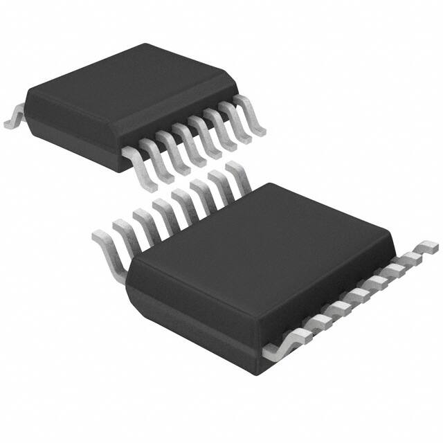
bq77PL157A4225
www.ti.com
SLUSA00B – MARCH 2010 – REVISED APRIL 2012
Voltage Protection for 3-Series to 6-Series Cell Lithium-Ion/Polymer Batteries
Check for Samples: bq77PL157A4225
FEATURES
1
•
•
•
•
•
•
•
•
•
•
Single IC Li-Ion Protection for 3-Series to 6Series Cells
Stackable to Protect up to 18-Series Cells
Programmable Detection Time Delay
Low Power Consumption
– Typical 2-µA to 2.5-µA Normal Mode
Fixed 4.225 V Overvoltage Threshold
Highly Accurate: ±20-mV MAX, TA = 0°C to
50°C
Output Activation for Low Side FET
(Contact TI for Alternate Output Options:
High/Low-side Fuse or FET)
Protected Output, Power, and Ground Pins for
Added Safety and Reliability
Permanent or Recoverable Fault Options
16-pin Small Outline Package
APPLICATIONS
•
Primary or Secondary Level Voltage Protection
for Li-Ion Battery Packs for Use in:
– Power Tools
– UPS Systems
– E-Bikes, Scooters, and Small Mobility
Vehicles
– Medical Devices, Test Equipment, and
Industrial Products
DESCRIPTION
The bq77PL157 is a stackable overvoltage protection
device for 3, 4, 5 or 6 series cell Li-Ion battery packs.
This device incorporates a precise and accurate
overvoltage detection circuit with preconfigured
threshold limits. Additional features include the ability
to stack multiple parts to monitor up to 18 series
cells.
FUNCTION
Each series cell in a Li-Ion battery pack is compared
to an internal reference voltage. If one cell reaches
an overvoltage condition, the protection sequence
begins. The bq77PL157 starts charging an external
capacitor through the CD pin. When the CD pin
voltage reaches 1.2 V, the OUT pin changes state
and the LVO pin becomes active.
If multiple bq77PL157 devices are stacked, the LVIN
pin of the next-lower device receives the LVO pin
from the above device and similarly starts a
shortened delay timer before activating its OUT pin.
(No additional isolation or level-shift circuitry is
required.) The lowest bq77PL157 in the string is used
to activate a power MOSFET located in the low side
of the power path.
1
Please be aware that an important notice concerning availability, standard warranty, and use in critical applications of
Texas Instruments semiconductor products and disclaimers thereto appears at the end of this data sheet.
PRODUCTION DATA information is current as of publication date.
Products conform to specifications per the terms of the Texas
Instruments standard warranty. Production processing does not
necessarily include testing of all parameters.
Copyright © 2010–2012, Texas Instruments Incorporated
�bq77PL157A4225
SLUSA00B – MARCH 2010 – REVISED APRIL 2012
www.ti.com
These devices have limited built-in ESD protection. The leads should be shorted together or the device placed in conductive foam
during storage or handling to prevent electrostatic damage to the MOS gates.
ORDERING INFORMATION
VPROTECT
4.225 V
DEVICE
FEATURE CONFIGURATION
bq77PL157A
Recoverable Output
PACKAGING
FULL PART NAME
Tape and Reel
bq77PL157APWR-4225
Tube
bq77PL157APW-4225
DEVICE INFORMATION
PW PACKAGE
(TOP VIEW)
LVO
1
16
LVIN
VC1
2
15
NC
VC2
3
14
CD
VC3
4
13
VDD
VC4
5
12
PCKP
VC5
6
11
NC
VC6
7
10
OUT
GND
8
9
PCKN
bq77PL157
Low-Side
CHG FET
PIN FUNCTIONS
2
PIN NAME
PIN NO.
CD
14
External capacitor to GND to set delay time
DESCRIPTION
GND
8
Ground pin and negative end of cell stack
LVIN
16
Level-shift input (used for stacking, input is from next-higher part)
LVO
1
Level-shift output (used for stacking, route this output to next-lower part)
NC
11, 15
No connection
OUT
10
Output gate drive to external MOSFET
PCKN
9
Pack negative supply for OUT driver (connect to source of external MOSFET or GND if device not at
bottom of stack)
PCKP
12
Pack positive supply for OUT driver (connect to most positive cell input of device)
VC1
2
Sense voltage input for most positive cell
VC2
3
Sense voltage input for second most positive cell
VC3
4
Sense voltage input for third most positive cell
VC4
5
Sense voltage input for fourth most positive cell
VC5
6
Sense voltage input for fifth most positive cell
VC6
7
Sense voltage input for least positive cell
VDD
13
Power supply (via RC filter)
Copyright © 2010–2012, Texas Instruments Incorporated
�bq77PL157A4225
www.ti.com
SLUSA00B – MARCH 2010 – REVISED APRIL 2012
FUNCTIONAL BLOCK DIAGRAMS
RVDD
LVIN
R IN
VDD
PACK+
C VDD
PCKP
VC1
C IN
R IN
Level
shifter
VC2
C IN
R IN
VC3
x10
ICD = 0.2 µA (TYP)
C IN
R IN
VC4
C IN
R IN
Timer
Control
VC5
OUT
C IN
R IN
0.2 µA
(TYP)
VC6
1.2V(TYP)
Level
shifter
C IN
GND
PCKN
CD
CCD
LVO
PACKNMOS
Figure 1. bq77PL157 – Low-Side Power NMOS Direct-Drive Output
ABSOLUTE MAXIMUM RATINGS
over recommended operating free-air temperature range, (unless otherwise noted) (1)
RANGE
Supply voltage range, VMAX
VDD, PCKP
PCKN
VCn (n=1 to 6)
Input voltage range, VIN
Output voltage range, VOUT
(VDD – 50) to VSS + 35 V
–0.3 to 35 V
VCn – VC(n+1), (n=1 to 5), VC6–GND
–0.3 to 8 V
LVIN
–0.3 to 35 V
OUT
–0.3 to 35 V
CD
–0.3 to 35 V
LVO
Storage temperature range, Tstg
(1)
–0.3 to 35 V
–0.3 to 35 V
–65°C to 150°C
Stresses beyond those listed under absolute maximum ratings may cause permanent damage to the device. These are stress ratings
only and functional operation of the device at these or any other conditions beyond those indicated under recommended operating
conditions is not implied. Exposure to absolute–maximum–rated conditions for extended periods may affect device reliability.
Copyright © 2010–2012, Texas Instruments Incorporated
3
�bq77PL157A4225
SLUSA00B – MARCH 2010 – REVISED APRIL 2012
www.ti.com
RECOMMENDED OPERATING CONDITIONS
over operating free-air temperature range (unless otherwise noted)
MIN
TYP
MAX
UNIT
Supply voltage
VDD
4.2
30
V
Pack positive voltage
PCKP
0
30
V
Pack negative voltage
PCKN
VDD – 30
30
V
VCn (n = 1 to 6)
0
VDD
VCn – VC(n + 1), (n = 1 to 5) VC6–GND
0
5
Input voltage range
Delay time capacitor
CCD
Voltage monitor filter resistance
RIN
Voltage monitor filter capacitance
CIN
Supply voltage filter resistance
RVDD
Supply voltage filter capacitance
CVDD
0.22
µF
1
kΩ
0.01
0.1
µF
0
1
kΩ
0.1
Operating ambient temperature range, TA
V
–40
µF
110
°C
ELECTRICAL CHARACTERISTICS
over recommended operating free-air temperature range (unless otherwise noted), typical values stated where TA = 25°C
PARAMETER
VOA
Overvoltage detection accuracy
VPROTECT
Overvoltage detection voltage
VTH
Overvoltage detection hysteresis
TYP
MAX
TA = 0°C to 50°C
TEST CONDITION
MIN
±5
±25
TA = –20°C to 85°C
±5
±40
TA = –40°C to 110°C
±5
±70
4.225
150
UNIT
mV
V
450
mV
±0.2
µA
1
1.5
µA
1
1.5
2
s
0.7
1.5
2.3
s
Input current on VCn (n = 2 to 6),
VCn – VC(n + 1), (n = 1 to 5),
VC6 – GND = VPROTECT – 25 mV
Input current on VC1 (2)
VCn – VC(n + 1), (n = 1 to 5),
VC6 – GND = VPROTECT – 3.5 V
tD
Overvoltage detection delay time
VCn – VC(n+1), (n=1 to 5),
VC6 – GND = VPROTECT + 25 mV, VDD = VC1
CD = 0.22 µF
tOA
Minimum output active (fault) time
VCn – VC(n + 1), (n = 1 to 5),
VC6 – GND = VPROTECT – VTH,
VDD = VC1, CD = 0.22 µF
VCD,TH1
CD threshold voltage for output transition
from inactive (no fault) to active (fault)
1.2
V
VCD,TH2
CD clamp voltage after output change to
active (fault)
2.4
V
ICH1
CD charge current by overvoltage
CD voltage = GND to VCD,TH1
ICH2
CD clamp current after output active
CD voltage = VCD,TH1 to VCD,TH2
IDS1
CD discharge current
CD voltage = VCD,TH2 to VCD,TH1
IDS2
CD clamp current
CD voltage = VCD,TH1 to GND
IDD
VDD Supply current
All cell voltages at 3.5 V/cell
IPCKP
Output supply current
PCKP = 22 V
IIN
(1)
(2)
4
(1)
VCn – VC(n+1), (n=1 to 5),
VC6-GND = VPROTECT + 25 mV
VDD = VC1
VCn – VC(n + 1), (n = 1 to 5),
VC6 – GND = VPROTECT – VTH,
VDD = VC1
Before output active
CD = GND
After output active
CD = VCD,TH1
After OUT active
and CD reaches
VCD,TH2
CD = VCD,TH2
After OUT inactive,
CD = VCD, TH1
–0.1
–0.2
–0.3
µA
1
2
3
µA
0.1
0.2
0.3
µA
90
µA
2
3.5
µA
0.4
0.8
µA
Input current of each VCx does not include IDD current of VDD.
Input current from top cell does not contribute to cell imbalance.
Copyright © 2010–2012, Texas Instruments Incorporated
�bq77PL157A4225
www.ti.com
SLUSA00B – MARCH 2010 – REVISED APRIL 2012
VPROTECT
V
PROTECT-
Cell Voltage
(VCn - VC(n-1),
(VC6 - GND)
2.4 V
I CH2
I DS1
1.2 V
I CH1
I CH1
VTH
I DS2
I DS2
CD
Figure 2. CD charge Current and Discharge Current
bq77PL157 OUTPUT
PARAMETER
VOUT OUT pin drive voltage
TEST CONDITION
MIN
TYP
VCn – VC(n + 1), (n =1 to 5), VC6 – GND =
VPROTECT + 25 mV, VDD = VC1, IOUT = 0 to –0.1
mA, TA = –40°C to 110°C
VCn – VC(n + 1), (n = 1 to 5), VC6 – GND =
VPROTECT – 25 mV, VDD = VC1, IOUT = 0 to 0.1 mA,
TA = –40°C to 110°C
MAX
UNIT
PCKN + 0.2
V
PCKN + 9
PCKN + 14
PCKN + 16
VOUT rise time
CL = 5000 pF, VOUT: 10% to 90%
100
µs
VOUT fall time
CL = 5000 pF, VOUT: 90% to 10%
100
µs
LEVEL SHIFT FUNCTION
PARAMETER
ILVL
LVIN pull down current
VLVL
LVIN threshold voltage
VOH
LVO output high voltage
tDA
Output-active time-delay
time
ICHLV
CD charge current by
LVIN input
tDIA
IDSLV
TEST CONDITION
VCn – VC(n + 1), (n = 1 to 5), VC6 –GND =
VPROTECT – 25 mV, VDD = VC1, LVIN = VDD + 4 V
IOH = –7 µA
VCn – VC(n + 1), (n = 1 to 5),
VC6 – GND = VPROTECT –25 mV,
LVIN = VDD + 4 V
CCD = 0.22 µF
Output-inactive delay time VCn – VC(n + 1), (n = 1 to 5),
VC6 – GND = VPROTECT –25 mV,
CD charge current by
LVIN = VDD
LVIN input
CCD = 0.22 µF
Copyright © 2010–2012, Texas Instruments Incorporated
CD = GND
CD = GND
MIN
TYP
MAX
UNIT
2
3.8
7
µA
VDD + 1
VDD + 3.5
V
GND + 4
GND + 6
V
132
9 × ICH2
10 × ICH2
ms
11 × ICH2
3.5
IDS2
IDS2
µA
ms
IDS2
µA
5
�bq77PL157A4225
SLUSA00B – MARCH 2010 – REVISED APRIL 2012
www.ti.com
H
VLVL
LVIN
2.4 V
IDSLV
ICH2
1.2V
IDS2
ICHLV
CD
Figure 3. CD Charge Current and Discharge Current
I CC
1
16
I IN
2
VC1
15
I IN
3
VC2
14
I IN
4
VC3
VDD
13
I IN
5
VC4
PCKP
12
I IN
6
VC5
11
I IN
7
VC6
10
8
GND
9
Figure 4. ICC, IIN Measurement Test Setup
OPERATION AND TIMING OF PROTECTION OUTPUT
From Direct Cell Inputs
When any one of the cell voltages exceeds VPROTECT, an internal current source begins to charge capacitor CCD
connected to the CD pin, which acts as a delay timer. If all cell voltages fall below VPROTECT before VCD reaches
VCD,TH1, the delay timer is reset and the OUT pin is not activated (i.e., no fault detected, output remains
unchanged). An internal switch clamps the CD pin to GND, discharges the capacitor CCD, and resets the full
delay time for the next occurring overvoltage event.
If any cell voltage exceeds VPROTECT long enough for the voltage at the CD pin (VCD) to reach VCD,TH1 (1.2 V
typical), then the OUT and LVO pins are activated (i.e., fault detected, output changes state), thus interrupting
the circuit via the FET protection device. Once the output is activated, the CD pin is charged up to its maximum
value VCD,TH2 (2.4 V typical).
6
Copyright © 2010–2012, Texas Instruments Incorporated
�bq77PL157A4225
www.ti.com
SLUSA00B – MARCH 2010 – REVISED APRIL 2012
When the recovery option is selected, if all cell voltages fall below VPROTECT – VTH (threshold hysteresis), an
internal current source begins to discharge capacitor CCD, also acting as a delay timer. If any cell voltage returns
back above VPROTECT – VTH before VCD reaches VCD,TH1, the delay timer is reset and the OUT and LVO pins
remains active (i.e. in the fault state). The CD pin is charged back to its maximum value VCD,TH2.
If all cell voltages remain below VPROTECT – VTH long enough for the voltage at the CD pin to reach VCD,TH1, then
the OUT and LVO pins are deactivated (i.e. output returns to the no fault state). An internal switch clamps the
CD pin to GND, discharges the capacitor CCD, and resets the full delay time for the next occurring overvoltage
event.
The delay time for detecting an overvoltage fault is the time between charging CCD from 0 to VCD,TH1 and can be
calculated as follows:
tD = (VCD,TH1 × CCD) / ICH1
CCD = (tD × ICH1) / VCD,TH1
where ICH1 = CD charge current = 0.2 µA (typical)
The recovery delay time is the time between discharging from VCD,TH2 to VCD,TH1. The minimum output active time
(tOA) can be calculated as follows:
tOA = (VCD,TH2 – VCD,TH1) × CCD) / IDS1
CCD = (tOA × IDS1) / (VCD,TH2 – VCD,TH1)
where IDS1 = CD discharge current = 0.2 µA (typical)
VPROTECT
V
Cell Voltage
(VCn - VC(n-1),
VC6 – GND)
PROTECT
- VTH
2.4V
1.2V
CD
tDA = (1.2V x CD) / IDS1
tD = (1.2V x CD) / ICH1
OUT
LVO
Figure 5. Timing for Overvoltage Sensing (With Recovery Option)
Copyright © 2010–2012, Texas Instruments Incorporated
7
�bq77PL157A4225
SLUSA00B – MARCH 2010 – REVISED APRIL 2012
www.ti.com
VPROTECT
VPROTECT - VTH
Cell Voltage
(VCn - VC(n-1),
VC6 – GND)
1.2V
CD
tD = (1.2V x CD) / ICH1
OUT
LVO
Figure 6. Timing for Overvoltage Sensing (Without Recovery Option – Permanent Latch)
From Level Shift Input
More than six cells can be monitored with multiple bq77PL157 devices by using the LVO and LVIN pins to
cascade or stack multiple parts. The LVO pin from the upper bq77PL157 is connected to the LVIN pin of the
lower bq77PL157. The OUT pin of the lowest bq77PL157 is used to control the activation element while the OUT
pins of the upper bq77PL157 devices are not used.
When the LVIN pin changes from a low to high level, an internal current source begins to charge capacitor CCD,
connected to the CD pin, quickly. If the voltage at the CD pin, VCD, reaches VCD,TH1 (1.2 V typical), then the OUT
pin and the LVO pin are both activated. Once the output is activated, the CD pin continues to charge up to its
maximum value of VCD,TH2 (2.4 V typical).
The delay time from LVIN to either LVO or OUT is minimized by quickly charging the CD pin and is
approximately 10 times faster than the delay time from an overvoltage fault at the direct cell inputs. When more
than two bq77PL157 devices are stacked, this delay time is additive.
The delay time per device can be calculated as follows:
tDA = (VCD,TH1 × CCD) / ICHLV
where ICHLV = CD charge current = 10 × ICH1 = 2 µA (typical)
When the LVIN pin changes from a high to low level, an internal switch clamps the CD pin to GND, discharging
the capacitor CCD. The delay time (per part) can be calculated as follows.
tDIA = (VCD,TH2 – VCD,TH1) × CCD / IDSLV
where IDSLV = CD discharge current = 90 µA (typical)
To find the total expected delay time from LVIN to OUT, a variable internal latency of approximately 4 - 12 ms
should be added.
Faults detected via LVIN have the highest priority and will interrupt the timing of all lower priority faults.
8
Copyright © 2010–2012, Texas Instruments Incorporated
�bq77PL157A4225
www.ti.com
SLUSA00B – MARCH 2010 – REVISED APRIL 2012
Cell Voltage
(VCn - VC(n-1),
VC6 – GND)
VPROTECT
H
V LVL
LVIN
tDIA = (1.2V x CD) / IDSLV
2.4V
1.2V
CD
tDA = (1.2V x CD) / ICHLV
OUT
LVO
Figure 7. LVIN to OUT and LVO Timing
CELL CONNECTION SEQUENCE
Unused VCx cell input pins should be connected to the most positive connected cell input pin as shown in the
Battery Connection Diagrams section. VDD is connected through a resistor to the most-positive VCx pin of the
cell stack. Note that VC1 is the most-positive connection to the most-positive cell.
During pack assembly, it is recommended that the cell input pins be connected in order from lowest to highest
potential: GND, VC6, VC5, VC4, VC3, VC2, VC1.
NOTE
if a random cell connection order is used, a false overvoltage condition may be sensed
depending on the order of connection.
To prevent a fault from being detected in this scenario, the CD pin may be held low so that the fault timer is
disabled and OUT and LVO will not be activated. Alternatively, the VDD pin may be held low during cell
connection, or pulsed low after cell connection in order to reset the device.
Copyright © 2010–2012, Texas Instruments Incorporated
9
�bq77PL157A4225
SLUSA00B – MARCH 2010 – REVISED APRIL 2012
www.ti.com
BATTERY CONNECTION DIAGRAMS
The following schematics indicate the cell connections for several battery configurations. Unused cell inputs
should be connected together on the most positive end of the cell stack. (VC1 is the most positive input.)
The PCKP and PCKN pins supply power to the output FET driver. PCKP is always connected to the most
positive cell input of the device. PCKN for a single device or the bottom device in a stack is connected to the
source terminal of the protection FET device. For an upper device in a stacked configuration, PCKN is connected
to GND.
NOTE
Not all connections shown. Diagrams are simplifications of full circuits and do not include
key constraints when stacking these parts.
LVO
LVIN
LVO
LVIN
VC1
VC1
VC2
CD
VC3
VDD
VC2
CD
VC3
VDD
VC4
VC4
VC5
VC5
VC6
OUT
OUTPUT
VC6
OUT
GND
GND
5 Cells
LVO
LVO
LVIN
VC1
VC2
CD
VC2
CD
VC3
VDD
VC3
VDD
VC4
VC4
VC5
VC5
VC6
OUT
GND
OUTPUT
VC6
OUT
OUTPUT
GND
6 Cells
10
LVIN
VC1
7 Cells (Stacked)
Copyright © 2010–2012, Texas Instruments Incorporated
�bq77PL157A4225
www.ti.com
SLUSA00B – MARCH 2010 – REVISED APRIL 2012
LVO
LVIN
VC1
VC2
CD
VC3
VDD
VC4
VC5
VC6
OUT
GND
LVO
LVIN
VC1
LVO
LVIN
VC2
CD
VC1
VC3
VDD
VC2
CD
VC3
VDD
VC4
VC5
VC6
VC4
OUT
OUTPUT
GND
VC5
VC6
OUT
GND
10 Cells (Stacked)
LVO
LVO
LVIN
VC1
VC2
CD
VC3
VDD
VDD
VC6
OUT
OUT
GND
GND
LVO
LVIN
LVIN
VC1
VC1
VC2
CD
VC3
VDD
VC2
CD
VC3
VDD
VC4
VC4
VC5
VC5
VC6
CD
VC3
VC5
VC5
LVO
VC2
VC4
VC4
VC6
LVIN
VC1
OUT
GND
12 Cells (Stacked)
VC6
OUT
OUTPUT
OUTPUT
GND
18 Cells (Stacked)
REDUCING TEST TIME
By controlling the CD pin, it is possible to reduce the time for functional test at PC board assembly:
To make a shorter overvoltage delay time, pull the CD pin over 1.2 V (typ) (MAX to VDD).
To recover from an overvoltage condition, pull the CD pin down to GND and set cell VCx < VPROTECT – VTH.
Copyright © 2010–2012, Texas Instruments Incorporated
11
�bq77PL157A4225
SLUSA00B – MARCH 2010 – REVISED APRIL 2012
www.ti.com
REVISION HISTORY
Changes from Original (March 2010) to Revision A
•
Page
Changed the overvoltage detection hysteresis (VTH) minimum value of 100 mV to 150 mV ............................................... 4
Changes from Revision A (October 2011) to Revision B
Page
•
Changed Features Item From: Fixed Overvoltage Thresholds Available From 3.75 V to 4.35 V in 25-mV Steps To:
Fixed 4.225 V Overvoltage Threshold .................................................................................................................................. 1
•
Changed the DESCRIPTION paragraph .............................................................................................................................. 1
•
Changed the ORDERING INFORMATION section .............................................................................................................. 2
•
Deleted Test Conditions for VPROTECT. Deleted the MIN and MAX values. Added a TYP value of 4.225 V ......................... 4
12
Copyright © 2010–2012, Texas Instruments Incorporated
�PACKAGE OPTION ADDENDUM
www.ti.com
10-Dec-2020
PACKAGING INFORMATION
Orderable Device
Status
(1)
Package Type Package Pins Package
Drawing
Qty
Eco Plan
(2)
Lead finish/
Ball material
MSL Peak Temp
Op Temp (°C)
Device Marking
(3)
(4/5)
(6)
BQ77PL157APW-4225
ACTIVE
TSSOP
PW
16
90
RoHS & Green
NIPDAU
Level-2-260C-1 YEAR
-40 to 85
ODZ
BQ77PL157APWR-4225
ACTIVE
TSSOP
PW
16
2000
RoHS & Green
NIPDAU
Level-2-260C-1 YEAR
-40 to 85
ODZ
(1)
The marketing status values are defined as follows:
ACTIVE: Product device recommended for new designs.
LIFEBUY: TI has announced that the device will be discontinued, and a lifetime-buy period is in effect.
NRND: Not recommended for new designs. Device is in production to support existing customers, but TI does not recommend using this part in a new design.
PREVIEW: Device has been announced but is not in production. Samples may or may not be available.
OBSOLETE: TI has discontinued the production of the device.
(2)
RoHS: TI defines "RoHS" to mean semiconductor products that are compliant with the current EU RoHS requirements for all 10 RoHS substances, including the requirement that RoHS substance
do not exceed 0.1% by weight in homogeneous materials. Where designed to be soldered at high temperatures, "RoHS" products are suitable for use in specified lead-free processes. TI may
reference these types of products as "Pb-Free".
RoHS Exempt: TI defines "RoHS Exempt" to mean products that contain lead but are compliant with EU RoHS pursuant to a specific EU RoHS exemption.
Green: TI defines "Green" to mean the content of Chlorine (Cl) and Bromine (Br) based flame retardants meet JS709B low halogen requirements of