Order
Now
Product
Folder
Support &
Community
Tools &
Software
Technical
Documents
BQ78350-R1A
SLUSE05 – DECEMBER 2019
BQ78350-R1A CEDV Li-Ion Gas Gauge and Battery Management Controller Companion to
the BQ769x0 Battery Monitoring AFE
1 Features
2 Applications
•
•
1
•
•
•
•
•
•
•
•
•
•
•
•
Compensated end-of-discharge voltage (CEDV)
gauging algorithm
Supports SMBus host communication
Flexible configuration for 3- to 5-series
(BQ76920), 6- to 10-series (BQ76930), and 9- to
15-series (BQ76940) li-ion and LiFePO4 batteries
Supports battery configurations up to 320 Ahr
Supports charge and discharge current reporting
up to 320 A
On-chip temperature sensor option
External NTC thermistor support from companion
AFE
Full array of programmable protection features
– Voltage, current, and temperature
– System components
Lifetime data logging
Supports CC-CV charging, including precharge,
charge inhibit, and charge suspend
Offers an optional resistor programmable SMBus
slave address for up to eight different bus
addresses
Drives up to a 5-segment LED or LCD display for
state-of-charge indication
Provides SHA-1 authentication
•
•
•
•
•
Light electric vehicles (levs): ebikes, escooters,
pedelec, and pedal-assist bicycles
Power and gardening tools
Battery backup and uninterruptible power supply
(UPS) systems
Wireless base station backup systems
Telecom power systems
Handheld vacuum cleaners and robot vacuums
3 Description
The Texas Instruments BQ78350-R1A li-ion and
LiFePO4 Battery Management Controller and
companion to the BQ769x0 family of analog front end
(AFE) protection devices provides a comprehensive
set of Battery Management System (BMS)
subsystems,
helping
to
accelerate
product
development for faster time-to-market.
The BQ78350-R1A controller and the BQ769x0 AFE
support 3-series to 15-series cell applications. The
BQ78350-R1A device provides an accurate fuel
gauge and state-of-health (SoH) monitor, as well as
cell balancing and a full range of voltage-, current-,
and temperature-based protection features.
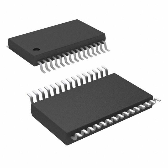
Device Information(1)
PART NUMBER
BQ78350-R1A
PACKAGE
TSSOP (30)
BODY SIZE (NOM)
7.80 mm x 6.40 mm
(1) For all available packages, see the orderable addendum at
the end of the data sheet.
Simplified Schematic
PACK+
bq76920
BAT
VC5
REGSRC
VC4
REGOUT
VC3
CAP 1
VC2
TS 1
VC1
SCL
VC0
SDA
SRP
VSS
SRN
CHG
ALERT
DSG
VCC
MRST
BAT
VAUX
KEYIN
PUSH-BUTTON
FOR BOOT
LED1
LED2
LED3
LED4
PRES
RBI
LED5
SAFE
VSS
PWRM
DISP
SCL
SDA
ALERT
COM
VEN
SMBC
SMBC
PRECHG
SMBD
GPIOA
SMBA
SMBD
GPIOB
ADREN
PACK–
Copyright © 2017, Texas Instruments Incorporated
1
An IMPORTANT NOTICE at the end of this data sheet addresses availability, warranty, changes, use in safety-critical applications,
intellectual property matters and other important disclaimers. PRODUCTION DATA.
�BQ78350-R1A
SLUSE05 – DECEMBER 2019
www.ti.com
Table of Contents
1
2
3
4
5
6
7
Features ..................................................................
Applications ...........................................................
Description .............................................................
Revision History.....................................................
Description (continued).........................................
Pin Configuration and Functions .........................
Specifications.........................................................
7.1
7.2
7.3
7.4
7.5
7.6
7.7
7.8
7.9
7.10
7.11
7.12
7.13
1
1
1
2
3
3
4
8
Detailed Description .............................................. 9
8.1
8.2
8.3
8.4
8.5
9
Overview ................................................................... 9
Functional Block Diagram ....................................... 10
Feature Description................................................. 10
Device Functional Modes........................................ 12
Programming........................................................... 12
Application and Implementation ........................ 13
9.1 Application Information............................................ 13
9.2 Typical Applications ................................................ 13
Absolute Maximum Ratings ...................................... 4
ESD Ratings.............................................................. 4
Recommended Operating Conditions....................... 4
Thermal Information .................................................. 5
Electrical Characteristics: Supply Current................. 5
Electrical Characteristics: I/O .................................... 5
Electrical Characteristics: ADC ................................. 6
Electrical Characteristics: Power-On Reset .............. 6
Electrical Characteristics: Oscillator.......................... 6
Electrical Characteristics: Data Flash Memory ....... 6
Electrical Characteristics: Register Backup ............ 7
SMBus Timing Specifications ................................. 7
Typical Characteristics ........................................... 8
10 Power Supply Recommendations ..................... 21
11 Layout................................................................... 21
11.1 Layout Guidelines ................................................. 21
11.2 Layout Example .................................................... 22
12 Device and Documentation Support ................. 23
12.1
12.2
12.3
12.4
12.5
Related Documentation.........................................
Support Resources ...............................................
Trademarks ...........................................................
Electrostatic Discharge Caution ............................
Glossary ................................................................
23
23
23
23
23
13 Mechanical, Packaging, and Orderable
Information ........................................................... 23
4 Revision History
NOTE: Page numbers for previous revisions may differ from page numbers in the current version.
2
Date
Revision
Notes
December 2019
*
Initial Release
Submit Documentation Feedback
Copyright © 2019, Texas Instruments Incorporated
Product Folder Links: BQ78350-R1A
�BQ78350-R1A
www.ti.com
SLUSE05 – DECEMBER 2019
5 Description (continued)
The BQ78350-R1A device offers optional LED or LCD display configurations for capacity reporting. It also makes
data available over its SMBus 1.1 interface. Battery history and diagnostic data is also kept within the device in
non-volatile memory and is available over the same interface.
6 Pin Configuration and Functions
30-Pin DBT Package
Pin Functions
PIN
NUMBER
PIN NAME
TYPE
1
COM
O (1)
2
ALERT
I
3
SDA
I/O
Data transfer to and from the BQ769x0 AFE. Requires a 10-k pullup to VCC
4
SCL
I/O
Communication clock to the BQ769x0 AFE. Requires a 10-k pullup to VCC
5
PRECHG
O
Programmable polarity (default is active low) output to enable an optional precharge FET. This pin
requires an external pullup to 2.5 V when configured as active high, and is open drain when
configured as active low.
6
VAUX
AI
Auxiliary voltage input. If this pin is not used, then it should be tied to VSS.
7
BAT
AI
Translated battery voltage input
8
PRES
I
Active low input to sense system insertion. This typically requires additional ESD protection. If this
pin is not used, then it should be tied to VSS.
9
KEYIN
I
A low level indicates application key-switch is inactive on position. A high level causes the DSG
protection FET to open. If this pin is not used, then it should be tied to VSS.
10
SAFE
O
Active high output to enforce an additional level of safety protection (for example, fuse blow)
11
SMBD
I/OD
12
VEN
O
13
SMBC
I/OD
SMBus clock open-drain bidirectional pin used to clock the data transfer to and from the BQ78350R1A device
14
DISP
I
Display control for the LEDs. This pin is typically connected to BQ78350-R1A device REGOUT via
a 100-KΩ resistor and a push-button switch connect to VSS. Not used with LCD display enabled
and can be tied to VSS.
15
PWRM
O
Power mode state indicator open drain output
16
LED1
O
LED1/LCD1 display segment that drives an external LED/LCD, depending on the firmware
configuration
(1)
DESCRIPTION
Open-drain output LCD common connection. Leave unconnected if not used.
Input from the BQ769x0 AFE
SMBus data open-drain bidirectional pin used to transfer an address and data to and from the
BQ78350-R1A device
Active high voltage translation enable. This open drain signal is used to switch the input voltage
divider on/off to reduce the power consumption of the BAT translation divider network.
I = Input, IA = Analog input, I/O = Input/output, I/OD = Input/Open-drain output, O = Output, OA = Analog output, P = Power
Submit Documentation Feedback
Copyright © 2019, Texas Instruments Incorporated
Product Folder Links: BQ78350-R1A
3
�BQ78350-R1A
SLUSE05 – DECEMBER 2019
www.ti.com
Pin Functions (continued)
PIN
NUMBER
PIN NAME
TYPE
17
LED2
O
LED2/LCD2 display segment that drives an external LED/LCD, depending on the firmware
configuration
18
LED3
O
LED3/LCD3 display segment that drives an external LED/LCD, depending on the firmware
configuration
19
LED4
O
LED4/LCD4 display segment that drives an external LED/LCD, depending on the firmware
configuration
20
LED5
O
LED5/LCD5 display segment that drives an external LED/LCD, depending on the firmware
configuration
21
GPIO A
I/O
Configurable Input or Output. If not used, tie to VSS.
22
VSS
—
Negative supply voltage
23
VSS
—
Negative supply voltage
24
MRST
I
25
VSS
—
Negative supply voltage
26
VCC
P
Positive supply voltage
27
RBI
P
RAM backup input. Connect a capacitor to this pin and VSS to protect loss of RAM data in case of
short circuit condition.
28
GPIO B
I/O
Configurable input or output. If not used, tie to VSS.
29
ADREN
O
Optional digital signal enables address detection measurement to reduce power consumption.
30
SMBA
IA
Optional SMBus address detection input. If this pin is not used, then it should be tied to VSS.
DESCRIPTION
Master reset input that forces the device into reset when held low. This pin must be held high for
normal operation.
7 Specifications
7.1 Absolute Maximum Ratings
Over operating free-air temperature range (unless otherwise noted) (1)
MIN
MAX
UNIT
VCC relative to VSS
Supply voltage range
–0.3
2.75
V
V(IOD) relative to VSS
Open-drain I/O pins
–0.3
6
V
VI relative to VSS
Input voltage range to all other pins
–0.3
VCC + 0.3
V
Operating free-air temperature range, TA
–40
85
°C
Storage temperature range, Tstg
–65
150
°C
(1)
Stresses beyond those listed under absolute maximum ratings may cause permanent damage to the device. These are stress ratings
only, and functional operation of the device at these or any other conditions beyond those indicated under recommended operating
conditions is not implied. Exposure to absolute–maximum–rated conditions for extended periods may affect device reliability.
7.2 ESD Ratings
VALUE
V(ESD)
(1)
(2)
Human Body Model (HBM) ESD stress voltage (1)
±2000
Charged Device Model (CDM) ESD stress voltage (2)
±500
UNIT
V
JEDEC document JEP155 states that 500-V HBM allows safe manufacturing with a standard ESD control process.
JEDEC document JEP157 states that 250-V CDM allows safe manufacturing with a standard ESD control process.
7.3 Recommended Operating Conditions
VCC = 2.4 V to 2.6 V, TA = –40°C to 85°C (unless otherwise noted)
VCC
Supply voltage
SAFE
VO
Output voltage range
NOM
MAX
2.4
2.5
2.6
UNIT
V
VCC
SMBC, SMBD, VEN
ADREN, GPIO A, GPIO B, SDATA, SCLK,
PWRM, LED1...5 (when used as GPO)
4
MIN
Submit Documentation Feedback
5.5
V
VCC
Copyright © 2019, Texas Instruments Incorporated
Product Folder Links: BQ78350-R1A
�BQ78350-R1A
www.ti.com
SLUSE05 – DECEMBER 2019
Recommended Operating Conditions (continued)
VCC = 2.4 V to 2.6 V, TA = –40°C to 85°C (unless otherwise noted)
MIN
NOM
MAX
BAT, VAUX, SMBA
VIN
Input voltage range
1
SMBD, SMBC, ALERT, DISP, PRES, KEYIN
5.5
SDATA, GPIO A, GPIO B, LED1...5 (when
used as GPI)
TOPR
UNIT
Operating Temperature
V
VCC
–40
85
°C
7.4 Thermal Information
BQ78350-R1A
THERMAL METRIC (1)
TSSOP (DBT)
UNIT
30 PINS
RθJA, High K
Junction-to-ambient thermal resistance
81.4
RθJC(top)
Junction-to-case(top) thermal resistance
16.2
RθJB
Junction-to-board thermal resistance
34.1
ψJT
Junction-to-top characterization parameter
0.4
ψJB
Junction-to-board characterization parameter
33.6
RθJC(bottom)
Junction-to-case(bottom) thermal resistance
n/a
(1)
°C/W
For more information about traditional and new thermal metrics, see the Semiconductor and IC Package Thermal Metrics application
report, SPRA953.
7.5 Electrical Characteristics: Supply Current
VCC = 2.4 V to 2.6 V, TA = –40°C to 85°C (unless otherwise noted)
PARAMETER
ICC
TEST CONDITIONS
Operating mode current
I(SLEEP)
Low-power storage mode current
SLEEP mode
I(SHUTDOWN)
Low-power SHUTDOWN mode current
SHUTDOWN mode
(1)
(2)
MIN
TYP
MAX
UNIT
650 (1)
No flash programming
300
μA
(2)
0.1
μA
1
μA
The actual current consumption of this mode fluctuates during operation over a 1-s period. The value shown is an average using the
default data flash configuration.
The actual current consumption of this mode fluctuates during operation over a user-configurable period. The value shown is an average
using the default data flash configuration.
7.6 Electrical Characteristics: I/O
VCC = 2.4 V to 2.6 V, TA = –40°C to 85°C (unless otherwise noted)
PARAMETER
TEST CONDITIONS
MIN
TYP
MAX
Output voltage low SMBC, SMBD,
SDATA, SCLK, SAFE, ADREN, VEN,
GPIO A, GPIO B, PWRM
IOL = 0.5 mA
0.4
Output voltage low LED1, LED2, LED3,
LED4, LED5
IOL = 3 mA
0.4
VOH
Output voltage high SMBC, SMBD,
SDATA, SCLK, SAFE, ADREN, VEN,
GPIO A, GPIO B, PWRM
IOH = –1 mA
VIL
Input voltage low SMBC, SMBD, SDATA,
SCLK, ALERT, DISP, SMBA, GPIO A,
GPIO B, PRES, KEYIN
VOL
VIH
UNIT
VCC – 0.5
V
V
–0.3
0.8
V
Input voltage high SMBC, SMBD,
SDATA, SCLK, ALERT, SMBA, GPIO A,
GPIO B
2
6
V
Input voltage high DISP, PRES, KEYIN
2
CIN
Input capacitance
ILKG
Input leakage current
VCC + 0.3
5
1
Submit Documentation Feedback
Copyright © 2019, Texas Instruments Incorporated
Product Folder Links: BQ78350-R1A
V
pF
µA
5
�BQ78350-R1A
SLUSE05 – DECEMBER 2019
www.ti.com
7.7 Electrical Characteristics: ADC
VCC = 2.4 V to 2.6 V, TA = –40°C to 85°C (unless otherwise noted)
PARAMETER
Input voltage range
TEST CONDITIONS
BAT, VAUX
MIN
–0.2
Conversion time
16
Resolution (no missing codes)
16
Effective resolution
13
Integral nonlinearity
±0.03%
Offset error
(2)
Offset error drift (2)
TA = 25°C to 85°C
Full-scale error (3)
Full-scale error drift
MAX
1
UNIT
V
ms
bits
14
bits
FSR (1)
140
250
µV
2.5
18
µV/°C
±0.1%
±0.7%
50
PPM/°C
8
MΩ
Effective input resistance (4)
(1)
(2)
(3)
(4)
TYP
Full-scale reference
Post-calibration performance and no I/O changes during conversion with VSS as the ground reference
Uncalibrated performance. This gain error can be eliminated with external calibration.
The A/D input is a switched-capacitor input. Since the input is switched, the effective input resistance is a measure of the average
resistance.
7.8 Electrical Characteristics: Power-On Reset
VCC = 2.4 V to 2.6 V, TA = –40°C to 85°C (unless otherwise noted)
MIN
TYP
MAX
VIT–
PARAMETER
Negative-going voltage input
TEST CONDITIONS
1.7
1.8
1.9
UNIT
V
VHYS
Power-on reset hysteresis
50
125
200
mV
MIN
TYP
MAX
UNIT
4.194
MHz
–3%
0.25%
3%
–2
0.25
2
2.5
5
7.9 Electrical Characteristics: Oscillator
VCC = 2.4 V to 2.6 V, TA = –40°C to 85°C (unless otherwise noted)
PARAMETER
f(OSC)
TEST CONDITIONS
Operating frequency
f(EIO)
Frequency error (1) (2)
t(SXO)
Start-up time (3)
TA = 20°C to 70°C
ms
LOW FREQUENCY OSCILLATOR
f(LOSC)
Operating frequency
f(LEIO)
Frequency error (2) (4)
t(LSXO)
Start-up time (5)
(1)
(2)
(3)
(4)
(5)
The
The
The
The
The
32.768
TA = 20°C to 70°C
–2.5%
0.25%
–1.5
0.25
kHz
2.5%
1.5
500
ms
frequency error is measured from 4.194 MHz.
frequency drift is included and measured from the trimmed frequency at VCC = 2.5 V, TA = 25°C.
start-up time is defined as the time it takes for the oscillator output frequency to be within 1% of the specified frequency.
frequency error is measured from 32.768 kHz.
start-up time is defined as the time it takes for the oscillator output frequency to be ±3%.
7.10 Electrical Characteristics: Data Flash Memory
VCC = 2.4 V to 2.6 V, TA = –40°C to 85°C (unless otherwise noted)
PARAMETER
tDR
TEST CONDITIONS
MAX
UNIT
10
Years
Flash programming write-cycles
See note (1)
20,000
Cycles
(1)
Word programming time
See note
I(DDdPROG)
Flash-write supply current
See note (1)
6
TYP
See note (1)
t(WORDPROG)
(1)
MIN
Data retention
5
2
ms
10
mA
Specified by design. Not production tested
Submit Documentation Feedback
Copyright © 2019, Texas Instruments Incorporated
Product Folder Links: BQ78350-R1A
�BQ78350-R1A
www.ti.com
SLUSE05 – DECEMBER 2019
7.11 Electrical Characteristics: Register Backup
VCC = 2.4 V to 2.6 V, TA = –40°C to 85°C (unless otherwise noted)
PARAMETER
I(RB)
RB data-retention input
current
V(RB)
RB data-retention
voltage (1)
(1)
TEST CONDITIONS
MIN
TYP
V(RB) > V(RBMIN), VCC < VIT–
V(RB) > V(RBMIN), VCC < VIT–, TA = 0°C
to 50°C
40
MAX
UNIT
1500
nA
160
1.7
V
Specified by design. Not production tested
7.12 SMBus Timing Specifications
VCC = 2.4 V to 2.6 V, TA = –40°C to 85°C (unless otherwise noted)
PARAMETER
TEST CONDITIONS
MIN
NOM
MAX
UNIT
100
kHz
fSMB
SMBus operating
frequency
SLAVE mode, SMBC 50% duty cycle
fMAS
SMBus master clock
frequency
MASTER mode, no clock low slave
extend
tBUF
Bus free time between
start and stop
tHD:STA
Hold time after
(repeated) start
tSU:STA
Repeated start setup
time
tSU:STO
Stop setup time
tHD:DAT
Data hold time
tSU:DAT
Data setup time
tTIMEOUT
Error signal/detect
tLOW
Clock low period
tHIGH
Clock high period
See note (2)
tLOW:SEXT
Cumulative clock low
slave extend time
See note (3)
25
tLOW:MEXT
Cumulative clock low
master extend time
See note (4)
10
tF
Clock/data fall time
(VILMAX – 0.15 V) to (VIHMIN + 0.15 V)
tR
Clock/data rise time
0.9 VCC to (VILMAX – 0.15 V)
(1)
(2)
(3)
(4)
RECEIVE mode
TRANSMIT mode
10
51.2
kHz
4.7
µs
4
µs
4.7
µs
4
µs
0
300
ns
250
See note (1)
25
35
4.7
4
ms
µs
50
300
ms
ns
1000
The BQ78350-R1A device times out when any clock low exceeds tTIMEOUT.
tHIGH:MAX is minimum bus idle time. SMBC = 1 for t > 50 μs causes a reset of any transaction in progress involving the BQ78350-R1A
device.
tLOW:SEXT is the cumulative time a slave device is allowed to extend the clock cycles in one message from initial start to stop.
tLOW:MEXT is the cumulative time a master device is allowed to extend the clock cycles in one message from initial start to stop.
Submit Documentation Feedback
Copyright © 2019, Texas Instruments Incorporated
Product Folder Links: BQ78350-R1A
7
�BQ78350-R1A
SLUSE05 – DECEMBER 2019
www.ti.com
Figure 1. SMBus Timing Diagram
7.13 Typical Characteristics
174.5
1.2275
174.0
1.2270
ADC Offset Error ( V)
Internal Voltage Reference (V)
1.2280
1.2265
1.2260
1.2255
1.2250
1.2245
1.2240
173.5
173.0
172.5
172.0
171.5
1.2235
1.2230
171.0
±40
±20
0
20
40
60
Temperature (ƒC)
80
±40
C001
Figure 2. Internal Voltage Reference
8
Submit Documentation Feedback
±20
0
20
40
Temperature (ƒC)
60
80
C002
Figure 3. ADC Offset Error
Copyright © 2019, Texas Instruments Incorporated
Product Folder Links: BQ78350-R1A
�BQ78350-R1A
www.ti.com
SLUSE05 – DECEMBER 2019
Typical Characteristics (continued)
3.05
32.85
32.80
2.95
LFO Frequency (kHz)
LED Sink Current (mA)
3.00
2.90
2.85
2.80
2.75
2.70
2.65
32.75
32.70
32.65
32.60
2.60
2.55
32.55
±40
±20
0
20
40
60
Temperature (ƒC)
80
±40
0
±20
20
40
60
80
Temperature (ƒC)
C003
Figure 4. LED Sink Current
C004
Figure 5. LFO Frequency
4.190
HFO Frequency (MHz)
4.185
4.180
4.175
4.170
4.165
4.160
±40
±20
0
20
40
Temperature (ƒC)
60
80
C005
Figure 6. HFO Frequency
8 Detailed Description
8.1 Overview
The BQ78350-R1A li-ion and LiFePO4 Battery Management Controller is the companion to the BQ769x0 family
of Analog Front End (AFE) protection devices. This chipset supports 3-series to 15-series cell applications with
capacities up to 320 Ah, and is suitable for a wide range of portable or stationary battery applications. The
BQ78350-R1A device provides an accurate fuel gauge and state-of-health (SoH) monitor, as well as the cell
balancing algorithm and a full range of voltage-, current-, and temperature-based protection features.
The battery data that the BQ78350-R1A device gathers can be accessed via an SMBus 1.1 interface, and stateof-charge (SoC) data can be displayed through optional LED or LCD display configurations. Battery history and
diagnostic data are also kept within the device in non-volatile memory and are available over the same SMBus
interface.
Submit Documentation Feedback
Copyright © 2019, Texas Instruments Incorporated
Product Folder Links: BQ78350-R1A
9
�BQ78350-R1A
SLUSE05 – DECEMBER 2019
www.ti.com
8.2 Functional Block Diagram
COM, ALERT,
KEYIN, SAFE,
SMBD, SMBC,
VEN, DISP
SMBA, ADREN,
SDA, SCL,
PRECHG,VAUX,
BAT, PRES
GPIOA
GPIOB
LED1...5
PWRM
8
8
8
Oscillator
System Clock
32 kHz
Interrupt *
2
Input/Output
Event*
1
Power
Regulation
AND
Management
Interrupt
Controller
VCC
V SS
MRST
RBI
System Clocks
Reset*
Wake Comparator
Event*
Analog Front End
Delta-Sigma ADC
AND
Integrating
Coulomb Counter
Data (8-bit)
CoolRISC
CPU
DMAddr (16-bit)
SRP
SRN
System I /O (13-bit)
PMAddr
(15-bit)
PMInst
(22-bit)
Program Memory
Data Memory
Communications
SMBus
Peripherals
and
Timers
Copyright © 2017, Texas Instruments Incorporated
8.3 Feature Description
The following section provides an overview of the device features. For full details on the BQ78350-R1A features,
refer to the BQ78350-R1A Technical Reference Manual (SLUUBD3).
8.3.1 Primary (1st Level) Safety Features
The BQ78350-R1A device supports a wide range of battery and system protection features that can be
configured. The primary safety features include:
• Cell over/undervoltage protection
• Charge and discharge overcurrent
• Short circuit protection
• Charge and discharge overtemperature with independent alarms and thresholds for each thermistor
8.3.2 Secondary (2nd Level) Safety Features
The secondary safety features of the BQ78350-R1A device can be used to indicate more serious faults via the
SAFE pin. This pin can be used to blow an in-line fuse to permanently disable the battery pack from charging or
discharging. The secondary safety protection features include:
• Safety overvoltage
• Safety undervoltage
• Safety overcurrent in charge and discharge
• Safety overtemperature in charge and discharge
• Charge FET and Precharge FET fault
10
Submit Documentation Feedback
Copyright © 2019, Texas Instruments Incorporated
Product Folder Links: BQ78350-R1A
�BQ78350-R1A
www.ti.com
SLUSE05 – DECEMBER 2019
Feature Description (continued)
•
•
•
•
Discharge FET fault
Cell imbalance detection
Open thermistor detection
AFE communication fault
8.3.3 Charge Control Features
The BQ78350-R1A charge control features include:
• Provides a range of options to configure the charging algorithm and its actions based on the application
requirements
• Reports the appropriate charging current needed for constant current charging, and the appropriate charging
voltage needed for constant voltage charging
• Supports pre-charging/0-volt charging
• Supports charge inhibit and charge suspend if battery pack temperature is out of temperature range
8.3.4 Fuel Gauging
The BQ78350-R1A device uses Compensated End-of-Discharge Voltage (CEDV) technology to measure and
calculate the available charge in battery cells. The BQ78350-R1A device accumulates a measure of charge and
discharge currents and compensates the charge current measurement for the temperature and state-of-charge of
the battery. The BQ78350-R1A device estimates self-discharge of the battery and also adjusts the self-discharge
estimation based on temperature.
8.3.5 Lifetime Data Logging
The BQ78350-R1A device offers lifetime data logging, where important measurements are stored for warranty
and analysis purposes. The data monitored includes:
• Lifetime maximum temperature
• Lifetime minimum temperature
• Lifetime maximum battery cell voltage per cell
• Lifetime minimum battery cell voltage per cell
• Cycle count
• Maximum charge current
• Maximum discharge current
• Safety events that trigger SafetyStatus() updates. (The 12 most common are tracked.)
8.3.6 Authentication
The BQ78350-R1A device supports authentication by the host using SHA-1.
8.3.7 Battery Parameter Measurements
The BQ78350-R1A device digitally reads BQ769x0 registers containing recent values from the integrating
analog-to-digital converter (CC) for current measurement and a second delta-sigma ADC for individual cell and
temperature measurements.
8.3.7.1 Current and Coulomb Counting
The integrating delta-sigma ADC (CC) in the companion BQ769x0 AFE measures the charge/discharge flow of
the battery by measuring the voltage drop across a small-value sense resistor between the SRP and SRN pins.
The 15-bit integrating ADC measures bipolar signals from –0.20 V to 0.20 V with 15-µV resolution. The AFE
reports charge activity when VSR = V(SRP) – V(SRN) is positive, and discharge activity when VSR = V(SRP) – V(SRN)
is negative. The BQ78350-R1A device continuously monitors the measured current and integrates the digital
signal from the AFE over time, using an internal counter.
To support large battery configurations, the current data can be scaled to ensure accurate reporting through the
SMBus. The data reported is scaled based on the setting of the SpecificationInfo() command.
Submit Documentation Feedback
Copyright © 2019, Texas Instruments Incorporated
Product Folder Links: BQ78350-R1A
11
�BQ78350-R1A
SLUSE05 – DECEMBER 2019
www.ti.com
Feature Description (continued)
8.3.7.2 Voltage
The BQ78350-R1A device updates the individual series cell voltages through the BQ769x0 at 1-s intervals. The
BQ78350-R1A device configures the BQ769x0 to connect to the selected cells in sequence and uses this
information for cell balancing and individual cell fault functions. The internal 14-bit ADC of the BQ769x0
measures each cell voltage value, which is then communicated digitally to the BQ78350-R1A device where they
are scaled and translated into unit mV. The maximum supported input range of the ADC is 6.075 V.
The BQ78350-R1A device also separately measures the average cell voltage through an external translation
circuit at the BAT pin. This value is specifically used for the fuel gauge algorithm. The external translation circuit
is controlled via the VEN pin so that the translation circuit is only enabled when required to reduce overall power
consumption. For correct operation, VEN requires an external pull-up to VCC, typically 100 k.
In addition to the voltage measurements used by the BQ78350-R1A algorithms, there is an optional auxiliary
voltage measurement capability via the VAUX pin. This feature measures the input on a 1-s update rate and
provides the programmable scaled value through an SMBus command.
To support large battery configurations, the voltage data can be scaled to ensure accurate reporting through the
SMBus. The data reported is scaled based on the setting of the SpecificationInfo() command.
8.3.7.3 Temperature
The BQ78350-R1A device receives temperature information from external or internal temperature sensors in the
BQ769x0 AFE. Depending on the number of series cells supported, the AFE will provide one, two, or three
external thermistor measurements.
8.4 Device Functional Modes
The BQ78350-R1A device supports three power modes to optimize the power consumption:
• In NORMAL mode, the device performs measurements, calculations, protection decisions, and data updates
in 1-s intervals. Between these intervals, the device is in a reduced power mode.
• In SLEEP mode, the device performs measurements, calculations, protection decisions, and data updates in
adjustable time intervals. Between these intervals, the device is in a reduced power mode.
• In SHUTDOWN mode, the device is completely powered down.
The device indicates through the PWRM pin which power mode it is in. This enables other circuits to change
based on the power mode detection criteria of the device.
8.5 Programming
8.5.1 Physical Interface
The device uses SMBus 1.1 with packet error checking (PEC) as an option and is used as a slave only.
8.5.2 SMBus Address
The device determines its SMBus 1.1 slave address through a voltage on SMBA, Pin 30. The voltage is set with
a pair of high-value resistors if an alternate address is required and is measured either upon exit of POR or when
system present is detected. ADREN, Pin 29, may be used to disable the voltage divider after use to reduce
power consumption.
8.5.3 SMBus On and Off State
The device detects an SMBus off state when SMBC and SMBD are logic-low for ≥ 2 seconds. Clearing this state
requires either SMBC or SMBD to transition high. Within 1 ms, the communication bus is available.
12
Submit Documentation Feedback
Copyright © 2019, Texas Instruments Incorporated
Product Folder Links: BQ78350-R1A
�BQ78350-R1A
www.ti.com
SLUSE05 – DECEMBER 2019
9 Application and Implementation
9.1 Application Information
The BQ78350-R1A Battery Management Controller companion to the BQ769x0 family of battery monitoring AFEs
enables many standard and enhanced battery management features in a 3-series to 15-series li-ion/li-polymer
battery pack.
To design and implement a complete solution, users need the Battery Management Studio (BQSTUDIO) tool to
configure a "golden image" set of parameters for a specific battery pack and application. The BQSTUDIO tool is
a graphical user-interface tool installed on a PC during development. The firmware installed in the product has
default values, which are summarized in the BQ78350-R1A Technical Reference Manual (SLUUBD3). With the
BQSTUDIO tool, users can change these default values to cater to specific application requirements. Once the
system parameters are known (for example, fault trigger thresholds for protection, enable/disable of certain
features for operation, configuration of cells, among others), the data can be saved. This data is referred to as
the "golden image.”
9.2 Typical Applications
The BQ78350-R1A device can be used with the BQ76920, BQ76930, or BQ76940 device, but it is set up, by
default, for a 5-series cell, 4400-mA battery application using the BQ76920 AFE.
Submit Documentation Feedback
Copyright © 2019, Texas Instruments Incorporated
Product Folder Links: BQ78350-R1A
13
�14
Submit Documentation Feedback
Product Folder Links: BQ78350-R1A
J4
BATT-
SMB is required for
gauge setup.
Signals would require isolation
circuit for use in system
SMB
1
2
3
4
GND
E2
E4
D32
5.6V
D30
5.6V
GND
R73
R76
1.00Meg 1.00Meg
100
100 R80
100
R72
R77
ALERT
SDA
SCL
REGOUT
BATT+
100
R70
GND
R48
13.7k
C23
3300pF
R47
300k
25 ppm/C
Q8
BSS84-7-F
GND
R50
100k
R49
100k
CSD17381F4
Q9
R51
1.00Meg
GND
1
28
30
24
11
13
8
9
2
3
4
6
7
26
BQ78350DBT
NC
NC
SMBA
MRST
SMBD
SMBC
PRES
KEYIN
ALERT
SDA
SCL
VAUX
BAT
VCC
U2
VSS
VSS
VSS
VSS
RBI
PRECHG
PWRM
SAFE
ADREN
VEN
DISP
LED1
LED2
LED3
LED4
LED5
21
22
23
25
27
5
15
10
29
12
14
16
17
18
19
20
GND
GND
C25
0.1µF
R57
221k
Copyright © 2017, Texas Instruments Incorporated
GND
C24
0.1µF
R55
100k
PRE
BQ78350-R1A
SLUSE05 – DECEMBER 2019
www.ti.com
Typical Applications (continued)
9.2.1 Schematic
The schematic is split into two sections: the gas gauge section (Figure 7) and the AFE section (Figure 8).
Figure 7. 5-Series Cell Typical Schematic, Gas Gauge (BQ78350-R1A)
Copyright © 2019, Texas Instruments Incorporated
�395021006
1
2
3
4
5
6
C5
C4
C3
C2
C1
C0
BATT-
C0
C1
C2
C3
C4
C5
R11
10.0k
R12
100
R13
100
R15
100
R16
100
R17
100
R18
100
R19
100
Copyright © 2019, Texas Instruments Incorporated
Product Folder Links: BQ78350-R1A
BATT-
GND
BATT+
D23
SMCJ28A
28V
GND
C1
1µF
C3
1µF
C4
1µF
C5
1µF
C6
1µF
C7
1µF
GND
GND
Net-Tie
NT1
0.1µF
C27
0.001
R60
R59
100
0.1µF
C28
R61
100
GND
GND
0.1µF
C29
R35
499k
C13
470pF
11
20
19
18
12
13
14
15
16
17
C1
R36
Q12
CSD17501Q5A
5,6,
7,8
R63
0
PRE
VSS
CHG
DSG
SCL
SDA
TS1
CAP1
REGOUT
3.01k
1,2,3
R62
1.00Meg
ALERT
BAT
REGSRC
BQ7692000PW
NC
ALERT
SRN
SRP
VC5
VC4
VC3
VC2
VC1
VC0
U1
10
1
2
C31
0.1µF
0.1µF
1.0k
R64
10.0k
R65
4-1437565-1
S1
GND
C15
2.2µF
C30
3
4
GND
3
2
1
5
4
6
7
8
9
3
1
2
R67
1.00Meg
Q13
CSD17381F4
R66
10.0k
D24
Q14
MMBTA92
C16
1µF
GND
10V
D25
18V
D26
C18
4700pF
t°
1,2,3
R68
1.00Meg
R69
1.00k
Q16
Q15
CSD17501Q5A
5,6,
7,8
CHG
GND
RT1
10.0k ohm
4
D11
4
J1
BATT+
R71
1.00Meg
D27
16V
D28
C21
4.7µF
D29
R41
R42
10.0k 10.0k
C32
0.1µF
C33
0.1µF
E1
SCL
SDA
PACK+
PACK-
REGOUT
J3
1
J2
1
www.ti.com
SLUSE05 – DECEMBER 2019
BQ78350-R1A
Typical Applications (continued)
Figure 8. 5-Series Cell Typical Schematic, AFE (BQ76920)
Submit Documentation Feedback
15
�BQ78350-R1A
SLUSE05 – DECEMBER 2019
www.ti.com
Typical Applications (continued)
9.2.2 Design Requirements
Table 1 lists the device's default settings and feature configurations when shipped from Texas Instruments.
Table 1. TI Default Settings
Design Parameter
Value or State
Cell Configuration
5s2p (5-series with 1 Parallel)
Design Capacity
4400 mAh
Device Chemistry
Chem ID 1210 (LiCoO2/graphitized carbon)
Cell Over Voltage (per cell)
4250 mV
Cell Under Voltage (per cell)
2500 mV
Overcurrent in CHARGE Mode
6000 mA
Overcurrent in DISCHARGE Mode
–6000 mA
Over Load Current
0.017 V/Rsense across SRP, SRN
Short Circuit in DISCHARGE Mode
0.44 V/Rsense across SRP, SRN
Over Temperature in CHARGE Mode
55°C
Over Temperature in DISCHARGE Mode
55°C
SAFE Pin Activation Enabled
No
Safety Overvoltage (per cell)
4400 mV
Safety Undervoltage (per cell)
2500 mV
Shutdown Voltage
2300 mV
Cell Balancing Enabled
Yes
Internal or External Temperature Sensor
External Enabled
SMB BROADCAST Mode
Disabled
Display Mode (# of bars and LED or LCD)
5-bar LED
Dynamic SMB Address Enabled
No (SMB Address = 0x16)
KEYIN Feature Enabled
No
PRES Feature Enabled
No
9.2.3 Detailed Design Procedure
By default, the BQ78350-R1A device is initially set up to keep the CHG, DSG, and PCHG FETs OFF and many
other features disabled until the appropriate ManufacturingStatus() bit that enables ManufacturerAccess()
commands are received, or when the default Manufacturing Status is changed.
In the first steps to evaluating the device and BQ769x0 AFE, use the ManufacturerAccess() commands to ensure
correct operation of features, and if they are needed in the application. Then enable features' reading for more indepth application evaluation.
Prior to using the device, the default settings should be evaluated as the device has many configuration settings
and options. These can be separated into five main areas:
• Measurement System
• Gas Gauging
• Charging
• Protection
• Peripheral Features
The key areas of focus are covered in the following sections.
16
Submit Documentation Feedback
Copyright © 2019, Texas Instruments Incorporated
Product Folder Links: BQ78350-R1A
�BQ78350-R1A
www.ti.com
SLUSE05 – DECEMBER 2019
9.2.3.1 Measurement System
9.2.3.1.1 Cell Voltages
The device is required to be configured in the AFE Cell Map register to determine which cells to measure based
on the physical connections to the BQ76920 AFE. The cell voltage data is available through
CellVoltage1()…CellVoltage5(). The cell voltages are reported as they are physically stacked. For example, if the
device is configured for 3-series cells connected to VC1, VC2, and VC5 per the AFE Cell Map, then the cell
voltages are still reported via CellVoltage1(), CellVoltage2(), and CellVoltage3(), respectively.
For improved accuracy, offset calibration is available for each of these values and can be managed through the
BQSTUDIO tool. The procedure for calibration is described in the BQ78350-R1A Technical Reference Manual
(SLUUBD3) in the Calibration chapter.
9.2.3.1.2 External Average Cell Voltage
This is enabled by default (DA Configuration [ExtAveEN] = 1) and uses the external resistor divider connected
to the VEN and BAT pins to determine the average cell voltage of the battery pack. The average cell voltage is
available through ExtAveCellVoltage().
CAUTION
Care should be taken in the selection of the resistor and FETs used in this divider
circuit as the tolerance and temperature drift of these components can cause
increased measurement error and a gas gauging error if CEDV Gauging Config
[ExtAveCell] = 1 (default = 1).
For improved accuracy, offset and gain calibration is available for this value and can be managed through the
BQSTUDIO tool. The procedure for calibration is described in the BQ78350-R1A Technical Reference Manual
(SLUUBD3) in the Calibration chapter.
9.2.3.1.3 Current
Current data is taken from the BQ76920 and made available through Current(). The selection of the current
sense resistor connected to SRP and SRN of the BQ76920 is very important and there are several factors
involved.
The aim of the sense resistor selection is to use the widest ADC input voltage range possible.
To maximize accuracy, the sense resistor value should be calculated based on the following formula:
RSNS(min) = V(SRP) – V(SRN) / I(max)
Where: |V(SRP) – V(SRN)| = 200 mV
I(max) = Maximum magnitude of charge of discharge current (transient or DC)
(1)
NOTE
RSNS(min) should include tolerance, temperature drift over the application temperature,
and PCB layout tolerances when selecting the actual nominal resistor value.
When selecting the RSNS value, be aware that when selecting a small value, for example,
1 mΩ, then the resolution of the current measurement will be > 1 mA. In the example of
RSNS = 1 mΩ, the current LSB will be 8.44 mA.
For improved accuracy, offset and gain calibration are available for this value and can be managed through the
BQSTUDIO tool. The procedure for calibration is described in the BQ78350-R1A Technical Reference Manual
(SLUUBD3) in the Calibration chapter.
Submit Documentation Feedback
Copyright © 2019, Texas Instruments Incorporated
Product Folder Links: BQ78350-R1A
17
�BQ78350-R1A
SLUSE05 – DECEMBER 2019
www.ti.com
9.2.3.1.4 Temperature
By default, the 78350 uses an external negative temperature coefficient (NTC) thermistor connected to the
BQ76920 as the source for the Temperature() data. The measurement uses a polynomial expression to
transform the BQ76920 ADC measurement into 0.1°C resolution temperature measurement. The default
polynomial coefficients are calculated using the Semitec 103AT, although other resistances and manufacturers
can be used.
To calculate the External Temp Model coefficients, use the BQ78350-R1 Family Thermistor Coefficient
Calculator shown in the application report, Using the BQ78350-R1 (SLUA924).
For improved accuracy, offset calibration is available for this value and can be managed through the BQSTUDIO
tool. The procedure for calibration is described in the BQ78350-R1A Technical Reference Manual (SLUUBD3) in
the Calibration chapter.
9.2.3.2 Gas Gauging
The default battery chemistry (Chem ID) is 1210, which is a Li-CoO2 type chemistry. The Chem ID should be
updated using BQSTUDIO to select the specific battery used in the application. See the application report, Using
the BQ78350-R1 (SLUA924) for details on selecting the Chem ID.
The default maximum capacity of the battery is 4400 mAh and this should be changed based on the cell and
battery configuration chosen.
The CEDV gas gauging algorithm requires seven coefficients to enable accurate gas gauging. The default values
are generic for Li-CoO2 chemistry, but for accurate gas gauging these coefficients should be re-calculated. The
procedure to gather the required data and generate the coefficients can be found at
http://www.ti.com/tool/GPCCEDV.
More details on the required steps to set up the BQ78350-R1A device for gas gauging can be found in the
application report, Using the BQ78350-R1 (SLUA924).
9.2.3.3 Charging
The charging algorithm in the BQ78350-R1A device is configured to support Constant Voltage/Constant Current
(CC/CV) charging of a nominal 18-V, 4400-mAh battery.
9.2.3.3.1 Fast Charging Voltage
The charging voltage is configured (Fast Charging: Voltage) based on an individual cell basis (for example, 4200
mV), but the ChargingVoltage() is reported as the required battery voltage (for example, 4200 mV × 5 =
21000 mV).
9.2.3.3.2 Fast Charging Current
The fast charging current is configured to 2000 mA (Fast Charging: Current) by default, which is conservative for
the majority of 4400-mAh battery applications. This should be configured based on the battery configuration, cell
manufacturer's data sheet, and system power design requirements.
9.2.3.3.3 Other Charging Modes
The BQ78350-R1A device is configured to limit, through external components, and report either low or 0
ChargingVoltage() and ChargingCurrent(), based on temperature, voltage, and fault status information.
The Charge Algorithm section of the BQ78350-R1A Technical Reference Manual (SLUUBD3) details these
features and settings.
9.2.3.4 Protection
The safety features and settings of the BQ78350-R1A device are configured conservatively and are suitable for
bench evaluation. However, in many cases, users will need to change these values to meet system
requirements. These values should not be changed to exceed the safe operating limits provided by the cell
manufacturer and any industry standard.
For details on the safety features and settings, see the Protections and Permanent Fail sections of the
BQ78350-R1A Technical Reference Manual (SLUUBD3).
18
Submit Documentation Feedback
Copyright © 2019, Texas Instruments Incorporated
Product Folder Links: BQ78350-R1A
�BQ78350-R1A
www.ti.com
SLUSE05 – DECEMBER 2019
9.2.3.5 Peripheral Features
9.2.3.5.1 LED Display
The BQ78350-R1A device is configured by default to display up to five LEDs in a bar graph configuration based
on the value of RemainingStateOfCharge() (RSOC). Each LED represents 20% of RSOC and is illuminated
when the BQ78350-R1A DISP pin transitions low, and remains on for a programmable period of time.
In addition to many other options, the number of LEDs used and the percentage at which they can be illuminated
are configurable.
9.2.3.5.2 SMBus Address
Although the SMBus slave address is a configurable value in the BQ78350-R1A device, this feature is disabled
by default and the slave address is 0x16. The SMBus Address feature can allow up to nine different addresses
based on external resistor value variation per address.
The default setup of the BQ78350-R1A device is generic, but there are many additional features that can be
enabled and configured to support a variety of system requirements. These are detailed in the BQ78350-R1A
Technical Reference Manual (SLUUBD3).
9.2.4 Application Performance Plots
When the BQ78350-R1A device is powered up, there are several signals that are enabled at the same time.
Figure 9 shows the rise time of each of the applicable signals.
Figure 9. VCC, MRST, VEN, and PWRM upon Power Up
Submit Documentation Feedback
Copyright © 2019, Texas Instruments Incorporated
Product Folder Links: BQ78350-R1A
19
�BQ78350-R1A
SLUSE05 – DECEMBER 2019
www.ti.com
The BQ78350-R1A device takes a short period of time to boot up before the device can begin updating battery
parameter data that can be then reported via the SMBus or the optional display. Normal operation after boot-up
is indicated by the VEN pin pulsing to enable voltage data measurements for the ExtAveCell() function. Figure 10
shows the timing of these signals.
Figure 10. Valid VCC to Full FW Operation
Figure 11, Figure 12, Figure 13, and Figure 14 show Measurement System Performance Data of the BQ78350R1A device + the BQ76920 EVM. This data was taken using a standard BQ76920 EVM with power supplies
providing the voltage and current reference inputs.
10
8
10
At 4200mV
8
6
4
Current Error (mA)
Voltage Error (mV)
6
2
0
±2
±4
±6
4
2
0
±2
±4
±6
±8
±8
±10
±10
±40
±20
0
20
40
60
80
100
Forced Temperature (ƒC)
±20
0
20
40
Forced Temperature (ƒC)
C006
Figure 11. Cell Voltage Error Reported Through
CellVoltage1…5()
20
At 2000mA
60
80
C008
Figure 12. Battery Charge Current Error Reported Through
Current()
Submit Documentation Feedback
Copyright © 2019, Texas Instruments Incorporated
Product Folder Links: BQ78350-R1A
�BQ78350-R1A
www.ti.com
SLUSE05 – DECEMBER 2019
6
10
8
At ±2000mA
4
Temperature Error (ƒC)
Current Error (mA)
6
4
2
0
±2
±4
±6
2
0
±2
±4
±6
±8
±10
±12
±8
±10
±14
±20
0
20
40
60
Forced Temperature (ƒC)
80
±20
Figure 13. Battery Discharge Current Error Reported
Through Current()
0
20
40
60
80
Forced Temperature (ƒC)
C009
C007
Figure 14. Battery Temperature (External) Error Reported
Through Temperature()
10 Power Supply Recommendations
The BQ78350-R1A device is powered directly from the 2.5-V REGOUT pin of the BQ769x0 companion AFE. An
input capacitor of 0.1 µF is required between VCC and VSS and should be placed as close to the BQ78350-R1A
device as possible.
To ensure correct power up of the BQ78350-R1A device, a 100-k resistor between MRST and VCC is also
required. See the Schematic for further details.
11 Layout
11.1 Layout Guidelines
11.1.1 Power Supply Decoupling Capacitor
Power supply decoupling from VCC to ground is important for optimal operation of the BQ78350-R1A device. To
keep the loop area small, place this capacitor next to the IC and use the shortest possible traces. A large-loop
area renders the capacitor useless and forms a small-loop antenna for noise pickup.
Ideally, the traces on each side of the capacitor must be the same length and run in the same direction to avoid
differential noise during ESD. If possible, place a via near the VSS pin to a ground plane layer.
Placement of the RBI capacitor is not as critical. It can be placed further away from the IC.
11.1.2 MRST Connection
The MRST pin controls the gas gauge reset state. The connections to this pin must be as short as possible to
avoid any incoming noise. Direct connection to VCC is possible if the reset functionality is not desired or
necessary.
If unwanted resets are found, one or more of the following solutions may be effective:
• Add a 0.1-μF capacitor between MRST and ground.
• Provide a 1-kΩ pullup resistor to VCC at MRST.
• Surround the entire circuit with a ground pattern.
If a test point is added at MRST, it must be provided with a 10-kΩ series resistor.
11.1.3 Communication Line Protection Components
The 5.6-V Zener diodes, which protect the BQ78350-R1A communication pins from ESD, must be located as
close as possible to the pack connector. The grounded end of these Zener diodes must be returned to the
PACK(–) node, rather than to the low-current digital ground system. This way, ESD is diverted away from the
sensitive electronics as much as possible.
Submit Documentation Feedback
Copyright © 2019, Texas Instruments Incorporated
Product Folder Links: BQ78350-R1A
21
�BQ78350-R1A
SLUSE05 – DECEMBER 2019
www.ti.com
Layout Guidelines (continued)
11.1.4 ESD Spark Gap
Protect the SMBus clock, data, and other communication lines from ESD with a spark gap at the connector. The
following pattern is recommended, with 0.2-mm spacing between the points.
Figure 15. Recommended Spark-Gap Pattern Helps Protect Communication Lines From ESD
11.2 Layout Example
C21
C22
bq78350
VCC
RBI
Figure 16. BQ78350-R1A Layout
22
Submit Documentation Feedback
Copyright © 2019, Texas Instruments Incorporated
Product Folder Links: BQ78350-R1A
�BQ78350-R1A
www.ti.com
SLUSE05 – DECEMBER 2019
12 Device and Documentation Support
12.1 Related Documentation
For related documentation, see the following:
• BQ78350-R1A Technical Reference Manual (SLUUC78)
• Using the BQ78350-R1 Application Report (SLUA924)
• BQ769x0 3-Series to 15-Series Cell Battery Monitor Family for Li-Ion and Phosphate Applications Data
Manual (SLUSBK2)
12.2 Support Resources
TI E2E™ support forums are an engineer's go-to source for fast, verified answers and design help — straight
from the experts. Search existing answers or ask your own question to get the quick design help you need.
Linked content is provided "AS IS" by the respective contributors. They do not constitute TI specifications and do
not necessarily reflect TI's views; see TI's Terms of Use.
12.3 Trademarks
E2E is a trademark of Texas Instruments.
All other trademarks are the property of their respective owners.
12.4 Electrostatic Discharge Caution
This integrated circuit can be damaged by ESD. Texas Instruments recommends that all integrated circuits be handled with
appropriate precautions. Failure to observe proper handling and installation procedures can cause damage.
ESD damage can range from subtle performance degradation to complete device failure. Precision integrated circuits may be more
susceptible to damage because very small parametric changes could cause the device not to meet its published specifications.
12.5 Glossary
SLYZ022 — TI Glossary.
This glossary lists and explains terms, acronyms, and definitions.
13 Mechanical, Packaging, and Orderable Information
The following pages include mechanical, packaging, and orderable information. This information is the most
current data available for the designated devices. This data is subject to change without notice and revision of
this document. For browser-based versions of this data sheet, refer to the left-hand navigation.
Submit Documentation Feedback
Copyright © 2019, Texas Instruments Incorporated
Product Folder Links: BQ78350-R1A
23
�PACKAGE OPTION ADDENDUM
www.ti.com
10-Dec-2020
PACKAGING INFORMATION
Orderable Device
Status
(1)
Package Type Package Pins Package
Drawing
Qty
Eco Plan
(2)
Lead finish/
Ball material
MSL Peak Temp
Op Temp (°C)
Device Marking
(3)
(4/5)
(6)
BQ78350DBT-R1A
ACTIVE
TSSOP
DBT
30
60
RoHS & Green
NIPDAU
Level-2-260C-1 YEAR
-40 to 85
78350R1A
BQ78350DBTR-R1A
ACTIVE
TSSOP
DBT
30
2000
RoHS & Green
NIPDAU
Level-2-260C-1 YEAR
-40 to 85
78350R1A
(1)
The marketing status values are defined as follows:
ACTIVE: Product device recommended for new designs.
LIFEBUY: TI has announced that the device will be discontinued, and a lifetime-buy period is in effect.
NRND: Not recommended for new designs. Device is in production to support existing customers, but TI does not recommend using this part in a new design.
PREVIEW: Device has been announced but is not in production. Samples may or may not be available.
OBSOLETE: TI has discontinued the production of the device.
(2)
RoHS: TI defines "RoHS" to mean semiconductor products that are compliant with the current EU RoHS requirements for all 10 RoHS substances, including the requirement that RoHS substance
do not exceed 0.1% by weight in homogeneous materials. Where designed to be soldered at high temperatures, "RoHS" products are suitable for use in specified lead-free processes. TI may
reference these types of products as "Pb-Free".
RoHS Exempt: TI defines "RoHS Exempt" to mean products that contain lead but are compliant with EU RoHS pursuant to a specific EU RoHS exemption.
Green: TI defines "Green" to mean the content of Chlorine (Cl) and Bromine (Br) based flame retardants meet JS709B low halogen requirements of