Product
Folder
Order
Now
Support &
Community
Tools &
Software
Technical
Documents
BQ79606A-Q1
SLUSDQ4 – APRIL 2019
BQ79606A-Q1 SafeTI™ Precision Monitor With Integrated Hardware Protector for
Automotive Battery Pack Applications
1 Features
2 Applications
•
•
•
•
•
•
•
•
•
•
•
•
•
•
•
•
The BQ79606A-Q1 includes an auxiliary ADC that
supports cell temperature measurements for up to six
NTCs as well as internal rails to enable safety checks
for the device. A die temperature measurement ADC
is also included to provide temperature correction to
enable high accuracy results over an extended
temperature range.
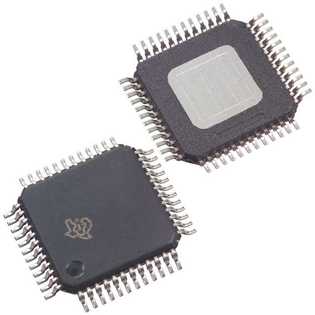
Device Information(1)
PART NUMBER
BQ79606A-Q1
PACKAGE
BODY SIZE (NOM)
PQFP (48 pin)
7.00 mm × 7.00 mm
(1) For all available packages, see the orderable addendum at
the end of the data sheet.
Simplified System Diagram
CAN Interface
Module
Connector
+
+
+
+
+
+
+
+
+
+
•
•
•
The BQ79606A-Q1 device provides simultaneous,
high accuracy, channel measurements for three to six
battery cells. With the inclusion of a daisy chain
communication port, the BQ79606A-Q1 device is
stackable (up to 64 devices) to support the large
stack configurations found in battery packs for
electrified automotive drive trains. Providing a Delta
Sigma converter per cell input, the BQ79606A-Q1
allows simultaneous measurement of the battery
voltages.
+
•
3 Description
+
•
•
Full electric, plug-in hybrid, and hybrid vehicles
Automotive 12-V and 48-V Li-Ion battery systems
Grid storage battery systems
Uninterruptible power supplies (UPS)
E-Bikes, E-Scooters
Balance and Filter
Components
Balance and Filter
Components
BQ79606A
BQ79606A
NFAULT
…C
UART
•
Qualified for automotive applications
AEC-Q100 Qualified with the following results:
– Device temperature grade 2: –40°C to +105°C
ambient operating temperature range
– Device HBM ESD classification level 2
– Device CDM ESD classification level C4B
Voltage monitor, temperature monitor and
communication functions: SafeTI™-26262 ASIL-D
compliant
± 1.1mV Cell voltage measurement accuracy with
an offset
Configurable digital low pass filter as low as 1.2Hz
Supports simultaneous cell voltage measurements
– Full-accuracy stack measurements in less than
1 ms (for 96 cells)
Optional ring architecture to ensure stack
communication even with communication cable
break
Monitors 3 to 6 cell connections and up to 6
NTC/auxiliary channels
– Integrated 16-bit analog-to-digital converters
(ADC)
Integrated high-voltage AFE filter components
Designed for robust hot-plug performance
Stackable configuration up to 64 devices (1 base
+ 63 stack, 384-series cells)
Isolated differential daisy chain communication
– Supports transformer or capacitor based
isolation
Configurable SINC3 digital filter
Integrated hardware protector
– Secondary protection for cell overtemperature
and undertemperature
– Secondary protection for cell overvoltage and
undervoltage
Hardware protector function: SafeTI™-26262
ASIL-B compliant
Integrated cell-balancing MOSFET's up to 150 mA
Designed to pass BCI testing
UART Host interface
UART
1
BQ79606A
COML FAULTL
COMH FAULTH
COML FAULTL
COMH FAULTH
Isolation
Components
Ring connection
is optional
Fault is optional
COML FAULTL
COMH FAULTH
Capacitive
Level-shifted
Differential
Interface
1
An IMPORTANT NOTICE at the end of this data sheet addresses availability, warranty, changes, use in safety-critical applications,
intellectual property matters and other important disclaimers. PRODUCTION DATA.
�BQ79606A-Q1
SLUSDQ4 – APRIL 2019
www.ti.com
Table of Contents
1
2
3
4
5
6
7
Features ..................................................................
Applications ...........................................................
Description .............................................................
Revision History.....................................................
Description (continued).........................................
Pin Configuration and Functions .........................
Specifications.........................................................
7.1
7.2
7.3
7.4
7.5
7.6
7.7
8
8.6 Register Maps ........................................................ 91
1
1
1
2
3
4
8
9
9.1 Application Information.......................................... 228
9.2 Typical Applications ............................................. 229
10 Power Supply Recommendations ................... 254
10.1 Communication Bridge System........................... 254
10.2 Integrated Base Device System.......................... 254
10.3 Multi-Drop System............................................... 255
Absolute Maximum Ratings ...................................... 8
ESD Ratings.............................................................. 8
Recommended Operating Conditions....................... 8
Thermal Information .................................................. 9
Electrical Characteristics........................................... 9
Timing Requirements .............................................. 13
Typical Characteristics ............................................ 17
11 Layout................................................................. 257
11.1 Layout Guidelines .............................................. 257
11.2 Layout Example .................................................. 258
12 Device and Documentation Support ............... 260
12.1 Receiving Notification of Documentation
Updates..................................................................
12.2 Community Resource..........................................
12.3 Trademarks .........................................................
12.4 Electrostatic Discharge Caution ..........................
12.5 Glossary ..............................................................
Detailed Description ............................................ 18
8.1
8.2
8.3
8.4
8.5
Application and Implementation ...................... 228
Overview ................................................................. 18
Functional Block Diagram ....................................... 19
Feature Description................................................. 20
Device Functional Modes........................................ 44
Communication, Programming, GPIO, and Safety . 48
260
260
260
260
260
13 Mechanical, Packaging, and Orderable
Information ......................................................... 261
4 Revision History
2
DATE
REVISION
NOTES
April 2019
*
Initial release
Submit Documentation Feedback
Copyright © 2019, Texas Instruments Incorporated
Product Folder Links: BQ79606A-Q1
�BQ79606A-Q1
www.ti.com
SLUSDQ4 – APRIL 2019
5 Description (continued)
Host communication to the BQ79606A-Q1 device is done via dedicated UART interface. Additionally, an isolated,
differential daisy-chain communication interface that supports either capacitor or transformer isolation allows the
host to communicate with the entire battery stack. The daisy-chain communication interface can be configured
(optional) in a ring architecture that allows the host to talk to devices at either end of the stack in cases of
communication line breaks.
Submit Documentation Feedback
Copyright © 2019, Texas Instruments Incorporated
Product Folder Links: BQ79606A-Q1
3
�BQ79606A-Q1
SLUSDQ4 – APRIL 2019
www.ti.com
6 Pin Configuration and Functions
PHP Package
48-Pin PQFP
Top View
BAT
N.C.
REF1
AVSS
AVDD
TSREF
NFAULT
RX
TX
VLDO
N.C.
LDOIN
48
47
46
45
44
43
42
41
40
39
38
37
CB6
1
36
DVDD
VC6
2
35
DVSS
CB5
3
34
VPROG
VC5
4
33
VIO
CB4
5
32
GPIO6
VC4
6
31
GPIO5
CB3
7
30
GPIO4
VC3
8
29
GPIO3
CB2
9
28
GPIO2
VC2
10
27
GPIO1
CB1
11
26
CVSS
VC1
12
25
CVDD
48-PQFP (PHP)
7mm x 7mm
23
24
COMHP
FAULTHN
FAULTHP
COMHN
22
21
COMLN
FAULTLP
20
17
WAKEUP
COMLP
16
AVSS
19
15
VC0
FAULTLN
14
CB0
18
13
Pin Functions
PIN
TYPE
DESCRIPTION
15
GND
Analog Ground. Pin 15 is not connected to pin 45 internally. Ground connection for internal analog circuits.
Connect CVSS, DVSS, and AVSS externally. AVSS must NOT be left unconnected.
45
GND
Analog Ground. Pin 45 is not connected to pin 15 internally. Ground connection for internal ADC circuits.
Connect the decoupling capacitor of the REF1 to this pin. Connect CVSS, DVSS, and AVSS externally.
AVSS must NOT be left unconnected.
AVDD
44
O
5-V Regulator Output. AVDD supplies internal circuits. Bypass AVDD to AVSS with 2.2µF/10V ceramic
capacitor. The capacitance range after derating must fall between 1uF to 2.2uF. Do not connect additional
load to AVDD.
BAT
48
I
Battery Stack Connection. Connect BAT to the positive terminal of the highest cell in the stack through a
100Ω resistor. Bypass BAT to AVSS with a 0.33µF/50V capacitor.
CB0
13
I/O
NAME
NO.
AVSS
4
Cell Balance Connection 0. CB0 is connected to the internal balance FET. Connect CB0 to the negative
terminal of cell 1 (bottom cell) through a resistor. The resistor sets the balance current. See Selecting Cell
Balance Resistors for details on calculating the resistor value. Additionally, connect a 0.47µF, 10V (or
better) ceramic capacitor between CB0 and AVSS.
Submit Documentation Feedback
Copyright © 2019, Texas Instruments Incorporated
Product Folder Links: BQ79606A-Q1
�BQ79606A-Q1
www.ti.com
SLUSDQ4 – APRIL 2019
Pin Functions (continued)
PIN
NAME
CB1
CB2
CB3
CB4
NO.
11
9
7
5
TYPE
DESCRIPTION
I/O
Cell Balance Connection 1. CB1 is connected to the internal balance FET. Connect CB1 to the junction of
the positive terminal of cell 1 (bottom cell) and the negative terminal of cell 2 through a resistor. The
resistor sets the balance current. See Selecting Cell Balance Resistors for details on calculating the
resistor value. Additionally, connect a 0.47µF, 10V (or better) ceramic capacitor between CB1 and CB0.
Short CB1 to CB0 if cell balancing is not used.
I/O
Cell Balance Connection 2. CB2 is connected to the internal balance FET. Connect CB2 to the junction of
the positive terminal of cell 2 and the negative terminal of cell 3 through a resistor. The resistor sets the
balance current. See Selecting Cell Balance Resistors for details on calculating the resistor value.
Additionally, connect a 0.8µF, 10V (or better) ceramic capacitor between CB2 and CB1. Short CB2 to CB1
if cell balancing is not used.
I/O
Cell Balance Connection 3. CB3 is connected to the internal balance FET. Connect CB3 to the junction of
the positive terminal of cell 3 and the negative terminal of cell 4 through a resistor. The resistor sets the
balance current. See Selecting Cell Balance Resistors for details on calculating the resistor value.
Additionally, connect a 1-µF, 10V (or better) ceramic capacitor between CB3 and CB2. Short CB3 to CB2
if cell balancing is not used.
I/O
Cell Balance Connection 4. CB4 is connected to the internal balance FET. Connect CB4 to the junction of
the positive terminal of cell 4 and the negative terminal of cell 5 through a resistor. The resistor sets the
balance current. See Selecting Cell Balance Resistors for details on calculating the resistor value.
Additionally, connect a 1-µF, 10V (or better) ceramic capacitor between CB4 and CB3. Short CB4 to CB3
if cell balancing is not used.
CB5
3
I/O
Cell Balance Connection 5. CB5 is connected to the internal balance FET. Connect CB5 to the junction of
the positive terminal of cell 5 and the negative terminal of cell 6 through a resistor. The resistor sets the
balance current. See Selecting Cell Balance Resistors for details on calculating the resistor value.
Additionally, connect a 0.8µF, 10V (or better) ceramic capacitor between CB5 and CB4. Short CB5 to CB4
if cell balancing is not used.
CB6
1
I/O
Cell Balance Connection 6. CB6 is connected to the internal balance FET. Connect CB6 to the positive
terminal of cell 6 through a resistor. The resistor sets the balance current. See Selecting Cell Balance
Resistors for details on calculating the resistor value. Additionally, connect a 0.47µF, 10V (or better)
ceramic capacitor between CB6 and CB5. Short CB6 to CB5 if cell balancing is not used.
COMHN
21
I/O
COMHP
22
I/O
COMLN
20
I/O
COMLP
19
I/O
CVDD
25
I
Daisy Chain Communication Power. CVDD is the supply input for the stack daisy chain communication
transceiver circuits. Connect CVDD to VLDO through a 0Ω resistor. Bypass CVDD to CVSS with a
2.2µF/10V ceramic capacitor. The capacitance range after derating must fall between 1uF to 2.2uF
(Excluding VLDO cap).
CVSS
26
GND
Daisy Chain Communication Ground. Ground connection for internal daisy chain transceivers. Connect
AVSS, CVSS, and DVSS externally. CVSS must NOT be left unconnected.
DVDD
36
O
1.8-V Regulator Output. DVDD supplies internal circuits. Bypass DVDD to DVSS with a ceramic capacitor
ranging from 1uF to 2.2µF with 10V rating. The capacitance range after derating must fall between 1uF to
2.2uF. Connect the capacitor as close as possible to the pin with a noise free trace. Do not connect
additional load to DVDD.
DVSS
35
GND
Digital Ground. Ground connection for internal digital logic. Connect AVSS, CVSS, and DVSS externally.
DVSS must NOT be left unconnected.
FAULTLP
17
O
FAULTLN
18
O
FAULTHP
24
I
FAULTHN
23
I
This is AC coupled I/O. Daisy Chain Communication Connections for Higher Stack Device. COMHP and
COMHN provide differential communications for the daisy chain interface. Connect COMHP and COMHN
to the COMLP and COMLN inputs on the next higher device in the stack. For devices separated by
twisted pair cabling, the connections must be made through either capacitor or transformer isolation
network. See Daisy-Chain Differential Bus for details. Leave COMH* unconnected if not used.
This is AC coupled I/O. Daisy Chain Communication Connections for Lower Stack Device. COMLP and
COMLN provide differential communication for the daisy chain interface. Connect COMLP and COMLN to
the COMHP and COMHN inputs on the next lower device in the stack. For devices separated by twisted
pair cabling, the connections must be made through either capacitor or transformer isolation network. See
Daisy-Chain Differential Bus section for details. Leave COML* unconnected if not used.
This is AC coupled I/O. Daisy Chain Fault Connections for Lower Stack Device. FAULTLN and FAULTLP
provide differential fault signaling for the daisy chain interface. Connect FAULTLP and FAULTLN to the
FAULTHP and FAULTHN inputs on the next lower device in the stack. For devices separated by twisted
pair cabling, the connections must be made through either capacitor or transformer isolation network. See
Daisy-Chain Differential Bus for details. Leave FAULTL* unconnected if not used.
This is AC coupled I/O. Daisy Chain Fault Connections for Higher Stack Device. FAULTHN and FAULTHP
provide differential communication signaling for the daisy chain interface. Connect FAULTHP and
FAULTHN to the FAULTLP and FAULTLN inputs on the next higher device in the stack. For devices
separated by twisted pair cabling, the connections must be made through either capacitor or transformer
isolation network. See Daisy-Chain Differential Bus section for details. Leave FAULTH* unconnected if not
used.
Submit Documentation Feedback
Copyright © 2019, Texas Instruments Incorporated
Product Folder Links: BQ79606A-Q1
5
�BQ79606A-Q1
SLUSDQ4 – APRIL 2019
www.ti.com
Pin Functions (continued)
PIN
TYPE
DESCRIPTION
27
I/O
28
I/O
GPIO3
29
I/O
GPIO4
30
I/O
GPIO5
31
I/O
GPIO6
32
I/O
General Purpose Input/Output. GPIO* is configurable as an input or output. GPIO* has configurable pullup
and pulldown (weak) resistors. In input mode, GPIO* is configurable to indicate a fault on a high or low, or
simply update register to indicate input level. Additionally, GPIO1-GPIO6 are configurable as an ADC
input to measure an external temperature sensor (NTC) or other DC voltage. To monitor an external
temperature sensor, connect a resistor divider from TSREF to AVSS with GPIO* connected to the center
tap. The ADC reports a ratiometric result of GPIO*/TSREF. To measure a standard DC voltage, no
resistor divider is required. When configured as an ADC input, GPIO1-GPIO6 support under temperature
and over temperature hardware protection as well. See the GPIO* Inputs for details on calculating the
component values. GPIO1-GPIO6 also are available to be used for the programming the device address.
This is most commonly used in multi-drop. Connect GPIO* to AVSS through a 10-kΩ resistor if unused.
LDOIN
37
I
47
-
38
-
NFAULT
42
O
Active-Low Fault Indication Output. NFAULT pulls low to indicate to the external host that a fault condition
has occurred. NFAULT is an open-drain output. Connect a 10KΩ to 100kΩ resistor from NFAULT to VIO.
Leave NFAULT unconnected if not used.
REF1
46
O
High-Power Reference Bypass Connection. Bypass REF1 to AVSS (pin 45) with a 2.2µF (10V) ceramic
capacitor. The capacitance range after derating must fall between 0.5uF to 2.2uF. Do not connect
additional load to REF1. Put the cap as close as possible to the REF1 and AVSS pins and make sure the
trace is noise free.
RX
41
I
UART Receiver Input. Connect a 10KΩ to 100kΩ pull up resistor from RX to VIO and connect RX to the
TX output of the host micro-controller. If unused, connect RX to VIO. RX must not be left unconnected.
TSREF
43
O
Bias Voltage for NTC Monitor. Bypass TSREF to AVSS with a 2.2µF (10V or better) ceramic capacitor.
The capacitance range after derating must fall between 1uF to 2.2uF. Connect TSREF to the top of the
resistor divider network for the GPIOs when used in NTC monitor mode. TSREF is not available to drive
any load other than the resistor network. Leave TSREF unconnected if NTC monitoring is not used.
TX
40
O
UART Transmitter Output. Connect TX to the RX input of the host micro-controller. For base devices, the
TX must be pulled high on the host-side. Leave it floating if unused for stack configuration.
VC0
14
I
Cell Voltage Sense Connection 0. Connect VC0 to the negative terminal of cell 1 (bottom cell) through a
resistor. See the VC* Inputs section for details on selecting the resistor value. Connect a 0.47µF, 10V (or
better) ceramic capacitor from VC0 to AVSS.
VC1
12
I
Cell Voltage Sense Connection 1. Connect VC1 to the junction of the positive terminal of cell 1 (bottom
cell) and the negative terminal of cell 2 through a resistor. See the VC* Inputs section for details on
selecting the resistor value. Connect a 0.47µF, 10V (or better) ceramic capacitor from VC1 to VC0.
VC2
10
I
Cell Voltage Sense Connection 2. Connect VC2 to the junction of the positive terminal of cell 2 and the
negative terminal of cell 3 through a resistor. See the VC* Inputs section for details on selecting the
resistor value. Recommend to connect a 0.8µF for better transient response, 10V (or better) ceramic
capacitor from VC2 to VC1.
VC3
8
I
Cell Voltage Sense Connection 3. Connect VC3 to the junction of the positive terminal of cell 3 and the
negative terminal of cell 4 through a resistor. See the VC* Inputs section for details on selecting the
resistor value. Recommend to connect a 1-µF for better transient response, 10V (or better) ceramic
capacitor from VC3 to VC2.
VC4
6
I
Cell Voltage Sense Connection 4. Connect VC4 to the junction of the positive terminal of cell 4 and the
negative terminal of cell 5 through a resistor. See the VC* Inputs section for details on selecting the
resistor value. Recommend to connect a 1-µF for better transient response, 10V (or better) ceramic
capacitor from VC4 to VC3.
VC5
4
I
Cell Voltage Sense Connection 5. Connect VC5 to the junction of the positive terminal of cell 5 and the
negative terminal of cell 6 through a resistor. See the VC* Inputs section for details on selecting the
resistor value. Recommend to connect a 0.8µF for better transient response, 10V (or better) ceramic
capacitor from VC5 to VC4.
VC6
2
I
Cell Voltage Sense Connection 6. Connect VC6 to the positive terminal of cell 6 through a resistor. See
the VC* Inputs section for details on selecting the resistor value. Connect a 0.47µF, 10V (or better)
ceramic capacitor from VC6 to VC5.
VIO
33
I
I/O Supply Voltage. All of the digital pins (WAKEUP, RX, TX and GPIO's) are referenced to VIO. Connect
VIO to the system rail between 1.8V and 5.25V. VIO is supplied from the external system logic supply or
is connected to VLDO or CVDD for stack devices (or systems without a logic supply). Bypass VIO to
AVSS with a 2.2µF/10V ceramic capacitor.
VLDO
39
O
5-V Regulator Output. VLDO supplies CVDD (can be used for VIO). Bypass VLDO to AVSS with ceramic
capacitor of typical value of 2.2µF/10V. The total range of the capacitance after derating can be from 1uF
to 2.2uF (Excluding the CVDD cap). The start up time will increase with higher cap value of more than
2.2uF. Do not connect additional load to VLDO.
VPROG
34
I
OTP Programming Voltage. Connect 7.6 V to VPROG during OTP programming with 1uF/16V capacitor to
GND. If not used, connected it to GND through a 100KΩ resistor.
NAME
NO.
GPIO1
GPIO2
N.C.
6
LDO Supply. LDOIN supplies the internal LDO regulators. Connect LDOIN to the positive terminal of the
highest cell in the stack through a 40Ω to 50Ω resistor. Bypass LDOIN to AVSS with a 0.33µF/50V
capacitor.
No Connect. No internal connection. Leave N.C. unconnected on the board.
Submit Documentation Feedback
Copyright © 2019, Texas Instruments Incorporated
Product Folder Links: BQ79606A-Q1
�BQ79606A-Q1
www.ti.com
SLUSDQ4 – APRIL 2019
Pin Functions (continued)
PIN
NAME
WAKEUP
NO.
16
TYPE
DESCRIPTION
I
Wake Input for Base Device. Use WAKEUP to send WAKE and SHUTDOWN commands to devices in
stand alone operation, multi-drop stacks, or the base device in a daisy chain stack. See the Base Device
Wakeup and Hardware Shutdown section for details on the process for sending the commands. WAKEUP
must be pulled high during normal operation to configure the device as a base device. For stack devices,
connect WAKEUP to AVSS. Do NOT leave WAKEUP unconnected.
Submit Documentation Feedback
Copyright © 2019, Texas Instruments Incorporated
Product Folder Links: BQ79606A-Q1
7
�BQ79606A-Q1
SLUSDQ4 – APRIL 2019
www.ti.com
7 Specifications
7.1 Absolute Maximum Ratings
over operating free-air temperature range (unless otherwise noted)
(1)
BAT, LDOIN to AVSS (2)
MIN
MAX
–0.3
36
UNIT
V
BAT, LDOIN to AVSS
BAT, LDOIN to AVSS
–0.3
33
V
VC0 to AVSS
VC0 to AVSS
–0.3
5
V
VCn to AVSS (n=1 to 2)
VCn to AVSS (n=1 to 2)
–0.3
33
V
VCn to AVSS (n=3 to 6)
VCn to AVSS (n=3 to 6)
3
33
V
CBn to AVSS (n=1 to 6)
CBn to AVSS (n=1 to 6)
-0.3
33
V
CBn to AVSS (n=0)
-0.3
5
V
COMHP, COMHN, COMLP, COMLN, FAULTHP, FAULTHN, FAULTLP, FAULTLN to CVSS
-20
20
V
COMHP to COMHN, COMLP to COMLN, FAULTHP to FAULTHN, FAULTLP to FAULTLN
-5.5
5.5
V
VC(n) to VC(n–1) for n = 1 to 6
-33
33
V
CB(n) to CB(n–1) for n = 1 to 6
–0.3
16
V
GPIO*, NFAULT, RX, TX, WAKEUP to AVSS
–0.3
VVIO +0.3
V
VPROG to AVSS, during OTP programming
–0.3
7.9
V
VPROG to AVSS, OTP programming disabled
–0.3
8
V
AVDD, CVDD, REF1, TSREF, VIO, VLDO to AVSS
–0.3
6
V
DVDD to DVSS
–0.3
2.3
V
DVSS, CVSS to AVSS
–0.3
0.3
V
175
mA
CB* current
GPIO*, RX, TX current
10
mA
Ambient temperature
–40
125
°C
Junction temperature
–40
150
°C
150
°C
Storage temperature, Tstg
(1)
(2)
Stresses beyond those listed under Absolute Maximum Ratings may cause permanent damage to the device. These are stress ratings
only, which do not imply functional operation of the device at these or any other conditions beyond those indicated under Recommended
Operating Conditions. Exposure to absolute-maximum-rated conditions for extended periods may affect device reliability.
Specified for voltage spikes less than 100µs in duration for a maximum cumulative lifetime of 1000hours above 33 V.
7.2 ESD Ratings
VALUE
Human-body model (HBM), per AEC Q100–002 (1)
V(ESD)
(1)
Electrostatic discharge
Charged-device model (CDM), per AEC Q100–011
UNIT
±2000
All pins
±500
Corner pins (1, 12, 13, 24,
25, 36, 37, and 48)
±750
V
AEC Q100–002 indicates that HBM stressing shall be in accordance with the ANSI/ESDA/JEDEC JS–001 specification.
7.3 Recommended Operating Conditions
over operating free-air temperature range (unless otherwise noted)
MIN
MAX
5.5
30
V
4.75
30
V
–2
5
V
Cell common mode voltage (VCn-AVSS, n = 0 )
0
3
V
VCELL
Cell common mode voltage (VCn-AVSS, n = 1 to 2)
0
30
V
VCELL
Cell common mode voltage (VCn-AVSS, n = 3 to 6)
3
30
V
CB
Cell Balancing pin common mode voltage (CBn-AVSS, n = 0)
0
3
V
CB
Condition 1:Cell Balancing deferential voltage (CBn-CBn-1, n = 1 to 6) (meet condition 1
and 2)
0
14
V
CB
Condition 2: Cell Balancing pin common mode voltage (CBn-AVSS, n = 1 to 6) (meet
condition 1 and 2)
0
30
V
VMODULE
Total module voltage (VBAT,VLDOIN), full functionality available
VMODULECOM
Total module voltage (VBAT ,VLDOIN ), communication bridge only
VCELL
8
Cell differential voltage (VCn-VCn-1, n = 1 to 6)
Submit Documentation Feedback
UNIT
Copyright © 2019, Texas Instruments Incorporated
Product Folder Links: BQ79606A-Q1
�BQ79606A-Q1
www.ti.com
SLUSDQ4 – APRIL 2019
Recommended Operating Conditions (continued)
over operating free-air temperature range (unless otherwise noted)
VVIO
VPROG
MIN
MAX
UNIT
VIO input voltage
1.8
5.25
V
PROG input voltage for OTP programming
7.4
7.8
V
PROG input voltage all other times
0
VCELLBAL
Cell balancing current
5
150
mA
IIO
GPIO*, RX, TX current
3
mA
–40
105
°C
Ambient temperature
V
7.4 Thermal Information
bq79606A-Q1
THERMAL METRIC
PFB (TQFP)
UNIT
48 PINS
RθJA
Junction-to-ambient thermal resistance
23.2
°C/W
RθJC(top)
Junction-to-case (top) thermal resistance
13
°C/W
RθJB
Junction-to-board thermal resistance
4.6
°C/W
ψJT
Junction-to-top characterization parameter
0.1
°C/W
ψJB
Junction-to-board characterization parameter
4.7
°C/W
RθJC(bot)
Junction-to-case (bottom) thermal resistance
0.4
°C/W
7.5 Electrical Characteristics
VBAT = 5.5V to 30V, all LDOs operating in regulation, Typical Applications Circuit used, 3 to 6 cells connected, –40°C to
+105°C free-air temperature range (unless otherwise noted)
PARAMETER
TEST CONDITIONS
MIN
TYP
MAX
UNIT
Supply Currents
ISHDN
Supply current in SHUTDOWN mode
Addition of both BAT and LDOIN supply
current
30
65
105
µA
ISLP(IDLE)
Supply current in SLEEP mode with no
functionality enabled
Cell balancing disabled
95
130
165
µA
ISLP(BAL)
Supply current in SLEEP mode with only
cell balancing enabled
One or more cell balancing FETs turned
on
700
780
850
µA
IACT(IDLE)
Supply current in ACTIVE mode with no
functionality enabled
No communication. Cell balancing
disabled.
3.7
4.2
4.6
mA
IACT(COMT)
Additional supply current during
communication (Average)
IACT(COMC)
Daisy-chain interface communicating,
transformer isolation. There is a 1KΩ
termination. Depends on Transformer
used.
2
Daisy-chain interface communicating,
capacitor isolation. There is a 10KΩ
termination.
0.5
mA
IACT(BAL)
Additional supply current during cell
balancing
No communication. Cell balancing active.
125
145
170
µA
IACT(CONVERT)
Additional supply current during ADC
conversion
No communication, Only Conversion
Conversion started, conversion period
active;
2.05
2.42
2.65
mA
2.492
2.497
2.503
V
Reference Voltages
VREF1
REF1 Reference voltage
REF1 capacitor = 1 µF, AVDD in
regulation,
TA = -40C to 105C
VREF1SWING
Detectable REF1 amplitude during
oscillations (frequency from 0.2MHz to
10MHz)
Frequency between 0.2MHz to 10MHz.
VREF1OV
Over-voltage threshold for REF1
2.52
2.59
2.66
V
VREF1UV
Undervoltage threshold for REF1
2.37
2.425
2.47
V
VREF2
REF2 reference voltage
1.0975
1.100
1.1025
V
VREF3
Internal bandgap voltage, used by POR
circuits
1.2
1.22
1.26
V
-40C to 105C
330
mV
Submit Documentation Feedback
Copyright © 2019, Texas Instruments Incorporated
Product Folder Links: BQ79606A-Q1
9
�BQ79606A-Q1
SLUSDQ4 – APRIL 2019
www.ti.com
Electrical Characteristics (continued)
VBAT = 5.5V to 30V, all LDOs operating in regulation, Typical Applications Circuit used, 3 to 6 cells connected, –40°C to
+105°C free-air temperature range (unless otherwise noted)
PARAMETER
VPTATGAIN
TEST CONDITIONS
PTAT voltage gain
25C, AVDD_REF = 2.4V
VVLDO
VLDO output voltage
IOUT = 10 mA, C = 1 µF
VVLDOOV
VLDO Over-voltage threshold
VVLDOOVHYS
VLDO OV hysteresis
IVLDO(LIMIT)LP
VLDO Current limit
IVLDO(LIMIT)HP
TSHUT(VLDO)R
MIN
TYP
MAX
1.17
UNIT
mV/C
Supplies
4.9
5.0
5.1
5.31
5.6
5.87
V
50
60
150
mV
External allowable load on the LDO
including CVDD load, C=2.2uF, SLEEP
Mode.
7.9
14
23
mA
VLDO Current limit
External allowable load on the LDO
including CVDD load, C=2.2uF, Active
Mode.
21.5
35
55
mA
VLDO LDO thermal shutdown threshold
TJ rising
138
TJ falling
123
TSHUT(VLDO)F
℃
NTC monitor reference voltage
ITSREF
TSREF current limit
VTSREFOV
TSREF over-voltage threshold
TSREF rising,
VTSREFOVHYS
TSREF over-voltage threshold hysteresis
VTSREF falling
VTSREFUV
TSREF under-voltage threshold
TSREF falling,
VTSREFUVHYS
TSREF under-voltage threshold
hysteresis
TSREF rising
VOSCTSREF
Detectable voltage oscillation above
VTSREF at frequency from 0.2 MHz to 10
MHz
VAVDD
AVDD Output voltage
IOUT = 8 mA, C = 2.2 µF
VAVDDOV
AVDD over-voltage threshold
AVDD rising
5.7
V
VAVDDOVHYS
AVDD OV hysteresis
AVDD falling
200
mV
VAVDDUV_F
Falling AVDD under-voltage threshold
AVDD Falling
4.10
4.25
VAVDDUV_R
Rising AVDD under-voltage threshold
AVDD Rising
4.4
4.65
TSHUT(AVDD)F
AVDD LDO thermal shutdown threshold
2.5
℃
VTSREF
TSHUT(AVDD)R
2.47
V
5
2.7
2.53
V
12.6
mA
2.85
160
2.16
2.22
2.27
65
80
95
300
4.9
TJ rising
5.0
5.1
DVDD Output voltage
IOUT = 8 mA, C = 2.2 µF
VDVDDOV
DVDD over-voltage threshold
DVDD rising, 200mV hysteresis
VDRDVDD_F
Falling DVDD Digital Reset threshold
DVDD falling
1.57
1.66
VDRDVDD_R
Rising DVDD Digital Reset threshold
DVDD rising
1.67
1.77
TSHUT(DVDD)F
VAVAO_REF_1
DVDD LDO thermal shutdown threshold
1.95
2.2
TJ rising
V
V
V
V
V
V
℃
138
TJ falling
V
℃
VDVDD
TSHUT(DVDD)R
1.8
mV
℃
123
1.65
V
mV
138
TJ falling
V
mV
℃
123
VAVAO_REF_2
Internal always-on supply rail
(AVAO_REF)
Vbat>=5.5V
4.75V=3V for VC3 to
VC6.
VC1 to VC0
ΔIVCn
VCn to VCn–1 input current mismatch
ΔIVCn(FULL)
V
(VCELLn - VCELLn-1) < 1V, TA = –20°C
to +65°C
990
nA
-2 V < VCELL < 5 V, TA = –40°C to
+105°C
1.5
μA
VACC_1
Total channel accuracy for voltage
measurements
VCELL = 3 V, CELL_ADC_CONF1[DR] =
0b11
TA = 25°C
–1.72
0.43
mV
VACC_2
Total channel accuracy for voltage
measurements
2.0 V < VCELL < 5 V,
CELL_ADC_CONF1[DR] = 0b11
TA = 0°C to +65°C
–3.23
1.91
mV
VACC_3
Total channel accuracy for voltage
measurements
2.0 V < VCELL < 5 V,
CELL_ADC_CONF1[DR] = 0b11
TA = -20°C to +65°C
–4.24
2.6
mV
VACC_4
Total channel accuracy for voltage
measurements
2.0 V < VCELL < 5.0 V,
CELL_ADC_CONF1[DR] = 0b11
TA = –40°C to +105°C
–4.46
3.77
mV
VACC_5
Total channel accuracy for voltage
measurements
-2.0 V < VCELL < 2.0 V,
CELL_ADC_CONF1[DR] = 0b11
TA = –20°C to +65°C
–14.32
14.07
mV
VACC_Full
Total channel accuracy for voltage
measurements
–2 V < VCELL < 5 V,
CELL_ADC_CONF1[DR] = 0b11
TA = –40°C to +105°C
–18.22
15.56
mV
VRES
Resolution for voltage measurements
256 decimation ratio selected
IVCOFF
VC* leakage currents
Cell measurements disabled
IVCONADC
VC* bias currents
Cell measurement active
190.7
µV
0.1
µA
3
µA
125
°C
Internal Temperature Sense
TJADC_RANGE
TJADC_RES1
TJADC_RES2
TJADC_ACC
TINT range
TINT resolution
TINT temperature accuracy
–40
CELL_ADC_CONF1[DR] = 0b00
3.3
CELL_ADC_CONF1[DR] = 0b11
0.125
CELL_ADC_CONF1[DR] = 0b11
–13
°C
°C
13
°C
AUX ADC Measurements
VGPIO*
Input voltage range GPIO* to AVSS
VGPIORES2
GPIO_ measurement resolution
Absolute setting, DR=256.
0.0
VIO
VACCGP(abs)
GPIO ADC measurement accuracy in
absolute measurement mode
1 V< VGPIO_ < 4.5 V, TA = –40°C to
+105°C, DR=256.
–13.5
+13.5
Percentage of TSREF, TA = –20°C to
+65°C, DR=256.
–1.22
1.19
VACCGP(rat)
GPIO ADC measurement accuracy in
ratiometric measurement mode
Percentage of TSREF, TA = –40°C to
+105°C, DR=256.
–1.28
1.23
190.7
V
µV
mV
%
VACCBAT
Stack voltage measurement accuracy
DR=256.
VBAT>21V
-300
+300
mV
VACCCELL
Cell voltage AUX ADC measurement
accuracy DR=256.
2 V< VCB_ < 5 V, TA = –40°C to +105°C
-7.5
7.5
mV
Submit Documentation Feedback
Copyright © 2019, Texas Instruments Incorporated
Product Folder Links: BQ79606A-Q1
11
�BQ79606A-Q1
SLUSDQ4 – APRIL 2019
www.ti.com
Electrical Characteristics (continued)
VBAT = 5.5V to 30V, all LDOs operating in regulation, Typical Applications Circuit used, 3 to 6 cells connected, –40°C to
+105°C free-air temperature range (unless otherwise noted)
PARAMETER
VREF2_AUX
VZERO_ACC_A
UX
VAVAO_REF_A
CC_AUX
VREF3_ACC_A
UX
VTSREF_ACC_
AUX
VDVDD_ACC_A
UX
VCVDD_ACC_A
UX
TEST CONDITIONS
Reference output measured by AUX,
DR=256.
MIN
TYP
MAX
UNIT
-17
10
mV
-25.02
18.2
mV
Supply Rail AVAO_REF ADC
measurement accuracy, DR=256.
-38
35
mV
Supply Rail REF3 ADC measurement
accuracy, DR=256.
-21
13.2
mV
Supply Rail TSREF ADC measurement
accuracy, DR=256.
-50.5
38
mV
Supply Rail DVDD ADC measurement
accuracy, DR=256.
-21.5
15.1
mV
Supply Rail CVDD ADC measurement
accuracy, DR=256.
-139
106.5
mV
Supply Rail ZERO ADC measurement
accuracy, DR=256.
VUT_ACC_AUX
UT DAC measurement accuracy,
DR=256.
-39.05
24.91
mV
VOT_ACC_AUX
OT DAC measurement accuracy,
DR=256.
-32.6
32.4
mV
VUV_ACC_AUX
UV DAC measurement accuracy,
DR=256.
-53.2
79.6
mV
VOV_ACC_AUX
OV DAC measurement accuracy,
DR=256.
-76.4
114.85
mV
-57.15
44.06
mV
150
mA
400
Ω
12
Ω
VAVDD_ACC_A
UX
Supply Rail AVDD ADC measurement
accuracy, DR=256.
Cell Balancing
IBAL
Maximum balancing current with ambient
temperature of 85 C
RBAL
External Balancing current resistor range.
The allowable range for the cell balancing
resistor to set the balancing current upto
5mA to 150mA.
RDS(ON)
Balancing FET resistance
VCELL > 2 V
4.0
VCBDONE
CBDONE threshold range for cell
balancing (measured at VCn to VCn-1)
1≤n≤6
2.8
4.3
V
VCBDONEACC_
CBDONE threshold accuracy
-20C to 105C, 2.8V < VCELL < 4.0V
-45
45
mV
CBDONE threshold accuracy
-20C to 105C, 4.0V < VCELL < 4.3V
-55
55
mV
Per cell
10
6.3
1
VCBDONEACC_
1
VBAL(MIN)
Minimum cell voltage for use of internal
balancing FET
ICBOFF
CB* leakage currents
CB disabled
VCBVCFLT
CBn pin fault threshold (faulted
when (CBn-CBn-1) / (VCn-VCn-1) >
VCBVCFLT
2V < VCELL < 5V and 1 ≤ n ≤ 6
VVCLOW
VCLOW comparator threshold for proper
CBVC comparator operation VCn-VCn-1 >
VVCLOW
2V < Vcell < 5V and 1 ≤ n ≤ 6
IOWSNK
VCn and CBn OW sink current (VC and
CB =3V)
1≤n≤6
170
250
350
µA
IOWSRC
VC0 and CB0 OW source current (VC
and CB =0V)
n=0
200
250
350
µA
TSHUTCB_R
Cell Balancing TSHUT threshold rising
123
140
155
℃
TSHUTCB_F
Cell Balancing TSHUT threshold fallig
2
V
0.1
67
µA
%
0.9
V
℃
130
Hardware Comparators
VOV
OV comparator programmable range
VCELL rising, 100 mV Hysteresis, 25-mV
LSB
VOVHYS
OV comparator hysteresis
VCELL falling
UV comparator programmable range
VCELL falling, 100 mV Hysteresis, 25mV
LSB
VUV
12
Submit Documentation Feedback
2
5
100
0.7
V
mV
3.875
V
Copyright © 2019, Texas Instruments Incorporated
Product Folder Links: BQ79606A-Q1
�BQ79606A-Q1
www.ti.com
SLUSDQ4 – APRIL 2019
Electrical Characteristics (continued)
VBAT = 5.5V to 30V, all LDOs operating in regulation, Typical Applications Circuit used, 3 to 6 cells connected, –40°C to
+105°C free-air temperature range (unless otherwise noted)
PARAMETER
TEST CONDITIONS
MIN
TYP
MAX
UNIT
VUVHYS
UV comparator hysteresis
VCELL rising
VOT
OT comparator programmable range
VGPIO falling, 2% Hysteresis, 1% LSB
VOTHYS
OT comparator hysteresis
VGPIO rising
VUT
UT comparator programmable range
VGPIO rising, 2% Hysteresis, 1% LSB
VUTHYS
UT comparator hysteresis
VGPIO falling
VOVACC_1
OV Comparator Accuracy
TA = –20°C to 65°C, 3.8V 4.75V (CLDO=2.2uF) and in
SHUTDOWN mode, WAKEUP command
or WAKE tone received. For base: From
the WAKEUP goes High to the first
couplet of wakeup tone send out. For
Stack: From last couplet of wakeup tone
recieved to the first couplet of wakeup
tone send out.
7
ms
SLEEP to ACTIVE transition time with
SLEEPtoACTIVE command
VBAT > 4.75V, (CLDO=2.2uF). For base:
From the RX pin goes high to the first
couplet of Sleep to Active tone send out.
For Stack: From last couplet of Sleep to
Active tone received to the first couplet
of sleep to active tone send out.
170
µs
SLEEP to ACTIVE transition time with
WAKEUP command
VBAT > 4.75V, (CLDO=2.2uF). For base:
From the WAKEUP pin goes high to the
first couplet of wake up tone send out.
For Stack: From last couplet of wake up
tone received to the first couplet of wake
up tone send out.
500
µs
tSDorSLP
Transition time to SLEEP or
SHUTDOWN
VBAT > 4.75V, communication timeout
short, SLEEP command received,
Communication timeout long,
SHUTDOWN command, shutdown pulse,
or shutdown tone received (from the
shutdown or sleep command recieved to
90% of REF1).
105
µs
tPORtoWKRDY
Transition to SHUTDOWN from POR
(initial power up time)
VBATPOR, time to be
ready for WAKE command- See start up
diagram (BAT POR (4.75V) to
VLDO>CVDDUV)
tRESET
Reset time during ACTIVE mode
WAKE tone, WAKEUP, or SOFT_RESET
command received while in ACTIVE
state. From the end of the tone or
command or pulse to the time the first
couplet send out.
tWKDLY(BS)
tSU(WAKE)
tSU(SLPtoACT)1
tSU(SLPtoACT)2
4
ms
500
µs
Delay after state transition to send WAKE VBAT > 4.75V, time to start of first tone
or SLEEPtoACTIVE tone for Base device pulse, with max capacitance and min
or Bridge
LDO current limit
3.3
ms
tWKDLY(SK)
VBAT > 4.75V, time to start of first tone
Delay after state transition to send WAKE
pulse, with max capacitance and min
or SLEEPtoACTIVE tone for stack device
LDO current limit
3.3
ms
fREF1OSC
Detectable REF1 oscillation frequency
tREF1OSCFLT
Delay time from REF1 oscillation to fault
indication
Amplitude > VREF1SWING
0.2
10
MHz
1.5
µs
1.5
kHz
ADC Timings
fALIAS
Internal anti-alias filter corner frequency
for CELL ADCs and AUX ADC (when
doing AUX_CELL_SEL measurement)
–3 dB
tDLY(COM)
Internal filter settling time after enabling
the level shifters
Host must wait for this time after device
enables the CELL level shifters before
requesting an ADC conversion
tCONV32
ADC conversion time (CELL and AUX)
DR=32, time from ADCGO to data
available
211
tCONV64
ADC conversion time (CELL and AUX)
DR=64, time from ADCGO to data
available
tCONV128
ADC conversion time (CELL and AUX)
tCONV256
5
ms
214
218
µs
306
311
316
µs
DR=128, time from ADCGO to data
available
495
503
511
µs
ADC conversion time (CELL and AUX)
DR=256, time from ADCGO to data
available
873
887
901
µs
tDELAY
Programmable delay from conversion
command to start of conversion
Programmable range ADC_DELAY[DLY].
Total delay is tDLY_CELL + tDELAY or
tDLY_AUX + tDELAY
155
us
tAUXDLY
Delay between measurements for
auxiliary ADC
Allows for settling of the MUX when
cycling through inputs
10.5
µs
14
Submit Documentation Feedback
0
Copyright © 2019, Texas Instruments Incorporated
Product Folder Links: BQ79606A-Q1
�BQ79606A-Q1
www.ti.com
SLUSDQ4 – APRIL 2019
Timing Requirements (continued)
VBAT = 5.5V to 30V, all LDOs operating in regulation, Typical Applications Circuit used, 3 to 6 cells connected, –40°C to
+105°C free-air temperature range (unless otherwise noted)
PARAMETERS
TEST CONDITIONS
MIN
NOM
MAX
UNIT
Cell Balancing
tBAL
Balance timer accuracy
tDEAD
Delay from switching from ODD to EVEN
or EVEN to ODD
-10%
tCYCLE
Total CBDONE, OV/UV, and OT/UT
round-robin monitoring cycle time
Cell balancing, OV/UV, or OT/UT
enabled
tRR_SLOT
Indiviual cell or GPIO monitoring time
during the round-robin cycle
Cell balancing, OV/UV or OT/UT enabled
tdgOVUVCB
CBDONE, Over-voltage and undervoltage comparator programmable
deglitch range.
Programmable in COMP_DG[OVUV_DG]
tdgACC
Accuracy on hardware comparator
deglitch times
11.5%
5
µs
17
ms
2
ms
25
500
–10%
11.5%
µs
Oscillator
fHFO
High frequency oscillator frequency
VBAT > 4.5V
tHFOWD
High frequency oscilator (HFO) watchdog
time
VBAT > 4.75V, sends device to RESET if
oscillator stuck high or low for longer than
this time
fLFO
Low frequency oscillator frequency
fLFOWD
Low frequency oscillator (LFO) watchdog
time
31.52
32
5
235.8
32.48
MHz
40
262
µs
288.2
kHz
VBAT > 4.75V, flags error if oscillator is
stuck high or low for longer than this time
35
µs
Digital I/Os (TX, RX, GPIO_, NFAULT, WAKEUP)
tOUTRISE
Rise time (TX, GPIO*)
VVIO=4.8V, CLOAD=150pF, GPIO in output
mode
12
ns
tOUTFALL
Fall time (TX, GPIO*)
VVIO=4.8V, CLOAD=150pF, GPIO in output
mode
12
ns
tFALLNFLT
Fall time (NFAULT)
VVIO=4.8V, RPULLUP =
10kΩ, CLOAD=150pF
35
ns
tdg_GPIO
Deglitch for GPIO for fault indication
fault enabled
45
µs
tHLD_WAKE
WAKEUP input hold time for WAKE
command (low-pulse width) (max value
guaranties a wake up of the device and
below min should guarantiy no wake up)
VBAT ≥ 4.75V
250
300
µs
tHLD_SD
WAKEUP input hold time for
SHUTDOWN command (low-pulse width)
(max value guaranties a shutdown of the
device and below the min should
guaranties no shutdown)
VBAT ≥ 4.75V
1400
1600
µs
SPI Master Interface
fSCLK
SCLK frequency
450
500
550
kHz
tHIGH:tLOW
SCLK duty cycle
40
50
60
%
tSS,HI
SS hi latency time. Time from register
write high to SS high
1
µs
tSS,LOW
SS low latency time. Time from register
write low to SS low
1
µs
tSU,MISO
MISO input data setup time
MISO stable before SCLK transition
tHD,MISO
MISO input data hold time
MISO stable after SCLK transition
0
tVALID, MOSI
MOSI output data valid time
MOSI stable after SCLK transition
10
20
ns
tMOSI,DIS
SS disable time to MOSI high impedance
(tri-state)
20
50
ns
tdg_GPIO
Deglitch for GPIO for fault indication
100
GPIO*_CONF[FAULT_EN]≠0b00
ns
ns
25
µs
Daisy-Chain Communication Interface
tPW_DC
Pulse width of data (half bit time) for
communication
tRECLK_DC
Data re-clocking delay per device (COMH
to COML or vice versa depending on
VBAT > 4.75V, ACTIVE mode
communication direction)
nWAKEDET
WAKE tone receive threshold
VBAT > 4.75V
VBAT > 4.75V
230
250
270
ns
3
µs
20
pulses
Submit Documentation Feedback
Copyright © 2019, Texas Instruments Incorporated
Product Folder Links: BQ79606A-Q1
15
�BQ79606A-Q1
SLUSDQ4 – APRIL 2019
www.ti.com
Timing Requirements (continued)
VBAT = 5.5V to 30V, all LDOs operating in regulation, Typical Applications Circuit used, 3 to 6 cells connected, –40°C to
+105°C free-air temperature range (unless otherwise noted)
PARAMETERS
TEST CONDITIONS
MIN
NOM
MAX
UNIT
nWAKE
WAKE tone sending duration
VBAT > 4.75V
40
pulses
nSLPtoACTDET
SLEEPtoACTIVE tone receive threshold
VBAT > 4.75V
20
pulses
nSLPtoACT
SLEEPtoACTIVE tone sending duration
VBAT > 4.75V
40
pulses
nSHDNDET
SHUTDOWN tone receive threshold
VBAT > 4.75V
100
pulses
nSHDN
SHUTDOWN tone sending duration
VBAT > 4.75V
185
pulses
nFLTTONEDET
Fault tone detection threshold
VBAT > 4.75V, fault condition present
20
pulses
nFLTONE
Fault tone sending duration
VBAT > 4.75V, fault condition present
40
pulses
tFLTRETRY
Fault tone retry during persistent fault
condition
VBAT > 4.75V, fault condition present
50
ms
nFLTHBDET
Heartbeat tone detection threshold
VBAT > 4.75V, no fault present, heartbeat
enabled
20
pulses
nHBTONE
Heartbeat tone sending duration
VBAT > 4.75V, no fault present, heartbeat
enabled
40
pulses
tWAITHB
Time between heartbeat tones
VBAT > 4.75V, no fault present, heartbeat
enabled
400
ms
tHBTO
Heartbeat fault timeout
VBAT > 4.75V, fault signaled if no
heartbeat received with tHBTO
tHBFAST
Heartbeat received to fast threshold
VBAT > 4.75V, fault signaled if the time
between heartbeat tones is less than
tHBFAST
tFLTTONE_HI
1
s
200
ms
Fault pulse high time (analog delay
based)
1
µs
tFLTTONE_LO
Fault pulse low time
1
µs
tFLTTONE
Time between pulses within a fault tone
(LFO based). From the begning of a
pulse untill the begining of the next
pulse.
11.5
µs
tCOMTONE
Time between pulses within a comms
tone (HFO based). From the begning of a
pulse untill the begining of the next
pulse.
11
µs
tTONE_HI
Comms pulse high time (HFO based)
1
µs
tTONE_LO
Comms pulse low time (HFO based)
1
µs
48
µs
24
µs
tFTS_Latency
Fault Tone Latency in stack device
Latency from fault tone received/detected
to fault tone going out in a stack device.
tFTB_Latency
Fault Tone Latency in base device
Latency from fault tone received/detected
in base device to NFAULT tone going
out.
UART Interface
RXTXBAUD
RX/TX signaling rate adjustable range
VBAT > 4.75V
125
1000
ERRBD(RX)
Input baud rate error
VBAT > 4.75V
–1.5%
1.5%
kbps
ERRBD(TX)
Output baud rate error
VBAT > 4.75V
–1.5%
1.5%
tUART(BRK)
Communications clear (break) time
VBAT > 4.75V
15
20
bit periods
tUART(StA)
SLEEPtoACTIVE time
VBAT > 4.75V, RX held low
250
300
µs
tUART(RST)
Communications reset time
VBAT > 4.75V, RX held low
450
tUART(RXMIN)
Minimum RX high time after
Communications Clear received
µs
1
bit periods
Safety Diagnostics
tVIOUVDGL
Under-voltage deglitch on VIO
VVIO rising. VVIO < VVIOUV threshold to
corresponding flag set
25
µs
tOVDGL
Over-voltage deglitch on supply rails
(AVDD, DVDD)
VSUPPLY rising. VSUPPLY > VOV threshold
to corresponding flag set
25
µs
tOVCVDDDGL
Over-voltage deglitch on VLDO supply
rail
VVLDO rising. VVLDO > VOV threshold to
corresponding flag set
250
µs
tUVDGL
Under-voltage deglitch on supply rails
(AVDD, CVDD)
VSUPPLY falling. VSUPPLY < VUV threshold
to corresponding flag set
25
µs
16
Submit Documentation Feedback
Copyright © 2019, Texas Instruments Incorporated
Product Folder Links: BQ79606A-Q1
�BQ79606A-Q1
www.ti.com
SLUSDQ4 – APRIL 2019
Timing Requirements (continued)
VBAT = 5.5V to 30V, all LDOs operating in regulation, Typical Applications Circuit used, 3 to 6 cells connected, –40°C to
+105°C free-air temperature range (unless otherwise noted)
PARAMETERS
TEST CONDITIONS
MIN
tDVDDPORDGL
POR deglitch for DVDD supply
VDVDD falling. VDVDD < VDVDDPOR
threshold to device power down
tTSREFBLNK
TSREF startup blanking time (TSREF
OV/UV and the OTUT function ignored)
TSREF startup
tTSREFDG
TSREF OV/UV deglitch time setting
tBISTDG
Deglitch for BIST for hardware
comparators
NOM
MAX
UNIT
25
µs
2
ms
After tTSREFBLK expires, VTSREF rising
or falling.
25
µs
BIST enabled for OVUV and/or OTUT
25
µs
Deglitch on internal AVDD_REF undervoltage
25
µs
tAVAODGL
Deglitch on internal AVAO_REF
protections (OV, UV, SW)
25
µs
tCBVCDGL
Deglitch on CBVC comparators
25
µs
tVCLOWDGL
Deglitch on VCLOW comparators
25
µs
25
µs
tAVDDREFUVD
GL
Temperature rising. TJ > TSHUT to device
shut down
tTSHUTDGL
Thermal shutdown comparator deglitch
tVSS_OPEN
Open VSS fault deglitch time
(CVSS_OPEN, DVSS_OPEN)
25
µs
tRAIL_OSC
Rail oscillation fault deglitch time
(AVDD_OSC, TSREF_OSC,
REF1_OSC)
25
µs
fLFO_CHECK
LFO frequency checker
Sets SYS_FAULT3[LFO_FLT] when LFO
frequency is outside of this range
tCRC_COM
Communication CRC validation time
VBAT > 4.75V
2
µs
tCRC_OTP
Period for auto CRC updates on NVM
VBAT > 4.75V
2
ms
tOVUV_BIST
BIST time for OVUV and CBDONE
round-robin
BIST enabled, uses LFO, measured from
reset expired
4.5
ms
tOTUT_BIST
BIST time for OTUT round-robin
BIST enabled, uses LFO, measured from
reset expired
2.4
ms
tBISTDG
Deglitch on checks during OVUV,
CBDONE, and OTUT BIST
BIST enabled
25
µs
196.5
327.5
kHz
7.7 Typical Characteristics
BCI Injected Current (dBPA)
115
110
105
100
95
Transformer
Capacitive Plus Choke
Capacitive Only
90
1
10
Frequency (MHz)
100
500
D001
Figure 1. BCI Performance For capacitive Isolation, Capacitive Plus Choke, and Transformer Isolation
Submit Documentation Feedback
Copyright © 2019, Texas Instruments Incorporated
Product Folder Links: BQ79606A-Q1
17
�BQ79606A-Q1
SLUSDQ4 – APRIL 2019
www.ti.com
8 Detailed Description
8.1 Overview
The BQ79606A-Q1 is a voltage monitoring device for large battery stack systems. The device has the ability to
measure single cell voltages as well as the voltage across any connector used to create larger battery stacks in a
module. The BQ79606A-Q1 is designed with low voltage differential daisy chain communication, allowing for the
connection of up to 64 (1 base and 63 stack) BQ79606A-Q1 devices. The combination of devices allows for easy
combination of batteries to achieve the desired voltage of the system.
NOTE
Throughout the document, '*' are used as wild cards (typically to indicate numbers such as
CELL* means CELL1-CELL6. Additionally, bits are referred to in the following convention
REGNAME[BITNAME].
NOTE
Throughout the document, Bridge, Base, and Stack devices terminology are used. Bridge
is used for devices connecting the uC with stack devices through UART and DO NOT
monitor cell voltages. Base is used for devices connecting the uC with the stack devices
through UART and monitors cell voltages at the same time. Stack devices monitors the
cell but do not communication directly with uC through UART.
18
Submit Documentation Feedback
Copyright © 2019, Texas Instruments Incorporated
Product Folder Links: BQ79606A-Q1
�BQ79606A-Q1
www.ti.com
SLUSDQ4 – APRIL 2019
BAT
CVDD
CVSS
LDOIN
COMMS LOW
(SOUTH)
COMHN
COMHP
FAULTHN
FAULTHP
FAULTLP
FAULTLN
COMLP
COMLN
8.2 Functional Block Diagram
COMMS
HIGH (NORTH)
LDOIN
2.4V
5V
VLDO
AVDD_REF
NVM
VC6
VC6
4G
LS
Volatile Registers
VC5
VC5
VC4
VC3
VC3
VC2
LS
4G
LS
4G
LS
4G
LS
4G
AVDD
AVSS
4G
LS
VC4
5V
LDOIN
Monitor
LDOIN
AVAO_SW
AVAO
POR
1.8V
REF2
VC2
DVDD
VC1
DVSS
VC0
AVDD
VC1
BIAS
VC0
Digital Control
2.5V
REF3
TSREF
Oscillators
HFO
Protector
CB6
CB6
CB5
CB4
CB5
CB4
VC6
QPUMP
REF1
t
CB5
+
UV
VC5
OVUV DAC
t
REF1
QPUMP
VC4
4G
5V
CB4
LS
OVREF
UVREF
Tj
LS
OV
CB2
CB1
CB0
CB1
CB6
5V
+
LS
CB5
CB4
CB3
CB2
Cell Balancing
CELL
CB3
CB2
CB1
CB3
LFO
QPUMP
5V
CB3
QPUMP
TSREF
GPIO1
GPIO2
GPIO3
LS
+
VC3
OT
t
GPIO4
GPIO5
GPIO6
+
CB2
LDOIN
5V
4G
LS
UT
CB1
OTUT DAC
t
LDOIN
VC2
OTREF
5V
CB0
CTRL
LS
UTREF
VC1
BALANCE CTRL
5V
CHARGEPUMP
(QPUMP)
VIO
LS
TX
TSHUT
RX
VC0
WAKEUP
NFAULT
CELL
REF2
BAT
GPIO1
GPIO2
GPIO3
GPIO4
GPIO5
GPIO6
REF3
OVUV DAC
OTUT_DAC
ZERO
TWARN PTAT
TSHUT PTAT
AVDD
DVDD
TSREF
CVDD
AVAO_REF
I/O
GPIO1
GPIO2
GPIO3
GPIO4
GPIO5
GPIO6
5V
VC_CS_EN
VC6
VC5
VC4
VC3
VC2
VC1
VC5
VC4
VC3
VC2
VC1
VC0
LS
t
+
CBDONE
Submit Documentation Feedback
Copyright © 2019, Texas Instruments Incorporated
Product Folder Links: BQ79606A-Q1
19
�BQ79606A-Q1
SLUSDQ4 – APRIL 2019
www.ti.com
8.3 Feature Description
This section includes the descriptions of the individual blocks found in the BQ79606A-Q1 device.
8.3.1 Power Supplies
The BQ79606A-Q1 generates all of the required supplies for operation. There are 3 integrated LDO supplies as
well as a buffered reference to supply the bias for the GPIO* NTC monitoring linearization ciruits (for temperature
sensing).
8.3.1.1 AVDD LDO
The AVDD low dropout regulator (LDO) is the supply for the analog circuits in the BQ79606A-Q1. The supply for
AVDD comes from LDOIN. AVDD contains an over-voltage comparator that signals a fault
(RAIL_FAULT[AVDDOV]) when the voltage at AVDD rises above VAVDDOV. Additionally, AVDD contains an
under-voltage circuit that sends the IC into Digital Reset when AVDD drops below VAVDDUV. Upon restarting, a
fault is indicated (RAIL_FAULT[AVDDUV_DRST]) to inform the host why the IC failed. Additionally, AVDD is
continuously monitored for abnormal oscillations that can result in undesired operation. If such an oscillation
occurs, the SYS_FAULT2[AVDD_OSC] bit is set.
8.3.1.2 VLDO LDO
The VLDO low dropout regulator (LDO) is the supply for the daisy chain transceiver circuits in the BQ79606A-Q1.
The supply for VLDO comes from LDOIN. VLDO contains an overvoltage comparator that signals a fault
(RAIL_FAULT[VLDOOV]) when the voltage at VLDO rises above VVLDOOV.
8.3.1.3 DVDD LDO
The DVDD low dropout regulator (LDO) is the supply for the digital circuits in the BQ79606A-Q1. The supply for
DVDD comes from LDOIN. DVDD contains an overvoltage comparator that signals a fault
(RAIL_FAULT[DVDDOV]) when the voltage at DVDD rises above VDVDDOV. Additionally, DVDD contains a
comparator that sets digital in reset mode if DVDD drops below VDRDVDD. Additionally, the DVSS pin is monitored
continuously and the SYS_FAULT2[DVSS_OPEN] bit is set if an 'open' condition is detected for DVSS.
8.3.1.4 TSREF
The TSREF is a 2.5V buffered REF1 reference that supplies the GPIO* linearization circuits when measuring
external temperature sensors. This allows the ADC to operate from the same reference and provide a ratiometric
result for GPIO*. TSREF is capable of supplying up to ITSREF current limit and must not be used to power any
circuits other than the resistor dividers for GPIO*. Enable TSREF using the CONTROL2[TSREF_EN] bit. The
startup time for TSREF is determined by the external capacitance and the current limit. The time is calculated
using the simple capacitor charging equation. No GPIO measurements should be taken until TSREF is settled at
the regulation point.
See Ratiometric Measurement Configuration for details on selecting the resistors. TSREF contains an overvoltage comparator that signals a fault (RAIL_FAULT[TSREFOV]) when the voltage at TSREF rises above
VTSREFOV. Additionally, TSREF contains an under-voltage circuit that signals a fault (RAIL_FAULT[TSREFUV])
when TSREF drops below VTSREFUV. Additionally, TSREF is continuously monitored for abnormal oscillations that
can result in undersired operation. If such an oscillation occurs, the SYS_FAULT2[TSREF_OSC] bit is set.
8.3.1.5 Internal Supply Rails
AVAO_REF (Analog Voltage Always On) is a fully internal rail that runs from the BAT input. It powers low current
circuits that are required in all modes. AVAO_REF is continuously monitored for over and under voltage
conditions. The overvoltage comparator signals a fault (SYS_FAULT1[AVAO_REF_OV]) when the voltage at
AVAO_REF rises above VAVAO_REF_OV. Additionally, AVAO_REF contains an under-voltage circuit that puts the IC
into POR mode if VAVAO_REF drops below VAVAO_REF_UV.
8.3.1.6 CVDD and VIO Supplies
CVDD is the supply input for the daisy chain transceiver circuits. CVDD receives it's power externally from
VLDO. This allows for external filtering for noisy applications. CVDD is monitored for under-voltage constantly. If
VCVDD < VCVDDUV the RAIL_FAULT[CVDDUV] bit is set. Additionally, the CVSS pin is monitored continuously, and
the SYS_FAULT2[CVSS_OPEN] bit is set if an 'open' condition is detected for CVSS.
20
Submit Documentation Feedback
Copyright © 2019, Texas Instruments Incorporated
Product Folder Links: BQ79606A-Q1
�BQ79606A-Q1
www.ti.com
SLUSDQ4 – APRIL 2019
Feature Description (continued)
VIO is the supply for digital inputs. The RX, WAKEUP (for base) and NFAULT (if used) pins are all referenced to
VIO (TX must be pulled high at host side). VIO is supplied from the system logic supply, or is connected to VLDO
or CVDD for stack devices (for systems without a logic supply). VIO is monitored for under-voltage constantly. If
VVIO < VVIOUV the SYS_FAULT3[VIOUV] bit is set. Do not toggle VIO in shut down mode, otherwise a device
could exit shutdown mode.
8.3.1.7 Startup
The LDOs are on in the different modes as described in Device Functional Modes. Upon power up, the startup is
shown in Figure 2.
POR
SHUTDOWN
ACTIVE
Ready for wake up
tone/command
VBAT Min
Recommended
Wake up tone/
command received
BAT
AVAO_REF
tPORtoWKRDY
VLDO
CVDDUV
AVDD_REF
AVDDUV
AVDD
DVDD
Wake up tone send to VIF
t WKDLY
Figure 2. Startup Diagram
Submit Documentation Feedback
Copyright © 2019, Texas Instruments Incorporated
Product Folder Links: BQ79606A-Q1
21
�BQ79606A-Q1
SLUSDQ4 – APRIL 2019
www.ti.com
Feature Description (continued)
SHUTDOWN
POR
ACTIVE
Wake up tone/
command received
VBAT Min
Recommended
BAT/VLDO/CVDD
AVAO_REF
AVDD_REF
DVDD
Wake up tone send to VIF
t WKDLY
Figure 3. Startup Diagram (Bridge Configuration)
After power up and the wake up (tone or command) is sent, the following steps are required to sync the DLL
(Delay-Locked Loop) ramp in both direction:
1. Broadcast write command to write “0x00” hex value to ECC_TEST register
2. Perform auto addressing by sending a broadcast command to set CONTROL1[ADD_WRITE_EN]=1 (to
enable addressing)
3. Broadcast write consecutive addresses to DEVADD_USR[ADD] until all parts have been assigned a valid
address
4. Set the Base by writing 0 to CONFIG[STACK_DEV] of the first device
5. Set the Stack by writing 1 to CONFIG[STACK_DEV] of the other device (other than first and last)
6. Set Top of Stack to the top device by writing 1 to CONFIG[TOP_STACK] of the top device
7. Broadcast dummy read attempts such as reading register ECC_TEST (host may not get the data)
8. Clear the faults if DLL causes any COMH and COML errors.
NOTE
The host must wait for the device to fully wake up ( tSU(WAKE) ) before sending shutdown,
sleep, wake up commands.
8.3.2 Precision References
REF1 and REF2 are precision references used by the BQ79606A-Q1 to achieve high performance. REF1 is
used for the ADC functions as well as providing the TSREF reference. REF2 is used for the protector
functionality and used to check accuracy and diagnostics. REF1 is active whenever the BQ79606A-Q1 is in
ACTIVE mode and REF2 is active in both SLEEP and ACTIVE. The REF1 reference is not active in SLEEP
mode however the REF1 pin is powered from the AVDD through an internal voltage divider.
An oscillation detector monitors REF1 and sets the SYS_FAULT2[REF1_OSC] bit whenever it senses a REF1
oscillation. To avoid false trips during startup, the oscillation detection is disabled for the first 10ms of REF1
startup (IC transitions into ACTIVE state).
22
Submit Documentation Feedback
Copyright © 2019, Texas Instruments Incorporated
Product Folder Links: BQ79606A-Q1
�BQ79606A-Q1
www.ti.com
SLUSDQ4 – APRIL 2019
Feature Description (continued)
NOTE
Contact TI Sales Associate or Applications Engineer for further information about long
term drift.
8.3.3 Analog Front End
The BQ79606A-Q1 AFE allows monitoring of up to 6 cells. The interface to these cells is provided using seven
VC inputs, labeled VC0 through VC6. The cell monitoring is programmable for on-demand or continuous
sampling of all, or a subset, of the connected cells. When multiple cell conversions are selected, either ondemand or continuous, the cell voltages are read simultaneously to provide a snapshot of the stack voltage at a
particular point in time. This allows for measurements to be synchronized with current readings and enable a
more accurate gauging solution.
Nearly all of the components required for analog front end filtering and surviving hot-plug testing are integrated
into the BQ79606A-Q1. Additionally, for hot-plug requirements, the device can handle high voltage spikes of up
to +/-33 V, therefore no Zener and regular diode clamps are required for voltage spikes below that level. For
voltage spikes that may be higher than the absolute maximum rating of the device, additional clamping is
required. An external RC filter on VC* and CB* is required to filter out high frequency voltage spike and hot-plug
events. The pins are internally clamped to facilitate the use of the inexpensive, low voltage (10V) ceramic
capacitors. See VC* Inputs for more details on selecting these components.
8.3.3.1 VC Current Sinks and Sources
The VC_CS_CTRL register allows the host to enable current sinks (VC1-VC6) or current source (VC0) to attempt
to pull the pin up/down to diagnose a VC open-wire condition. There are no internal comparisons done on the
pins, it is up to the host to diagnose an open-wire condition using the ADC's. The current sources/sinks are
limited to IOWSNK and IOWSRC, therefore special attention must be paid to the size of the external components and
the time it takes to discharge any external capacitance.
8.3.4 Delta-Sigma (ΔΣ) Converters
The BQ79606A-Q1 integrates 8, high accuracy Delta-Sigma ADCs for measuring the cell and other voltages in
the system. The cell voltages are monitored using 6 independent ADCs to enable simultaneous measurements.
An additional ADC is integrated to measure external NTCs or voltages as well as other internal rails. The DIE
temperature is monitored using a dedicated ADC. Each sense input, VC0 to VC6, is intended to connect to the
single cell of a battery stack or the module connector of a sub-stack in the system. Each block contains a DeltaSigma analog to digital converter (ADC) that samples and converters the voltage present between the pins VCn
and VCn-1 during a sample.
•
•
•
Cell Voltage ADC - one ADC per Channel
DIE Temperature ADC
Auxiliary ADC
– Cell Voltage (selected by AUX_CELL_SEL bits)
– Total Stack Voltage (BAT voltage)
– REF2
– ZERO (0V) Reference
– AVDD LDO
– GPIO1-GPIO6
– REF3
– OV DAC
– UV DAC
– OT DAC
– UT DAC
– VPTAT
– DVDD LDO
Submit Documentation Feedback
Copyright © 2019, Texas Instruments Incorporated
Product Folder Links: BQ79606A-Q1
23
�BQ79606A-Q1
SLUSDQ4 – APRIL 2019
www.ti.com
Feature Description (continued)
– TSREF LDO
– CVDD
– AVAO_REF
8.3.4.1 ADC Architecture
The entire signal chain, as seen in Figure 4, consists of an internal input filter, a modulator, a SINC3 filter, and a
digital low pass filter; each of these is described in more detail below.
Input Filter
ZCABLE
RFILTER
RFILTER
VC N
CFILTER
CFILTER
ΔΣ
Modulator
RFILTER
SINC3 Filter
VREF
CORRECTION
Digital
Memory
Single Pole Filter
RFILTER
VC N-1
ZCABLE
CFILTER
Figure 4. Battery Voltage Signal Chain
8.3.4.1.1 Internal Input Filter
The purpose of the internal input filter is to limit the bandwidth seen by the modulator to ensure aliasing effects
seen at multiples of the modulator's sample frequency are significantly reduced. The corner frequency of this
internal input filter is 1.5kHz, significantly below the sample frequency of the modulator to avoid aliasing effects.
8.3.4.1.2 Modulator
The modulator has a functional block diagram as shown in Figure 5 . The Delta Sigma used is a second order
modulator and consists of a difference amplifier, the "Delta," and an integrator, the "Sigma," followed by a second
difference amplifier and integrator. The output of the second integrator is the input to a comparator that produces
a pulse train with the density of pulses proportional to the voltage at the input. This pulse train is converted back
to a voltage through the 1-bit DAC to be fed into the Delta stages.
Modulator
Input Voltage
+
-
@ fSAMPLE
+
+
-
+
Digital Filter &
Decimator
+
VREF
ADC Output @
fSAMPLE
Decimation Ratio
1-bit DAC
Figure 5. Simplified Modulator Block Diagram
24
Submit Documentation Feedback
Copyright © 2019, Texas Instruments Incorporated
Product Folder Links: BQ79606A-Q1
�BQ79606A-Q1
www.ti.com
SLUSDQ4 – APRIL 2019
Feature Description (continued)
8.3.4.1.3 SINC3 Digital Filter (CIC)
The digital filter used in the BQ79606A-Q1 is a Cascaded Integrating Comb (CIC) filter, often referred to as a
SINCx filter, where the "x" represents the order of the filter. The simplified block diagram of the filter is shown in
Figure 6 . The BQ79606A-Q1 contains a 3rd order CIC filter, meaning there are three storage elements on both
sides of the decimation switch. The Decimation Ratio, or DR, references to the rate of reduction applied to the
sample clock of the modulator. The front half of any SINC3 filter, which integrates the modulator output, is run at
the same clock rate as the modulator. The back half of the SINC3 filter, which generates the comb, runs at the
decimated clock rate, as shown.
Digital Filter & Decimator
CLK @
fSAMPLE
Decimation Ratio
CLK @ fSAMPLE
Modulator Output
+
+
+
+
# Stages = CIC Order
+
+
Filter Output
# Stages = CIC Order
Figure 6. Simplified CIC Digital Filter Block Diagram
The SINC3 filter will result in the frequency response. Note that the decimation ratio, DR, impacts the width of the
passband; the higher DR the lower the corner frequency of the filter. The order of the filter also sets the gain, as
G = -20ORDER dB/Decade.
NOTE
Decimation Ratio is also called Over-Sampling Rate, or OSR, in other descriptions of a
SINCx filter. The SINCx filter name is historic, as the transfer response, which is beyond
the scope of this document to derive, is similar to the classic definition of sinc(x), or
sin(x)/x.
8.3.4.1.3.1 Example Frequency Response of a Delta-Sigma Converter
The decimation ratio (DR) directly correlates to how quickly a conversion result is available to be read from the
ADC. Lower DR corresponds to faster conversion time and lower effective number of bits (ENOB).
The reference voltage used in the modulator has an internal correction that is applied automatically. This
correction is shown in Figure 4 as occurring immediately after the SINC3 filter. This correction becomes overhead
to the conversion time. The uncorrected value is also made available for host access in the event that external
correction is required to account for reference voltage shifts. See Register: VC3COEFF5 for details about the
conversion times and ENOB at different DRs.
The decimation ratio is configured using the CELL_ADC_CONF1[DR] (for the cell ADCs)
AUX_ADC_CONF[DR] (for the AUX ADC). The temperature ADC settings match the CELL ADC settings.
and
Table 1. Decimation Rate and Conversion Times (CELL ADC and AUX ADC)
ADCCONF0[DR]
Decimation Ratio
ADC Conversion Time
(Typical) [µs]
0b00
32
214
9
0b01
64
311
11
0b10
128
503
13
0b11
256
887
16
ENOB
Submit Documentation Feedback
Copyright © 2019, Texas Instruments Incorporated
Product Folder Links: BQ79606A-Q1
25
�BQ79606A-Q1
SLUSDQ4 – APRIL 2019
www.ti.com
8.3.4.1.4 Single Pole Digital Filter
In addition to the SINC3 filter, a digital implementation of a simple, first-order, single pole (RC) filter is also
included. The implementation is shown in Figure 7. This filter allows for much lower corner frequencies for the
digital filter and the implementation does not require a fixed point multiplication stage. This filter always uses the
corrected VREF value coming from the SINC3 filter. When enabled, the cell ADCs are run in continuous mode
with the minimum interval setting, updating the uncorrected non filtered (VCELL*_HU, VCELL*_MU, and
VCELL*_LU), the corrected non filtered (VCELL*H and VCELL*L), and the corrected and filtered (VCELL*_LF
and VCELL*_HF) registers every time the host reads High byte (H).
2-n
Shift Register
IN
+
1-2-n
x
x
Register
Shift Register & Adder
Figure 7. Single Pole Digital Filter Implementation
The corner frequency of the single pole digital filter is set with the CELL_ADC_CONF1[FILSHIFT] bits, as shown
in Table 2.
Table 2. Digital RC Corner Frequencies (Does not include correction time in calculation)
CELL_ADC_CO Typical Corner Frequency
NF1[FILSHIFT]
(Hz) DR=256
Typical Corner Frequency
(Hz) DR=128
Typical Corner Frequency
(Hz) DR=64
Typical Corner Frequency
(Hz) DR=32
0b000
180.1
360.2
720.4
1440.8
0b001
83.1
166.2
332.4
664.8
0b010
40.1
80.2
160.4
320.8
0b011
19.7
39.4
78.8
157.6
0b100
9.8
19.6
39.2
78.4
0b101
4.9
9.8
19.6
39.2
0b110
2.4
4.8
9.6
19.2
0b111
1.2
2.4
4.8
9.6
The single pole digital filter responds in the same way as an analog RC circuit responds, meaning that unless
conversions are run continuously through the filter there is a step response that must be taken into account
before reading the value for the first time. The step response of each corner frequency setting is shown below.
This step response should be taken into account whenever starting up the conversions after coming out of
SLEEP or SHUTDOWN modes or a significant jump in the input. Once the output voltage gets through the step
response the host can read the voltage at any time interval to have a snapshot of the cell voltage.
26
Submit Documentation Feedback
Copyright © 2019, Texas Instruments Incorporated
Product Folder Links: BQ79606A-Q1
�BQ79606A-Q1
www.ti.com
SLUSDQ4 – APRIL 2019
Reported Voltage w/3.3 V Input at ƒC = 180.1 Hz
Figure 8. FILSHIFT = 3'b000 Step Response, DR=256
Reported Voltage w/3.3 V Input at ƒC = 83.1 Hz
Figure 9. FILSHIFT = 3'b001 Step Response, DR=256
Reported Voltage w/3.3 V Input at ƒC = 40.1 Hz
Figure 10. FILSHIFT = 3'b010 Step Response, DR=256
Reported Voltage w/3.3 V Input at ƒC = 19.7 Hz
Figure 11. FILSHIFT = 3'b011 Step Response, DR=256
Reported Voltage w/3.3 V Input at ƒC = 9.8 Hz
Figure 12. FILSHIFT = 3'b100 Step Response, DR=256
Reported Voltage w/3.3 V Input at ƒC = 4.9 Hz
Figure 13. FILSHIFT = 3'b101 Step Response, DR=256
Submit Documentation Feedback
Copyright © 2019, Texas Instruments Incorporated
Product Folder Links: BQ79606A-Q1
27
�BQ79606A-Q1
SLUSDQ4 – APRIL 2019
www.ti.com
Reported Voltage w/3.3 V Input at ƒC = 2.4 Hz
Figure 14. FILSHIFT = 3'b110 Step Response, DR=256
Reported Voltage w/3.3 V Input at ƒC = 1.2 Hz
Figure 15. FILSHIFT = 3'b111 Step Response, DR=256
8.3.4.2 CELL ADC
ADC measurements for the cell voltages inputs are available either on-demand (single conversion) or
continuously (with optional programmed delay between conversions). The ADCs integrated into the BQ79606AQ1 are capable of 16-bit resolution for the corrected measurement or 24-bit resolution for the uncorrected
measurements. Corrected values are 16 bits and are presented in H and L registers. Uncorrected values are 24bit and are presented in H, M, and L registers.
NOTE
The measurement results require multiple registers. Reads must be done starting with the
H byte register. This locks the M (when applicable) and L registers to ensure that the read
values come from the same measurement and do not change mid-read. Best practice is to
"burst read" all of the registers of interest. This note applies for AUX and DIE temperature
ADCs as well.
The VC* inputs measure voltages of -2V to 5V (cells 2-6, VC1 to VC6 and CB pins not connected) and 0V to 5V
(cell 1, VC0 to VC1). Connect unused inputs to the highest-connected cell. For example, in a 4-cells system,
connect the unused VC5 and VC6 inputs to VC4. Channels are used from lowest to highest, with VC0 connected
to the (–) terminal of the bottom cell. To achieve the highest accuracy over temperature, the BQ79606A-Q1
samples the die temperature whenever a VC* measurement is taken and then applies temperature correction to
the ADC result to correct for any changes in the reference over temperature. Both the corrected and uncorrected
values are available to be read by the host. The corrected non filtered values are in the VCELL*H (higher byte)
and VCELL*L (lower byte) registers, and the lowpass filtered corrected results are contained in the VCELL*_HF
(higher byte) and VCELL*_LF (lower byte). See the Single Pole Digital Filter for more details on the digital
lowpass filter. The uncorrected non filtered values are in the VCELL*_HU (higher byte), VCELL*_MU (middle
byte) and VCELL*_LU (lower byte) registers. The uncorrected values are available for the host to use to apply
different correction coefficients. The uncorrected data also can be filtered if DIAG_CTRL4[VCFILTSEL]=1 and
DIAG_CTRL4[CELUSEL]=1, the values are in the VCELL*_HU (higher byte), VCELL*_MU (middle byte) and
VCELL*_LU (lower byte) registers. See Table 3 for more details.
Table 3. CELL ADC
CELL ADC
Parameter(s)
VCELL1-6
28
Filtered/corrected
Register(s)
Conversion (Equation)
Corrected and filtered
VCELL*_LF/HF
VCELL*=190.7349 uV x 2scomp
Corrected and non filtered
VCELL*L/H
VCELL*=190.7349 uV x 2scomp
Uncorrected and non filtered
VCELL*_LU/MU/HU
VCELL*=0.745 uV x 2scomp
Uncorrected and filtered
VCELL*_LU/MU/HU
VCELL*=0.745 uV x 2scomp
Submit Documentation Feedback
Copyright © 2019, Texas Instruments Incorporated
Product Folder Links: BQ79606A-Q1
�BQ79606A-Q1
www.ti.com
SLUSDQ4 – APRIL 2019
The values returned from the ADC conversion for these channels are in 2's complement form. When converting
the register value to a voltage, first the number must be converted from 2's complement to a decimal number as
follows for 16-bits :
(1)
and for 24-bits
2 scomp
a 23 u 2 23
¦
22
i 0
ai u 2i
(2)
Where ai is the bit value (a15 MSB to a0 LSB) of the measurement results from the ADC. The same equations
applies for CELL ADC, AUX ADC, and DIE temperature ADC.
In order to provide the host a way to diagnose a "stuck value" in the result registers, the ADC output registers are
initialized to 0x8000 for 16 bit data and 0x800000 for 24 bit data value with every ADC_GO command. The
0x8000 and 0x800000 value are an impossible results to read under normal operating conditions and if read, the
host easily recognizes this as an incorrect value and can act accordingly.
The host selects which measurements are to be done using the CELL_ADC_CTRL register. For the cell
measurements (CELL_ADC_CTRL), enabling the channel, enables the internal level shifter to prepare for the
ADC measurement. For best accuracy measurements, the host must wait at least tDLY(COM) after enabling the cell
channels before requesting a measurement to ensure proper settling time. The cells do not require
enabling/disabling with every measurement. It is recommended that the cells are enabled and left on while the
host is actively requesting ADC samples to avoid repeated delay times.
Once the channels are selected and settled, the CONTROL2[CELL_ADC_GO] is used to start the conversions.
Additionally, a time delay may be added from when the CELL_ADC_GO bits are written to when the conversion
starts using the ADC_DELAY[DLY] bits. This allows the host to synchronize multiple measurements between
separate devices (for example, synchronizing the cell measurements with an external current measurement).
8.3.4.2.1 Continuous CELL ADC Conversions
To setup continuous ADC conversion, the host enables the cells using the CELL_ADC_CTRL register as with the
single conversion case. Additionally, the host must set the CELL_ADC_CONF2[CELL_CONT] bit. The
conversion interval between cell ADC conversions is programmed using the CELL_ADC_CONF2[CELL_INT] bit.
After these registers are updated, the host must send a second write to set the CONTROL2[CELL_ADC_GO] bit.
Once the first conversion is complete, the ADC waits
CELL_ADC_CONF2[CELL_INT]) and starts the next conversion.
the
programmed
interval
time
(set
by
Once all of the cell conversions are complete for the first interval, the DEV_STAT[DRDY_CELL] is set. The
DEV_STAT[DRDY_CELL] bit remains set after the first conversion during continuous conversions. The flag is
cleared only when a new ADC conversion is initiated by writing the CONTROL2[CELL_ADC_GO] bit.
Additionally, a 14-bit counter (CONV_CNT*) keeps track of the number of conversions done during the
continuous conversion mode. The counter is incremented with every conversion. During continuous conversions,
the last valid conversion results are always available in the results registers after the H byte register is read. To
stop continuous conversions, the host must clear the ADC_CONF2[CELL_CONT] bit and then write the
CONTROL2[CELL_ADC_GO] bit. This will begin one additional conversion, but the continuous conversions are
discontinued.
During continuous conversions, any changes to the CELL_ADC_CONF* and CELL_ADC_CTRL registers are
ignored. To make changes during continuous conversions, the host must stop ADC conversions by clearing the
CELL_ADC_CONF2[CELL_CONT] bit and then writing the CONTROL2[CELL_ADC_GO] bit to stop the
continuous conversions, update the CELL_ADC_CONF*, and CELL_ADC_CTRL registers, and then set the
CONTROL2[CELL_ADC_GO] bit to restart continuous conversions. For best results when using the single pole
lowpass digital filter, the cell conversions must be set to continuous conversions with the minimum interval
setting.
Submit Documentation Feedback
Copyright © 2019, Texas Instruments Incorporated
Product Folder Links: BQ79606A-Q1
29
�BQ79606A-Q1
SLUSDQ4 – APRIL 2019
www.ti.com
8.3.4.2.2 On-Demand CELL ADC Conversion (Single Conversion)
During on-demand reads, the host enables the desired cells using the CELL_ADC_CTRL register. After this
register is updated, the host must wait at least tDLY(COM) before sending a second write to set the
CONTROL2[CELL_ADC_GO] bit to start the cell conversion. When the CELL_ADC_GO bit is set, the CELL
ADCs simultaneously start the conversion with the enabled cell channels. The cell voltage conversions happen
simultaneously. The results are available as the individual conversions complete. The DEV_STAT[CELL_STAT]
bit is set while the respective ADCs are running. Once all of the cell conversions are complete, the CELL_STAT
bit is cleared and after the result(s) are updated in the registers the DEV_STAT[DRDY_CELL] bit is set. The host
is ensured that the register information is current and may read the results from the conversion (read the H byte
register to update the M and L bytes). If the host reads from the register prior to the conversion finishing, the
0x8000 diagnostic result is read. Writing to the CONTROL2[CELL_ADC_GO] bit during a cell conversion
terminates the current conversion and begins a new conversion.
8.3.4.3 DIE Temperature ADC Measurement
To get maximum accuracy, an independent ADC (DIE temperature ADC) is used to measure the BQ79606A-Q1
die temperature. A die temperature reading is taken simultaneously with the cell measurements and used to
correct the other ADC results for temperature variations in the die. To ensure the most accurate results, a cell
ADC conversion must be done whenever an auxiliary ADC conversion is done to ensure the most recent
temperature conversion is obtained. Otherwise, the last temperature result is used in the correction and may not
be valid.
The junction temperature of the die is measured with every cell conversion (using CELL ADC). The reported
result in the DIE_TEMPL and DIE_TEMPH registers is the voltage from the temperature sensor. Similar to the
voltages, the value in DIE_TEMP* is in 2's complement format. The die temperature is calculated using the
equation listed in Table 4
Table 4. DIE Temperature ADC
TJ ADC Parameter
Registers
Conversion (Equation)
DIE Temperature
DIE_TEMPL/H
TDIE=0.02553 C x 2scomp
8.3.4.4 AUX ADC
8.3.4.4.1 On-Demand AUX ADC Conversion (Single Conversion)
The AUX ADC does not support continuous conversion (unlike the CELL ADC). During on-demand reads, the
host enables the desired cells or auxiliary inputs to convert using the AUX_ADC_CTRL* registers. After these
registers are updated, the host must send a second write to set the CONTROL2[AUX_ADC_GO] bit to start the
auxiliary ADC conversion. When the AUX_ADC_GO bit is set, the AUX ADC starts the conversion with the first
auxiliary ADC channel. The auxiliary conversions must sequence through each of the enabled channels in the
sequence shown in Figure 16.
NOTE
Reads must be done starting with the H byte register. This locks the M (when applicable)
and L registers to ensure that the read values come from the same measurement and do
not change mid-read. Best practice is to "burst read" all of the registers of interest.
The DEV_STAT[AUX_STAT] bit is set while the AUX ADC is running. Once all of the auxiliary ADC conversions
are complete, the AUX_STAT bit is cleared and after ALL of the results(s) are updated in the registers the
DEV_STAT[DRDY_AUX] bit is set. Once the DRDY_AUX bit is set, the host is ensured that the register
information is current and may read the results from the conversion. If the host reads from a register prior to the
conversion finishing, the 0x8000 diagnostic result will be read. Writing to the CONTROL2[AUX_ADC_GO] bit
during an AUX conversion terminates the current conversion and restarts the full round-robin.
NOTE
If multiple channels are selected on the auxiliary ADC, the host must provide enough time
for the measurements to finish before writing to the CONTROL2[AUX_ADC_GO] bit again.
Otherwise, the auxiliary ADC resets and any unfinished conversions are not completed.
30
Submit Documentation Feedback
Copyright © 2019, Texas Instruments Incorporated
Product Folder Links: BQ79606A-Q1
�BQ79606A-Q1
www.ti.com
SLUSDQ4 – APRIL 2019
Figure 16. Auxiliary ADC Conversion Sequence
The following table summarizes all the AUX ADC parameters and the corresponding registers and the equation
required to convert to voltage or temperature:
Table 5. AUX ADC
AUX Parameter(s)
Filtered/corrected
Register(s)
Conversion (Equation)
VCELL1-6
Corrected
AUX_CELLL/H
VAUX_CELL*=2x190.7349 uV x 2scomp
Uncorrected
AUX_BAT_LU/HU
VBAT=2.827 mV x 2scomp
Corrected
AUX_BATL/H
VBAT=2.827 mV x 2scomp
BAT
REF2
Corrected
AUX_REF2L/H
VREF2=190.7349 uV x 2scomp
0V
Corrected
AUX_ZEROL/H
VZero=190.7349 uV x 2scomp
AVDD
Corrected
AUX_AVDDL/H
VAVDD=381.622uV × 2scomp
Uncorrected
AUX_GPIO1_LU/MU/HU
VGPIO1=0.745 uV x 2scomp
GPIO1
Uncorrected and Filtered if
DIAG_CTRL4[AUXUSEL]=1
AUX_GPIO1_LU/MU/HU
VGPIO1=0.745 uV x 2scomp
GPIO2-6
REF3
Corrected
AUX_GPIO1L/H
VGPIO1=190.7349 uV x 2scomp
Uncorrected
AUX_GPIO*_LU/HU
VGPIO*=190.7349 uV x 2scomp
Corrected
AUX_GPIO*L/H
VGPIO*=190.7349 uV x 2scomp
Corrected
AUX_REF3L/H
VREF3=190.7349 uV x 2scomp
Submit Documentation Feedback
Copyright © 2019, Texas Instruments Incorporated
Product Folder Links: BQ79606A-Q1
31
�BQ79606A-Q1
SLUSDQ4 – APRIL 2019
www.ti.com
Table 5. AUX ADC (continued)
AUX Parameter(s)
Filtered/corrected
Register(s)
Conversion (Equation)
OV DAC
Corrected
AUX_OV_DACL/H
VOV_DAC=190.7349 uV x 2scomp
UV DAC
Corrected
AUX_UV_DACL/H
VUV_DAC=190.7349 uV x 2scomp
OT DAC
Corrected
AUX_OT_DACL/H
VOT_DAC=190.7349 uV x 2scomp
UT DAC
Corrected
AUX_UT_DACL/H
VUT_DAC=190.7349 uV x 2scomp
TWARN_PTAT
Corrected
AUX_TWARN_PTATL/H
VTWARN_PTAT=190.7349 uV x 2scomp
DVDD
Corrected
AUX_DVDDL/H
VDVDD=190.7349 uV x 2scomp
TSREF
Corrected
AUX_TSREFL/H
VTSREF=190.7349 uV x 2scomp
CVDD
Corrected
AUX_CVDDL/H
VCVDD=548.47 uV × 2scomp
AVAO_REF
Corrected
AUX_AVAOL/H
AVAO_REF=190.7349 uV x 2scomp
8.3.4.4.2 AUX CELL Voltage
The AUX ADC has an input for a selected cell voltage. The cell voltage is measured through the CB1-6 pins.
This is useful for comparing to the VC1-6 results from CELL ADC to ensure correct operation of the cell ADCs.
Each cell is selectable using the DIAG_CTRL2[AUX_CELL_SEL] bit. This bit should be cleared first whenever
AUX_CELL_SEL is changed. Selecting a cell using the AUX_CELL_SEL bits and enabling the function with
DIAG_CTRL2[AUX_CELL_SEL_EN] routes the cell voltage from the OVUV level shifter to the AUX ADC.
Additionally, selecting a cell enables the AUX_CELL measurement for the auxiliary ADC. Refer to Table 5 for
more detail about AUX CELL1-6 measurements details. While the DIAG_CTRL2[AUX_CELL_SEL] bit is set to 1,
the OVUV function is suspended.
NOTE
The AUX ADC only supports positive voltage readings. When comparing the AUX_CELL
measurement, only voltages from 0V to 5V are supported.
The data for the cell voltages is 16-bit (spread over two registers). To prevent the condition where a read of the
full data results in data split between two reads (i.e. AUX_CELLH from first conversion and AUX_CELLL from
second ADC conversion due to conversion update in the middle of a read), data for all registers for a single input
are locked. For example, AUX_CELLL is locked for updates until AUX_CELLH is read. The BQ79606A-Q1 does
not support reading only the MSB or LSB. The best practice is to group read all registers for a particular input.
8.3.4.4.3 AUX GPIO Input Measurement
The GPIO1 to GPIO6 input channels are available to be used to measure either ratiometric inputs (when in TS
mode) or external analog voltages from 0 V to 5 V. Select the absolute or ratiometric for the individual GPIOs
using the GPIO_ADC_CONF register. The GPIOs are enabled using the AUX_ADC_CTRL1[GPIO*_EN] bits.
When in Temperature Sensing "TS" operation, a resistor divider is connected from TSREF to AVSS with GPIO
connected to the center tap. This linearizes the NTC curve and improves the resolution at extreme temperatures.
The circuit is shown in Figure 17. Ensure that TSREF is enabled (using CONTROL2[TSREF_EN]) and settled
before running any GPIO conversions.
32
Submit Documentation Feedback
Copyright © 2019, Texas Instruments Incorporated
Product Folder Links: BQ79606A-Q1
�BQ79606A-Q1
www.ti.com
SLUSDQ4 – APRIL 2019
TSREF
~2.5V
1 PF
REF1
R1
Supports either high-side
or low-side NTC
connection
(but not simultaneously)
1k
R2
GPIO_
1 PF
AUX
ADC
MUX
AUX
ADC
To
Digital
Figure 17. NTC Linearization Circuit
The GPIO* voltage measurements are available with uncorrected values (to registers AUX_GPIO1_HU (MSB),
AUX_GPIO1_MU (middle byte) and AUX_GPIO1_LU (LSB) for GPIO1 and AUX_GPIO*HU (MSB) and
AUX_GPIO*_LU (LSB) for GPIO2-6)). The ratiometric ADC conversion result when in TS operation is calculated
as:
(3)
To achieve the highest accuracy over temperature, a cell measurement must be taken to ensure the latest die
temperature information is available for the correction. The absolute ADC conversion result when in absolute
operation is calculated as:
VCHANNEL
190.7349 PV u 2 scomp
(4)
The data for the GPIO1-6 voltages is 16-bit (spread over two registers) for the corrected and the uncorrected
data (24-bit for the uncorrected data for GPIO1 only). To prevent the condition where a read of the full data
results in data split between two reads (i.e. AUX_GPIO*H from first conversion and AUX_GPIO*L from second
ADC conversion due to conversion update in the middle of a read), data for all registers for a single input are
locked. For example, AUX_GPIO1_LU and AUX_GPIO1_MU are locked for updates until AUX_GPIO1_HU is
read. The best practice is to group read all registers for a particular input.
8.3.4.4.4 AUX BAT Measurement
VBAT is the voltage measured from BAT to AVSS. Set the AUX_ADC_CTRL1[BAT_EN] bit to enable the BAT
voltage monitoring. The stack voltage measurement is available with corrected values (registers AUX_BATH
(MSB) and AUX_BATL (LSB)) and uncorrected values (to registers AUX_BAT_HU (MSB) and AUX_BAT_LU
(LSB)). The values returned from an ADC conversion for this channel is converted to voltage as in Table 5.
Submit Documentation Feedback
Copyright © 2019, Texas Instruments Incorporated
Product Folder Links: BQ79606A-Q1
33
�BQ79606A-Q1
SLUSDQ4 – APRIL 2019
www.ti.com
The data for the BAT voltage is 16-bit (spread over two registers) for the corrected data and 24-bit (spread over
three registers) for the uncorrected data. To prevent the condition where a read of the full data results in data
split between two reads (i.e. AUX_BATH from first conversion and AUX_BATL from second ADC conversion due
to conversion update in the middle of a read), data for all registers for a single input are locked. For example,
AUX_BATL and is locked for updates until AUX_BATH is read. The best practice is to group read all registers for
a particular input. The BQ79606A-Q1 does not support reading only the MSB or LSB.
8.3.4.4.5 Power Rail, DAC, References, and 0V Measurements
The auxiliary ADC has inputs for the power supplies: AVDD (result in AUX_AVDD*), CVDD (result in
AUX_CVDD*), DVDD (result in AUX_DVDD*), and TSREF (result in AUX_TSREF*) voltages. The value returned
from an ADC conversion for AVDD and CVDD channels is converted to voltage by:
VCVDD = 548 µV × 2scomp
VAVDD = 381.622 µV × 2scomp
(5)
(6)
The auxiliary ADC has inputs for several important references for use with diagnostics and during developmental
debugging: 0V (result in AUX_ZERO*), REF2 (result in AUX_REF2*), REF3 (result in AUX_REF3*), the
AVAO_REF reference (result in AUX_AVAO*), and half of the OVUV reference (1/2 OVUV reference) and the
OTUT reference results in AUX_UV_DAC*, AUX_OV_DAC*, AUX_UT_DAC*, and AUX_OT_DAC*, respectively.
The value returned from an ADC conversion for these channels (including DVDD) is converted to voltage as
shown in Table 5
There is no internal threshold checking of these values. The expectation is that the microcontroller checks that
the values are within the appropriate ranges.
NOTE
The AUX_UV_DAC and AUX_OV_DAC reports 1/2 of the OVUV reference voltage.
8.3.4.4.6 VWARN PTAT measurement
The input for the TWARN PTAT voltage (result in AUX_TWARN_PTAT*) for use with diagnostics and during
developmental debugging. VWARN PTAT can be related directly to the temperature using this equation:
TWARN_PTAT (C) =25C +( [ VWARNPTATmV - 330mV - VPTAT_OFFSETmV] / (1.17mV/C))
(7)
VPTAT_OFFSET is programmed offset in hex and located in register SPARE_ 6 and converted to mV using this
equation:
VPTAT_OFFSET mV = 1mV × 2scomp
(8)
In addition to the normal channel selection in the AUX_ADC_CTRL* register, the VPTAT input must be enabled.
Before a measurement is taken for TWARN PTAT, set the CONTROL2[VPTAT_EN] bit to enable the input. After
the conversion is complete, disable the input by clearing the CONTROL2[VPTAT_EN] bit. This prevents noise
from coupling on to internal circuits during normal operation.
8.3.5 Cell Balancing
The BQ79606A-Q1 integrates a MOSFET for each cell to enable passive balancing with a minimum of external
components. Passive cell balancing slowly discharges individual higher voltage cells to balance the voltage
across all of the cells in the stack. Cell balancing reduces the aging rate differences between cells to extend the
battery pack overall lifetime. The drawback to passive balancing is heat generation. The energy during discharge
is dissipated across an external resistor generating heat. The cell balancing current must be chosen as a tradeoff
between the time it takes to balance and the heat generated in the process. The cell balancing algorithm is fully
configurable and runs autonomously once enabled. Cell balancing is terminated either when the individual timer
expires, or the cell voltage reaches a programmed threshold.
34
Submit Documentation Feedback
Copyright © 2019, Texas Instruments Incorporated
Product Folder Links: BQ79606A-Q1
�BQ79606A-Q1
www.ti.com
SLUSDQ4 – APRIL 2019
External resistors set the cell balancing current. Figure 18 illustrates the circuit and current flow during balancing.
Cell balancing is available with a CBDONE comparator function for cell voltages greater than 2.8V. ADC reads
are available during cell balancing. Cell balancing sequencing is programmable to balance cells in two banks, the
odd cells and the even cells. Additionally, a cell balancing comparator is integrated that monitors the cell voltages
and terminates cell balancing once the voltage VCBDONE threshold is reached. The cell balancing time is
programmable for each individual cell. Additionally, a duty cycle timing function is built into the BQ79606A-Q1 to
switch between banks during balancing to achieve a simultaneous stack balance. Using these timing features,
the host microcontroller controls the specific algorithm used for cell balancing.
While active, the status of the individual cell balancing switch is indicated in the CB_SW_STAT register. As the
cell balancing for each cell completes, the CB_DONE register is updated. When the timer or voltage is satisfied
for a particular cell, the switch is disabled and the corresponding CB_DONE[CELL*] bit is set.
NOTE
The CB pins must NEVER be connected to cell voltages (module connectors) that are
expected to be negative. The internal FET diode will conduct and likely damage the FET
in reverse voltage conditions.
Submit Documentation Feedback
Copyright © 2019, Texas Instruments Incorporated
Product Folder Links: BQ79606A-Q1
35
�BQ79606A-Q1
SLUSDQ4 – APRIL 2019
www.ti.com
4xREQ
VC6
ZCABLE
REQ
4xREQ
ZCABLE
1 PF
1 PF
REQ
4xREQ
ZCABLE
ADC
CB6
VC5
CB5
AVSS
1 PF
1 PF
VC4
REQ
CB4
Balancing
Control
ADC
VC6
AVSS
VC5
VC4
VC3
MUX
CB_DONE_THRESH[THRESH]
Threshold
VC2
+
VC1
L.S.
VC5
-
CB_DONE
VC4
VC3
VC2
MUX
VC1
VC0
Figure 18. Cell Balancing Circuit
8.3.5.1 Cell Balancing Setup and Sequencing
To setup balancing, voltage thresholds, the timers, and sequencing must all be programmed. The sequence of
the cell balancing is programmed using CB_CONFIG[SEQ] bit. The sequencing can be selected to do odd cells
only, even cells only, odd then even cells, or even then odd cells. Additionally, the CB_CONFIG[DUTY] and
CB_CONFIG[DUTY_UNIT] bits select the duty cycle between the odd and even cells. When the odd then even
or even then odd sequence is selected, setting a non-zero code to CB_CONFIG[DUTY] enables the duty cycling.
The CB_CONFIG[FLTSTOP] bit controls the cell balancing behavior during fault conditions. When set, cell
balancing is terminated for all cells when any UNMASKED fault occurs and the CB_DONE[ABORTFLT] bit is set.
36
Submit Documentation Feedback
Copyright © 2019, Texas Instruments Incorporated
Product Folder Links: BQ79606A-Q1
�BQ79606A-Q1
www.ti.com
SLUSDQ4 – APRIL 2019
8.3.5.1.1 Cell Voltage Monitoring Setup
The cell balancing done comparator threshold (VCBDONE) is configurable using the CB_DONE_THRESH register.
The voltage selected is set for all cells. The cells that are being balanced are monitored by a single comparator
in a "round robin" fashion. The comparator tests the voltage for tCYCLE. Additionally, the comparator signal is
deglitched for tdgOVUVCB (set using the COMP_DG[OVUV_DG] bits). The deglitch is a count up/down style
deglitch. During the monitoring cycle, the comparator checks the voltage. A counter is incremented when the
comparator is tripped, and decremented when the comparator is not tripped. Once the counter reaches the
threshold, the cell balancing switch is disabled and the corresponding CB_DONE[CELL*] bit is set. Once the cell
balancing for that cell is terminated, the cell balancing does not restart for the remainder of the cell balancing
sequence regardless of the cell voltage. Similar to the hardware comparators, the cell balancing comparator may
be programmed to perform BIST as it is monitoring the cell voltages. The BIST is identical to the OVUV BIST as
described in CB_DONE, OVUV, and OTUT Built-In Self Test (BIST). Once the cell balancing is enabled
(CONTROL2[BAL_GO]=1), changes to the CB_DONE_THRESH and CB_DONE registers are ignored until the
cycle is completed (CB_DONE is cleared when CONTROL2[BAL_GO] is set). Cell balancing must be disabled
and then restarted to be able to change the settings.
The CBDONE function overrides the OVUV function (if enabled). During the cell balancing cycle, with CBDONE
enabled, the OVUV function is paused (if enabled).
CB_DONE_THRESH[ENABLE] bit controls the CBDONE comparator function, when the bit is set to 0 it disables
the CBDONE comparator.
8.3.5.1.2 Timer Setup and Configuration
The individual cell balancing timers are programmable using the CB_CELL*_CTRL registers. The cell balancing
time is programmable from 0 (no balance) to 127min. Once the cell balancing is enabled
(CONTROL2[BAL_GO]=1), changes to the CB_CELL*_CTRL registers are ignored. Cell balancing must be
disabled and then restarted to be able to change the timer settings. To stop cell balancing before completion, all
timers must be set to 0 and then write CONTROL2[BAL_GO] = 1.
NOTE
Writing a 0 to the cell balance timer bit field in the register disables cell balancing for that
cell for a given CONTROL2[BAL_GO]=1 command and does not execute the balancing
sequence .
Balancing is available during SLEEP mode. To enable balancing during SLEEP mode, configure the balancing
timers and thresholds first and then execute cell balancing using the CONTROL2[BAL_GO] command. Finally,
set the CONTROL1[GOTO_SLEEP] bit. To stop balancing while in SLEEP mode, a SLEEPtoACT or WAKE
(wake tone for stack devices or hold WAKEUP pin low for base device for tHDL_WAKE) must be sent to the device
before disabling balancing. Note that if a WAKE is sent, it is unnecessary to disable balancing as the device is
reset.
8.3.5.1.3 Cell Balance Sequencing
Once all of the parameters are set and the sequencing is selected, write the CONTROL2[BAL_GO] bit to 1 to
start the cell balancing. When the BAL_GO bit is set, all of the configuration registers are sampled. Any changes
to the configuration registers are ignored during the balancing cycle. A second BAL_GO must be performed to
change any settings. Once enabled, balancing proceeds according to the flowchart in Figure 19. The
DEV_STAT[CB_RUN] bit is set for the entire cell balancing cycle, regardless if paused. It is cleared once the
DEV_STAT[CB_DONE] bit is set.
During non-duty cycle operation CB_CONFIG[DUTY]=00, when an individual cell's balancing timer expires or the
voltage falls to the programmed threshold, the balancing FET for that cell is disabled, the CB_DONE[CELL*] bit
is set for that cell, and any cells with remaining time continue to balance. Once all of the selected bank of cells
have completed balancing (either by timer expiration or voltage), the second bank (if selected) are balanced
using the same procedure. Once all of the cells in that bank are balanced, the DEV_STAT[CB_DONE] bit is set,
indicating that balancing is complete. The host is not required to monitor the balancing once the
CONTROL2[BAL_GO] bit is set, allowing the host to enter a low power mode. Note that when cell balancing is
disabled for a cell that is in a bank to be balanced (by setting the timer to 0), the corresponding
Submit Documentation Feedback
Copyright © 2019, Texas Instruments Incorporated
Product Folder Links: BQ79606A-Q1
37
�BQ79606A-Q1
SLUSDQ4 – APRIL 2019
www.ti.com
CB_DONE[CELL*] bit is set immediately after the BAL_GO bit is set. When only balancing even or odd cells
(CB_CONFIG[SEQ] = 0b00 or 0b01), only the bank that is balanced updates the CB_DONE[CELL*] bits. The
CB_DONE[CELL*] bits for the non-balanced bank of cells are reset with the BAL_GO command, but are not
modified during the balancing operation. For instance, after a completed cell balancing cycle where only the odd
cells are balanced, the CB_DONE register reads (assuming no faults during the cell balancing) 0x15.
With duty cycle operation enabled (CB_CONFIG[DUTY] ≠00), the sequence follows the CB_CONFIG[SEQ]
programming. The duty cycle timer runs in parallel with the cell timers. The odd or even cell balancing runs for
the time programmed in CB_CONFIG[DUTY] and CB_CONFIG[DUTY_UNIT] and then switches to the other
bank for the programmed time. The process continues switching back and forth until all of the cells are balanced.
If all cells in a particular bank have completed, while some remain in the second bank, the device does not
switch to the completed bank and, instead remains on the unfinished bank until all cells complete.
Cell balancing is paused using the CB_SW_EN[CB_PAUSE] bit. When set, the cell balancing state machine is
frozen and all switches are turned off and the DEV_STAT[CB_PAUSE] bit is set. Cell balancing must be paused
before doing diagnostics. If a fault occurs while cell balancing is in the pause state, nothing happens to the cell
balancing logic, regardless of the state of the CB_CONFIG[FLTSTOP] bit. If the fault exists when the
CB_PAUSE bit is cleared, the cell balancing takes action at that point based on the state of the FLTSTOP bit.
NOTE
The CB_CONFIG[DUTY_UNIT] and the CB_CELL1_CTRL[TIME_UNIT] unit must be the
same. If minutes is selected for CB_CONFIG[DUTY_UNIT] minutes must be selected for
CB_CELL1_CTRL[TIME_UNIT] as well.
38
Submit Documentation Feedback
Copyright © 2019, Texas Instruments Incorporated
Product Folder Links: BQ79606A-Q1
�BQ79606A-Q1
www.ti.com
SLUSDQ4 – APRIL 2019
Cell Balancing
Disabled
BAL_GO = 1?
Runs in parallel to timer flow diagram
CBDONE
comparator
disabled
NO
YES
CB_CONFIG[SEQ]=00 or 10?
NO
NO
BAL_GO = 1?
YES
YES
Start Odd
Balance Timers
Enable
CB_DONE
Comparator
round-robin
Start Even
Balance Timers
CB_DONE[CELL1]=1 or
CB_CELL1_CTRL[TIME]
timer expired?
NO
CB_DONE[CELL2]=1 or
CB_CELL2_CTRL[TIME]
timer expired?
Enable CELL 1
Balance FET
YES
NO
Enable CELL 2
Balance FET
CB_DONE[CELL6]=1?
NO
VCELL6 <
CB_DONE_THRESH
for deglitch time?
Test for 1ms
YES
Set
CB_DONE[CELL6]=1
YES
Set
CB_DONE[CELL5]=1
YES
Set
CB_DONE[CELL4]=1
YES
Set
CB_DONE[CELL3]=1
YES
Set
CB_DONE[CELL2]=1
YES
Set
CB_DONE[CELL1]=1
YES
YES
NO
Disable CELL 1 Balance FET
Set CB_DONE[CELL1]=1
Disable CELL 2 Balance FET
Set CB_DONE[CELL2]=1
CB_DONE[CELL3]=1 or
CB_CELL3_CTRL[TIME]
timer expired?
CB_DONE[CELL4]=1 or
CB_CELL4_CTRL[TIME]
timer expired?
CB_DONE[CELL5]=1?
NO
Enable CELL 3
Balance FET
NO
Enable CELL 4
Balance FET
NO
VCELL5 <
CB_DONE_THRESH
for deglitch time?
Test for 1ms
YES
NO
YES
YES
Disable CELL 3 Balance FET
Set CB_DONE[CELL3]=1
Disable CELL 4 Balance FET
Set CB_DONE[CELL4]=1
CB_DONE[CELL4]=1?
CB_DONE[CELL5]=1 or
CB_CELL5_CTRL[TIME]
timer expired?
NO
CB_DONE[CELL6]=1 or
CB_CELL6_CTRL6[TIME]
timer expired?
Enable CELL 5
Balance FET
YES
NO
YES
NO
NO
Enable CELL 6
Balance FET
YES
Disable CELL 5 Balance FET
Set CB_DONE[CELL5]=1
VCELL4 <
CB_DONE_THRESH
for deglitch time?
Test for 1ms
CB_DONE[CELL3]=1?
Disable CELL 6 Balance FET
Set CB_DONE[CELL6]=1
NO
VCELL3 <
CB_DONE_THRESH
for deglitch time?
Test for 1ms
YES
NO
CB_CONFIG[DUTY]• 000
AND CB_CONFIG[SEQ]=10
or 11
NO
NO
CB_CONFIG[DUTY]• 000
AND CB_CONFIG[SEQ]=
10 or 11
YES
CB DUTY timer expired?
NO
NO
YES
CB_DONE[CELL2]=1?
YES
NO
YES
CB_CONFIG[SEQ]=00?
Suspend odd
timer
YES
NO
CB_CONFIG[SEQ]=10 or 11?
VCELL2 <
CB_DONE_THRESH
for deglitch time?
Test for 1ms
YES
YES
NO
All even CELL CB_DONE
bits set?
All odd CELL CB_DONE
bits set?
YES
NO
CB DUTY timer expired?
Suspend even
timer
CB_DONE[CELL1]=1?
NO
NO
VCELL1 <
CB_DONE_THRESH
for deglitch time?
Test for 1ms
YES
NO
YES
NO
All odd CELL CB_DONE bits set?
YES
All even CELL CB_DONE bits set?
YES
NO
YES
All CBDONE bits set?
NO
Figure 19. Flow Diagram for Cell Balancing
8.3.5.1.4 Manual Cell Balance Switch Enable
The cell balancing switches may be enabled separately from the normal cell balancing cycle. Use the
CB_SW_EN[CELL*_EN] bits to select the individual cell balancing switches. Do not select adjacent switches to
be enabled simultaneously. Setting the CB_SW_EN[SW_EN] bit enables the selected switches. If adjacent
switches are selected, none of the switches are enabled. As with the normal cell balancing cycle, the state of the
cell balance switch is read using the CB_SW_STAT register. The manual cell balance switch function does not
work if normal cell balancing is running. The normal cell balance cycle must either be stopped, done, or paused.
If cell balancing is running, writing the CB_SW_EN[SW_EN] has no effect. Note that the settings are read and
the selected switches enabled when SW_EN is written from '0' to '1'. Cell balancing must be paused or disabled
and then SW_EN must be written to '0' and then rewritten to '1' to enable the function.
8.3.5.2 Cell Balance Diagnostics
The cell balancing circuits integrate features that enable the user to diagnose issues with CB and VC open-wire
as well as cell balance switch damage. In addition to the normal cell balancing flow, the cell balance switches
can be manually enabled. Additionally, there are integrated comparators to diagnose the switch damage.
Submit Documentation Feedback
Copyright © 2019, Texas Instruments Incorporated
Product Folder Links: BQ79606A-Q1
39
�BQ79606A-Q1
SLUSDQ4 – APRIL 2019
www.ti.com
8.3.5.2.1 Cell Balance Switch Comparators
There are two comparators integrated with each switch (CBVC and VCLOW). The comparators are enabled with
the CBVC_COMP_CTRL[CELL*] bits. The first comparator tests the voltage across CBn to CBn-1 and compares
it to (VCn to VCn-1)/3. If the CB voltage is greater than the VC/3 voltage, a flag (CBVC_COMP_STAT[CELL*]) is
set. After the comparator is turned on, it takes up to 2.5ms to update the CBVC_COMP_STAT[CELL*] register
status bits. Give 2.5ms delay time before reading the status register. The second comparator checks if the cell
voltage (VCn - VCn-1) is above VVCLOW. If the cell voltage is less than VVCLOW, a flag
(CBVC_VCLOW_STAT[CELL*]) is set. If the cell voltage is low, the result from CBVC_COM_STAT must not be
trusted. Charge the cells further before retrying the test.
8.3.5.2.2 CB Current Sinks and Sources
The CB_CS_CTRL register allows the host to enable current sinks (CB1-CB6) or current source (CB0) to attempt
to pull the pin up/down to diagnose a CB open-wire condition. There are no internal comparisons done on the
pins, it is up to the host to diagnose an open-wire condition using the ADC. The current sources/sinks are limited
to IOWSNK and IOWSRC, therefore special attention must be paid to the size of the external components and the
time it takes to discharge any external capacitance.
8.3.6 Integrated Hardware Protector
The BQ79606A-Q1 integrates secondary hardware protections along with the ADC monitoring functions. A
window comparator is integrated for each cell to check over-voltage and under-voltage. Additionally, a thermal
shutdown function is included to disable operation under extreme thermal stresses.
8.3.6.1 Cell Voltage Window Comparators
A set of window comparators provides cell voltage monitoring for all six channels that is separate from the main
acquisition path and works in parallel with the main ADC route. This comparator function is entirely separate from
the ADC function and as such, even if the ADC function fails, the analog comparators still flag the crossing of the
(register selectable) under-voltage and over-voltage comparator thresholds. The thresholds, and deglitch timing
are programmable and are the same for all cells. Each cell has independent on/off control. An internal DAC sets
the over-voltage and under-voltage thresholds. The DAC uses a separate reference circuit REF2 from the ADC
reference REF1. The OV threshold is programmable to OFF or from 2V to 5V in steps of 25 mV using the
OV_THRESH register. The UV threshold is programmable to OFF or from 0.7 V to 3.875 V in steps of 25 mV
using the UV_THRESH register.
Use the OVUV_CTRL[CELL*_EN] bits to enable the cells that are required for OV/UV monitoring. Use the
CONTROL2[OVUV_EN] bit to enable the comparators. When enabled, all of the configuration bits are read.
Further changes to the registers have no effect until the OVUV_EN bit is cleared and set again.
Once enabled, the cells are monitored in a "round-robin" fashion, starting with CELL1 and cycling through to
CELL6. The total time taken to do the round-robin cycle is tCYCLE. The monitoring time for each CELL input is
tRR_SLOT. The LOOP_STAT[OVUV_LOOP_DONE] bit is updated at the end of each round-robin cycle (including
the BIST, if enabled. See CB_DONE, OVUV, and OTUT Built-In Self Test (BIST) for details). If already set, the
bit remains as 1 until cleared by a read.
The deglitch time is programmed using the COMP_DG[OVUV_DG] bits. The deglitch is a count up/down style
deglitch. During the monitoring cycle, the comparator checks the voltage. A counter is incremented when the
comparator is tripped, and decremented when the comparator is not tripped. Once the counter reaches the
programmed threshold, the OV_FAULT[CELL*] or UV_FAULT[CELL*] bit (depending on which comparator trips)
is updated, and, if unmasked, the NFAULT output and/or the FAULT* interface signals the fault to the host. Note
that due to the round-robin architecture, the total delay for an OV or UV event may be as high as (tCYCLEtRR_SLOT)+ 0.7ms.
40
Submit Documentation Feedback
Copyright © 2019, Texas Instruments Incorporated
Product Folder Links: BQ79606A-Q1
�BQ79606A-Q1
www.ti.com
SLUSDQ4 – APRIL 2019
CB6
CB5
CB4
+
MUX
OV FAULT FLAG
CB3
CB2
CB1
L.S.
CB5
+
UV FAULT FLAG
CB4
CB3
CB2
MUX
CB1
REF
CB0
MUX
VC6
VC5
DIGITAL
CORE
VC4
MUX
VC3
VC2
+
VC1
CB_DONE
L.S.
VC5
VC4
VC3
VC2
MUX
VC1
VC0
Figure 20. Window Comparator Circuit
The OVUV function will not function if enabled during cell balancing as it uses the CB* inputs for sensing.
Additionally, during the cell balancing cycle, with CBDONE enabled, the OVUV function is paused (if enabled).
The UVOV comparators stop running during cell diagnostics.
Submit Documentation Feedback
Copyright © 2019, Texas Instruments Incorporated
Product Folder Links: BQ79606A-Q1
41
�BQ79606A-Q1
SLUSDQ4 – APRIL 2019
www.ti.com
8.3.6.2 Cell Over/Under-Temperature Comparators
A window comparator is integrated to monitor the GPIO1 to GPIO6 inputs for over-temperature and undertemperature conditions in the cells. When enabled, the comparator cycles through each of the temperature sense
inputs and compares the voltage to thresholds programmed in the OTUT_THRESH register. This comparator
function is entirely separated from the ADC function and as such, even if the ADC function fails, the analog
comparators flag the crossing of the (register selectable) under-temperature and over-temperature comparator
thresholds. The thresholds and deglitch timing are programmable and apply for all six inputs. Two internal DACs
set the separate over-temperature and under-temperature thresholds. The OT threshold is programmable to OFF
or from 20% to 35% of TSREF in steps of 1% using the OTUT_THRESH[OT_THRESH] bits. The UT threshold is
programmable to OFF or from 60% to 75% of TSREF in steps of 1% using the OTUT_THRESH[UT_THRESH]
bits. TSREF must be enabled (CONTROL2[TSREF_EN]=1) for at least 2ms (for the recommended capacitor
value, larger capacitors may lead to longer startup time) before enabling the OT/UT function. Failure to do so
results in all of the OT_FAULT and UT_FAULT bits being set. Additionally, if a TSREF OV/UV fault happens at
any time during OT/UT operation, all of the OT_FAULT and UT_FAULT bits are set.
Use the OTUT_CTRL register to enable the GPIOs that are required for OT/UT monitoring. Use the
CONTROL2[OTUT_EN] bit to enable the comparators. When enabled, all of the configuration bits are read.
Further changes to the registers have no effect until the OTUT_EN bit is cleared and set again.
Once enabled, the comparators are monitored in a "round-robin" fashion, starting with GPIO1 and cycling
through to GPIO6. The total time taken to do the round-robin cycle is tCYCLE. The monitoring time for each GPIO
input is tRR_SLOT. The LOOP_STAT[OTUT_LOOP_DONE] bit is updated at the end of each round-robin cycle
(including the BIST, if enabled. See CB_DONE, OVUV, and OTUT Built-In Self Test (BIST) for details). If already
set, the bit remains as 1 until cleared by a read.
The deglitch time for the OT and UT comparators is programmed using the COMP_DG[TEMP_DG] bits. The
deglitch is a count up/down style deglitch. During the monitoring cycle, the comparator checks the voltage. A
counter is incremented when the comparator is tripped, and decremented when the comparator is not tripped.
Once the counter reaches the programmed threshold, the OT_FAULT[GPIO*] or UT_FAULT[GPIO*] bit
(depending on which comparator trips) is updated, and, if unmasked, the NFAULT output (for base device)
and/or the FAULT* interface (for the stack device) signals the fault. Note that due to the round-robin architecture,
the total delay for an OT or UT event may be as high as: (tCYCLE-tRR_SLOT)+ 0.1ms.
8.3.6.3 CB_DONE, OVUV, and OTUT Built-In Self Test (BIST)
The CBDONE, OVUV and OTUT comparators contain a BIST function for diagnostic purposes. When enabled,
the BIST tests each of the individual comparators. The BIST is enabled for the OVUV comparators using the
DIAG_CTRL1[OVUV_MODE] and DIAG_CTRL1[OTUT_MODE] bits. There are three options: Perform the roundrobin with BIST enabled, perform the round robin with BIST disabled, and single channel mode, where the
comparators remain fixed on a selected input. When the BIST is enabled (DIAG_CTRL1[OVUV_MODE] = 0b00,
DIAG_CTRL1[OTUT_MODE] = 0b00), the BIST is run on every other round robin cycle. This ensures that the
BIST is run within two times tCYCLE.
The comparator is tested by comparing a diagnostic DAC voltage (generated from REF2) to the selected
threshold. The diagnostic DAC voltage is switched from 2 LSB below the threshold to 2 LSB above the threshold
and the output of the comparator is checked to ensure it switches. If the comparator does not switch, the
corresponding bit is set as follow:
• For OV comparator: OVUV_BIST_FAULT[OVCOMP]
• For UV comparator: OVUV_BIST_FAULT[UVCOMP]
• For OT comparator: OTUT_BIST_FAULT[OTCOMP]
• For UT comparator: OTUT_BIST_FAULT[UTCOMP].
The VCBDONE comparator BIST follows the same process and is enabled by the
DIAG_CTRL1[OVUV_MODE] bits. If the BIST fails during the VCBDONE comparator BIST test, the
SYS_FAULT3[CB_VDONE] bit is set. All signals during BIST are deglitched by tBISTDG.
42
Submit Documentation Feedback
Copyright © 2019, Texas Instruments Incorporated
Product Folder Links: BQ79606A-Q1
�BQ79606A-Q1
www.ti.com
SLUSDQ4 – APRIL 2019
8.3.6.4 Single Comparator Mode
When the OVUV or OTUT comparators are programmed to single channel mode (DIAG_CTRL1[OTUT_MODE] =
0b10 or 0b11, DIAG_CTRL1[OVUV_MODE] = 0b10 or 0b11), the comparators are on for the lowest selected
channel. The channel is selected using OVUV_CTRL[CELL*_EN] bits for OVUV and OTUT_CTRL[GPIO*_EN]
bits for OTUT bits. It continuously monitors that channel and does not perform the BIST function. Cell Balancing
should not be enabled during OVUV single comparator mode and also make sure to set the
DIAG_CTRL1[OVUV_MODE] to 0b00 once the OVUV single mode is done.
8.3.6.4.1 OTUT DAC Measurmenent
This mode is intended for OTUT DAC reference (detection threshold level) measurement in the AUX ADC. The
sequence listed below should be followed for proper measurements. If OTUT is transitioned to the enabled state
after the AUX ADC input is enabled and OTUT is set to single mode, the OTUT logic masks the output from the
comparators. This ensures the DAC outputs only the detection threshold level during the ADC measurement.
Transitioning the OTUT enable bit from disabled to enabled latches the mode configuration signals, therefore it is
required whenever a configuration change is requested.
1. Set ADC input enable (OT_DAC_EN=1 or/and UT_DAC_EN=1 in AUX_ADC_CTRL2)
2. Set OTUT in single channel (set OTUT_MODE in DIAG_CTRL1 to 0b10)
3. Set at least one of channel enable (GPIO1_EN=1 in OTUT_CTRL for example)
4. Set OTUT disable (OTUT_EN =0 in CONTROL2 ) if it is already enabled
5. Set OTUT enable (OTUT_EN=1 in CONTROL2 )
6. Enable TSREF (TSREF_EN=1 in CONTROL2)
7. wait for TSREF to settle
8. Start AUX ADC conversion (AUX_ADC_GO=1 in CONTROL2)
9. Wait for AUX ADC to finish
10. Re-configure OTUT as required.
8.3.6.4.2 OVUV DAC Measurment
This mode is intended for OVUV DAC reference (detection threshold level) measurement in AUX ADC. The
sequence listed below should be followed for proper measurements. If OVUV is transitioned to the enabled state
after the AUX ADC input is enabled and OVUV is set to single mode, the OVUV logic masks the output from the
comparators. This ensures the DAC outputs only the detection threshold level during the ADC measurement.
Transitioning the OVUV enable bit from disabled to enabled latches the mode configuration signals, therefore it is
required whenever a configuration change is requested.
1. Set ADC input enable (OV_DAC_EN=1 or/and UV_DAC_EN=1 in AUX_ADC_CTRL2)
2. If the AUX_CELL is enabled make sure to set AUX_CELL__SEL_EN=0 and AUX_CELL_SEL[2:0]=00 on the
DIAG_CTRL2 register
3. Set OVUV in single channel (set OVUV_MODE in DIAG_CTRL1 to 10)
4. Set at least one of channel enable (CELL1_EN=1 in OVUV_CTRL for example)
5. Set OVUV disable (OVUV_EN =0 in CONTROL2 ) if it is already enabled
6. Set OVUV enable (OVUV_EN=1 in CONTROL2 )
7. Start AUX ADC conversion (AUX_ADC_GO=1 in CONTROL2)
8. Wait for AUX ADC to finish
9. Re-configure OVUV as required
8.3.7 Thermal Shutdown and Warning
Thermal shutdown occurs when the Thermal Shutdown (TSD) sensor senses an over-temperature condition. The
sensor operates without interaction and is separated from the ADC measured die sensor. The TSD function has
a register-status indicator flag (SYS_FAULT1[TSD]) that is saved during the shutdown event and can be read
after the WAKEUP procedure. When a TSD fault occurs, the part immediately enters the SHUTDOWN state. Any
pending transactions on UART or daisy chain are discarded. There is no fault signaling done when a thermal
Submit Documentation Feedback
Copyright © 2019, Texas Instruments Incorporated
Product Folder Links: BQ79606A-Q1
43
�BQ79606A-Q1
SLUSDQ4 – APRIL 2019
www.ti.com
shutdown event occurs, as the device immediately shuts down. The BQ79606A-Q1 does not exit SHUTDOWN
automatically. To awaken the part, follow the normal WAKEUP procedure and make sure the ambient
temperature is below thermal TSD_FALL. Once the die temperature falls below TSD_FALL and the WAKEUP
command is received, the BQ79606A-Q1 follows the normal startup procedure. Upon waking up, the
SYS_FAULT1[TSD] bit is set and, if unmasked, a FAULT Is indicated.
To warn the host of an impending thermal overload, the BQ79606A-Q1 includes an over-temperature warning
that signals a fault when the die temperature approaches thermal shutdown. With every cell ADC conversion, the
temperature read is compared against the thermal warning threshold (Twarn). A fault is signaled when the read
die temperature is greater than the threshold. When an unmasked temperature warning fault occurs, the
SYS_FAULT1[TWARN] bit is set. If unmasked, the NFAULT (base device) or FAULT* interface (stack device)
signals the fault. The application must utilize the thermal warning and die temperature ADC measurements to
avoid thermal shutdown events.
NOTE
1. The uC should always monitor the ambient temperature of the system.
2. The uC should take appropriate actions to reduce the thermal rise if SYS_FAULT1[TWARN] bit
is set.
3. The uC should not wake the device if the ambient temperature is above TSD_FALL.
8.3.8 Oscillator Watchdogs
The oscillators used in the BQ79606A-Q1 are monitored by watchdog circuits. There are two oscillators in the
device, the HFO and the LFO. If these oscillators are not functioning, the IC does not operate. If the HFO does
not transition within tHFOWD or the LFO does not transition within tLFOWD, the watchdog circuits causes Digital
Reset. It is recommended that the user sends a hardware shutdown command (using WAKEUP pin for a base
device, or using the CONTROL1[SEND_SHUTDOWN] command for stack devices from the next lower device).
Then the user must follow the WAKEUP procedure to restart the devices. If the oscillators are truly damaged, the
device will not restart and must be replaced.
In addition to the watchdog, the LFO frequency is monitored to ensure it stays within acceptable limits. If the LFO
frequency falls outside of the fLFO_CHECK specification, the SYS_FAULT3[LFO] bit is set.
8.3.9 Digital Reset
The BQ79606A-Q1 is in digital reset when one of the following conditions is satisfied:
1. When the DVDD is not valid and falls below VDRDVDD threshold.
2. When VREF3, used by VDRDVDD monitor, is not valid.
3. When Internal bandgap voltage, used by POR circuits is not valid.
4. When one of the oscillator watchdogs is tripped.
5. When CONTROL[SOFT_RESET]=1 command occurred.
6. For stack device, a wake up tone.
7. For base device, a WAKEUP pin hold low for tHLD_WAKE then released.
If the digital reset occurred due to DVDD, bandgap voltage, or VREF3, recovering from digital reset requires all
of these voltages to go above the under voltage threshold listed above.
8.4 Device Functional Modes
8.4.1 Power Modes
The BQ79606A-Q1 always operates in one of four modes. The mode depends on the stack voltage and the
operational requirements of the system. A high level description of the modes is as follows:
1. POR - Pack voltage too low for functionality.
2. SHUTDOWN - Extremely low power operation. Limited functionality.
3. SLEEP - Low power operation. Some functionality available.
44
Submit Documentation Feedback
Copyright © 2019, Texas Instruments Incorporated
Product Folder Links: BQ79606A-Q1
�BQ79606A-Q1
www.ti.com
SLUSDQ4 – APRIL 2019
Device Functional Modes (continued)
4. ACTIVE - Full power operation. All functionality available.
Figure 21 is a flow diagram of the transition between each of the modes. The modes are described in greater
detail in the following sections.
This is not really a STATE. The BQ79606A
remains in the previous state but is not
operating
VAVAO_REF goes above
VAVAO_REF_UV+
VAVAO_REF_UVHYS
SLEEPtoACTIVE = 1
POR
VAVAO_REF falls below
VAVAO_REF_UV
SHUTDOWN
WAKEUP =1
WAKEUP
BASE device t WAKEUP Pin Low
(tHLD_WAKE)
STACK device t WAKE tone received
SLEEPtoACTIVE
BASE device t RX pin Low (tUART(StA))
STACK device t SLEEPtoACTIVE tone
received
VAVAO_REF falls below
VAVAO_REF_UV
SHUTDOWN =1
RESET to OTP DEFAULTs
VAVAO_REF falls below
VAVAO_REF_UV
SHUTDOWN
BASE device t WAKEUP Pin Low
(tHLD_SD), shutdown command
STACK device t Shutdown tone
received, shutdown cmd
SLEEP
WAKEUP = 1
SLEEPtoACTIVE = 1
RESET to OTP
DEFAULTs
Sleep Command=1
ACTIVE
SOFT_RESET=1 or
WAKEUP = 1
Comm_TO[LONG] Not 0
or SHUTDOWN =1
RESET to OTP
DEFAULTs
Figure 21. Power States Flow
8.4.1.1 POR (Power On Reset)
The BQ79606A-Q1 is in POR when AVAO_REF voltage falls below VAVAO_REF_UV. In POR, all of the circuits are
shut down and held in RESET. When VAVAO_REF rises above VUVLO_REF_UV+VUVLO_REF_UVHYS, the BQ79606A-Q1
transitions to SHUTDOWN mode. The SYS_FAULT1[DRST] bit is set and is not cleared upon startup to signal to
the host that a reset has occurred.
8.4.1.2 SHUTDOWN Mode
In SHUTDOWN mode, most of the circuits in the BQ79606A-Q1 are disabled. The functionality is limited in this
mode and the quiescent current is very low as a result. While in SHUTDOWN, the BQ79606A-Q1 remains idle
and strictly monitors the WAKEUP input (for a stand-alone or base/bridge device) for a low pulse or the COMx
inputs (for stack devices) for a WAKE tone (Stack Device Wakeup and Hardware Shutdown). Once a WAKEUP
signal or WAKE tone is received, the BQ79606A-Q1 transitions to ACTIVE mode. Table 6 specifies all of the
circuits and functionality that are enabled or available in SHUTDOWN mode. Table 24 specifies the mode
transition for SHUTDOWN mode response to the different tones for stack devices. Table 23 specifies the mode
transition for SHUTDOWN mode response to the different signals for base devices. Additionally, the
SYS_FAULT1[DRST] bit is set and is not cleared upon startup to signal to the host that a reset has occurred.
8.4.1.3 SLEEP Mode
In SLEEP mode, the BQ79606A-Q1 has limited functionality. The functions are limited to :
Submit Documentation Feedback
Copyright © 2019, Texas Instruments Incorporated
Product Folder Links: BQ79606A-Q1
45
�BQ79606A-Q1
SLUSDQ4 – APRIL 2019
www.ti.com
Device Functional Modes (continued)
•
•
•
•
•
•
•
•
OV/UV and OT/UT Comparator
Cell balancing
SHUTDOWN Detection
Fault Tone monitoring for the daisy chain interface (Daisy-Chain FAULT* Interface (Stack Devices))
SLEEPtoACTIVE monitoring (signal on UART for base device or SLEEPtoACTIVE tone for stack device)
WAKEUP (base device)/ WAKE tone (stack device) detection.
GPIO FAULT
NVM CRC
The comparators and Fault Tone monitoring must be enabled in ACTIVE mode before entering SLEEP mode.
Once enabled, these functions remain active in SLEEP mode. If the functions are required to be disabled, the
BQ79606A-Q1 must be commanded to ACTIVE mode to disable the functions.
While in SLEEP, the BQ79606A-Q1 monitors the WAKEUP input and the UART interface (for a stand-alone or
base device) or the COMx inputs (for stack devices) for a WAKE or SLEEPtoACTIVE signal (Stack Device
Wakeup and Hardware Shutdown). When a SLEEPtoACTIVE signal is received, either by UART interface or a
SLEEPtoACTIVE tone on the daisy-chain, the BQ79606A-Q1 transitions to ACTIVE mode without resetting any
internal settings. If a WAKEUP signal is received, either by the WAKEUP input or the WAKE tone on the daisychain, the BQ79606A-Q1 resets all of its settings to the system defaults and transitions to ACTIVE mode.
Table 6 specifies all of the circuits and functionality that are enabled or available in SLEEP mode. Table 24
specifies the mode transition for SLEEP mode response to the different tones for stack devices. Table 23
specifies the mode transition for SLEEP mode response to the different signals for base devices.
8.4.1.4 ACTIVE Mode
As the name suggests, ACTIVE mode enables the full functionality of the BQ79606A-Q1. All of the LDOs and
references are enabled and the BQ79606A-Q1 is ready to do ADC conversions, cell balancing, and full
communication to all of the devices in the daisy chain. Before enabling any of these functions, the host must wait
for the BQ79606A-Q1 to fully start up. It takes approximately tSU(WAKE) for the BQ79606A-Q1 to transition to
ACTIVE mode and have full functionality available. Following a SOFT_RESET, Digital Reset , or normal
WAKEUP from SHUTDOWN, the host must clear the SYS_FAULT1[DRST] bit (using the
SYS_FLT1_RST[DRST_RST] bit) to clear NFAULT and start the heartbeat (if enabled). ADVDD OSC fault may
be also be triggered and must be cleared. Table 6 specifies all of the functionality that are enabled or available in
ACTIVE mode.
The flow diagram (Figure 21) indicates several different ACTIVE states. These are not actual states, but
correspond to the possible actions done while in ACTIVE. These correspond with the specifications in the
Electrical Characteristics table that are split into these items:
1. IACT(IDLE) specifies the current while in ACTIVE mode, but not doing any cell-balancing, ADC conversions, or
communication. This is the baseline quiescent current in ACTIVE mode.
2. IACT(BAL) specifies the additional quiescent current during cell balancing.
3. IACT(CONVERT)specifies the additional quiescent current during ADC conversions.
4. IACT(COMC) and IACT(COMT)specifies the additional quiescent current during ADC communication.
During ACTIVE mode, if a WAKEUP command (either WAKEUP toggle on base device or WAKE tone on stack
device) is received, the BQ79606A-Q1 resets to the system default values and forwards it to the next device and
sets the SYS_FAULT1[DRST] bit to signal to the host that a reset has occurred. If a SLEEPtoACTIVE command
is received, the BQ79606A-Q1 forwards it up the stack and continues operating with no changes.
The BQ79606A-Q1 exits ACTIVE mode and enters SLEEP mode if the SLEEP command is set
(CONTROL1[GOTO_SLEEP]). The BQ79606A-Q1 exits ACTIVE mode and enters SHUTDOWN mode if no valid
communication frames are received for the time set in the register (COMM_TO[LONG]) if enabled. Additionally,
the IC enters SHUTDOWN mode if a thermal shutdown event occurs, or if the SHUTDOWN command is set
(CONTROL1[GOTO_SHUTDOWN]). Table 24 specifies the mode transition for ACTIVE mode response to the
different tones for stack devices. Table 23 specifies the mode transition for ACTIVE mode response to the
different signals for base devices.
46
Submit Documentation Feedback
Copyright © 2019, Texas Instruments Incorporated
Product Folder Links: BQ79606A-Q1
�BQ79606A-Q1
www.ti.com
SLUSDQ4 – APRIL 2019
Device Functional Modes (continued)
Table 6. Available Functions by Power Mode
SLEEP
ACTIVE
OV/UV
Comparators
SHUTDOWN
X
X
OT/UT
Comparators
X
X
Communications
X
Cell Balancing
X
X
WAKE Tone
X
X
X
WAKEUP
Detection
X
X
X
SLEEPtoACTIVE
Detection
X
X
SHUTDOWN
Detection
X
X
ADC Reads
X
FAULTDET Tone
X
X
GPIO FAULT
X
X
SPI Master
X
Communication
Timeout
X
Submit Documentation Feedback
Copyright © 2019, Texas Instruments Incorporated
Product Folder Links: BQ79606A-Q1
47
�BQ79606A-Q1
SLUSDQ4 – APRIL 2019
www.ti.com
8.5 Communication, Programming, GPIO, and Safety
8.5.1 Communication Interfaces and Programming
The BQ79606A-Q1 operates as a stand alone device or as a stack of up to 64 devices (1 base device and 63
stack devices) to monitor large stacks of Li-Ion cells. In a stack configuration, the single host, such as a
microcontroller, communicates with a single "base" device to interface with the entire stack. The BQ79606A-Q1
integrates a daisy chain interface to allow all devices to communicate with the base device. The base device
interfaces with the host through a UART communication interface and a fault signaling output (NFAULT). In
stand-alone operation, the daisy-chain communication is disabled and the host communicates only with the
single device.
8.5.1.1 UART Communication Physical Layer
The BQ79606A-Q1 utilizes a UART interface to enable communication with a single host to one or more
BQ79606A-Q1 devices. The factory OTP reset baud rate is set to 1Mbps as in the COMM_CTRL register.
8.5.1.1.1 UART Interface
The UART interface follows the standard serial protocol of 8-N-1 (see Figure 22), where it sends information as a
START bit, followed by eight data bits, and then one STOP bit. The STOP bit indicates the end of the byte. If a
byte is received that does not have the STOP bit set, the COMM_UART_FAULT[STOP] bit is set, indicating there
may be a baud rate issue between the host and the device. In all, 10 bits comprise a character time. Received
data bits are over-sampled by 16 times to improve communication reliability.
The UART sends data on the TX pin and receives data on the RX pin. When idle, the TX and RX are high. The
UART interface requires that RX are pulled-up to VIO through a 10KΩ to 100-KΩ resistor. Do not leave RX
unconnected. Ensure RX is connected directly to VIO for stack devices. The TX must be pulled high on the hostside on base/bridge devices to prevent triggering an invalid communications frame when the communication
cable is not attached, or during power-off or the shutdown state when TX is high impedance. TX is always pulled
to VIO internally while in ACTIVE or SLEEP mode, whether enabled or disabled. Leave TX unconnected if not
used in stack devices. When using a serial cable to connect to the host controller, connect the TX pullup on the
host side and the RX pullup on the BQ79606A-Q1 side.
The UART interface is strictly a half-duplex interface. While transmitting, any attempted communication on RX is
ignored. The only exceptions are COMM CLEAR and COMM RESET. Receiving one of these commands
immediately terminates the communication and performs the required action. See Communication Clear (Break)
Detection and Communication Reset Detection for more details.
Figure 22. UART Protocol
8.5.1.1.1.1 UART Transmitter
The transmitter is configurable to wait a specified number of bit periods after the last bit reception before starting
transmission using the TX_HOLD_OFF register. This provides time for the host to switch the bus direction at the
end of its transmission. The TX hold off time for base and stack can be calculated as below:
1. Generic formulas to calculate the actual TX hold (bit period) of time for STACK devices:
1. Minimum=TX_HOLD_OFF x Bit Period
2. Typical= 22.5+7x(Number of Devices-2)+(TX_HOLD_OFF+1.5) x Bit Period
3. Maximum= 24.5+9x(Number of Devices-2)+(TX_HOLD_OFF+4.5) x Bit Period
48
Submit Documentation Feedback
Copyright © 2019, Texas Instruments Incorporated
Product Folder Links: BQ79606A-Q1
�BQ79606A-Q1
www.ti.com
SLUSDQ4 – APRIL 2019
Communication, Programming, GPIO, and Safety (continued)
2. Generic formulas to calculate the actual TX hold (bit period) of time for BASE devices:
1. Minimum=TX_HOLD_OFF x Bit Period
2. Typical= 1.5+(TX_HOLD_OFF+1.5) x Bit Period
3. Maximum= 2.5+(TX_HOLD_OFF+2.5) x Bit Period
Note that the total number of devices includes all stack devices and the base. Also note that the Bit Period
depends on the baud rate.
When the device receives a communications reset, the baud rate for the UART is reset to 250kbps. The baud
rate is programmable by the host to a higher or lower rate by writing to COMM_CTRL[BAUD]. The UART TX is
disabled/enabled using the COMM_CTRL[UARTTX_EN]. Once disabled, no responses are transmitted. The
transmitter is disabled immediately following the disable command.
8.5.1.1.1.2 UART Receiver
The UART interface design works in half-duplex. While the device is transmitting data on TX, RX is ignored
except when receiving a Communication Clear or Communication Reset. To avoid collisions during data
transmission up the daisy-chain interface, the host microcontroller must wait until all bytes of a transmission are
received from the device before attempting additional communication. If the microcontroller starts a transaction
without waiting to receive the preceding transaction's response, the communication is not considered reliable and
the microcontroller must send a Communication Clear (see Communication Clear (Break) Detection) or
Communication Reset (see Communication Reset Detection) to restore normal communications to the base
device. Breaks and communication resets are not sent to the stack devices. A Communication Clear or
Communication Reset can be sent at any time. RX cannot be disabled, and is active even when the transmitter
(TX) is disabled (COMM_CTRL[TX_EN] = 0).
8.5.1.1.1.3 UART Baud Rate Selection
The baud rate of the communications channel to the host is selectable between 125k-250k-500k-1Mbps baud
rates. The default rate after a communications reset is 250kMbps. The default rate after a Digital Reset is the
rate selected by the value stored in OTP for the COMM_CTRL[BAUD] bits. When a new baud rate is selected,
the new rate takes effect after the complete reception of a valid frame containing the new setting including the
CRC. The next frame is sent at the new baud rate and all further frames are transmitted at the new rate. It is
possible to change the baud rate at any time. After changing the baud rate, wait a minimum of 10μs before
sending the first frame at the new baud rate. The value in the COMM_CTRL[BAUD] affects the baud rate used in
microcontroller communications on the TX and RX pins and the response baud rate of the daisy chain. The
current baud rate setting for the device is read in the COMM_STAT[BAUD_STAT] bits. This reflects the actual
baud rate used whether it be set by COMM_CTRL[BAUD] or to hardware default (after communications reset).
Table 7. UART BAUD COMM_CTRL[BAUD] Setting
COMM_CTRL[BAUD]
Setting
BAUD Rate
00
125Kbps
01
250Kbps
10
500Kbps
11
1000Kbps
8.5.1.1.1.4 Communication Clear (Break) Detection
Use the Communication Clear command to clear the receiver and instruct it to look for a new start of frame. The
next byte following the Break is considered a "start of frame" byte. The receiver continuously monitors the RX
line for break condition. A communication clear is detected when the RX line is held low for a least a min value of
tUART(BRK) bit periods. Ensure that the break does not exceed the max value of tUART(BRK) bit periods, as this may
result in recognition of a SLEEPtoACTIVE and/or communication reset (if RX held low long enough to satisfy
tUART(RST). When detected, a communication clear sets the COMM_UART_FAULT[COMMCLR_DET] flag. The
host must wait at least tUART(RXMIN) after the communication clear to start sending the frame. It should be noted
that in addition to the COMM_UART_FAULT[COMMCLR_DET] flag, the COMM_UART_FAULT[STOP] flag is
also set because the communication clear timing violates the typical byte timing and the STOP bit is seen as '0'.
Submit Documentation Feedback
Copyright © 2019, Texas Instruments Incorporated
Product Folder Links: BQ79606A-Q1
49
�BQ79606A-Q1
SLUSDQ4 – APRIL 2019
www.ti.com
While using the daisy-chain configuration (CONFIG[MULTIDROP_EN] = 0), if a communication clear is received
(Base or Bridge) while waiting to respond to a read command, the device response is discarded and the
COMM_UART_TR_FAULT[WAIT] or COMM_UART_TR_FAULT[SOF] bit is set (depending on the timing of
receiving the communication clear). The stack devices do NOT see the communication clear and continue to
send their responses which are forwarded to the host. In the stack configuration, the host should avoid this
condition by waiting until all responses are received from the stack before sending a communication clear.
Failure to do so results in the host receiving unexpected response frames.
When using the multi-drop configuration (CONFIG[MULTIDROP_EN] = 1), a communication clear must be used
before every frame to ensure consistent communication. If a communication clear is received during a response,
or while waiting to respond, the responses are immediately discarded (if waiting to transmit) or stopped (if
currently transmitting) and the COMM_UART_TR_FAULT[WAIT] bit is set.
Note that for a device in sleep mode, sleep to active causes only communication clear detect
COMM_UART_FAULT[COMMCLR_DET], but no COMM_UART_FAULT[STOP]. For a device in active mode,
sleep to active causes both communication clear detect and STOP
8.5.1.1.1.5 Communication Reset Detection
A Communication Reset command is sent by holding the RX line low of the base device for tUART(RST). The
primary purpose of sending a communications reset is to recover the device in the event the baud rate is
inadvertently changed or unknown. The baud rate of the base device resets to 250Kbps regardless of the value
stored in the COMM_CTRL[BAUD] register. This sets the baud rate to a known, fixed rate (250Kbps), and the
COMM_UART_FAULT[COMMRST_DET] bit is set. The baud rate register COMM_CTRL[BAUD] will not be
affected by communication reset. This communication reset does not affect the stack devices (only the base will
reset to 250Kbps). Writing to stack devices with an 1Mbps or 500Kbps baud rate should not be an issue.
Therefore even if a stack device is set to 1Mbps baud, and base is reset to 250Kbps baud, the host can write to
a stack device using 250Kbps. Only for read from stack the baud rate of stack device matters and then it must
meet the baud of base and host. Therefore in this case, the host can still do a broadcast write at 250Kbps to set
entire stack and base whatever new baud it wants them to be at.
Holding the RX line of the base device low for more than tUART(RST) will also cause the base to send Sleep to
active tones and Communications clear (break). The sleep to active and communication clear are inclusive in the
communication reset.
In a case a communication reset is received while waiting to respond to a broadcast read or stack read
command, the device response is discarded and the COMM_UART_TR_FAULT[WAIT] bit is set. The stack
devices do NOT see the reset and continue to send their responses which are forwarded to the host. In the stack
configuration, the host should avoid this condition by waiting until all responses are received from the stack
before sending a reset. Failure to do so results in the host receiving unexpected response frames. Note that
performing a reset in the middle of receiving responses may result in buffer overflow errors if the baud rate for
the base device is reset to a lower rate that the stack devices. It should be noted that in addition to the
COMM_UART_FAULT[COMMRST_DET] flag, the COMM_UART_FAULT[STOP] flag is also set because the
reset timing violates the typical byte timing and the STOP bit is seen as '0'.
8.5.1.2 Command and Response Protocol Layer
The host initiates every transaction between the host and the BQ79606A-Q1. The BQ79606A-Q1 never transmits
data without first receiving a command frame from the host. After a command frame is transmitted, the initiator
must wait for all expected responses to be returned (or a timeout in case of error) before initiating a new
command frame. There are multiple types of commands:
1. Single Device Read – This command is used to read a register(s) from a single device in the stack or
base/bridge devices.
2. Single Device Write – This command is used to write a register(s) to a single device in the stack or
base/bridge devices.
3. Stack Read – This command is used to read a register(s) from the stack devices only. The
CONFIG[STACK_DEV] bit is used to configure a device as a stack device. The IC must be configured as a
stack device (CONFIG[STACK_DEV] = 1) to respond to Stack Read commands.
4. Stack Write – This command is used to write a register(s) for only the stack devices. The
CONFIG[STACK_DEV] bit is used to configure a device as a stack device. The IC must be configured as a
stack device (CONFIG[STACK_DEV] = 1) to respond to Stack Write commands.
50
Submit Documentation Feedback
Copyright © 2019, Texas Instruments Incorporated
Product Folder Links: BQ79606A-Q1
�BQ79606A-Q1
www.ti.com
SLUSDQ4 – APRIL 2019
5. Broadcast Read – This command is used to read a register(s) for all of the devices in the stack (including
base and bridge devices).
6. Broadcast Write – This command is used to write a register(s) for all of the devices in the stack (including
base and bridge devices).
7. Broadcast Write Reverse Direction – This command is used to send a broadcast write in the reverse
direction from the direction selected using the CONTROL1[DIR_SEL] bit. This command is intended to be
used for switching the communication direction for the stack interface.
xx
xx
xxx
xxxx
xxx
xxx
xxx
xx
xxx
xxxx
xxx
xxx
xxxx
xxx
xxx
xxx
xx
xxx
xxxx
xxx
Host generated
Slave generated
Command Frame
CMD INIT[7:0]
DEV ADR[7:0]
REG ADR[15:8]
REG ADR[7:0]
DATA MSB[7:0]
...
CRC[15:8]
DATA LSB[7:0]
CRC[7:0]
Response Frame
RESP INIT[7:0]
DEV ADD[7:0]
STRT REG
ADD[15:8]
STRT REG
ADD[7:0]
DATA MSB[7:0]
...
DATA LSB[7:0]
CRC[15:8]
CRC[7:0]
(B) Single Device Read
Figure 23. Example Command and Response Frames
NOTE
A response frame is not mandatary as part of the protocol. A response frame is only
received from a read command frame.
8.5.1.2.1 Transaction Frame Description
The protocol layer is made up of transaction frames. There are two basic types of transaction frames; Command
Frames (transactions from Host) and Response Frames (transactions from Slave). The transaction frames are
made up of the following five field types:
• Frame Initialization
• Device Address ID
• Register Address
• Data
• Cyclic Redundancy Check (CRC).
The following sections detail the field types.
8.5.1.2.1.1 Frame Initialization Byte
The Frame Initialization Byte is used in both Command and Response Frames. It is always the first byte of the
frame. The Frame Initialization Bytes performs two functions. First, it defines the frame as either a Command
Frame (host) or a Response Frame (slave). Second, it defines the length of the frame that follows after the
Frame Initialization Byte. This provides the receiver an exact number of bytes to expect for a complete
command/response. If the transmission does not complete the correct number of bytes before the timeout
occurs, an communication time out is generated if enabled. The Frame Initialization Byte for both the Command
and Response frame is defined in Table 8.
Submit Documentation Feedback
Copyright © 2019, Texas Instruments Incorporated
Product Folder Links: BQ79606A-Q1
51
�BQ79606A-Q1
SLUSDQ4 – APRIL 2019
www.ti.com
Table 8. Command Frame Initialization Byte Definition
Bit
Name
7
Frame_Type
1: Defines Command Frame
Description
REQ_TYPE
000: Single Device Read
001: Single Device Write
010: Stack Read
011: Stack Write
100: Broadcast Read
101: Broadcast Write
110: Broadcast Write Reverse Direction (use when changing the daisy chain
communication direction)
111: Reserved. Any writes with this bit selection perform no function and sets
COMM_COML_RC_FAULT[IERR], COMM_COMH_RC_FAULT[IERR],
COMM_UART_RC_FAULT[IERR] (depending on which interface receives the
fault).
6
5
4
3
Reserved
2
1
DATA_SIZE
0
Reserved. Any write received to this bit is ignored.
Number of bytes of data to be sent, not including the device address, register
address, or CRC byte(s)
000: 1 bytes
001: 2 byte
010: 3 bytes
011: 4 bytes
100: 5 bytes
101: 6 bytes
110: 7 bytes
111: 8 bytes
Table 9. Response Frame Initialization Byte Definition
Bit
Name
7
Frame_Type
Description
0: Defines Response Frame
6
5
4
3
RESPONSE_B
YTES
2
0b0000000 - 0b1111111: Defines the number of data bytes contained in the
response frame minus 1. For example, if 6 bytes are contained in the response
frame, the RESPONSE_BYTES = 0b0000101
1
0
8.5.1.2.1.2 Device Address Byte
The Device Address Byte identifies the device targeted by the command. This byte is omitted for Broadcast,
Stack, and Broadcast Reverse Direction command frames. The devices that contain a matching value in their
Device Address Status register (DEV_ADD_STAT[ADD]) may respond to the command and cause collision.
Table 10. Device Address Byte Definition
Bit
Name
7
Reserved
Reserved. Any write received to this bit is ignored. Always write a '0'.
Description
6
Reserved
Reserved. Any write received to this bit is ignored. Always write a '0'.
Device Address
0b000000 - 0b111111: Device Address of the device(s) intended for
communication.
5
4
3
2
1
0
52
Submit Documentation Feedback
Copyright © 2019, Texas Instruments Incorporated
Product Folder Links: BQ79606A-Q1
�BQ79606A-Q1
www.ti.com
SLUSDQ4 – APRIL 2019
8.5.1.2.1.3 Register Address Bytes
Register addresses are two bytes in length. Any write command done to an invalid register address is ignored.
Any read from an invalid register returns a 0x00 response. This is true for command frames sent to an individual
register with invalid address, or as part of command sent to multiple registers with invalid addresses. When
read/write addresses a block of registers with only some invalid addresses, the valid addresses respond as
normal, while the invalid addresses respond as previously described.
Table 11. Register Address Byte Definition
Bit
Name
Description
7
6
5
4
3
Register
Address(MSB)
0b00000000 - 0b11111111: Targeted Register Address (MSB)
Register
Address(LSB)
0b00000000 - 0b11111111: Targeted Register Address (LSB)
2
1
0
7
6
5
4
3
2
1
0
8.5.1.2.1.4 Data Byte(s)
The number of data bytes and the relevant information they convey is determined by the data size of command
frame sent and the target register specified in that command frame. When part of a Command Frame, the data
bytes contain the values to be written to the registers. When part of a Response Frame, the data bytes contain
the values returned from the registers.
Table 12. Data Byte(s) Definition
Bit
Name
Description
7
6
5
4
3
Data Byte [0]
0b00000000 - 0b11111111: Data Byte
2
1
0
...
...
...
7
6
5
4
3
Data Byte [n]
0b00000000 - 0b11111111: Data Byte
2
1
0
Submit Documentation Feedback
Copyright © 2019, Texas Instruments Incorporated
Product Folder Links: BQ79606A-Q1
53
�BQ79606A-Q1
SLUSDQ4 – APRIL 2019
www.ti.com
Read command frames (single device read, stack read, and broadcast read) always contain a single data byte
that indicates how many registers to read from the starting address. The BQ79606A-Q1 support up to 128 byte
reads. The valid data byte for read command frame is 0b0000000 - 0b1111111. The MSB of the data byte is
ignored for read command frames. For example, 0b10011001 is read as 0b0011001 and returns data from 26
registers.
8.5.1.2.1.5 CRC Bytes
The BQ79606A-Q1 uses a CRC (cyclic redundancy check) to protect data integrity during transmission. The
CRC represents the remainder of a process analogous to polynomial long division, where the frame being
checked is "divided" by the generator. The CRC appended to the frame is the "remainder". Because of this
process, when the device receives a frame, the CRC calculated by the receiver across the entire frame including
the transmitted CRC will be zero, indicating a correct transmission and reception. A non-zero result indicates a
communication error. Specifically, the BQ79606A-Q1 uses the CRC-16-IBM polynomial (x16 + x15 + x2 + 1 ) with
0xFFFF initialization.
The CRC value is checked as the first step after receiving the communication frame. If the CRC is incorrect, the
entire frame is discarded and not processed. Any additional frame errors are not checked and any errors are not
indicated other than CRC error. The bytes are still transferred up/down the stack, thus every device that
processed the frame will indicate a CRC error. This results in multiple devices indicating CRC faults on the same
communication frame.
8.5.1.2.1.5.1 Calculating Frame CRC Value
The CRC calculation by the transmitter is in bit-stream order across the entire transmission frame (except for the
CRC). When determining bit-stream order for implementing the CRC algorithm, it is important to note that
protocol bytes transmit serially, least-significant bit first. Figure 24 illustrates the bit-stream order concept.
Figure 24. Bit-Stream Order Explanation
The CRC (0x0000) is appended to the end of the bit-stream. This bit-stream is then initialized by XOR'ing with
0xFFFF to catch any leading 0 errors. This new bit-stream is then divided by the polynomial (0xC002) until only
the 2 byte CRC remains. During this process, the most significant 17-bits of the bit stream are XOR’d with the
polynomial. The leading zero’s of the result are removed and that result XOR’d with the polynomial once again.
The process is repeated until only the 2 byte CRC remains. For example:
54
Submit Documentation Feedback
Copyright © 2019, Texas Instruments Incorporated
Product Folder Links: BQ79606A-Q1
�BQ79606A-Q1
www.ti.com
SLUSDQ4 – APRIL 2019
Figure 25. Example 1. CRC Calculation Using Polynomial Division
8.5.1.2.1.5.2 Verifying Frame CRC
There are several methods for checking the CRC of a frame. One method is to simply calculate the CRC for the
transmitted command except the last two bytes (CRC bytes) using the method described in the previous section,
and then compare that result with the transmitted CRC bytes. A more simple option is to run the entire
transmission through the CRC algorithm. If the CRC is correct, the result is ‘0000’. In this case, the initial zero
padding of the bit-stream with sixteen zeroes is not necessary. Using the previous result and running through the
algorithm produces the following results:
Figure 26. CRC Verification Using Polynomial Division
Submit Documentation Feedback
Copyright © 2019, Texas Instruments Incorporated
Product Folder Links: BQ79606A-Q1
55
�BQ79606A-Q1
SLUSDQ4 – APRIL 2019
www.ti.com
Note the result of ‘0b0000 0000 0000 0000’ for the CRC, indicating a successful check.
8.5.1.2.1.5.3 Communication CRC Diagnostics
To test the CRC check for the communication path is functionally, the CRC in response packets can be
purposely set incorrectly. Use the DIAG_CTRL1[FLIP_TR_CRC] bit to invert all bits of the CRC for response
frames.
8.5.1.2.2 Transaction Frame Examples
Transaction frames are created using the frames discussed in the previous sections. The following sections
outline all of the ways transaction frames are created using the individual frames. The CRC values in the
examples are correct and are used to verify the customer CRC algorithm. The CRC is verified by the device with
every received command frame and the command is not executed unless the CRC is valid. Command Frames
fall into two general categories:
1. Write command frames that do not generate any response frames
2. Read command frames that generate at least one response frame.
The REQ_TYPE field in the Frame Initialization byte determines the category to which a command frame
belongs. Category 1 contains the Single Device Write, Stack Write, Broadcast Reverse direction, and Broadcast
Write request types. Category 2 contains the Single Device Read, Stack Write Read, and Broadcast Read. The
number of response frames generated by the Category 2 command frames depends on the number of devices
addressed by the command frame. In the case where more than one response frame is received in response to
a single command frame, each response frame is a complete frame containing the Frame Initialization, Device
address, Register address, Data, and CRC bytes. A single device does not respond with more than a single
response frame in response to any single command frame. Figure 27 illustrates all of the different command and
response frames.
56
Submit Documentation Feedback
Copyright © 2019, Texas Instruments Incorporated
Product Folder Links: BQ79606A-Q1
�BQ79606A-Q1
www.ti.com
SLUSDQ4 – APRIL 2019
Figure 27. Transaction Frame Structures
Submit Documentation Feedback
Copyright © 2019, Texas Instruments Incorporated
Product Folder Links: BQ79606A-Q1
57
�BQ79606A-Q1
SLUSDQ4 – APRIL 2019
www.ti.com
8.5.1.2.2.1 Single Device Read Command Frame
A read command for a single device generates a response frame whose length depends on the requested
number of register bytes read. For example, the cell voltage registers are grouped such that all of the cell
voltages can be read with a single command frame. The single device read command frame must contain the
register address to start at (address field) and the number of bytes to return (number of registers to read). The
DATA_SIZE field in the initialization byte for the single device read command is always be 0b000 as the
maximum number of readable bytes is 128 (1 byte worth of addresses). The command frame for a burst read of
all of the cell voltages is configured as in Table 13.
Table 13. Single Device Read Command Frame
Data
Comments
Initialization Byte
0x80
Always 0x80
Device ID Address
0x00
Device address 0 is addressed in this case.
Register Address
0x0215
Start with address 0x215 (VCELL1H)
Data
0x0B
Send 12bytes worth of data back (register contents
from 0x215 to 0x220)
CRC
0xCB49
8.5.1.2.2.2 Single Device Write Command Frame
A write command for a single device enables the customer to update up to 8 consecutive registers with one
command. Some register writes, OTP_PROG_UNLOCK1* and OTP_PROG_UNLOCK2* for example, require
that multiple registers be written with one command. The single device write command frame must contain the
register address to start at (address field) and the data bytes to write to the registers. The DATA_SIZE field in
the initialization byte for the single device write command is the number of registers to update. The command
frame for a single device write to the OTP_PROG_UNLOCK1* registers is configured as in Table 14 Initialization
byte is 0x90 for 1 byte data read, 0x91 for 2 bytes data read, 0x92 for 3 bytes data read and so on.
Table 14. Single Device Write Command Frame
Initialization Byte
Data
Comments
0x93
Writing 4 data bytes to a single device (0x90 for 1
bytes data read)
Device ID Address
0x00
Device address 0 is addressed in this case.
Register Address
0x0100
Start with address 0x100 (OTP_PROG_UNLOCK1A)
Data
0x02B778BC
Write 4 bytes to registers 0x100-0x103
CRC
0x9A8C
8.5.1.2.2.3 Stack Read Command Frame
A read command for the stack devices (it does not include the base or bridge device) generates a number of
response frames depending on the number of devices in the stack, whose length depends on the requested
number of register bytes read. For example, using the same cell voltage register example as above, but now
addressing a stack of 3 devices, the response to this command is 3 separate response frames, each with a
length of 18 bytes (12 data bytes + 6 protocol bytes). The stack device read command frame must contain the
register address to start at (address field) and the number of bytes to return (number of registers to read). The
DATA_SIZE field in the initialization byte for the read command is always 0b000 as the maximum number of
readable bytes is 128 (1 byte worth of addresses). The command frame for a burst read of all of the cell voltages
is configured as in Table 15.
During the response, each device (address N) in the stack waits until the device above (address N+1) it
responds before appending its message to the full response frame. The CRC is validated while receiving the
responses. If a CRC error occurs in the response frame from address N+1, device N does NOT append its
message and an invalid CRC fault is generated.
A stack read/ is the same as the broadcast read except that it applies only for stack devices (excludes the base
and the bridge).
58
Submit Documentation Feedback
Copyright © 2019, Texas Instruments Incorporated
Product Folder Links: BQ79606A-Q1
�BQ79606A-Q1
www.ti.com
SLUSDQ4 – APRIL 2019
Table 15. Stack Read Command Frame
Data
Comments
0xA0
Always 0xA0
Device ID Address
--
No address byte is sent in stack read
Register Address
0x0215
Start with address 0x215 (VCELL1H)
Data
0x0B
Send 12 bytes worth of data back (register contents
from 0x215 to 0x220) from each device in the stack.
CRC
0xCCB3
Initialization Byte
8.5.1.2.2.4 Stack Write Command Frame
A write command for a stack devices (it does not include the base or bridge device) enables the customer to
update up to 8 consecutive registers for an entire stack of devices with one command. As in the previous
example, some register writes, OTP_PROG_UNLOCK1* and OTP_PROG_UNLOCK2* for example, require that
multiple registers be written with one command. The stack write command frame must contain the register
address to start at (address field) and the data bytes to write to the registers. The DATA_SIZE field in the
initialization frame for the single device write command is the number of registers to update. The command frame
for a stack write to the OTP_PROG_UNLOCK1* registers is configured as in Table 16.
A stack write is the same as the broadcast write except that it applies only for stack devices (excludes the base
and the bridge).
Table 16. Stack Write Command Frame
Data
Comments
Initialization Byte
0xB3
Writing 4 bytes to the stack devices (B0 for 1 byte)
Device ID Address
--
No address byte is sent in stack write
Register Address
0x0100
Start with address 0x100 (OTP_PROG_UNLOCK1A)
Data
0x02B778BC
Write 4 bytes to registers 0x100-0x103 to all devices in
stack
CRC
0x0A35
8.5.1.2.2.5 Broadcast Read Command Frame
A broadcast read command generates a number of response frames depending on the number of devices in the
stack (plus the base and the bridge), whose length depends on the requested number of register bytes read. For
example, using the same cell voltage register example as above, but now broadcasting to 20 devices, the
response to this command is 20 separate response frames, each with a length of 18 bytes (12 data bytes + 6
protocol bytes). The broadcast read command frame must contain the register address to start at (address field)
and the number of bytes to return (number of registers to read). The DATA_SIZE field in the initialization frame
for the broadcast read command is always 0b000 as the maximum number of readable bytes is 128 (1 byte
worth of addresses). The command frame for a burst read of all of the cell voltages is configured as in Table 17.
During the response, each device (address N) in the stack waits until the device above (address N+1) it
responds before appending its message to the full response frame. The CRC is validated while receiving the
responses. If a CRC error occurs in the response frame from address N+1, device N does NOT append its
message and an invalid CRC fault is generated.
Table 17. Broadcast Read Command Frame
Data
Comments
0xC0
Always 0xC0
Device ID Address
--
No address byte is sent in broadcast mode
Register Address
0x0215
Start with address 0x215 (VCELL1H)
Data
0x0B
Send 12bytes worth of data back (register contents
from 0x215 to 0x220)
CRC
0xD2B3
Initialization Byte
Submit Documentation Feedback
Copyright © 2019, Texas Instruments Incorporated
Product Folder Links: BQ79606A-Q1
59
�BQ79606A-Q1
SLUSDQ4 – APRIL 2019
www.ti.com
8.5.1.2.2.6 Broadcast Write Command Frame
A broadcast write command enables the customer to update up to 8 consecutive registers for an entire stack of
devices (including the base and the bridge devices) with one command. As in the previous example, some
register writes, OTP_PROG_UNLOCK1* and OTP_PROG_UNLOCK2* for example, require that multiple
registers be written with one command. The broadcast write command frame must contain the register address
to start at (address field) and the data bytes to write to the registers. The DATA_SIZE field in the initialization
frame for the single device write command is the number of registers to update. The command frame for a
broadcast write to the OTP_PROG_UNLOCK1* registers is configured as in Table 18
Table 18. Broadcast Write Command Frame
Data
Comments
Initialization Byte
0xD3
Writing 4 bytes to the all devices (D0 for 1byte)
Device ID Address
--
No address byte is sent in broadcast mode
Register Address
0x0100
Start with address 0x100 (OTP_PROG_UNLOCK1A)
Data
0x02B778BC
Write 4 bytes to registers 0x100-0x103 to all devices
CRC
0x336A
8.5.1.2.2.7 Broadcast Write Reverse Direction
A broadcast write reverse direction command enables the customer to switch the daisy chain communication
direction for stack devices. The broadcast write reverse direction command is always the same as it is only used
with the CONTROL1[DIR_SEL] bit. The command frame for a broadcast write reverse direction is configured as
in Table 19.
Table 19. Broadcast Write Reverse Direction Command Frame
Data
Comments
Initialization Byte
0xE0
Writing 1 byte in the reverse direction
Device ID Address
--
No address byte is sent in broadcast mode
Register Address
0x0105
Start with address 0x0105 (CONTROL1))
Data
0x80
Set the DIR_SEL bit to change stack communication
to the 'south' direction.
CRC
0x64D4
NOTE
The broadcast write reverse direction allows any write command to be sent in the reverse
direction. It is not recommended to send any command other than the
CONTROL1[DIR_SEL] to avoid communication collisions. Communication collisions are
not detected and result in corrupted communication on the stack interface.
8.5.1.2.2.8 Response Frame
Response frames are generated in response to read command frames. For multiple device command frames,
stack reads and broadcast reads, the response is broken into individual response frames from each device
addressed. The size of each response frame is limited to 128 bytes, but must be at least 1. The example in
Table 20 shows a response to a read command from device at address 5 for all cell voltages (as in the previous
read examples).
Table 20. Response Command Frame
Initialization Byte
60
Data
Comments
0x0B
Sending 12 bytes of data
Device ID Address
0x05
Device address 0x05
Register Address
0x0215
Starting address for response bytes is 0x215
Data
0xC124456FF43971202861681F
12 bytes of data requested (random numbers for this
example)
Submit Documentation Feedback
Copyright © 2019, Texas Instruments Incorporated
Product Folder Links: BQ79606A-Q1
�BQ79606A-Q1
www.ti.com
SLUSDQ4 – APRIL 2019
Table 20. Response Command Frame (continued)
Data
CRC
Comments
0xAC33
8.5.1.3 Daisy Chain Communication
The daisy chain communication is created using differential signaling to minimize Electro-Magnetic Susceptibility
(EMS) and Bulk Current Injection (BCI) immunity. The differential communication transmits true and complement
data on the COM*P and COM*N pins respectively. In a multiple device stack, there are configurations where the
BQ79606A-Q1 are physically located on the same board or located in entirely separate packs connected with
twisted-pair wiring.
The BQ79606A-Q1 supports the use of transformers or capacitors to electrically isolate the signals between
devices in the stack. For applications that have multiple devices on the same PCB, a single level-shifting
capacitor is connected between the COM* pins of the devices. For extremely noisy environments, additional
filtering may be necessary. For devices that are separated by cabling, additional isolation components must be
used. See Daisy-Chain Differential Bus for specific details on selecting components. The individual transmitters
and receivers are enabled/disabled using the DAISY_CHAIN_CTRL register.
8.5.1.3.1 Daisy Chain Transmitter and Receiver Functionality
The daisy chain is bi-directional and half duplex, and therefore, has a transmitter (TX) and receiver (RX) on both
interfaces (COMH and COML). The TX and RX functions are controlled automatically by the hardware (under
certain conditions, typically during startup and reset) and by the user (under other conditions). The
DAISY_CHAIN_CTRL register provides user controls for the individual interfaces. The hardware control is
determined by the startup conditions: if WAKEUP is high after startup, the COML TX and COML RX are disabled
and upon wakeup from a hardware shutdown (only using the WAKEUP input), the COMH and COML receivers
and the COML transmitter are disabled. More information on these conditions is outlined in the Base Device
Wakeup
and
Hardware
Shutdown
section.
Once
startup
has
completed,
use
the
CONTROL2[DAISY_CHAIN_CTRL_EN] bit to select the user configurable settings in the DAISY_CHAIN_CTRL
register. The DAISY_CHAIN_STAT register shows the current enable/disable status for both COMH and COML
interfaces as well as the status of the control for the interfaces (Hardware vs. User). Note that after enabling
COM RX, wait for at least 100usec before start communication.
Table 21. COM RX Data and Tone Status
RX Data/Tone
WAKEUP Pin = High
WAKEUP Pin = Low
Data
See Note 2
Controlled by
DAISY_CHAIN_CTRL[COMHRX_EN]
bit
Tone (See Note 1)
See Note 2
Always Enabled
Data
See Note 3
Controlled by
DAISY_CHAIN_CTRL[COMLRX_EN]
bit
Tone (See Note 1)
See Note 3
Always Enabled
COMH RX
COML RX
Table 22. COM TX Data and Tone Status
TX Data/Tone
WAKEUP Pin = High
WAKEUP Pin = Low
Data
Controlled by
DAISY_CHAIN_CTRL[COMHTX_EN]
bit
Controlled by
DAISY_CHAIN_CTRL[COMHTX_EN]
bit
Tone (See Note 1)
Controlled by
DAISY_CHAIN_CTRL[COMHTX_EN]
bit
Controlled by
DAISY_CHAIN_CTRL[COMHTX_EN]
bit
Data
See Note 4
Controlled by
DAISY_CHAIN_CTRL[COMLTX_EN]
bit
Tone (See Note 1)
See Note 4
Controlled by
DAISY_CHAIN_CTRL[COMLTX_EN]
bit
COMH TX
COML TX
Submit Documentation Feedback
Copyright © 2019, Texas Instruments Incorporated
Product Folder Links: BQ79606A-Q1
61
�BQ79606A-Q1
SLUSDQ4 – APRIL 2019
www.ti.com
NOTE
1. The Tone includes Wake tone, SLEEPtoActive tone, and Shutdown tone.
2. After startup or reset and the WAKEUP pin is High, the COMH RX data and tone are
controlled by DAISY_CHAIN_CTRL[COMHRX_EN] bit. However, if the device wakeup
from a hardware shutdown only using the WAKEUP input, the COMH RX data and
tone are disabled. Once the wake up is completed, the user can control the COMH RX
through
DAISY_CHAIN_CTRL[COMHRX_EN]
bit
and
by
setting
CONTROL2[DAISY_CHAIN_CTRL_EN]=1.
3. After startup or reset and the WAKEUP pin is High, the COML RX data and tone are
disabled. Once the startup and reset is completed, the user can control the COML RX
through
DAISY_CHAIN_CTRL[COMLRX_EN]
bit
and
by
setting
CONTROL2[DAISY_CHAIN_CTRL_EN]=1.
4. After startup or reset and the WAKEUP pin is High, the COML TX data and tone are
disabled. Once the startup and reset is completed, the user can control the COML TX
through
DAISY_CHAIN_CTRL[COMLTX_EN]
bit
and
by
setting
CONTROL2[DAISY_CHAIN_CTRL_EN]=1.
8.5.1.3.2 Daisy Chain Protocol Description
The differential stack interface uses an asynchronous 12-bit byte-transfer protocol that operates at baudDC. Data
is transferred LSB first and every bit is duplicated (with a complement) to ensure the transmission has no DC
content. The receiver samples the signal 8 times per half bit time. A zero is transmitted as one half-bit period low
followed by one half-bit period high, while transmission of a one is a half-bit period high followed by a half-bit
period low. See Figure 28A for a graphical representation of the bit definitions. Two synchronization bits are used
to extract timing information. If the timing information extracted from the demodulation of the preamble half-bit
and the two full bits of synchronization is outside of the expected window, the COMM_COM*_FAULT[SYNC2] bit
is set and the byte is not processed. If the demodulation of the preamble half-bit and the two full bits of
synchronization data have errors and the timing is likely not correct, the COMM_COM*_FAULT[SYNC1] bit is set
and the byte is not processed.
A byte contains two SYNC bits, a start-of-frame bit, eight data bits starting from the LSB "D0" to MSB "D7" (D0 is
transmitted just after State-Of-Frame and D7 comes last before the Byte Error and Postamble) , and byte error
bit as shown in the figure below. Additionally, a preamble and postamble are always used to ensure DC balance
for transformer applications. The SYNC bits are always two zeros. See Figure 28B for a graphical representation
of the protocol. Once two valid SYNC bits are received, the additional bits are decoded and sent to the command
processor. If, during the demodulation of the bus traffic, a bit is decoded that is not a "strong" '1' or '0' (meaning
there were not sufficient samples to indicate the logic level with certainty), the COMM_COM*_FAULT[BIT] bit is
set and the byte is not decoded. If, during the demodulation of the bus traffic, one or more of the received data
bits does not have the expected complement bit structure, the COMM_COM*_FAULT[DATA_ORDER] bit is set
and the byte is not decoded. If, during the communication, there is a failure to detect a valid '1' or '0' on the bus
when one is expected (every bit time), the COMM_COM*_FAULT[DATA_MISS] bit is set and the byte is not
decoded.
62
Submit Documentation Feedback
Copyright © 2019, Texas Instruments Incorporated
Product Folder Links: BQ79606A-Q1
�BQ79606A-Q1
www.ti.com
SLUSDQ4 – APRIL 2019
Z1[
Z0[
CVDD
COM*P
COM*N
CVSS
2 x tPW_DC
tPW_DC
COM*P t COMP*N
tPW_DC
DATA[7:0]
Postamble (half-bit)
Byte Error (1bit)
SYNC [1:0]
Start-Of-Frame (1bit)
Preamble (half-bit)
A. Bit Definitions
+1
COM*P t COMP*N
-1
SYNC = 2'b00
1.375us of bus idle
D0
D1
D2
D3
D4
D6
D5
D7
6.5us nominal
0.5us of bus short
B. Byte Definition
Figure 28. Daisy Chain Protocol Structure
Each byte is transmitted at 2MHz (250ns per pulse or 500ns per couplet). The throughput is determined by the
baud rate set by the COMM_CTRL[BAUD] bits. The time between each byte depends on this setting, but the
byte time is always the same. See Figure 29.
Up to 8.375us for a byte
Up to 8.375us for a byte
Byte
Byte
10.3us at 1Mbps, 20.3us at 500Kbps, 40.6us at
250Kbps, 81.2u at 125Kbps
Nominal Response byte to
byte delay is fixed by the UART
baud rate register setting
Figure 29. Byte Transfer Structure
Submit Documentation Feedback
Copyright © 2019, Texas Instruments Incorporated
Product Folder Links: BQ79606A-Q1
63
�BQ79606A-Q1
SLUSDQ4 – APRIL 2019
www.ti.com
The daisy chain retransmits the data on a bit level to improve daisy-chain robustness. If an error is detected in
the received data (any error indicated in the COMM_COM*_FAULT register), the data is still forwarded, but the
byte error bit is set to indicate to the devices up the stack that the data is likely corrupted and must be ignored.
The COMM_COM*_FAULT[BERR] bit is set and the byte is ignored whenever a byte is received with the byte
error set. The ignored byte likely also causes other errors as well depending on where in the frame it occurs.
The start-of-frame bit defines the byte as the first in the frame (the frame initialization byte). The first frame bit is
analogous to receiving a communication clear (break) from the UART interface. Receiving a frame start bit in the
middle of a frame causes the frame to be discarded, and a new frame started. The unexpected SOF flag
(COMM_COM*_*_FAULT[SOF]) is set. For situations where sync in the datastream is lost, the start frame bit
enables re-syncing the datastream. The frame start bit is set whenever a communication clear is signaled on the
UART interface (also it is set based on the framing event .
Data is forwarded up/down the stack and to the host (from the base device) even if the byte is tagged with a byte
error. Each device recognizes the byte error and sets the appropriate BERR bit (register depends on the
interface and what kind of frame is received) and then signals a fault (if unmasked). The host must rely on CRC
errors and the BERR fault to determine that a byte error has occurred and take the appropriate action.
8.5.1.3.3 Ring Architecture
The daisy chain communication for the BQ79606A-Q1 utilizes a "ring" architecture. In this architecture, a break
between two modules does not prevent communication to all upstream devices as in a normal non-ring scheme.
When the host detects a communication break, the BQ79606A-Q1 allows the host to switch the communication
direction to communicate with devices on both side of the break. This allows for safe operation until the break in
the lines is repaired.
Once the host determines there is a break in the daisy-chain (there is no response received during a
predetermined timeout and after multiple tries) the host follows the following procedure. The following procedures
assume the initial transmit direction was set to North (COML to COMH) CONTROL1[DIR_SEL]=0.
1. For the base device: Disable daisy chain high COM RX and COM TX by writing
DAISY_CHAIN_CTRL[COMHRX_EN]=0 and DAISY_CHAIN_CTRL [COMHTX_EN]=0.
2. For the base device: Enable daisy chain Low COM RX and COM TX by writing
DAISY_CHAIN_CTRL[COMLRX_EN]=1 and DAISY_CHAIN_CTRL [COMLTX_EN]=1.
3. For the base device: Write 1 to DAISY_CHAIN_CTRL_EN in CONTROL2 register to ensure the
COMH/COML TX/RX function is controlled by DAISY_CHAIN_CTRL register.
4. For the base device: Write 1 to CONTROL1[DIR_SEL] to reverse the direction of the base and the next
subsequent commands go to low side.
5. Send Broadcast Write Reverse Direction Command Frame to all devices to switch their direction.
6. Send a Broadcast command to clear the CONFIG register of all devices to ensure earlier setting is cleared
and the CONFIG[TOP_STACK] is cleared.
7. Perform auto addressing by sending a broadcast command to set CONTROL1[ADD_WRITE_EN]=1 (to
enable addressing) and ensure the CONTROL1[DIR_SEL]=1.
8. Broadcast address of each device using DEVADD_USR register.
9. Set the first device as a base by writing 0 to CONFIG[STACK_DEV] of the top device.
10. Set as stack the other devices by writing 1 to CONFIG[STACK_DEV] of the top device.
11. Set Top of Stack to the top device by writing 1 to CONFIG[TOP_STACK] of the top device.
These devices accept commands from the north direction and forward them in the south direction. Responses
are sent on north bus and received on the south bus. The host repeats the process to communicate with the
devices in the segment below the communication line break.
NOTE
Reverse direction in Ring Architecture after power up requires the host first to do normal
direction auto addressing. At power up, all the devices are addressed as 0 by default, and
the first step above can result in disabling all devices RX's and TX's. Normal auto
addressing prevent this from happening.
64
Submit Documentation Feedback
Copyright © 2019, Texas Instruments Incorporated
Product Folder Links: BQ79606A-Q1
�BQ79606A-Q1
www.ti.com
SLUSDQ4 – APRIL 2019
Devices in the stack do NOT transmit commands in both the north and south directions simultaneously. The
commands are, however, received from both directions. This is to enable the switching of the bus direction. If a
command is received on the non-selected receiver, and the command frame initialization byte does NOT identify
the frame as a Broadcast Write Reverse Direction command, the command is ignored. If, at any time, commands
are received on both buses, only the bus programmed by the CONTROL1[DIR_SEL] bit is executed and the
other is discarded. The default direction for the stack communication bus is north.
If the user must switch off all devices' COMHTX and COMLTX using COMHTX_EN and COMLTX_EN then it has
to be handled by doing individual write to DAISY_CHAIN_CTRL register, one by one starting from top most
device instead of attempting a broadcast write.
8.5.1.3.4 Communication Diagnostics
The BQ79606A-Q1 provides comprehensive debugging information for the communication interface. Each
communication interface (UART, COML, and COMH) has fault registers to assist with debug during development.
The COMM_*_FAULT registers indicate faults that occur at the interface level. Faults indicated here inform the
host that the data received is likely wrong and should not be trusted. The COMM_*_RR_FAULT registers
indicate faults that occur while receiving a response frame. The COMM_*_RC_FAULT registers indicate faults
that occur while receiving a command frame. The COMM_*_TR_FAULT registers indicate faults that occur while
transmitting. Additionally, the TONE_FAULT register indicates faults related to the FAULT interface. See the
individual register description for specifics on the individual fault conditions. Frame counters are provided for
transmitted, received, and discarded frames for each bus.
8.5.1.3.4.1 Byte Errors
General byte errors (COMM_*_R*_FAULT[BERR]) and initialization byte errors (COMM_*_RC_FAULT[IERR])
are the result of improper formatting of a byte. When these occur, the assumption is that the frame timing is
incorrect and the information must not be used. Therefore, when a general byte error occurs, all bytes that follow
are ignored until a communication break (for UART interface) or start-of-frame bit set (daisy chain interface) is
received. As a result, these errors utilize special handling and must be cleared using a communication clear or
reset.
COMM_COM*_R*_FAULT[BERR] is set when a byte error occurs on any byte in a frame received on the
COMH/COML interface. The COMM_UART_R*_FAULT[BERR] bit is set when a STOP error occurs on any byte
received on the UART interface that is not directly followed by a communication clear. When the byte error
occurs, all further bytes received on that interface are ignored. Bytes received on COMH/COML are propagated
up the stack, while bytes received on the UART are not propagated. Any other frame errors that occur while the
bytes are ignored are not realized or indicated as they are ignored. This includes CRC errors. The bytes are
ignored until a SOF byte (COMH/COML) or communication clear (UART interface) is received.
The COMM_COM*_RC_FAULT[IERR] bit is set when a frame initialization byte is expected, but the SOF bit of
the received byte is not set or an invalid frame type (one of the reserved commands) is selected. The
COMM_UART_RC_FAULT[IERR] bit is set when the frame initialization byte has a stop error, reserved
command bits set, or is configured as a response frame (not in multidrop mode). Frame initialization bytes for
UART are the 1st byte after a break, or based on frame sequence. When in the multidrop configuration, IERR is
also set when the first frame received after a break is a response frame. Bytes received on COMH/COML are
propagated up the stack so it is likely all devices in the stack will indicate the IERR fault, bytes received on the
UART are not propagated. Any other frame errors that occur while the bytes are ignored are not realized or
indicated as they are ignored. This includes CRC errors. The bytes are ignored until a SOF byte (COMH/COML)
or communication clear (UART interface) is received.
8.5.1.3.4.2 Frame Counters
The
COMM_*_TR_STAT1/COMM_*_TR_STAT2,
COMM_*_RR_STAT1/COMM_*_RR_STAT2,
COMM_*_RC_STAT1/COMM_*_RC_STAT2 are 16-bit counters that track the number of valid frames received
or transmitted. The COMM_*_RR_STAT3 and COMM_*_RC_STAT3 are 8-bit counters that track the number
frames that have been discarded for some reason. All counters saturate and do not roll-over. To ensure that all
counter data refers to the same period of time, the counters values are latched into registers and the counters
are reset upon the user reading the key register. Reading the COMM_UART_RC_STAT3 register latches all of
Submit Documentation Feedback
Copyright © 2019, Texas Instruments Incorporated
Product Folder Links: BQ79606A-Q1
65
�BQ79606A-Q1
SLUSDQ4 – APRIL 2019
www.ti.com
the COMM_UART_*_STAT* register values and resets all of the UART counters. Reading the
COMM_COML_RC_STAT3 register latches all of the COMM_COML_*_STAT* register values and resets all of
the COML counters. Reading the COMM_COMH_RR_STAT3 register latches all of the COMM_COMH_*_STAT*
register values and resets all of the COMH counters. Each successive read to the key register updates the
registers with the current counter value and resets the counters.
The COMM_COM*_TR_STAT1/COMM_COM*_TR_STAT2 counter is incremented whenever a response frame
is generated and transmitted over the interface. This does not increment for forwarded response frames (for
daisy chain interface), the frame must be generated by the device.
The COMM_*_RR_STAT1/COMM_*_RR_STAT2 counter is incremented whenever a valid (an error free)
response frame is received over the interface. Response frames received over the daisy-chain DO increment this
counter as they are received and validated during broadcast or stack reads. The counter does NOT increment for
individual device responses that are forwarded.
The COMM_*_RC_STAT1/COMM_*_RC_STAT2 counter is incremented whenever a valid (an error free)
command frame is received over the interface.
The COMM_*_RR_STAT3 counter is incremented when a received response frame is discarded due to a fault.
The discard reason is set in the fault registers when the actual discard event occurs. See the Byte Errors for
details on the fault conditions. Note that this counter will not increment in case of IERR error.
The COMM_*_RC_STAT3 counter is incremented when a received command frame is discarded due to a fault.
The discard reason is set in the fault registers when the actual discard event occurs. See the Byte Errors for
details on the fault conditions. Note that this counter will not increment in case of IERR error.
8.5.1.4 Wakeup and Shutdown
8.5.1.4.1 Base Device Wakeup and Hardware Shutdown
The WAKEUP input pin is used to wake up and reset the base device from SLEEP or SHUTDOWN mode.
Additionally, the WAKEUP input defines a "base" device. The WAKEUP input pin is monitored continuously for a
low pulse of at least tHLD_WAKE (but shorter than tHLD_SD) followed by driving the input high. The command is
accepted after WAKEUP is high for 30us. This high-low-high (1-0-1) transition (WAKE pulse) signals the
BQ79606A-Q1 to enter ACTIVE mode. When a valid WAKEUP signal is received, all settings are reset to the
OTP programmed values and the device enters ACTIVE mode and sends a WAKE tone up the stack. If already
in ACTIVE mode, the settings are reset and the WAKE tone is sent up the stack. If a command to send a WAKE
or SLEEPtoACTIVE tone is received while in the middle of sending a tone (WAKE or SLEEPtoACTIVE), the
second command is ignored.
WAKEUP pin must be pulled up to VIO for a base device (for stack devices, connect WAKEUP pin to AVSS).
When the IC exits a RESET condition (either through a software RESET, or receiving a WAKE pulse), the
WAKEUP pin is sampled. If WAKEUP is high, the device is recognized as a "base" device and disables the
COML receiver. This prevents an infinite communication loop when using the ring architecture.
The RX input pin of the UART interface is used to send a SLEEPtoACTIVE signal to the base device of a stack.
Hold RX low for tUART(StA) to send a SLEEPtoACTIVE signal. When a valid SLEEPtoACTIVE signal is received in
SLEEP mode, the BQ79606A-Q1 transitions to ACTIVE mode without resetting its parameters and sends a
SLEEPtoACTIVE tone up the stack. Additionally, a communication clear is detected to clear the bus for new
communication traffic. When a SLEEPtoACTIVE signal is received in ACTIVE mode, the BQ79606A-Q1 does not
perform any action other than the communication clear and sending a SLEEPtoACTIVE tone up the stack.
SLEEPtoACTIVE is ignored in SHUTDOWN Mode. COMM_FAULT errors when sending a SLEEPtoACTIVE
signal to the base device due to the communication clear. See Communication Clear (Break) Detection for
details.
In addition to waking up the device, the WAKEUP input pin is used to send the device to SHUTDOWN mode
when it does not respond to a normal reset command (either through the UART or WAKEUP). To send a
HARDWARE SHUTDOWN command using WAKEUP pin, drive WAKEUP pin low for tHLD_SD followed by driving
it high. The command is accepted after WAKEUP is high for 30us. Upon receiving the SHUTDOWN, the IC
immediately enters SHUTDOWN mode. The next time the IC receives a WAKEUP command, it enters ACTIVE
mode with the COMH and COML receivers and the COML transmitter are disabled (COMH transmitter is the only
one that is enabled). This allows the base device to reject any communication from the stack while it is
attempting to be re-initialized. The host must re-enable the necessary receivers before resuming normal
operation.
66
Submit Documentation Feedback
Copyright © 2019, Texas Instruments Incorporated
Product Folder Links: BQ79606A-Q1
�BQ79606A-Q1
www.ti.com
SLUSDQ4 – APRIL 2019
After the wakeup or a shutdown pulse is received on the WAKEUP pin, the user should wait for the device to
fully wake up (tSU(WAKE)) or fully shutdown (tSDorSLP) before sending another pulse in that pin.
Stack devices (devices communicating over the daisy chain only) must connect WAKEUP pin to AVSS to avoid
being mis-recognized as a base device.
NOTE
When a WAKE or SLEEPtoACTIVE command is sent, the host MUST wait for the device
to fully wake up ( tSU(WAKE) ) before sending additional WAKE, shutdown, or
SLEEPtoACTIVE command. Failure to do so may result the device to enter unknown
state.
Table 23. Transition Table for Wakeup on Base Device
Current State
WAKE Pulse (1-0-1 on WAKEUP pin)
SLEEPtoACTIVE Signal on RX Pin
SHUTDOWN
Transition to ACTIVE, perform soft-reset,
propagate WAKE tone to the stack
devices
Ignored, not propagated up the stack
SLEEP
Transition to ACTIVE, perform soft-reset,
propagate WAKE tone to the stack
devices
Transition to ACTIVE, propagate SLEEPtoACTIVE
tone to the stack devices
ACTIVE
Perform soft-reset, propagate WAKE tone
to the stack devices
No action, but propagate SLEEPtoACTIVE tone to the
stack devices
8.5.1.4.2 Stack Device Wakeup and Hardware Shutdown
The daisy-chain interface is capable of sending/receiving three different tones. The first, WAKE, resets all
settings of the BQ79606A-Q1 and transitions the device to active mode. The second, SLEEPtoACTIVE, only
transitions the BQ79606A-Q1 to active mode (if the device in sleep mode) and does NOT reset any settings. The
third, SHUTDOWN, transitions the device to shutdown mode. In SHUTDOWN Mode, only the WAKE tone is
recognized, any SHUTDOWN or SLEEPtoACTIVE tones are ignored. Both WAKE and SLEEPtoACTIVE tones
are accepted and propagated during SLEEP and ACTIVE modes. The SHUTDOWN tone is accepted in SLEEP
and ACTIVE modes, but NOT propagated up the stack. In ACTIVE mode, SLEEPtoACTIVE causes no action,
however, it is propagated up the stack. WAKE tones are sent out under 4 conditions: when a WAKE tone is
received, when a WAKEUP pulse occurs on the WAKEUP pin, when a soft reset is commanded through
CONTROL1[SOFT_RESET]=1 or when the CONTROL1[SEND_WAKE] bit is set. Similarly, SLEEPtoACTIVE
tones are sent out when a SLEEPtoACTIVE tone is received, when a SLEEPtoACTIVE command is received
from the UART (RX hold low for tUART(StA)), or when the CONTROL1[SEND_SLPTOACT] bit is set. If a command
to send a WAKE, SHUTDOWN, or SLEEPtoACTIVE tone is received while in the middle of sending a tone
(WAKE, SHUTDOWN, or SLEEPtoACTIVE), the second command is ignored. A SHUTDOWN tone is only sent
when the CONTROL1[SEND_SHUTDOWN] bit is set. It is only sent to the next device in the stack and is not
propagated. The SHUTDOWN tone command is intended to be a last effort to reset a device that has become
unresponsive to normal reset methods (SOFT-RESET or WAKE). Once the SHUTDOWN tone is received, the
device immediately transitions to SHUTDOWN mode. Unlike base devices, the receivers and transmitters for
stack devices are unaffected by the SHUTDOWN tone.
Table 24. Transition Table for Wake Tones on Stack Devices
Current State
WAKE Action
SLEEPtoACTIVE Action
SHUTDOWN Action
SHUTDOWN
Transition to ACTIVE,
perform soft-reset, propagate
WAKE up the stack
Ignored, not propagated up the stack
Ignored, not propagated up the stack
SLEEP
Transition to ACTIVE,
perform soft-reset, propagate
WAKE up the stack
Transition to ACTIVE, propagate
SLEEPtoACTIVE up the stack
Transition to SHUTDOWN, not
propagated up the stack
ACTIVE
Perform soft-reset, propagate
WAKE up the stack
No action, but propagate
SLEEPtoACTIVE up the stack
Transition to SHUTDOWN, not
propagated up the stack
Submit Documentation Feedback
Copyright © 2019, Texas Instruments Incorporated
Product Folder Links: BQ79606A-Q1
67
�BQ79606A-Q1
SLUSDQ4 – APRIL 2019
www.ti.com
The tones are made up of bit-pair couplets (complementary bits, similar to the daisy chain communication)
transmitted at a fixed frequency. WAKE couplets are logic '1', while SHUTDOWN and SLEEPtoACTIVE couplets
are logic '0'. All tones are transmitted at tCOMTONE. WAKE tones are detected once nWAKEDET WAKE couplets are
received. Similarly, a SLEEPtoACTIVE tone is detected once nSLPtoACTDET SLEEPtoACTIVE/SHUTDOWN
couplets are received and a SHUTDOWN tone is detected once nSDNDET SLEEPtoACTIVE/SHUTDOWN couplets
are received. See Figure 30 for a graphical representation of the COM* tones.
68
Submit Documentation Feedback
Copyright © 2019, Texas Instruments Incorporated
Product Folder Links: BQ79606A-Q1
�BQ79606A-Q1
www.ti.com
SLUSDQ4 – APRIL 2019
Wake Couplets
CVDD
COM*P
COM*N
CVDD/2
CVSS
tTONE_HI
tCOMMTONE
fCOMTONE
COM*P t COMP*N
tTONE_LO
Sleep-to-Active and Shutdown Couplets
CVDD
COM*P
COM*N
CVDD/2
CVSS
tTONE_HI
tfCOMMTONE
COMTONE
COM*P t COMP*N
tTONE_LO
WAKE TONE DETECTION
nWAKEDET Pulses
COMXP,COMXN
nWAKE ^+_ Wµo• •
WAKEUP_DET
SHUTDOWN TONE DETECTION
COMXP, COMXN
nSDNDET Pulse
nSDN ^-_ Wµo• •
SHUTDN_DET
SLEEP TO ACTIVE TONE DETECTION
COMXP, COMXN
nSLPtoACTDET Pulses
nSLPtoACT ^-_ Wµo• •
SLP2ACT_DET
Figure 30. Communication Tones
Submit Documentation Feedback
Copyright © 2019, Texas Instruments Incorporated
Product Folder Links: BQ79606A-Q1
69
�BQ79606A-Q1
SLUSDQ4 – APRIL 2019
www.ti.com
8.5.1.5 Fault Handling
The BQ79606A-Q1 continuously monitors the battery voltage, battery temperature, die temperature,
communications, and internal functions for faults and errors. When one of the monitored faults or errors occurs,
the BQ79606A-Q1 alerts the host ( with NFAULT for base devices or FAULT tones for stack devices) to allow the
host to handle the condition as is necessary. For every fault, there are 3 register bits. The status bit shows the
fault is active, the reset bit is used to clear the fault, and the mask bit. Masking a fault prevents the external
signaling (NFAULT for base devices or FAULT tones for stack devices). Any time an unmasked fault condition is
triggered, the device signals the fault on the NFAULT output (base device) or sends a FAULT tone (stack device)
down the stack. Faults are actively monitored in ACTIVE and SLEEP modes when enabled. Faults are NEVER
monitored during SHUTDOWN Mode.
8.5.1.5.1 Fault Status
When a fault occurs, the fault status bit is updated and if unmasked, the fault is indicated to the host. The host
must then poll the status registers to determine which faults have occurred. A summary fault register
(FAULT_SUMMARY) is provided to reduce the number of registers to be polled when an error occurs. The
summary register only shows UNMASKED faults. The following faults are covered by the summary register:
•
•
•
•
•
•
FAULT_SUMMARY[OTP_FAULT] - Contains the aggregation of unmasked faults in the OTP_FAULT register
FAULT_SUMMARY[SYS_FAULT] - Contains the aggregation of unmasked faults in the RAIL_FAULT,
SYS_FAULT1, SYS_FAULT2, or SYS_FAULT3 registers
FAULT_SUMMARY[COMM_FAULT] - Contains the aggregation of unmasked faults in the TONE_FAULT,
COMM_UART_FAULT, COMM_UART_RC_FAULT, COMM_UART_RR_FAULT, COMM_UART_TR_FAULT,
COMM_COMH_FAULT,
COMM_COMH_RC_FAULT,
OMM_COMH_RR_FAULT,
COMM_COMH_TR_FAULT,
COMM_COML_FAULT,COMM_COML_RC_FAULT,
COMM_COML_RR_FAULT, or COMM_COML_TR_FAULT registers.
FAULT_SUMMARY[GPIO_OTUT] - Contains the aggregation of unmasked faults in the OT_FAULT,
UT_FAULT, or OTUT_BIST_FAULT registers.
FAULT_SUMMARY[CELL_OVUV] - Contains the aggregation of unmasked faults in the OV_FAULT,
UV_FAULT or OVUV_BIST_FAULT registers.
FAULT_SUMMARY[GPIO_FAULT] - Contains the aggregation of unmasked faults in the GPIOFAULT
registers.
The following registers hold the status bits that create faults when unmasked:
• GPIO_FAULT - GPIO input faults (if enabled)
• UV_FAULT - Cell under-voltage comparator fault (if enabled)
• OV_FAULT - Cell over-voltage comparator faults (if enabled)
• UT_FAULT - Cell under-temperature comparator fault (if enabled)
• OT_FAULT - Cell over-temperature comparator faults (if enabled)
• TONE_FAULT - FAULT* interface faults (if enabled)
• COMM_UART_FAULT - UART bus protocol faults
• COMM_UART_RC_FAULT - UART bus command frame receive faults
• COMM_UART_RR_FAULT - UART bus response frame receive faults. This register is only valid during
multidrop mode.
• COMM_UART_TR_FAULT - UART bus transmit faults
• COMM_COMH_FAULT - COMH bus protocol faults
• COMM_COMH_RR_FAULT - COMH bus response frame receive faults
• COMM_COMH_RC_FAULT - COMH bus command frame receive faults
• COMM_COMH_TR_FAULT - COMH bus transmit faults
• COMM_COML_FAULT - COML bus protocol faults
• COMM_COML_RC_FAULT - COML bus command frame receive faults
• COMM_COML_RR_FAULT - COML bus response frame receive faults
• COMM_COML_TR_FAULT - COML bus transmit faults
• OTP_FAULT - OTP load or page faults
• RAIL_FAULT - Power supply faults
70
Submit Documentation Feedback
Copyright © 2019, Texas Instruments Incorporated
Product Folder Links: BQ79606A-Q1
�BQ79606A-Q1
www.ti.com
•
•
•
•
•
SLUSDQ4 – APRIL 2019
SYS_FAULT1 - Internal IC faults
SYS_FAULT2 - Internal IC faults
SYS_FAULT3 - Internal IC faults
OVUV_BIST_FAULT - OVUV BIST has failed (if enabled)
OTUT_BIST_FAULT - OTUT BIST has failed (if enabled)
8.5.1.5.1.1 Fault Reset
The fault status bits for the BQ79606A-Q1 are latched until cleared using the reset bit. Once cleared, the
NFAULT indication (base device, if enabled) discontinues and the fault heartbeat (stack devices, if enabled)
resumes. If the fault condition persists and the reset bit is written, the status bit is not reset (and remains
indicated to host using NFAULT or the FAULT* interface), The fault indicator cannot be reset until the underlying
fault condition is eliminated. A corresponding group of registers hold reset bits for the fault registers.
• GPIO_FLT_RST - Reset bits for GPIO_FAULT
• UV_FLT_RST - Reset bits for UV_FAULT
• OV_FLT_RST - Reset bits for OV_FAULT
• UT_FLT_RST - Reset bits for UT_FAULT
• OT_FLT_RST - Reset bits for OT_FAULT
• TONE_FLT_RST - Reset bits for FAULTSTAT
• COMM_UART_FLT_RST - Reset bits for COMM_UART_FAULT
• COMM_UART_RC_FLT_RST - Reset bits for COMM_UART_RC_FAULT
• COMM_UART_RR_FLT_RST- Reset bits for COMM_UART_RR_FAULT
• COMM_UART_TR_FLT_RST- Reset bits for COMM_UART_TR_FAULT
• COMM_COMH_FLT_RST - Reset bits for COMM_COMH_FAULT
• COMM_COMH_RR_FLT_RST - Reset bits for COMM_COMH_RR_FAULT
• COMM_COMH_RC_FLT_RST - Reset bits for COMM_COMH_RC_FAULT
• COMM_COMH_TR_FLT_RST - Reset bits for COMM_COMH_TR_FAULT
• COMM_COML_FLT_RST - Reset bits for COMM_UART_FAULT
• COMM_COML_RC_FLT_RST - Reset bits for COMM_COML_RC_FAULT
• COMM_COML_RR_FLT_RST - Reset bits for COMM_COML_RR_FAULT
• COMM_COML_TR_FLT_RST - Reset bits for COMM_COML_TR_FAULT
• OTP_FLT_RST - Reset bits for OTP_FAULT
• RAIL_FLT_RST - Reset bits for RAIL_FAULT
• SYS_FLT1_RST - Reset bits for SYS_FAULT1
• SYS_FLT2_RST - Reset bits for SYS_FAULT2
• SYS_FLT3_RST - Reset bits for SYS_FAULT3
• OVUV_BIST_FLT_RST - Reset bits for OVUV_BIST_FAULT
• OTUT_BIST_FLT_RST - Reset bits for OTUT_BIST_FAULT
8.5.1.5.2 Fault Masking
All of the possible faults in BQ79606A-Q1 may be masked by the host by setting the corresponding MASK bit.
When masked, the FAULT_SUMMARY register does not reflect the bit being set. Additionally, the NFAULT and
FAULT* interface do NOT signal when the masked event occurs, however, the status register is updated.
NFAULT deasserts once the mask bit is set for the case of an existing fault. Masking bits also prevents cell
balancing from terminating when the fault occurs (if enabled). Masking of fault sources is controlled in the
following registers:
• GPIO_FLT_MSK - Mask bits for GPIO_FAULT
• UV_FLT_MSK - Mask bits for UV_FAULT
• OV_FLT_MSK - Mask bits for OV_FAULT
• UT_FLT_MSK - Mask bits for UT_FAULT
• OT_FLT_MSK - Mask bits for OT_FAULT
• TONE_FLT_MSK - Mask bits for FAULTSTAT
Submit Documentation Feedback
Copyright © 2019, Texas Instruments Incorporated
Product Folder Links: BQ79606A-Q1
71
�BQ79606A-Q1
SLUSDQ4 – APRIL 2019
•
•
•
•
•
•
•
•
•
•
•
•
•
•
•
•
•
•
•
www.ti.com
COMM_UART_FLT_MSK - Mask bits for COMM_UART_FAULT
COMM_UART_RC_FLT_MSK - Mask bits for COMM_UART_RC_FAULT
COMM_UART_RR_FLT_MSK- Mask bits for COMM_UART_RR_FAULT
COMM_UART_TR_FLT_MSK- Mask bits for COMM_UART_TR_FAULT
COMM_COMH_FLT_MSK - Mask bits for COMM_COMH_FAULT
COMM_COMH_RR_FLT_MSK - Mask bits for COMM_COMH_RR_FAULT
COMM_COMH_RC_FLT_MSK - Mask bits for COMM_COMH_RC_FAULT
COMM_COMH_TR_FLT_MSK - Mask bits for COMM_COMH_TR_FAULT
COMM_COML_FLT_MSK - Mask bits for COMM_UART_FAULT
COMM_COML_RC_FLT_MSK - Mask bits for COMM_COML_RC_FAULT
COMM_COML_RR_FLT_MSK - Mask bits for COMM_COML_RR_FAULT
COMM_COML_TR_FLT_MSK - Mask bits for COMM_COML_TR_FAULT
OTP_FLT_MSK - Mask bits for OTP_FAULT
RAIL_FLT_MSK - Mask bits for RAIL_FAULT
SYS_FLT1_MSK - Mask bits for SYS_FAULT1
SYS_FLT2_MSK - Mask bits for SYS_FAULT2
SYS_FLT3_MSK - Mask bits for SYS_FAULT3
OVUV_BIST_FLT_MSK - Mask bits for OVUV_BIST_FAULT
OTUT_BIST_FLT_MSK - Mask bits for OTUT_BIST_FAULT
8.5.1.5.3 Fault Signaling
8.5.1.5.3.1 NFAULT Output (Base Device)
The BQ79606A-Q1 integrates an open-drain output (NFAULT) to signal the host processor that a fault has
occurred in the battery pack. The NFAULT output is enabled when the COMM_CTRL[NFAULT_EN] bit is set.
When the BQ79606A-Q1 detects an unmasked fault, receives a fault tone on the FAULT* interface, or the
heartbeat from the device above stops (see Daisy-Chain FAULT* Interface (Stack Devices) for heartbeat details),
NFAULT asserts low to signal the fault to the host. It is the responsibility of the host to read the stack of devices
to determine where the fault occurred. If the FAULT* interface is not enabled, it is the responsibility of the host to
poll the status of the stack devices to monitor for faults. The NFAULT output only indicates faults in the base
device for this condition.
8.5.1.5.3.2 Daisy-Chain FAULT* Interface (Stack Devices)
The FAULT* interface is used to inform the host of faulted conditions on stack devices. FAULT uses two tones to
supply the host with the current FAULT status. A periodic heartbeat tone monitors communication bus integrity,
while a FAULTDET tone actively signals a fault has occurred. The FAULT* interface is isolated in the same
fashion as the daisy-chain interface. The FAULT* interface transmitters and receivers are individually
enabled/disabled using the DAISY_CHAIN_CTRL[FAULTTX_EN] and DAISY_CHAIN_CTRL[FAULTRX_EN] bits,
respectively.
8.5.1.5.3.2.1 FAULT* Interface Tones
Similar to the communication bus tones, the FAULT bus uses two tones, a heartbeat tone and a fault detect tone,
to communicate information. The tones are made up of bit-pair couplets (complementary bits, similar to the daisy
chain communication) transmitted at a fixed frequency. Heartbeat couplets are logic '1', while fault detect
couplets are logic '0'. All tones are transmitted at tFLTTONE. Heartbeat tones are detected once nFLTHBDET
heartbeat couplets are received. Similarly, a fault detected tone is detected once nFLTTONEDET fault detect
couplets are received. See Figure 30 for a graphical representation of the COM* tones.
72
Submit Documentation Feedback
Copyright © 2019, Texas Instruments Incorporated
Product Folder Links: BQ79606A-Q1
�BQ79606A-Q1
www.ti.com
SLUSDQ4 – APRIL 2019
Heartbeat Couplets
CVDD
FAULTxP
FAULTXN
CVDD/2
CVSS
tFLTTONE_HI
tFLTTONE
fFLTTONE
Differential
tFLTONE_LO
Fault Couplets
CVDD
FAULTXP
FAULTXN
CVDD/2
CVSS
tFLTTONE_HI
tFLTTONE
fFLTTONE
Differential
tFLTONE_LO
HEARTBEAT TONE DETECTION
tWAITHB
FAULTLP
FAULTLN
nFLTHBDET Pulse
nFLTHB ^+_Wµo• •
nFLTHB ^+_ Wµo• •
HBEAT_DET
FAULT TONE DETECTION
tFLTRETRY
FAULTLP
FAULTLN
nFLTTONEDET
nFLTONE ^-_ Wµo• •
nFLTONE ^-_ Wµo• •
FAULT_DET
Figure 31. FAULT Tones
Submit Documentation Feedback
Copyright © 2019, Texas Instruments Incorporated
Product Folder Links: BQ79606A-Q1
73
�BQ79606A-Q1
SLUSDQ4 – APRIL 2019
www.ti.com
The daisy-chain transmits a heartbeat tone from north to south on the FAULT* interface. The heartbeat tone is
sent out every tWAITHB. This is to monitor the integrity of the fault bus. The devices continuously monitors for the
heartbeat of the device above. If a heartbeat pulse is not received for tHBTO, TONE_FAULT[HB_FAIL] would get
set. If it is unmasked and generation of fault tone transmit is enabled (COMM_CTRL[FAULT_HB_EN] bit is
enabled), a FAULT tone is sent down the FAULT* interface. The timing allows for one missed heartbeat pulse
due to noise. Additionally, during unmasked fault conditions and the heartbeats are enabled, the heartbeat is not
generated. The fault must be masked, or cleared, to resume heartbeat generation given the heartbeat is enabled.
See the table below for more details.
The device configured as the top of the stack must be set by the user in such a way that it does NOT monitor its
FAULTP interface to avoid sending false heartbeat errors. If a heartbeat is received more often than expected
(time between heartbeats is less than tHBFAST), the TONE_FAULT[HB_FAST] bit is set to indicate a possible error
condition. This error indicates a problem with the FAULT bus. Either a device is damaged, or noise is causing a
false receipt of the heartbeat tone. The heart beat counter is a free running counter, it is possible that when the
TONE_FAULT[HB_FAIL] is detected, the TONE_FAULT[HB_FAST] can also be set. For that reason, it is
recommended to read both HB_FAST and HB_FAIL bit at the same time and every time the
TONE_FAULT[HB_FAIL] is detected, the TONE_FAULT[HB_FAST] should be ignored. Note that, if the FAULT
line is held high or low for more than 20us (non zero differential value), this can be seen as a heart beat on the
south device.
In case an unmasked fault is detected, the device sends a fault tone down the FAULT* interface and stops
sending any heartbeat tones until the fault is reset or cleared. As the lower devices receive the fault detected
tone, the TONE_FAULT[FF_REC] bit is set and the fault tone is propagated down the stack until ultimately
received by the base device, which notifies the host via the NFAULT output. Once the host receives the interrupt,
it must read the stack to find the faulted device. Fault detect tones are sent out every tFLTRETRY until the fault is
reset and cleared. During SHUTDOWN mode, the FAULT* interface is turned off and does NOT propagate fault
detected tones. FAULT tones transmit are enabled/disabled using the COMM_CTRL[FAULT_TONE_EN] bit.
Table 25. Fault and Heartbeat Generation
Condition
Unmasked Fault Tone
Enabled
Heartbeat Enabled
Fault Generated
Heartbeat Generated
Fault
1
1
Yes
No
No Fault
1
1
No
Yes
Fault
0
1
No
Yes
No Fault
0
1
No
Yes
Fault
1
0
Yes
No
No Fault
1
0
No
No
Fault
0
0
No
No
No Fault
0
0
No
No
8.5.1.6 Communication Timeouts
There are two programmable communication timeout thresholds that monitor the absence of a valid frame from
either UART or daisy chain communications. A valid frame is defined as any frame (response or command) that
does NOT contain any errors that prevent the frame from being processed. These errors include: CRC errors,
byte errors (COMM_*_FAULT[BERR] = 1), start of frame errors (COMM_*_FAULT[SOF] = 1), or frame
initialization errors(COMM_*_FAULT[IERR] = 1). The communication timeouts are only actively counting while in
ACTIVE mode. The counters are disabled and reset during SHUTDOWN mode. In Sleep mode, the last counter
values are held frozen.
8.5.1.6.1 Short Communications Timeout Fault
The register COMM_TO[SHORT] sets the acceptable period for no valid communications from either the UART
interface or the daisy-chain interface. The timer is reset every time a valid response or 0 command frame is
received. If enabled, when the timeout expires, the BQ79606A-Q1 recognizes a communication timeout fault and
sets the SYS_FAULT1[CTS] bit. To avoid getting a power-down communications fault before a communications
timeout fault, ensure the COMM_TO[SHORT] time is shorter than the COMM_TO[LONG] time.
74
Submit Documentation Feedback
Copyright © 2019, Texas Instruments Incorporated
Product Folder Links: BQ79606A-Q1
�BQ79606A-Q1
www.ti.com
SLUSDQ4 – APRIL 2019
8.5.1.6.2 Long Communications Timeout Fault
The register COMM_TO[LONG] sets the time period before the BQ79606A-Q1 shuts down due to lack of a valid
communication frame from either the UART interface or the daisy-chain interface. Similar to the short
communication fault, the timer is reset every time a valid response or command frame is received. If enabled,
when the timer expires, the BQ79606A-Q1 enters SHUTDOWN mode. A wake up can recover the device from
SHUTDOWN.
To avoid getting a power-down communications fault before a communications timeout fault, ensure the
COMM_TO[SHORT] time is shorter than the COMM_TO[LONG] time.
8.5.1.7 Non-Volatile Memory
There are several memory locations that are programmable in non-volatile memory (NVM) using OTP. The OTP
is loaded in both the factory and customer space with every reset event to supply the defaults for the
corresponding register space. A reset occurs whenever a WAKE tone or WAKEUP is received by the device.
Additionally, the host may perform a reset to the OTP defaults by writing the CONTROL1[SOFT_RESET] bit.
Writing this bit resets all of the registers to the OTP programmed value. Error check and correction (ECC, both
single error correction, SEC and double error detection, DED) is performed during both the factory and customer
space OTP load. Any load errors of the customer OTP space signal a fault using the
OTP_FAULT[CUSTLDERR]. Similarly, any load errors of the factory OTP space signal a fault using the
OTP_FAULT[FACTLDERR]. Additionally, the OTP space (factory and customer) are protected from data integrity
problems using CRC. If any over-voltage error conditions exist in the OTP pages space (factory and customer) ,
the OTP_FAULT[GBLOVERR] bit is set. Information received from the device with this error must not be
considered reliable.
8.5.1.7.1 OTP Page Status
Due to the one time programming limitation of OTP NVM, two unused pages of OTP memory are available for
the end customer to program. The status of the pages is held in the OTP_CUST1_STAT* and
OTP_CUST2_STAT* registers. The OTP_CUST1_STAT1 and OTP_CUST2_STAT1 registers provide
information on the current status of the page including the load status (if loaded, if loaded with error, if load
failed), whether the page has been programmed successfully and is able to be loaded, or if the page is available
for burning. OTP_CUST1_STAT2 and OTP_CUST2_STAT2 registers provide the programmed status.
When a reset occurs, the BQ79606A-Q1 evaluates the OTP page status and chooses the latest, valid OTP page
to load. Page 2 has priority over page 1. If both pages have not been written, the factory OTP defaults (as
indicated in the summary register table) are loaded. A valid page is one where the
OTP_CUST*_STAT1[PROGOK] bit is '1'. When the page is selected for loading, the
OTP_CUST*_STAT1[LOADED] bit is set. If a single error occurs in the loading of the page, the page is loaded
after the single error is corrected and the OTP_CUST*_STAT1[LOADWRN] bit is set. Additionally, the SEC_BLK
register is updated with the location of the error corrected block. If a double error occurs, the loading of that block
is terminated and the hardware defaults of that block are loaded (as indicated in the summary register table). The
overall page loading process is not terminated for a DED, only the affected block is terminated. When a DED
occurs, the OTP_CUST*_STAT1[LOADERR] bit is set. Additionally, the DED_BLK register is updated with the
block where the double error occurred. See the Error Check and Correct (ECC) OTP section for more details on
error correction.
8.5.1.7.2 Programming NVM
There are two pages of OTP memory available for customer use. To write the NVM, first the desired page is
selected using the OTP_PROG_CTRL[PAGESEL] bit. The page must be valid to burn. A valid page is one where
the
OTP_CUST*_STAT1[FREE]
or
OTP_CUST*_STAT1[RETRY]
is
'1'.
A
page
with
the
OTP_CUST*_STAT1[FREE] bit set has never had programming attempted. A page with
OTP_CUST*_STAT1[RETRY] bit set has had programming attempted, but an undervoltage error in VPROG
occurred and programming was not completed. The status bits in OTP_CUST*_STAT2 indicate the programming
history of the page. During programming, if an OV or UV event occurs, the OTP_CUST*_STAT2[UV*OK] and
OTP_CUST*_STAT2[OV*OK] bits are set to indicate the VPROG under and over voltage condition during the
programing attempts. In addition, the UVERR, OVERR, SUVERR, and SOVERR bits on the OTP_PROG_STAT
register indicates if there is VPROG error during programming and stability test.
Submit Documentation Feedback
Copyright © 2019, Texas Instruments Incorporated
Product Folder Links: BQ79606A-Q1
75
�BQ79606A-Q1
SLUSDQ4 – APRIL 2019
www.ti.com
To start the burn process, use the OTP_PROG_CTRL[PAGESEL] bits to select the page for programming. Next,
connect a supply with voltage VPROG to VPROG. This voltage is monitored internally during programming.
Programming is aborted when a high/low voltage is connected while a burn is attempted. Once the voltage is
connected, the four OTP_PROG_UNLOCK* registers must be written. The registers are separated into two
blocks (OTP_PROG_UNLOCK1* and OTP_PROG_UNLOCK2*) with four consecutive registers each (A, B, C,
D). Each block of registers must be written in order (i.e. 1,2,3, then 4) with no other writes or reads between. The
best practice is to use the same Write command to update. Any attempt to update the registers out of sequence,
or if another register is written/read between writes, the entire sequence must be redone.
OTP_PROG_UNLOCK1A-OTP_PROG_UNLOCK1D must be written to 0x02B778BC. OTP_PROG_UNLOCK2AOTP_PROG_UNLOCK2D must be written to 0x7E12086F. Any reads done on the OTP_PROG_UNLOCK*
registers result in an all '0' response. Once these registers are written correctly, the
OTP_PROG_STAT[UNLOCK] bit is set to signal the host that the OTP burn function is unlocked and enabled.
Once the OTP is unlocked, the next write clears the lock condition. Reads can be done after unlocking the OTP
(such as confirming the OTP_PROG_STAT[UNLOCK] bit is set). The write following the final unlock command
must be to OTP_PROG_CTRL[PROG_GO] to start the programming procedure. A successful program results in
the OTP_CUST_STAT1[PROGOK] bit being set and the page is available for loading.
When the OTP programming is enabled, the VPROG voltage is tested in a voltage stability test. The voltage
stability test lasts for 300us and checks the voltage for overvoltage and undervoltage conditions. If an
overvoltage condition exists, the OTP_PROG_STAT[SOVERR] is set. If an undervoltage condition exists, the
OTP_PROG_STAT[SUVERR] is set. If either condition exists during the test, the programming is terminated.
Note that this will not set the OTP_CUST*_STAT2[TRY1] (Meaning there are still two chances to burn the OTP).
Now, If the voltage is good during the stability test, programming proceeds. Once programming is completed, the
OTP_PROG_STAT[DONE] bit is set. If any OV or UV errors occurred during the programming, the
OTP_PROG_STAT[OVERR] or OTP_PROG_STAT[UVERR] bit (depending on which type of error) is set. If, after
the first attempt at programming, the status shows an undervoltage error occured (OTP_CUST*_STAT2[TRY1],
OTP_CUST*_STAT2[OV1OK] is '1' and OTP_CUST*_STAT2[UV1OK] is '0'), it is possible to retry the burn on
that page with EXACTLY the same data only one more time. Note that, when the first attempt to program OTP
failed, the user get only one more chance to burn properly the OTP.
If the host incorrectly selected a page for programming, the OTP_PROG_STAT[PROGERR] bit is set. This
indicates that the selected page was not available to be programmed. Select the correct page and retry the
programming.
8.5.1.7.2.1 CUST OTP Programming
Here is a step by step on how to program customer page 1 or 2:
• Wake up the device and perform auto addressing
– Apply 18V on BAT pin and wake up the devices
– Perform Auto Addressing
– Apply 7.6V on VPROG (With 100mA current Limit)
• Write to 0x100 to 0x103 registers the following values (respectively) to unlock the OTP programing
– 0x02, 0xB7, 0x78, 0xBC
• Write to 0x150 to 0x153 register the following values (respectively) to unlock the OTP programing
– 0x7E, 0x12, 0x08, 0x6F
• To check if everything is correct, read register 0x27D. This should indicate that there is no error and OTP is
unlocked to be programmed (The unlock bit should be "1")
• Write 0x01 on register 0x107 this will program CUST1 (Page 1). Or write 0x03 to 0x107 for CUST2 (Page 2)
• Wait 200ms then read 0x27D to make sure no error occurred and the device programmed successfully.
• Remove 7.6V from VPROG
• Power cycle or soft reset and read the registers that were programmed to make sure they have the proper
values
76
Submit Documentation Feedback
Copyright © 2019, Texas Instruments Incorporated
Product Folder Links: BQ79606A-Q1
�BQ79606A-Q1
www.ti.com
SLUSDQ4 – APRIL 2019
8.5.1.7.3 NVM CRC Testing
To determine register changes, the BQ79606A-Q1 constantly runs a background check on the register contents
by computing a CRC and comparing it to a stored value. CRC testing is done for both the customer and factory
register space. Customer register changes fall into several categories; intentional (that is, a change written by the
host), unintentional (due to an unexpected device or system fault), or the result of an automated operation (such
as the status bits for ADC conversion or cell balancing completion). The Register Summary indicates which host
programmable registers are included in the CRC. The CUST_CRC_RSLTH and CUST_CRC_RSLTL registers
hold the currently computed CRC value. This value is compared against the customer programmed value in the
CRC registers. When updating a register covered in the CRC, the customer must update the CRC register. This
is done by calculating the CRC, and writing the value to the CUST_CRCH and CUST_CRCL registers. The CRC
is updated in the NVM along with the other register updates. The CRC calculation is done in the same manner
(including the bit stream ordering) and with the same polynomial as described in Calculating Frame CRC Value.
The CRC check and comparison is done every tCRC_OTP and the DEV_STAT[CRC_DONE] bit is set after the
check is complete. If the bit is already set, it remains set until cleared with a read.
8.5.1.7.4 CRC Faults
When CRC and CRC_RSLT do not match, the SYS_FAULT2[CUST_CRC] flag is set until the condition is
corrected. Continuous monitoring of the factory NVM space occurs in a similar fashion, concurrently with the
monitoring of the USER space (customer). When a factory register change is detected, the
SYS_FAULT2[FACT_CRC] flag is set. When this fault occurs, the host should reset the fault flag to see if the
fault persists. If the fault persists, the customer firmware must perform a SOFT_RESET of the part. If
SOFT_RESET does not correct the issue, the device is corrupted and must not be used.
8.5.1.7.5 Computing Customer CRC
The CRC check is done on all of the registers in the OTP space (as indicated in the Register Summary table).
The register values are concatenated together with the lowest addressed register as the first data byte and the
highest addressed register as the last data byte used in the CRC calculation. Using the same bit ordering as
described in Calculating Frame CRC Value calculate the CRC on that number in the same manner and with the
same polynomial as described in Calculating Frame CRC Value.
8.5.1.8 Error Check and Correct (ECC) OTP
Register values for selected registers (0x0000 to 0x00C7) are permanently stored in OTP. All registers also exist
as volatile storage locations at the same addresses, referred to as "shadow" registers. The volatile registers are
for reading, writing, and device control. For a list of registers included in the OTP, see the Register Summary
Table. During wakeup, the BQ79606A-Q1 first loads all shadow registers with hardware default values listed in
the Register Summary. Then the BQ79606A-Q1 loads the registers conditionally with OTP contents from the
results of the Error Check and Correct (ECC) evaluation of the OTP. The OTP is loaded to shadow registers in
64-bit blocks; each block has its own Error Check and Correct (ECC) value stored. The ECC detects a single-bit
(Single-Error-Correction) or double-bit (Double-Error-Detection) changes in OTP stored data. The ECC is
calculated for each block, individually. Single-bit errors are corrected, double-bit errors are only detected, not
corrected. A block with good ECC is loaded. A block with a single-bit error is corrected, and the
SYS_FAULT3[SEC_DET] bit is set to flag the corrected error event. Additionally, the SEC_BLK register is
updated with the location of the error corrected block. This enables the host to keep track of potentially damaged
memory. The block is loaded to shadow registers after the single-bit error correction. Since the evaluation is on a
block-by-block basis, it is possible for multiple blocks to have a single-correctable error and still be loaded
correctly. Multiple-bit errors can exist with full correction, as long as they are limited to a single error per block. A
block with a bad ECC comparison (two-bit errors in one block) is not loaded and the SYS_FAULT3[DED_DET]
bit is set to flag the failed bit-error event. Additionally, the DED_BLK register is updated with the block where the
double error occurred. The hardware default value remains in the register. This allows some blocks to be loaded
correctly (no fail or single-bit corrected value) and some blocks not to load. When either of the
SYS_FAULT3[SEC_DET] or SYS_FAULT3[DED_DET] is set, and the condition is not cleared by a device reset
(write CONTROL1[SOFT_RESET] or a WAKE command), the device is corrupted and must not be used.
Submit Documentation Feedback
Copyright © 2019, Texas Instruments Incorporated
Product Folder Links: BQ79606A-Q1
77
�BQ79606A-Q1
SLUSDQ4 – APRIL 2019
www.ti.com
The ECC engine uses the industry standard 72,64 SEC DEC ECC implementation. The OTP is protected by a
(72, 64) Hamming code, providing single error correction, double error detection (SECDED). For each 64-bits of
data stored in OTP, an additional 8-bits of parity information are stored. Therefore, the ECC code imposes an
area overhead on the OTP of (72 – 64) / 64, or 12.5%. The parity bits are designated p0, p1, p2, p4, p8, p16,
p32 and p64. Bit p0 covers the entire encoded 72- bit ECC block. The remaining seven parity bits are assigned
according to the following rule:
1. Parity bit p1 covers odd bit positions, i.e. bit positions which have the least significant bit of the bit position
equal to 1 (1, 3, 5, etc.), including the p1 bit itself (bit 1).
2. Parity bit p2 covers bit positions which have the second least significant bit of the bit position equal to 1 (2, 3,
6, 7, 10, 11, etc.), including the p2 bit itself (bit 2).
The pattern continues for p4, p8, p16, p32 and p64. Table below specifies the complete encoding.
Table 26. (72, 64) Parity Encoding
Bit Position
71
70
69
68
67
66
65
64
63
62
61
60
59
58
57
56
55
54
Encoded Bits
d63
d62
d61
d60
d59
d58
d57
p64
d56
d55
d54
d53
d52
d51
d50
d49
d48
d47
p0
x
x
x
x
x
x
x
x
x
x
x
x
x
x
x
x
x
x
p1
x
p2
x
x
p4
x
x
Parity Bit
Coverage
x
x
x
x
x
x
x
x
x
p8
x
x
x
x
x
x
x
x
p16
x
x
x
x
x
x
x
p32
x
x
x
x
x
x
x
x
x
x
x
x
x
x
x
x
x
x
x
x
x
x
p64
x
x
x
x
x
x
x
x
x
x
x
x
x
x
Bit Position
53
52
51
50
49
48
47
46
45
44
43
42
41
40
39
38
37
36
Encoded Bits
d46
d45
d44
d43
d42
d41
d40
d39
d38
d37
d36
d35
d34
d33
d32
d31
d30
d29
p0
x
x
x
x
x
x
x
x
x
x
x
x
x
x
x
x
x
x
p1
x
x
p2
Parity Bit
Coverage
p4
x
x
x
x
x
x
p8
p16
x
x
x
x
x
x
p32
x
x
x
x
x
x
x
x
x
x
x
x
x
x
x
x
x
x
x
x
x
x
x
x
x
x
x
x
x
x
x
x
x
x
x
x
x
x
x
x
x
x
x
x
x
p64
Bit Position
35
34
33
32
31
30
29
28
27
26
25
24
23
22
21
20
19
18
Encoded Bits
d28
d27
d26
p32
d25
d24
d23
d22
d21
d20
d19
d18
d17
d16
d15
d14
d13
d12
p0
x
x
x
x
x
x
x
x
x
x
x
x
x
x
x
x
x
x
p1
x
p2
x
Parity Bit
Coverage
x
x
x
x
x
x
x
x
p4
x
x
x
x
p8
x
x
x
x
x
x
x
x
x
x
x
x
x
x
x
x
p16
p32
x
x
x
x
x
x
x
x
x
x
x
x
x
x
x
x
x
x
x
x
x
x
x
p64
Bit Position
17
16
15
14
13
12
11
10
9
8
7
6
5
4
3
2
1
0
Encoded Bits
d11
p16
d10
d9
d8
d7
d6
d5
d4
p8
d3
d2
d1
p4
d0
p2
p1
p0
78
Submit Documentation Feedback
Copyright © 2019, Texas Instruments Incorporated
Product Folder Links: BQ79606A-Q1
�BQ79606A-Q1
www.ti.com
SLUSDQ4 – APRIL 2019
Table 26. (72, 64) Parity Encoding (continued)
Bit Position
Parity Bit
Coverage
71
70
69
68
67
66
65
64
63
62
61
60
59
58
57
56
55
54
p0
x
x
x
x
x
x
x
x
x
x
x
x
x
x
x
x
x
x
p1
x
x
x
x
p2
x
x
p4
x
x
x
x
x
x
x
x
p8
p16
x
x
x
x
x
x
x
x
x
x
x
x
x
x
x
x
x
x
x
x
x
p32
p64
Table 27. Encoder and Decoder Data IN and OUT Positioning
ENCODER
DATA IN
Encoded Bits
DATA OUT
Bit Position
ECC_DATAIN 0
d0 to d7
ECC_DATAOUT0
0 to 7
ECC_DATAIN 1
d8 to d15
ECC_DATAOUT1
8 to 15
ECC_DATAIN 2
d16 to d23
ECC_DATAOUT2
16 to 23
ECC_DATAIN 3
d24 to d31
ECC_DATAOUT3
24 to 31
ECC_DATAIN 4
d32 to d39
ECC_DATAOUT4
32 to 39
ECC_DATAIN 5
d40 to d47
ECC_DATAOUT5
40 to 47
ECC_DATAIN 6
d48 to d55
ECC_DATAOUT6
48 to 55
ECC_DATAIN 7
d56 to d63
ECC_DATAOUT7
56 to 63
ECC_DATAOUT8
64 to 71
DECODER
DATA IN
Bit Position
DATA OUT
Decoded Bits
ECC_DATAIN 0
0 to 7
ECC_DATAOUT0
d0 to d7
ECC_DATAIN 1
8 to 15
ECC_DATAOUT1
d8 to d15
ECC_DATAIN 2
16 to 23
ECC_DATAOUT2
d16 to d23
ECC_DATAIN 3
24 to 31
ECC_DATAOUT3
d24 to d31
ECC_DATAIN 4
32 to 39
ECC_DATAOUT4
d32 to d39
ECC_DATAIN 5
40 to 47
ECC_DATAOUT5
d40 to d47
ECC_DATAIN 6
48 to 55
ECC_DATAOUT6
d48 to d55
ECC_DATAIN 7
56 to 63
ECC_DATAOUT7
d56 to d63
ECC_DATAIN 8
64 to 71
8.5.1.8.1 ECC Diagnostic Test
The BQ79606A-Q1 provides a diagnostic tool to test the ECC function. There are two modes that are available to
run the diagnostic. The first, auto mode (ECC_TEST[MANUAL_AUTO]=0), uses internal data to run the tests. In
auto mode, the ECC_TEST[DED_SEC] bit selects the type of test that is to be done and the
ECC_TEST[ENC_DEC] bit determines if the encoder or decoder function is to be tested. The result of the ECC
test is provided in the ECC_DATAOUT* registers. The expected results from each test are shown in Table 28.
The second, manual mode (ECC_TEST[MANUAL_AUTO] = 1) ECC function allows the user to insert their own
SEC or DED errors into the ECC tester. The ECC_DATAIN* registers are used to write the values for the test.
The ECC is calculated using the information in the previous section. The ECC_DATAOUT* registers output the
result of the test. The SYS_FAULT3[SEC_DET] and SYS_FAULT3[DED_DET] bits indicate which type of error (if
any) is detected for the decoding test ONLY. Make sure to clear these bits while disabling the ECC test before
starting a decoding test. For the encoding test, these bits do not get updated or affected by the encoding test.
Once the required test is configured and the SYS_FAULT3 bits above are reset, write the
ECC_TEST[ENABLE]=1 to enable the test. Here are the recommended steps to execute the ECC for both the
encoder and the decoding tests:
Submit Documentation Feedback
Copyright © 2019, Texas Instruments Incorporated
Product Folder Links: BQ79606A-Q1
79
�BQ79606A-Q1
SLUSDQ4 – APRIL 2019
www.ti.com
Manual Decoding:
1. Pick up any 72-bits value for the test and block write to ECC_DATAIN[8:0]
2. Set the ECC_TEST to manual ECC_TEST[MANUAL_AUTO]=1
3. Set decoder setting ECC_TEST[ENC_DEC]=0
4. Set decoder to single or double encoding setting with ECC_TEST[DED_SEC] (1 for DED or 0 for SEC)
5. Enable ECC test ECC_TEST[ENABLE]=1
6. Clear all SEC/DED faults by SYS_FLT3_RST[SEC_DET_RST]=1 and SYS_FLT3_RST[DED_DET_RST]=1
7. Read SYS_FAULT3[SEC_DETECT] flag for SEC or SYS_FAULT3[DED_DETECT] flag for DED
8. Block read ECC_DATAOUT[7:0] to verify the Decoder test results
9. Disable ECC test ECC_TEST[ENABLE]=0.
10. Clear SEC/DEC faults.
Manual Encoding steps:
1. Pick up any 64-bits value for the test and block write to ECC_DATAIN[7:0]
2. Set ECC_TEST to manual ECC_TEST[MANUAL_AUTO]=1
3. Set the encoder setting using ECC_TEST[ENC_DEC]=1
4. Enable the ECC test with ECC_TEST[ENABLE]=1
5. Ensure ECC_DATAOUT[8:0] match the value in step “1”
6. Disable ECC test ECC_TEST[ENABLE]=0.
7. Clear SEC/DEC faults.
Automatic Decoding steps:
1. Set ECC_TEST to automatic ECC_TEST[MANUAL_AUTO]=0
2. Set decoder setting ECC_TEST[ENC_DEC]=0
3. Set decoder to single or double encoding setting with ECC_TEST[DED_SEC] (1 for DED or 0 for SEC)
4. Enable ECC test ECC_TEST[ENABLE]=1
5. Clear all SEC/DED faults by SYS_FLT3_RST[SEC_DET_RST]=1 and SYS_FLT3_RST[DED_DET_RST]=1
6. Read SYS_FAULT3[SEC_DETECT] flag for SEC or SYS_FAULT3[DED_DETECT] flag for DED
7. Block read ECC_DATAOUT[7:0] to verify the Decoder test results as in the table below
8. Disable ECC test ECC_TEST[ENABLE]=0
Automatic Encoding steps:
1. Set ECC_TEST to automatic ECC_TEST[MANUAL_AUTO]=0
2. Set the encoder setting using ECC_TEST[ENC_DEC]=1
3. Enable the ECC test with ECC_TEST[ENABLE]=1
4. Block read ECC_DATAOUT[8:0] to verify the Encoder test results as in the table below
5. Disable ECC test ECC_TEST[ENABLE]=0
Table 28. Automatic (ECC_TEST[MANUAL_AUTO]=0) ECC Diagnostic Results
ECC_TEST[DED
_SEC]
ECC_TEST[ENC_DEC]
0 (SEC test)
0 (Decoder test)
1
0
0x18C3_FF8A_68A9_8069
0 (SEC test)
1 (Encoder test)
N/A
N/A
0xCD_3968_C140_2EA5_ED6D
80
SYS_FAULT3[SEC_DE
T]
SYS_FAULT3[DED_D
ET]
Submit Documentation Feedback
ECC_DATAOUT*
Copyright © 2019, Texas Instruments Incorporated
Product Folder Links: BQ79606A-Q1
�BQ79606A-Q1
www.ti.com
SLUSDQ4 – APRIL 2019
Table 28. Automatic (ECC_TEST[MANUAL_AUTO]=0) ECC Diagnostic Results (continued)
ECC_TEST[DED
_SEC]
ECC_TEST[ENC_DEC]
SYS_FAULT3[SEC_DE
T]
SYS_FAULT3[DED_D
ET]
1 (DED test)
0 (Decoder test)
0
1
0x0000_0000_0000_0000
1 (DED test)
1 (Encoder test)
N/A
N/A
0xCD_3968_C140_2EA5_ED6D
ECC_DATAOUT*
8.5.2 General Purpose IOs and SPI
The BQ79606A-Q1 integrates six general purpose input/outputs (GPIOn). Registers GPIO1_CONF GPIO6_CONF control the GPIO behavior. Each GPIO is programmable to be an input or an output. Additionally,
GPIO1 - GPIO6 are configurable as ADC inputs either for NTC monitoring (ratiometric result) or absolute voltage
measurement. GPIO1-GPIO6 are also configurable to be monitored by internal, hardware comparators for
over/under-temperature monitoring. See Cell Over/Under-Temperature Comparatorss for more details.
The pullup and pulldowns are configurable (GPIO*_CONF[PUPD_SEL]) to be FET push-pull (between VIO and
DVSS), to have an weak pullup (to VIO) or weak pulldown (to DVSS) resistor enabled. Pull-downs must not be
used in output mode. Additionally, push-pull mode must not be used in input mode. If either of these
configurations are selected, correct operation is not guaranteed and undesirable operation may occur.
VIO
VIO
Weak Pull-up
GPIOn
GPIO_OUT[GPIOn]
GPIOn
GPIO_OUT[GPIOn]
DVSS
DVSS
a. Weak Pull-up for output mode
b. Push-Pull for output mode
GPIO*_CONF[GPIO_SEL] = 0
GPIO*_CONF[PUPD_SEL] = 0b010
GPIO*_CONF[GPIO_SEL] = 0
GPIO*_CONF[PUPD_SEL] = 0b101
VIO
GPIO_STAT[GPIOn]
GPIOn
Weak Pull-down
Weak Pull-up
GPIO_STAT[GPIOn]
GPIOn
DVSS
c. Weak Pull-down for input mode
d. Pull-up for input mode
GPIO*_CONF[GPIO_SEL] = 1
GPIO*_CONF[PUPD_SEL] = 0b100
GPIO*_CONF[GPIO_SEL] = 1
GPIO*_CONF[PUPD_SEL] = 0b010
Figure 32. Acceptable GPIO Input/Output Configurations
There is a configurable option (GPIO*_CONF[FAULT_EN]) for the GPIO to trigger a FAULT condition when high
or low. When enabled, the GPIOs that are in a fault state set a flag in the GPIO_FAULT register. These faults
are triggered regardless of the GPIO*_CONF[GPIO_SEL] setting for the GPIO (see the priority ranking below).
Additionally, the GPIO_STAT register shows the status ('0' or '1') of the individual GPIO pins regardless of
input/output configuration. While configured as an output, the state of the GPIOn is controlled using the
GPIO_OUT register.
Submit Documentation Feedback
Copyright © 2019, Texas Instruments Incorporated
Product Folder Links: BQ79606A-Q1
81
�BQ79606A-Q1
SLUSDQ4 – APRIL 2019
www.ti.com
There are several functions that utilize the GPIOs as listed below. As many of these functions may mistakenly be
enabled simultaneously, there is a priority to the functions. The following list shows the GPIO function priority
when multiple function are simultaneously enabled (1 is the highest priority and GPIO*_CONF refers to
GPIO1_CONF through GPIO6_CONF registers):
1. SPI Master enabled (SPI_CFG[SPI_EN] = 1). GPIO*_CONF[GPIO_SEL], GPIO*_CONF[FLT_EN] and
GPIO*_CONF[PUPD_SEL] bits are ignored. This is only valid for GPIO3-GPIO6. GPIO1 and GPIO2 are
unaffected when the SPI master is enabled.
2. GPIO Addressing enabled (GPIO*_CONF[ADD_SEL] = 1). GPIO automatically setup as input.
GPIO*_CONF[GPIO_SEL], GPIO*_CONF[FLT_EN] and GPIO*_CONF[PUPD_SEL] bits are ignored. See the
GPIO Addressing section for more details.
3. ADC measurements enabled (GPIO*_CONF[PUPD_SEL] = 0b000)
4. Normal GPIO behavior (GPIO*_CONF[GPIO_SEL] programmable) and GPIO configured as Fault
(GPIO*_CONF[FLT_EN] is set as fault low or high)
Note that the OT/UT function is not affected by the GPIO configuration. If enabled, the OT/UT function will signal
faults as normal. For example, if the SPI master is enabled and the OT/UT function is enabled on GPIOs 3-6,
faults are indicated as the clock and data are driven by the master (i.e. SCLK idling low trips the OT fault on
GPIO6)
8.5.2.1 GPIO ADC Measurements
GPIO1 - GPIO6 are available to measure using the auxiliary ADC. To use the GPIOn as ADC input, first
configure the GPIOn as an input using the corresponding GPIO*_CONF register. Enable the ADC conversion on
the GPIOn inputs using the AUX_ADC_CTRL1 register. Note If GPIO* is weakly pulled-up (to VIO) and then a
GPIO* AUX_ADC conversion is performed, the ADC data will correspond to 96% of VIO. This is due to the
resistor divider in the ADCMUX circuit. See AUX GPIO Input Measurement for more details.
8.5.2.2 SPI Master Interface
The BQ79606A-Q1 GPIOs are configurable as a SPI master interface. The master is used to control devices
such as an external OTP or the Active Balancing Chipset (EMB1428/EMB1499) from Texas Instruments. The
SPI interface includes four I/Os: clock (SCLK), master data output (MOSI), master data input (MISO), and the
slave select (SS). Three of the lines are shared by all devices on the SPI bus: SCLK, MOSI and MISO. SCLK is
generated by the BQ79606A-Q1 (fSCLK) and is used for synchronization. MOSI and MISO are the data lines.
BQ79606A
SLAVE
SCLK (GPIO6)
MOSI (GPIO5)
MISO (GPIO4)
SCK
SDI
SDO
SS (GPIO3)
nCS
Figure 33. SPI Configuration
Each stack device is configurable to be a SPI master. The result looks something like Figure 34.
82
Submit Documentation Feedback
Copyright © 2019, Texas Instruments Incorporated
Product Folder Links: BQ79606A-Q1
�BQ79606A-Q1
www.ti.com
SLUSDQ4 – APRIL 2019
BQ79606A
BQ79606A
SPI Slave
(EMB Chipset)
BQ79606A
SPI Slave
(EMB Chipset)
BQ79606A
SPI Slave
(EMB Chipset)
BQ79606A
SPI Slave
(EMB Chipset)
BQ79606A
SPI Slave
(EMB Chipset)
Figure 34. SPI Master Stack Configuration
The SPI timing diagram is shown in Figure 35.
Submit Documentation Feedback
Copyright © 2019, Texas Instruments Incorporated
Product Folder Links: BQ79606A-Q1
83
�BQ79606A-Q1
SLUSDQ4 – APRIL 2019
www.ti.com
Figure 35. SPI Timing Diagram
84
Submit Documentation Feedback
Copyright © 2019, Texas Instruments Incorporated
Product Folder Links: BQ79606A-Q1
�BQ79606A-Q1
www.ti.com
SLUSDQ4 – APRIL 2019
Clock polarity (CPOL) and clock phase (CPHA) define the SPI bus clock format. These are programmable for the
BQ79606A-Q1 using the SPI_CFG[CPOL] and SPI_CFG[CPHA] bits. The SPI clock is inverted/non-inverted
depending on CPOL parameter. The CPHA parameter shifts the sampling phase. While SPI_CFG[CPHA]=0,
MISO and MOSI are sampled on the leading (first) clock edge. When SPI_CFG[CPHA]=1, MISO and MOSI are
sampled on the trailing (second) clock edge, regardless of whether that clock edge is rising or falling. The
following sections outline the behavior of CPHA and CPOL.
Submit Documentation Feedback
Copyright © 2019, Texas Instruments Incorporated
Product Folder Links: BQ79606A-Q1
85
�BQ79606A-Q1
SLUSDQ4 – APRIL 2019
www.ti.com
8.5.2.2.1 CPOL=0, CPHA=0
The data must be available before the first clock signal rising. The clock idle state is zero. The data on MISO and
MOSI lines must be stable while the clock is high and are changed only when the clock is low. The data is
captured on the clock's low-to-high transition and propagated on high-to-low clock transition.
Data Clocked
SCLK
SS
MOSI
IDLE
IDLE
MISO
IDLE
IDLE
Figure 36. CPOL=0, CPHA=0 Diagram
8.5.2.2.2 CPOL=0, CPHA=1
The first clock signal rising is used to prepare the data. The clock idle state is zero. The data on MISO and MOSI
lines must be stable while the clock is low and is only changed when the clock is high. The data is captured on
the clock's high-to-low transition and propagated on low-to-high clock transition.
Data Clocked
SCLK
SS
MOSI
IDLE
IDLE
MISO
IDLE
IDLE
Figure 37. CPOL=0, CPHA=1 Diagram
86
Submit Documentation Feedback
Copyright © 2019, Texas Instruments Incorporated
Product Folder Links: BQ79606A-Q1
�BQ79606A-Q1
www.ti.com
SLUSDQ4 – APRIL 2019
8.5.2.2.3 CPOL=1, CPHA=0
The data must be available before the first clock signal falling. The clock idle state is one. The data on MISO and
MOSI lines must be stable while the clock is low and is only changed when the clock is high. The data is
captured on the clock's high-to-low transition and propagated on low-to-high clock transition.
Data Clocked
SCLK
SS
MOSI
IDLE
IDLE
MISO
IDLE
IDLE
Figure 38. CPOL=1, CPHA=0 Diagram
8.5.2.2.4 CPOL=1, CPHA=1
The first clock signal falling is used to prepare the data. The clock idle state is one. The data on MISO and MOSI
lines must be stable while the clock is high and can be changed when the clock is low. The data is captured on
the clock's low-to-high transition and propagated on high-to-low clock transition.
Data Clocked
SCLK
SS
MOSI
IDLE
IDLE
MISO
IDLE
IDLE
Figure 39. CPOL=1, CPHA=1 Diagram
8.5.2.2.5 SPI Master Protocol
The master is programmed using a combination of writes. A first write must be done to the SPI_CFG register to
configure the master for the transaction. The SPI_CFG[SPI_EN] bit is used to enable the SPI master interface,
the SPI_CFG[SS_STAT] bit is used to select the slave device, and finally, the SPI_CFG[NUMBITS] sets how
many bits the transaction is (1-bit to 8-bit transaction). SPI_CFG[NUMBITS] is only read by the device when the
SPI_GO command is executed. After the SPI is configured, write to the SPI_EXE[SPI_GO] bit to execute the
transaction. Once the SPI_EXE[SPI_GO] is written to a '1', a SPI transaction of a length set by
SPI_CFG[NUMBITS] is executed. The SPI_CFG[SS_STAT] write and the SPI_EXE[SPI_GO] write must be two
separate transaction to guarantee a properly executed transaction. The transaction writes the bits in the SPI_TX
register to the slave device and simultaneously reads the bits from the slave device to the SPI_RX register. For
an 8-bit write, the full byte is used. For less than 8-bit transactions, the write is done starting with the LSB and
the read updates starting with LSB. For example, for a 3-bit transaction, bits 2:0 of the register SPI_TX are
written to MOSI while the bits 2:0 of SPI_RX updated with the read data from MISO. Due to the simultaneous
Submit Documentation Feedback
Copyright © 2019, Texas Instruments Incorporated
Product Folder Links: BQ79606A-Q1
87
�BQ79606A-Q1
SLUSDQ4 – APRIL 2019
www.ti.com
read and write of the data, the SPI master supports both types of SPI devices. For devices where read/write are
separate transactions, SPI_RX is a "don't care" when a write is done. Multiple writes or read are possible while
the SS pin of a particular device is selected. This enables support for SPI slaves that larger than 8-bit
transactions. Multiple transactions must be done while SS is selected to complete larger than 8-bit transactions.
Once the read or write is complete, set the SPI_CFG[SS_STAT] bit to end the transaction.
It should be noted that before the SPI_CFG[SPI_EN] bit is set, the SPI interface pins are configured by the
GPIO*_CONF registers. This could lead to invalid states on the SPI pins (from the SPI interface perspective). For
example, if the GPIO*_CONF registers have GPIO3 configured as an input, with the SPI function disabled
GPIO3 (SS) may be low, selecting the slave device without intending to. If this is an issue for the application, use
an external pull up to VIO to ensure the correct state for the slave. Once SPI is enabled, all of the GPIOs are set
in accordance to the SPI_CFG register.
Send command for SS high
SPIRX updated with read data
Send command for 8 bit transaction
Send command for SS low
SPIRX updated with read data
Send command for SS high
Send command for 4 bit transaction
SPIRX updated with read data
Send command for SS low
Send command for 8 bit transaction
NOTE
Do not change the CPHA (SPI_CFG[CPHA]/CPOL (SPI_CFG[CPOL]) values and the SS
output (SPI_CFG[SS_STAT]) in a single write transaction as this may result in changing
the idle clock value while SS is active which results in a faulty communication.
SCLK
SS
MOSI
IDLE
IDLE
IDLE
MISO
IDLE
IDLE
IDLE
Figure 40. SPI Command Frame Timing
8.5.2.2.5.1 SPI Write Examples
In the following example, an 8-bit write to the SPI slave of 0x3B is done. The slave has an active-low chip select
with a (CPOL, CPHA) requirement of (0,0).
88
Submit Documentation Feedback
Copyright © 2019, Texas Instruments Incorporated
Product Folder Links: BQ79606A-Q1
�BQ79606A-Q1
www.ti.com
SLUSDQ4 – APRIL 2019
Table 29. 8-Bit SPI Write Transaction
Transaction
Register
Data
Comments
Write
SPI_TX
0x3B
Could be written as 1st or 2nd
transaction
Write
SPI_CFG
0x08
SS low (start transaction), CPOL and
CPHA = 0, SPI enabled, 8-bit
transaction
Write
SPI_EXE
0x01
Execute write (0X3B sent out the
MOSI output)
Write
SPI_CFG
0x18
SS high (stops transaction)
In the following example, an 12-bit write to the SPI slave of 0x73B is done. The slave has an active-low chip
select with a (CPOL, CPHA) requirement of (0,0).
Table 30. 12-Bit SPI Write Transaction
Transaction
Register
Data
Comments
Write
SPI_TX
0x73
Could be written as 1st or 2nd
transaction
Write
SPI_CFG
0x08
SS low (start transaction), CPOL and
CPHA = 0, SPI enabled, 8-bit
transaction
Write
SPI_EXE
0x01
Execute Write (0x73 sent out the
MOSI output)
Write
SPI_TX
0x0B
Update lower bits of SPI_TX with the
4-bits
Write
SPI_CFG
0x0C
SS low (start transaction), CPOL and
CPHA = 0, SPI enabled, 4-bit
transaction
Write
SPI_EXE
0x01
Execute Write (0xB sent out the MOSI
output)
Write
SPI_CFG
0x18
SS high, stops transaction
8.5.2.2.5.2 SPI Read Examples
In the following example, an 8-bit read to the SPI slave done (0x3B is expected result). The slave has an activelow chip select with a (CPOL, CPHA) requirement of (0,0).
Table 31. 8-Bit SPI Read Transaction
Transaction
Register
Data
Comments
Write
SPI_CFG
0x08
SS low (start transaction), CPOL and
CPHA = 0, SPI enabled, 8-bit
transaction
Write
SPI_EXE
0x01
Execute read (0X3B received on the
MISO input)
SPI_RX
0x3B
Updated by SPI
Write
--
SPI_CFG
0x18
SS high (stops transaction)
Read
SPI_RX
--
Read the result of the SPI read
In the following example, an 12-bit read to the SPI slave done (0x73B is expected result). The slave has an
active-low chip select with a (CPOL, CPHA) requirement of (0,0).
Table 32. 12-Bit SPI Read Transaction
Transaction
Register
Data
Comments
Write
SPI_CFG
0x08
SS low (start transaction), CPOL and
CPHA = 0, SPI enabled, 8-bit
transaction
Write
SPI_EXE
0x01
Execute read (0X3B received on the
MISO input)
Submit Documentation Feedback
Copyright © 2019, Texas Instruments Incorporated
Product Folder Links: BQ79606A-Q1
89
�BQ79606A-Q1
SLUSDQ4 – APRIL 2019
www.ti.com
Table 32. 12-Bit SPI Read Transaction (continued)
Transaction
Register
Data
Comments
--
SPI_RX
0x73
Updated by SPI
Read
SPI_RX
--
Read the result of the SPI read
Write
SPI_CFG
Write
--
0x0C
Configure 4-bit transaction
SPI_EXE
0x01
Execute read (0x07 received on the
MISO input)
SPI_RX
0x0B
Lower 4-bits updated by SPI
Write
SPI_CFG
0x18
SS high (stops transaction)
Read
SPI_RX
--
Read the result of the SPI read
8.5.2.3 SPI Loopback Function
The SPI master has a loopback function that is enabled using the DIAG_CTRL1[SPI_LOOPBACK] bit. When
enabled, the byte in the SPI_TX register is clocked directly to the MISO pin of the SPI master to verify the SPI
master functionality. This is done internally, so no external connection is required to run this test. This verifies
that the SPI function is working correctly. The SPI_CFG, SPI_TX, and SPI_EXE registers are written as a normal
SPI transaction, but the external pins do not toggle during this mode. The expected result of the test is that the
byte in the SPI_TX register is read into the SPI_RX register. The SS pin is latched to the setting in
SPI_CFG[SS_STAT] that existed when the LOOPBACK mode was enabled. The CPHA and CPOL parameters
must be set before entering LOOPBACK mode to ensure proper operation. Changing the CPOL or CPHA
parameters while in LOOPBACK mode may result in errant pulses on the SPI outputs and is not recommended.
8.5.3 Safety Mechanisms
The BQ79606A-Q1 complies with applicable component level requirements for ASIL-D. The Safety Manual for
BQ79606A-Q1 (SLUA822) and the BQ79606A-Q1 FMEDA documents are available separately from Texas
Instruments. Contact TI Sales Associate or Applications Engineer for further information.
90
Submit Documentation Feedback
Copyright © 2019, Texas Instruments Incorporated
Product Folder Links: BQ79606A-Q1
�BQ79606A-Q1
www.ti.com
SLUSDQ4 – APRIL 2019
8.6 Register Maps
KEY: ADDR = Address; R = Read; W = Write; R/W = Read/Write; NVM = Non-volatile memory (OTP): 'Various'
indicates that the value is set in the factory and is not consistent device to device.
Reserved bits that are located between 0x100 to 0x2E2 are not implemented in the design. Any writes to these
bits are ignored. Reads to these bits always return '0'. However the reserved bits located between 0x00 to 0xC7
are implemented and is part of CRC calculation. The user should not write them. Spare bits are implemented in
the design, but do not perform a function. These bits are read/write as normal, but do not influence any
behaviors, but can be included in CRC calculation depending on the location (as indicated in the summary
register table).
General Note on Command Buffers: There are three command buffers (one for UART, COMH, and COML)
which assemble frames as they are received. The command buffers check for IERR, SOF, BERR and CRC. If a
frame is valid and passes all those checks, then it gets sent to the command processor, which then checks
TXDIS and UNEXP.
Register details are shown using the format shown in Table 33
Table 33. Register Details
REGISTERNAME Register Address: REGISTER ADDRESS
B7
B6
B5
B4
B3
B2
B1
B0
Bit Name
Bit Name
Bit Name
Bit Name
Bit Name
Bit Name
Bit Name
Bit Name
Bit 7 Hardware
Default
Bit 6 Hardware
Default
Bit 5 Hardware
Default
Bit 4 Hardware
Default
Bit 3 Hardware
Default
Bit 2 Hardware
Default
Bit 1 Hardware
Default
Bit 0 Hardware
Default
R-Read, W-Write,
RW-Read/Write
R-Read, W-Write,
RW-Read/Write
R-Read, W-Write,
RW-Read/Write
R-Read, W-Write,
RW-Read/Write
R-Read, W-Write,
RW-Read/Write
R-Read, W-Write,
RW-Read/Write
R-Read, W-Write,
RW-Read/Write
R-Read, W-Write,
RW-Read/Write
Bit Name [bit
number]
Bit Description
Bit Name [bit
number]
Bit Description
8.6.1 Customer Registers
8.6.1.1 Register Summary Table
Addr
Register
Description
Reset Value
Included in CRC?
Factory OTP Reset
Value
Included in NVM?
0x00
DEVADD_OTP
Device Address OTP 0x00
Default
yes
0x00
yes
0x01
CONFIG
Device Configuration 0x00
yes
0x00
yes
0x02
GPIO_FLT_MSK
GPIO Fault Mask
0x00
yes
0x00
yes
0x03
UV_FLT_MSK
UV Comparator
Fault Mask
0x00
yes
0x00
yes
0x04
OV_FLT_MSK
OV Comparator
Fault Mask
0x00
yes
0x00
yes
0x05
UT_FLT_MSK
UT Comparator
Fault Mask
0x00
yes
0x00
yes
0x06
OT_FLT_MSK
OT Comparator
Fault Status Mask
0x00
yes
0x00
yes
0x07
TONE_FLT_MSK
FAULT_ Bus Tone
Fault Mask
0x00
yes
0x00
yes
0x08
COMM_UART_FLT_ UART Fault Mask
MSK
0x00
yes
0x00
yes
0x09
COMM_UART_RC_
FLT_MSK
UART Receive
Command Fault
Mask
0x00
yes
0x00
yes
0x0A
COMM_UART_RR_
FLT_MSK
UART Receive
Response Fault
Mask
0x00
yes
0x00
yes
0x0B
COMM_UART_TR_
FLT_MSK
UART Transmit
Fault Mask
0x00
yes
Various
yes
Submit Documentation Feedback
Copyright © 2019, Texas Instruments Incorporated
Product Folder Links: BQ79606A-Q1
91
�BQ79606A-Q1
SLUSDQ4 – APRIL 2019
92
0x0C
COMM_COMH_FLT
_MSK
0x0D
www.ti.com
COMH Bus Fault
Mask
0x00
yes
0x00
yes
COMM_COMH_RC_ COMH Receive
FLT_MSK
Command Fault
Mask
0x00
yes
0x00
yes
0x0E
COMM_COMH_RR_ COMH Receive
FLT_MSK
Response Fault
Mask
0x00
yes
0x00
yes
0x0F
COMM_COMH_TR_
FLT_MSK
COMH Transmit
Fault Mask
0x00
yes
0x00
yes
0x10
COMM_COML_FLT
_MSK
COML Bus Fault
Mask
0x00
yes
0x00
yes
0x11
COMM_COML_RC_
FLT_MSK
COML Receive
Command Fault
Mask
0x00
yes
0x00
yes
0x12
COMM_COML_RR_
FLT_MSK
COML Receive
Response Fault
Mask
0x00
yes
0x00
yes
0x13
COMM_COML_TR_
FLT_MSK
COML Transmit
Fault Mask
0x00
yes
0x00
yes
0x14
OTP_FLT_MSK
OTP Page Fault
Mask
0x00
yes
0x00
yes
0x15
RAIL_FLT_MSK
Power Rail Fault
Mask
0x00
yes
0x00
yes
0x16
SYS_FLT1_FLT_MS
K
System Fault 1 Mask 0x00
yes
0x00
yes
0x17
SYS_FLT2_FLT_MS
K
System Fault 2 Mask 0x00
yes
0x00
yes
0x18
SYS_FLT3_FLT_MS
K
IC System Fault 3
Mask
0x00
yes
0x00
yes
0x19
OVUV_BIST_FLT_M OVUV BIST Fault
SK
Mask
0x00
yes
0x00
yes
0x1A
OTUT_BIST_FLT_M
SK
OTUT BIST Fault
Mask
0x00
yes
0x00
yes
0x1B
SPARE_01
Spare Register
0x00
yes
Various
yes
0x1C
SPARE_02
Spare Register
0x00
yes
Various
yes
0x1D
SPARE_03
Spare Register
0x00
yes
Various
yes
0x1E
SPARE_04
Spare Register
0x00
yes
Various
yes
0x1F
SPARE_05
Spare Register
0x00
yes
Various
yes
0x20
COMM_CTRL
Communication
Control
0x34
yes
0x3C
yes
0x21
DAISY_CHAIN_CTR
L
Daisy Chain RX/TX
Enable Control
0x3C
yes
0x3C
yes
0x22
TX_HOLD_OFF
Transmitter Holdoff
Control
0x00
yes
0x00
yes
0x23
COMM_TO
Communication
Timeout Control
0x00
yes
0x3C
yes
0x24
CELL_ADC_CONF1
Cell and DIETEMP
ADC Configuration 1
0x60
yes
0x62
yes
0x25
CELL_ADC_CONF2
Cell and DIETEMP
ADC Configuration 2
0x07
yes
0x08
yes
0x26
AUX_ADC_CONF
Auxiliary ADC
Configuration
0x0C
yes
0x0C
yes
0x27
ADC_DELAY
ADC Configuration
0x00
yes
0x00
yes
0x28
GPIO_ADC_CONF
GPIO ADC Result
Configuration
0x00
yes
0x00
yes
0x29
OVUV_CTRL
Cell Hardware
Protection Channel
Control
0x00
yes
0x00
no
0x2A
UV_THRESH
Comparator Under
Voltage Threshold
0x60
yes
0x32
yes
0x2B
OV_THRESH
Comparator Over
Voltage Threshold
0x60
yes
0x64
yes
Submit Documentation Feedback
Copyright © 2019, Texas Instruments Incorporated
Product Folder Links: BQ79606A-Q1
�BQ79606A-Q1
www.ti.com
SLUSDQ4 – APRIL 2019
0x2C
OTUT_CTRL
GPIO Over and
Under Temperature
Comparator Control
0x00
yes
0x00
yes
0x2D
OTUT_THRESH
Comparator Over
Temperature
Threshold
0x00
yes
0x5A
yes
0x2E
COMP_DG
Hardware Protection
Deglitch
0x00
yes
0x0A
yes
0x2F
GPIO1_CONF
GPIO1 Configuration 0x30
yes
0x30
yes
0x30
GPIO2_CONF
GPIO2 Configuration 0x30
yes
0x30
yes
0x31
GPIO3_CONF
GPIO3 Configuration 0x30
yes
0x30
yes
0x32
GPIO4_CONF
GPIO4 Configuration 0x30
yes
0x30
yes
0x33
GPIO5_CONF
GPIO5 Configuration 0x30
yes
0x30
yes
0x34
GPIO6_CONF
GPIO6 Configuration 0x30
yes
0x30
yes
0x35
CELL1_GAIN
Cell 1 Gain
Calibration
0x00
yes
0x00
yes
0x36
CELL2_GAIN
Cell 2 Gain
Calibration
0x00
yes
0x00
yes
0x37
CELL3_GAIN
Cell 3 Gain
Calibration
0x00
yes
0x00
yes
0x38
CELL4_GAIN
Cell 4 Gain
Calibration
0x00
yes
0x00
yes
0x39
CELL5_GAIN
Cell 5 Gain
Calibration
0x00
yes
0x00
yes
0x3A
CELL6_GAIN
Cell 6 Gain
Calibration
0x00
yes
0x00
yes
0x3B
CELL1_OFF
Cell 1 Offset
Calibration
0x00
yes
0x00
yes
0x3C
CELL2_OFF
Cell 2 Offset
Calibration
0x00
yes
0x00
yes
0x3D
CELL3_OFF
Cell 3 Offset
Calibration
0x00
yes
0x00
yes
0x3E
CELL4_OFF
Cell 4 Offset
Calibration
0x00
yes
0x00
yes
0x3F
CELL5_OFF
Cell 5 Offset
Calibration
0x00
yes
0x00
yes
0x40
CELL6_OFF
Cell 6 Offset
Calibration
0x00
yes
0x00
yes
0x41
GPIO1_GAIN
GPIO1 Gain
Calibration
0x00
yes
0x00
yes
0x42
GPIO2_GAIN
GPIO2 Gain
Calibration
0x00
yes
0x00
yes
0x43
GPIO3_GAIN
GPIO3 Gain
Calibration
0x00
yes
0x00
yes
0x44
GPIO4_GAIN
GPIO4 Gain
Calibration
0x00
yes
0x00
yes
0x45
GPIO5_GAIN
GPIO5 Gain
Calibration
0x00
yes
0x00
yes
0x46
GPIO6_GAIN
GPIO6 Gain
Calibration
0x00
yes
0x00
yes
0x47
GPIO1_OFF
GPIO1 Offset
Calibration
0x00
yes
0x00
yes
0x48
GPIO2_OFF
GPIO2 Offset
Calibration
0x00
yes
0x00
yes
0x49
GPIO3_OFF
GPIO3 Offset
Calibration
0x00
yes
0x00
yes
0x4A
GPIO4_OFF
GPIO4 Offset
Calibration
0x00
yes
0x00
yes
0x4B
GPIO5_OFF
GPIO5 Offset
Calibration
0x00
yes
0x00
yes
0x4C
GPIO6_OFF
GPIO6 Offset
Calibration
0x00
yes
0x00
yes
0x4D
GPAUXCELL_GAIN
GP ADC Offset, CH1 0x00
yes
0x00
yes
0x4E
GPAUXCELL_OFF
GP ADC Offset, CH1 0x00
yes
0x00
yes
Submit Documentation Feedback
Copyright © 2019, Texas Instruments Incorporated
Product Folder Links: BQ79606A-Q1
93
�BQ79606A-Q1
SLUSDQ4 – APRIL 2019
94
www.ti.com
0x4F
GPAUX_GAIN
GP ADC Offset,
CH2-32
0x00
yes
0x00
yes
0x50
GPAUX_OFF
GP ADC Offset,
CH2-32
0x00
yes
0x00
yes
0x51
VC1COEFF1
Cell 1 ADC Gain
Correction
0x00
yes
Various
yes
0x52
VC1COEFF2
Cell 1 ADC Gain
Correction
0x00
yes
Various
yes
0x53
VC1COEFF3
Cell 1 ADC Gain
Correction
0x00
yes
Various
yes
0x54
VC1COEFF4
Cell 1 ADC Gain
Correction
0x00
yes
Various
yes
0x55
VC1COEFF5
Cell 1 ADC Gain
Correction
0x00
yes
Various
yes
0x56
VC1COEFF6
Cell 1 ADC Gain
Correction
0x00
yes
Various
yes
0x57
VC1COEFF7
Cell 1 ADC Gain
Correction
0x00
yes
Various
yes
0x58
VC1COEFF8
Cell 1 ADC Gain
Correction
0x00
yes
Various
yes
0x59
VC1COEFF9
Cell 1 ADC Offset/
Gain Correction
0x00
yes
Various
yes
0x5A
VC1COEFF10
Cell 1 ADC Offset
Correction
0x00
yes
Various
yes
0x5B
VC1COEFF11
Cell 1 ADC Offset
Correction
0x00
yes
Various
yes
0x5C
VC1COEFF12
Cell 1 ADC Offset
Correction
0x00
yes
Various
yes
0x5D
VC1COEFF13
Cell 1 ADC Offset
Correction
0x00
yes
Various
yes
0x5E
VC1COEFF14
Cell 1 ADC Offset
Correction
0x00
yes
Various
yes
0x5F
VC2COEFF1
Cell 2 ADC Gain
Correction
0x00
yes
Various
yes
0x60
VC2COEFF2
Cell 2 ADC Gain
Correction
0x00
yes
Various
yes
0x61
VC2COEFF3
Cell 2 ADC Gain
Correction
0x00
yes
Various
yes
0x62
VC2COEFF4
Cell 2 ADC Gain
Correction
0x00
yes
Various
yes
0x63
VC2COEFF5
Cell 2 ADC Gain
Correction
0x00
yes
Various
yes
0x64
VC2COEFF6
Cell 2 ADC Gain
Correction
0x00
yes
Various
yes
0x65
VC2COEFF7
Cell 2 ADC Gain
Correction
0x00
yes
Various
yes
0x66
VC2COEFF8
Cell 2 ADC Gain
Correction
0x00
yes
Various
yes
0x67
VC2COEFF9
Cell 2 ADC Offset/
Gain Correction
0x00
yes
Various
yes
0x68
VC2COEFF10
Cell 2 ADC Offset
Correction
0x00
yes
Various
yes
0x69
VC2COEFF11
Cell 2 ADC Offset
Correction
0x00
yes
Various
yes
0x6A
VC2COEFF12
Cell 2 ADC Offset
Correction
0x00
yes
Various
yes
0x6B
VC2COEFF13
Cell 2 ADC Offset
Correction
0x00
yes
Various
yes
0x6C
VC2COEFF14
Cell 2 ADC Offset
Correction
0x00
yes
Various
yes
0x6D
VC3COEFF1
Cell 3 ADC Gain
Correction
0x00
yes
Various
yes
0x6E
VC3COEFF2
Cell 3 ADC Gain
Correction
0x00
yes
Various
yes
Submit Documentation Feedback
Copyright © 2019, Texas Instruments Incorporated
Product Folder Links: BQ79606A-Q1
�BQ79606A-Q1
www.ti.com
SLUSDQ4 – APRIL 2019
0x6F
VC3COEFF3
Cell 3 ADC Gain
Correction
0x00
yes
Various
yes
0x70
VC3COEFF4
Cell 3 ADC Gain
Correction
0x00
yes
Various
yes
0x71
VC3COEFF5
Cell 3 ADC Gain
Correction
0x00
yes
Various
yes
0x72
VC3COEFF6
Cell 3 ADC Gain
Correction
0x00
yes
Various
yes
0x73
VC3COEFF7
Cell 3 ADC Gain
Correction
0x00
yes
Various
yes
0x74
VC3COEFF8
Cell 3 ADC Gain
Correction
0x00
yes
Various
yes
0x75
VC3COEFF9
Cell 3 ADC Offset/
Gain Correction
0x00
yes
Various
yes
0x76
VC3COEFF10
Cell 3 ADC Offset
Correction
0x00
yes
Various
yes
0x77
VC3COEFF11
Cell 3 ADC Offset
Correction
0x00
yes
Various
yes
0x78
VC3COEFF12
Cell 3 ADC Offset
Correction
0x00
yes
Various
yes
0x79
VC3COEFF13
Cell 3 ADC Offset
Correction
0x00
yes
Various
yes
0x7A
VC3COEFF14
Cell 3 ADC Offset
Correction
0x00
yes
Various
yes
0x7B
VC4COEFF1
Cell 4 ADC Gain
Correction
0x00
yes
Various
yes
0x7C
VC4COEFF2
Cell 4 ADC Gain
Correction
0x00
yes
Various
yes
0x7D
VC4COEFF3
Cell 4 ADC Gain
Correction
0x00
yes
Various
yes
0x7E
VC4COEFF4
Cell 4 ADC Gain
Correction
0x00
yes
Various
yes
0x7F
VC4COEFF5
Cell 4 ADC Gain
Correction
0x00
yes
Various
yes
0x80
VC4COEFF6
Cell 4 ADC Gain
Correction
0x00
yes
Various
yes
0x81
VC4COEFF7
Cell 4 ADC Gain
Correction
0x00
yes
Various
yes
0x82
VC4COEFF8
Cell 4 ADC Gain
Correction
0x00
yes
Various
yes
0x83
VC4COEFF9
Cell 4 ADC Offset/
Gain Correction
0x00
yes
Various
yes
0x84
VC4COEFF10
Cell 4 ADC Offset
Correction
0x00
yes
Various
yes
0x85
VC4COEFF11
Cell 4 ADC Offset
Correction
0x00
yes
Various
yes
0x86
VC4COEFF12
Cell 4 ADC Offset
Correction
0x00
yes
Various
yes
0x87
VC4COEFF13
Cell 4 ADC Offset
Correction
0x00
yes
Various
yes
0x88
VC4COEFF14
Cell 4 ADC Offset
Correction
0x00
yes
Various
yes
0x89
VC5COEFF1
Cell 5 ADC Gain
Correction
0x00
yes
Various
yes
0x8A
VC5COEFF2
Cell 5 ADC Gain
Correction
0x00
yes
Various
yes
0x8B
VC5COEFF3
Cell 5 ADC Gain
Correction
0x00
yes
Various
yes
0x8C
VC5COEFF4
Cell 5 ADC Gain
Correction
0x00
yes
Various
yes
0x8D
VC5COEFF5
Cell 5 ADC Gain
Correction
0x00
yes
Various
yes
0x8E
VC5COEFF6
Cell 5 ADC Gain
Correction
0x00
yes
Various
yes
Submit Documentation Feedback
Copyright © 2019, Texas Instruments Incorporated
Product Folder Links: BQ79606A-Q1
95
�BQ79606A-Q1
SLUSDQ4 – APRIL 2019
96
www.ti.com
0x8F
VC5COEFF7
Cell 5 ADC Gain
Correction
0x00
yes
Various
yes
0x90
VC5COEFF8
Cell 5 ADC Gain
Correction
0x00
yes
Various
yes
0x91
VC5COEFF9
Cell 5 ADC Offset/
Gain Correction
0x00
yes
Various
yes
0x92
VC5COEFF10
Cell 5 ADC Offset
Correction
0x00
yes
Various
yes
0x93
VC5COEFF11
Cell 5 ADC Offset
Correction
0x00
yes
Various
yes
0x94
VC5COEFF12
Cell 5 ADC Offset
Correction
0x00
yes
Various
yes
0x95
VC5COEFF13
Cell 5 ADC Offset
Correction
0x00
yes
Various
yes
0x96
VC5COEFF14
Cell 5 ADC Offset
Correction
0x00
yes
Various
yes
0x97
VC6COEFF1
Cell 6 ADC Gain
Correction
0x00
yes
Various
yes
0x98
VC6COEFF2
Cell 6 ADC Gain
Correction
0x00
yes
Various
yes
0x99
VC6COEFF3
Cell 6 ADC Gain
Correction
0x00
yes
Various
yes
0x9A
VC6COEFF4
Cell 6 ADC Gain
Correction
0x00
yes
Various
yes
0x9B
VC6COEFF5
Cell 6 ADC Gain
Correction
0x00
yes
Various
yes
0x9C
VC6COEFF6
Cell 6 ADC Gain
Correction
0x00
yes
Various
yes
0x9D
VC6COEFF7
Cell 6 ADC Gain
Correction
0x00
yes
Various
yes
0x9E
VC6COEFF8
Cell 6 ADC Gain
Correction
0x00
yes
Various
yes
0x9F
VC6COEFF9
Cell 6 ADC Offset/
Gain Correction
0x00
yes
Various
yes
0xA0
VC6COEFF10
Cell 6 ADC Offset
Correction
0x00
yes
Various
yes
0xA1
VC6COEFF11
Cell 6 ADC Offset
Correction
0x00
yes
Various
yes
0xA2
VC6COEFF12
Cell 6 ADC Offset
Correction
0x00
yes
Various
yes
0xA3
VC6COEFF13
Cell 6 ADC Offset
Correction
0x00
yes
Various
yes
0xA4
VC6COEFF14
Cell 6 ADC Offset
Correction
0x00
yes
Various
yes
0xA5
VAUXCOEFF1
GP ADC Gain
Correction - CH2-32
0x00
yes
Various
yes
0xA6
VAUXCOEFF2
GP ADC Gain
Correction - CH2-32
0x00
yes
Various
yes
0xA7
VAUXCOEFF3
GP ADC Gain
Correction - CH2-32
0x00
yes
Various
yes
0xA8
VAUXCOEFF4
GP ADC Gain
Correction - CH2-32
0x00
yes
Various
yes
0xA9
VAUXCOEFF5
GP ADC Gain
Correction - CH2-32
0x00
yes
Various
yes
0xAA
VAUXCOEFF6
GP ADC Gain
Correction - CH2-32
0x00
yes
Various
yes
0xAB
VAUXCOEFF7
GP ADC Gain
Correction - CH2-32
0x00
yes
Various
yes
0xAC
VAUXCOEFF8
GP ADC Gain
Correction - CH2-32
0x00
yes
Various
yes
0xAD
VAUXCOEFF9
GP ADC Offset
Correction - CH2-32
0x00
yes
Various
yes
0xAE
VAUXCOEFF10
GP ADC Offset
Correction - CH2-32
0x00
yes
Various
yes
Submit Documentation Feedback
Copyright © 2019, Texas Instruments Incorporated
Product Folder Links: BQ79606A-Q1
�BQ79606A-Q1
www.ti.com
SLUSDQ4 – APRIL 2019
0xAF
VAUXCOEFF11
GP ADC Offset
Correction - CH2-32
0x00
yes
Various
yes
0xB0
VAUXCOEFF12
GP ADC Offset
Correction - CH2-32
0x00
yes
Various
yes
0xB1
VAUXCOEFF13
GP ADC Offset
Correction - CH2-32
0x00
yes
Various
yes
0xB2
VAUXCOEFF14
GP ADC Offset
Correction
0x00
yes
Various
yes
0xB3
VAUXCELLCOEFF1
GP ADC Gain
Correction - CH1
0x00
yes
Various
yes
0xB4
VAUXCELLCOEFF2
GP ADC Gain
Correction - CH1
0x00
yes
Various
yes
0xB5
VAUXCELLCOEFF3
GP ADC Gain
Correction - CH1
0x00
yes
Various
yes
0xB6
VAUXCELLCOEFF4
GP ADC Gain
Correction - CH1
0x00
yes
Various
yes
0xB7
VAUXCELLCOEFF5
GP ADC Gain
Correction - CH1
0x00
yes
Various
yes
0xB8
VAUXCELLCOEFF6
GP ADC Gain
Correction - CH1
0x00
yes
Various
yes
0xB9
VAUXCELLCOEFF7
GP ADC Gain
Correction - CH1
0x00
yes
Various
yes
0xBA
VAUXCELLCOEFF8
GP ADC Gain
Correction - CH1
0x00
yes
Various
yes
0xBB
VAUXCELLCOEFF9
GP ADC Offset/
Gain Correction CH1
0x00
yes
Various
yes
0xBC
VAUXCELLCOEFF1
0
GP ADC Offset
Correction - CH1
0x00
yes
Various
yes
0xBD
VAUXCELLCOEFF1
1
GP ADC Offset
Correction - CH1
0x00
yes
Various
yes
0xBE
VAUXCELLCOEFF1
2
GP ADC Offset
Correction - CH1
0x00
yes
Various
yes
0xBF
VAUXCELLCOEFF1
3
GP ADC Offset
Correction - CH1
0x00
yes
Various
yes
0xC0
VAUXCELLCOEFF1
4
GP ADC Offset
Correction - CH1
0x00
yes
Various
yes
0xC1
SPARE_6
Spare Register
0x00
yes
Various
yes
0xC2
CUST_MISC1
Customer OTP
Memory 1
0x00
yes
0x00
yes
0xC3
CUST_MISC2
Customer OTP
Memory 2
0x00
yes
0x00
yes
0xC4
CUST_MISC3
Customer OTP
Memory 3
0x00
yes
0x00
yes
0xC5
CUST_MISC4
Customer OTP
Memory 4
0x00
yes
0x00
yes
0xC6
CUST_CRCH
Customer CRC High
Byte
0xBE
no
Various
yes
0xC7
CUST_CRCL
Customer CRC Low
Byte
0xA3
no
Various
yes
0x100
OTP_PROG_UNLO
CK1A
OTP Program
Unlock Code 1A
0x00
no
0x00
no
0x101
OTP_PROG_UNLO
CK1B
OTP Program
Unlock Code 1B
0x00
no
0x00
no
0x102
OTP_PROG_UNLO
CK1C
OTP Program
Unlock Code 1C
0x00
no
0x00
no
0x103
OTP_PROG_UNLO
CK1D
OTP Program
Unlock Code 1D
0x00
no
0x00
no
0x104
DEVADD_USR
Programmable
Device Address
0x00
no
0x00
no
0x105
CONTROL1
Device Control
0x00
no
0x00
no
0x106
CONTROL2
Function Enable
Control
0x00
no
0x00
no
0x107
OTP_PROG_CTRL
OTP Programming
Control
0x00
no
0x00
no
Submit Documentation Feedback
Copyright © 2019, Texas Instruments Incorporated
Product Folder Links: BQ79606A-Q1
97
�BQ79606A-Q1
SLUSDQ4 – APRIL 2019
98
www.ti.com
0x108
GPIO_OUT
GPIO Output Control 0x00
no
0x00
no
0x109
CELL_ADC_CTRL
Cell ADC Control
0x00
no
0x00
no
0x10A
AUX_ADC_CTRL1
Auxiliary ADC
Control 1
0x00
no
0x00
no
0x10B
AUX_ADC_CTRL2
Auxiliary ADC
Control 2
0x00
no
0x00
no
0x10C
AUX_ADC_CTRL3
Auxiliary ADC
Control 3
0x00
no
0x00
no
0x10D
CB_CONFIG
Balance Timer
Configuration
0x00
no
0x00
no
0x10E
CB_CELL1_CTRL
Cell 1 Balance Timer 0x00
Configuration
no
0x00
no
0x10F
CB_CELL2_CTRL
Cell 2 Balance Timer 0x00
Configuration
no
0x00
no
0x110
CB_CELL3_CTRL
Cell 3 Balance Timer 0x00
Configuration
no
0x00
no
0x111
CB_CELL4_CTRL
Cell 4 Balance Timer 0x00
Configuration
no
0x00
no
0x112
CB_CELL5_CTRL
Cell 5 Balance Timer 0x00
Configuration
no
0x00
no
0x113
CB_CELL6_CTRL
Cell 6 Balance Timer 0x00
Configuration
no
0x00
no
0x114
CB_DONE_THRES
H
Cell Balance Done
Comparator
Threshold
0x20
no
0x60
no
0x115
CB_SW_EN
Cell Balancing
Manual Switch
Enable
0x00
no
0x00
no
0x116
DIAG_CTRL1
Diagnostic Control
Register 1
0x00
no
0x00
no
0x117
DIAG_CTRL2
Diagnostic Control
Register 2
0x00
no
0x00
no
0x118
DIAG_CTRL3
Diagnostic Control
Register 3
0x00
no
0x00
no
0x119
DIAG_CTRL4
Diagnostic Control
Register 4
0x00
no
0x00
no
0x11A
VC_CS_CTRL
VC Current
Source/Sink Control
0x00
no
0x00
no
0x11B
CB_CS_CTRL
CB Current
Source/Sink Control
0x00
no
0x00
no
0x11C
CBVC_COMP_CTR
L
CB Switch
Comparator Control
0x00
no
0x00
no
0x11D
ECC_TEST
ECC Test
0x00
no
0x00
no
0x11E
ECC_DATAIN0
1st Data In Byte for
Manual ECC Test
0x00
no
0x00
no
0x11F
ECC_DATAIN1
2nd Data In Byte for
Manual ECC Test
0x00
no
0x00
no
0x120
ECC_DATAIN2
3rd Data In Byte for
Manual ECC Test
0x00
no
0x00
no
0x121
ECC_DATAIN3
4th Data In Byte for
Manual ECC Test
0x00
no
0x00
no
0x122
ECC_DATAIN4
5th Data In Byte for
Manual ECC Test
0x00
no
0x00
no
0x123
ECC_DATAIN5
6th Data In Byte for
Manual ECC Test
0x00
no
0x00
no
0x124
ECC_DATAIN6
7th Data In Byte for
Manual ECC Test
0x00
no
0x00
no
0x125
ECC_DATAIN7
8th Data In Byte for
Manual ECC Test
0x00
no
0x00
no
0x126
ECC_DATAIN8
9th Data In Byte for
Manual ECC Test
0x00
no
0x00
no
0x127
GPIO_FLT_RST
GPIO Fault Reset
0x00
no
0x00
no
0x128
UV_FLT_RST
UV Comparator
Fault Reset
0x00
no
0x00
no
Submit Documentation Feedback
Copyright © 2019, Texas Instruments Incorporated
Product Folder Links: BQ79606A-Q1
�BQ79606A-Q1
www.ti.com
SLUSDQ4 – APRIL 2019
0x129
OV_FLT_RST
OV Comparator
Fault Status Reset
0x00
no
0x00
no
0x12A
UT_FLT_RST
UT Comparator
Fault Status
0x00
no
0x00
no
0x12B
OT_FLT_RST
OT Comparator
Fault Status
0x00
no
0x00
no
0x12C
TONE_FLT_RST
FAULT_ Bus Status
Reset
0x00
no
0x00
no
0x12D
COMM_UART_FLT_ UART Fault Status
RST
Reset
0x00
no
0x00
no
0x12E
COMM_UART_RC_
FLT_RST
UART Receive
Command Fault
Reset
0x00
no
0x00
no
0x12F
COMM_UART_RR_
FLT_RST
UART Receive
Response Fault
Reset
0x00
no
0x00
no
0x130
COMM_UART_TR_
FLT_RST
UART Transmit
Fault Reset
0x00
no
0x00
no
0x131
COMM_COMH_FLT
_RST
COMH Bus Fault
Reset
0x00
no
0x00
no
0x132
COMM_COMH_RC_ COMH Receive
FLT_RST
Command Fault
Reset
0x00
no
0x00
no
0x133
COMM_COMH_RR_ COMH Receive
FLT_RST
Response Fault
Reset
0x00
no
0x00
no
0x134
COMM_COMH_TR_
FLT_RST
COMH Transmit
Fault Reset
0x00
no
0x00
no
0x135
COMM_COML_FLT
_RST
COML Bus Fault
Reset
0x00
no
0x00
no
0x136
COMM_COML_RC_
FLT_RST
COML Receive
Command Fault
Reset
0x00
no
0x00
no
0x137
COMM_COML_RR_
FLT_RST
COML Receive
Response Fault
Reset
0x00
no
0x00
no
0x138
COMM_COML_TR_
FLT_RST
COML Transmit
Fault Reset
0x00
no
0x00
no
0x139
OTP_FLT_RST
OTP Page Fault
Reset
0x00
no
0x00
no
0x13A
RAIL_FLT_RST
Power Rail Fault
Reset
0x00
no
0x00
no
0x13B
SYS_FLT1_RST
System Fault 1
Reset
0x00
no
0x00
no
0x13C
SYS_FLT2_RST
System Fault 2
Reset
0x00
no
0x00
no
0x13D
SYS_FLT3_RST
IC System Fault 3
Reset
0x00
no
0x00
no
0x13E
OVUV_BIST_FLT_R
ST
OVUV BIST Reset
0x00
no
0x00
no
0x13F
OTUT_BIST_FLT_R
ST
OTUT BIST Reset
0x00
no
0x00
no
0x150
OTP_PROG_UNLO
CK2A
OTP Program
Unlock Code 2A
0x00
no
0x00
no
0x151
OTP_PROG_UNLO
CK2B
OTP Program
Unlock Code 2B
0x00
no
0x00
no
0x152
OTP_PROG_UNLO
CK2C
OTP Program
Unlock Code 2C
0x00
no
0x00
no
0x153
OTP_PROG_UNLO
CK2D
OTP Program
Unlock Code 2D
0x00
no
0x00
no
0x154
SPI_CFG
SPI Master
Configuration
0x10
no
0x10
no
0x155
SPI_TX
SPI Byte to Transmit
0x00
no
0x00
no
0x156
SPI_EXE
SPI Command
Execute
0x00
no
0x00
no
Submit Documentation Feedback
Copyright © 2019, Texas Instruments Incorporated
Product Folder Links: BQ79606A-Q1
99
�BQ79606A-Q1
SLUSDQ4 – APRIL 2019
100
www.ti.com
0x200
PARTID
Customer Revision
Information
0x00
no
Various
no
0x201
SYS_FAULT1
System Fault 1
Status
0x01
no
0x01
no
0x202
SYS_FAULT2
System Fault 2
Status
0x00
no
0x00
no
0x203
SYS_FAULT3
IC System Fault 3
Status
0x00
no
0x00
no
0x204
DEV_STAT
Device Status
0x00
no
0x00
no
0x205
LOOP_STAT
Round Robin Status
0x00
no
0x00
no
0x206
FAULT_SUMMARY
Fault Summary
0x00
no
0x00
no
0x207
VCELL1_HF
Cell 1 Voltage High
Byte(Low Pass
Filtered)
0x80
no
0x80
no
0x208
VCELL1_LF
Cell 1 Voltage Low
Byte (Low Pass
Filtered)
0x00
no
0x00
no
0x209
VCELL2_HF
Cell 2 Voltage High
Byte (Low Pass
Filtered)
0x80
no
0x80
no
0x20A
VCELL2_LF
Cell 2 Voltage Low
Byte (Low Pass
Filtered)
0x00
no
0x00
no
0x20B
VCELL3_HF
Cell 3 Voltage High
Byte (Low Pass
Filtered)
0x80
no
0x80
no
0x20C
VCELL3_LF
Cell 3 Voltage Low
Byte (Low Pass
Filtered)
0x00
no
0x00
no
0x20D
VCELL4_HF
Cell 4 Voltage High
Byte (Low Pass
Filtered)
0x80
no
0x80
no
0x20E
VCELL4_LF
Cell 4 Voltage Low
Byte (Low Pass
Filtered)
0x00
no
0x00
no
0x20F
VCELL5_HF
Cell 5 Voltage High
Byte (Low Pass
Filtered)
0x80
no
0x80
no
0x210
VCELL5_LF
Cell 5 Voltage Low
Byte (Low Pass
Filtered)
0x00
no
0x00
no
0x211
VCELL6_HF
Cell 6 Voltage High
Byte (Low Pass
Filtered)
0x80
no
0x80
no
0x212
VCELL6_LF
Cell 6 Voltage Low
Byte (Low Pass
Filtered)
0x00
no
0x00
no
0x213
CONV_CNTH
Cell ADC
Conversion Counter
High Byte
0x00
no
0x00
no
0x214
CONV_CNTL
Cell ADC
Conversion Counter
Low Byte
0x00
no
0x00
no
0x215
VCELL1H
Cell 1 Voltage High
Byte (Corrected)
0x80
no
0x80
no
0x216
VCELL1L
Cell 1 Voltage Low
Byte (Corrected)
0x00
no
0x00
no
0x217
VCELL2H
Cell 2 Voltage High
Byte (Corrected)
0x80
no
0x80
no
0x218
VCELL2L
Cell 2 Voltage Low
Byte (Corrected)
0x00
no
0x00
no
0x219
VCELL3H
Cell 3 Voltage High
Byte (Corrected)
0x80
no
0x80
no
0x21A
VCELL3L
Cell 3 Voltage Low
Byte (Corrected)
0x00
no
0x00
no
0x21B
VCELL4H
Cell 4 Voltage High
Byte (Corrected)
0x80
no
0x80
no
Submit Documentation Feedback
Copyright © 2019, Texas Instruments Incorporated
Product Folder Links: BQ79606A-Q1
�BQ79606A-Q1
www.ti.com
SLUSDQ4 – APRIL 2019
0x21C
VCELL4L
Cell 4 Voltage Low
Byte (Corrected)
0x00
no
0x00
no
0x21D
VCELL5H
Cell 5 Voltage High
Byte (Corrected)
0x80
no
0x80
no
0x21E
VCELL5L
Cell 5 Voltage Low
Byte (Corrected)
0x00
no
0x00
no
0x21F
VCELL6H
Cell 6 Voltage High
Byte (Corrected)
0x80
no
0x80
no
0x220
VCELL6L
Cell 6 Voltage Low
Byte (Corrected)
0x00
no
0x00
no
0x221
VCELL_FACTCORR
H
Selected Cell
Factory Corrected
High Byte
0x80
no
0x80
no
0x222
VCELL_FACTCORR
L
Selected Cell
Factory Corrected
Low Byte
0x00
no
0x00
no
0x223
AUX_CELLH
AUX Cell
Measurement
Voltage Low Byte
0x80
no
0x80
no
0x224
AUX_CELLL
AUX Cell
Measurement
Voltage Low Byte
0x00
no
0x00
no
0x225
AUX_BATH
Cell Stack Voltage
High (Corrected)
0x80
no
0x80
no
0x226
AUX_BATL
Cell Stack Voltage
Low (Corrected)
0x00
no
0x00
no
0x227
AUX_REF2H
Bandgap 1 Voltage
Output High Byte
0x80
no
0x80
no
0x228
AUX_REF2L
Bandgap 1 Voltage
Output Low Byte
0x00
no
0x00
no
0x229
AUX_ZEROH
ZERO Reference
Voltage High Byte
0x80
no
0x80
no
0x22A
AUX_ZEROL
ZERO Reference
Voltage Low Byte
0x00
no
0x00
no
0x22B
AUX_AVDDH
AVDD LDO Voltage
Output
0x80
no
0x80
no
0x22C
AUX_AVDDL
AVDD LDO Voltage
Output Low Byte
0x00
no
0x00
no
0x22D
AUX_GPIO1H
GPIO1 Voltage High
(Corrected)
0x80
no
0x80
no
0x22E
AUX_GPIO1L
GPIO1 Voltage Low
(Corrected)
0x00
no
0x00
no
0x22F
AUX_GPIO2H
GPIO2 Voltage High
(Corrected)
0x80
no
0x80
no
0x230
AUX_GPIO2L
GPIO2 Voltage Low
(Corrected)
0x00
no
0x00
no
0x231
AUX_GPIO3H
GPIO3 Voltage High
(Corrected)
0x80
no
0x80
no
0x232
AUX_GPIO3L
GPIO3 Voltage Low
(Corrected)
0x00
no
0x00
no
0x233
AUX_GPIO4H
GPIO4 Voltage High
(Corrected)
0x80
no
0x80
no
0x234
AUX_GPIO4L
GPIO4 Voltage Low
(Corrected)
0x00
no
0x00
no
0x235
AUX_GPIO5H
GPIO5 Voltage High
(Corrected)
0x80
no
0x80
no
0x236
AUX_GPIO5L
GPIO5 Voltage Low
(Corrected)
0x00
no
0x00
no
0x237
AUX_GPIO6H
GPIO6 Voltage High
(Corrected)
0x80
no
0x80
no
0x238
AUX_GPIO6L
GPIO6 Voltage Low
(Corrected)
0x00
no
0x00
no
0x239
AUX_FACTCORRH
Selected GPIO
Factory Corrected
High Byte
0x80
no
0x80
no
Submit Documentation Feedback
Copyright © 2019, Texas Instruments Incorporated
Product Folder Links: BQ79606A-Q1
101
�BQ79606A-Q1
SLUSDQ4 – APRIL 2019
102
www.ti.com
0x23A
AUX_FACTCORRL
Selected GPIO
Factory Corrected
Low Byte
0x00
no
0x00
no
0x23B
DIE_TEMPH
Die Junction
Temperature High
Byte
0x80
no
0x80
no
0x23C
DIE_TEMPL
Die Junction
Temperature Low
Byte
0x00
no
0x00
no
0x23D
AUX_REF3H
Bandgap 2 Voltage
Output High Byte
0x80
no
0x80
no
0x23E
AUX_REF3L
Bandgap 2 Voltage
Output Low Byte
0x00
no
0x00
no
0x23F
AUX_OV_DACH
OV Reference
Voltage High Byte
0x80
no
0x80
no
0x240
AUX_OV_DACL
OV Reference
Voltage Low Byte
0x00
no
0x00
no
0x241
AUX_UV_DACH
UV Reference
Voltage High Byte
0x80
no
0x80
no
0x242
AUX_UV_DACL
UV Reference
Voltage Low Byte
0x00
no
0x00
no
0x243
AUX_OT_DACH
OT Reference
Voltage High Byte
0x80
no
0x80
no
0x244
AUX_OT_DACL
OT Reference
Voltage Low Byte
0x00
no
0x00
no
0x245
AUX_UT_DACH
UT Reference
Voltage High Byte
0x80
no
0x80
no
0x246
AUX_UT_DACL
UT Reference
Voltage Low Byte
0x00
no
0x00
no
0x247
AUX_TWARN_PTAT TWARN PTAT
H
Current High Byte
0x80
no
0x80
no
0x248
AUX_TWARN_PTAT TWARN PTAT
L
Current Low Byte
0x00
no
0x00
no
0x249
AUX_DVDDH
DVDD LDO Voltage
Output High Byte
0x80
no
0x80
no
0x24A
AUX_DVDDL
DVDD LDO Voltage
Output Low Byte
0x00
no
0x00
no
0x24B
AUX_TSREFH
TSREF Voltage
Output High Byte
0x80
no
0x80
no
0x24C
AUX_TSREFL
TSREF Voltage
Output Low Byte
0x00
no
0x00
no
0x24D
AUX_CVDDH
CVDD LDO Voltage
Output High Byte
0x80
no
0x80
no
0x24E
AUX_CVDDL
CVDD LDO Voltage
Output Low Byte
0x00
no
0x00
no
0x24F
AUX_AVAO_REFH
AVAO_REF
Reference Voltage
High Byte
0x80
no
0x80
no
0x250
AUX_AVAO_REFL
AVAO_REF
Reference Voltage
Low Byte
0x00
no
0x00
no
0x260
SPI_RX
SPI Byte Read
0x00
no
0x00
no
0x261
CB_DONE
Cell Balancing
Complete Status
0x00
no
0x00
no
0x262
GPIO_STAT
GPIO Input Status
0x00
no
0x00
no
0x263
CBVC_COMP_STA
T
CBVC Comparator
Status
0x00
no
0x00
no
0x264
CBVC_VCLOW_ST
AT
CBVC VCLOW
Comparator Status
0x00
no
0x00
no
0x265
COMM_UART_RC_
STAT3
Discarded UART
Command Frame
Counter
0x00
no
0x00
no
0x266
COMM_COML_RC_
STAT3
Discarded COML
Command Frame
Counter
0x00
no
0x00
no
Submit Documentation Feedback
Copyright © 2019, Texas Instruments Incorporated
Product Folder Links: BQ79606A-Q1
�BQ79606A-Q1
www.ti.com
SLUSDQ4 – APRIL 2019
0x267
COMM_COMH_RR_ Discarded COMH
STAT3
Response Frame
Counter
0x00
no
0x00
no
0x268
COMM_COML_RR_
STAT3
Discarded COML
Response Frame
Counter
0x00
no
0x00
no
0x269
COMM_COMH_RC_ Discarded COMH
STAT3
Command Frame
Counter
0x00
no
0x00
no
0x26A
COMM_UART_RR_
STAT3
Discarded UART
Response Frame
Counter
0x00
no
0x00
no
0x26B
COMM_UART_RC_
STAT1
Valid UART
Command Frame
Counter High Byte
0x00
no
0x00
no
0x26C
COMM_UART_RC_
STAT2
Valid UART
Command Frame
Counter Low Byte
0x00
no
0x00
no
0x26D
COMM_COML_RC_
STAT1
Valid COML
Command Frame
Counter High Byte
0x00
no
0x00
no
0x26E
COMM_COML_RC_
STAT2
Valid COML
Command Frame
Counter Low Byte
0x00
no
0x00
no
0x26F
COMM_COMH_RR_ Valid COMH
STAT1
Response Frame
Counter High Byte
0x00
no
0x00
no
0x270
COMM_COMH_RR_ Valid COMH
STAT2
Response Frame
Counter Low Byte
0x00
no
0x00
no
0x271
COMM_UART_TR_
STAT1
Transmitted UART
Response Frame
Counter High Byte
0x00
no
0x00
no
0x272
COMM_UART_TR_
STAT2
Transmitted UART
Response Frame
Counter Low Byte
0x00
no
0x00
no
0x273
COMM_COML_TR_
STAT1
Transmitted COML
Response Frame
Counter High Byte
0x00
no
0x00
no
0x274
COMM_COML_TR_
STAT2
Transmitted COML
Response Frame
Counter Low Byte
0x00
no
0x00
no
0x275
COMM_COMH_RC_ Valid COMH
STAT1
Command Frame
Counter High Byte
0x00
no
0x00
no
0x276
COMM_COMH_RC_ Valid COMH
STAT2
Command Frame
Counter Low Byte
0x00
no
0x00
no
0x277
COMM_COML_RR_
STAT1
Valid COML
Response Frame
Counter High Byte
0x00
no
0x00
no
0x278
COMM_COML_RR_
STAT2
Valid COML
Response Frame
Counter Low Byte
0x00
no
0x00
no
0x279
COMM_COMH_TR_
STAT1
Transmitted COMH
Response Frame
Counter High Byte
0x00
no
0x00
no
0x27A
COMM_COMH_TR_
STAT2
Transmitted COMH
Response Frame
Counter Low Byte
0x00
no
0x00
no
0x27B
COMM_UART_RR_
STAT1
Valid UART
Response Frame
Counter High Byte
0x00
no
0x00
no
0x27C
COMM_UART_RR_
STAT2
Valid UART
Response Frame
Counter Low Byte
0x00
no
0x00
no
0x27D
OTP_PROG_STAT
OTP Programming
Status
0x00
no
0x00
no
Submit Documentation Feedback
Copyright © 2019, Texas Instruments Incorporated
Product Folder Links: BQ79606A-Q1
103
�BQ79606A-Q1
SLUSDQ4 – APRIL 2019
104
www.ti.com
0x27E
OTP_CUST1_STAT
1
Customer OTP Page 0x01
1 Status
no
0x01
no
0x27F
OTP_CUST1_STAT
2
Customer OTP Page 0x00
1 Programming
Status
no
0x00
no
0x280
OTP_CUST2_STAT
1
Customer OTP Page 0x01
2 Status
no
0x01
no
0x281
OTP_CUST2_STAT
2
Customer OTP Page 0x00
2 Programming
Status
no
0x00
no
0x282
CB_SW_STAT
Cell Balancing
Switch Status
0x00
no
0x00
no
0x290
GPIO_FAULT
GPIO Fault Status
0x00
no
0x00
no
0x291
UV_FAULT
UV Comparator
Fault Status
0x00
no
0x00
no
0x292
OV_FAULT
OV Comparator
Fault Status
0x00
no
0x00
no
0x293
UT_FAULT
UT Comparator
Fault Status
0x00
no
0x00
no
0x294
OT_FAULT
OT Comparator
Fault Status
0x00
no
0x00
no
0x295
TONE_FAULT
FAULT Bus Status
0x00
no
0x00
no
0x296
COMM_UART_FAU
LT
UART Fault Status
0x00
no
0x00
no
0x297
COMM_UART_RC_
FAULT
UART Receive
Command Fault
Status
0x00
no
0x00
no
0x298
COMM_UART_RR_
FAULT
UART Receive
Response Fault
Status (only valid in
multidrop mode)
0x00
no
0x00
no
0x299
COMM_UART_TR_
FAULT
UART Transmit
Fault Status
0x00
no
0x00
no
0x29A
COMM_COMH_FAU COMH Fault Status
LT
0x00
no
0x00
no
0x29B
COMM_COMH_RC_ COMH Receive
FAULT
Command Fault
Status
0x00
no
0x00
no
0x29C
COMM_COMH_RR_ COMH Receive
FAULT
Response Fault
Status
0x00
no
0x00
no
0x29D
COMM_COMH_TR_
FAULT
COMH Transmit
Fault Status
0x00
no
0x00
no
0x29E
COMM_COML_FAU
LT
COML Fault Status
0x00
no
0x00
no
0x29F
COMM_COML_RC_
FAULT
COML Receive
Command Fault
Status
0x00
no
0x00
no
0x2A0
COMM_COML_RR_
FAULT
COML Receive
Response Fault
Status
0x00
no
0x00
no
0x2A1
COMM_COML_TR_
FAULT
COML Transmit
Fault Status
0x00
no
0x00
no
0x2A2
OTP_FAULT
OTP Page Fault
Status
0x00
no
0x00
no
0x2A3
RAIL_FAULT
Power Rail Fault
Status
0x01
no
0x01
no
0x2A4
OVUV_BIST_FAULT OVUV BIST Fault
Status
0x00
no
0x00
no
0x2A5
OTUT_BIST_FAULT
OTUT BIST Fault
Status
0x00
no
0x00
no
0x2B0
ECC_DATAOUT0
1st Data Out Byte for 0x00
ECC Test
no
0x00
no
0x2B1
ECC_DATAOUT1
2nd Data Out Byte
for ECC Test
no
0x00
no
0x00
Submit Documentation Feedback
Copyright © 2019, Texas Instruments Incorporated
Product Folder Links: BQ79606A-Q1
�BQ79606A-Q1
www.ti.com
SLUSDQ4 – APRIL 2019
0x2B2
ECC_DATAOUT2
3rd Data Out Byte
for ECC Test
0x00
no
0x00
no
0x2B3
ECC_DATAOUT3
4th Data Out Byte
for ECC Test
0x00
no
0x00
no
0x2B4
ECC_DATAOUT4
5th Data Out Byte
for ECC Test
0x00
no
0x00
no
0x2B5
ECC_DATAOUT5
6th Data Out Byte
for ECC Test
0x00
no
0x00
no
0x2B6
ECC_DATAOUT6
7th Data Out Byte
for ECC Test
0x00
no
0x00
no
0x2B7
ECC_DATAOUT7
8th Data Out Byte
for ECC Test
0x00
no
0x00
no
0x2B8
ECC_DATAOUT8
9th Data Out Byte
for ECC Test
0x00
no
0x00
no
0x2B9
SEC_BLK
SEC Detected Block
0x00
no
0x00
no
0x2BA
DED_BLK
DED Detected Block
0x00
no
0x00
no
0x2BB
DEV_ADD_STAT
Device Address
Status
0x00
no
0x01
no
0x2BC
COMM_STAT
Communication
Status Register
0x00
no
0x01
no
0x2BD
DAISY_CHAIN_STA
T
Communication
Status Register
0x00
no
0x01
no
0x2C0
VCELL1_HU
Cell 1 Voltage High
Byte (Uncorrected)
0x80
no
0x80
no
0x2C1
VCELL1_MU
Cell 1 Voltage
Middle Byte
(Uncorrected)
0x00
no
0x00
no
0x2C2
VCELL1_LU
Cell 1 Voltage Low
Byte (Uncorrected)
0x00
no
0x00
no
0x2C3
VCELL2_HU
Cell 2 Voltage High
Byte (Uncorrected)
0x80
no
0x80
no
0x2C4
VCELL2_MU
Cell 2 Voltage
Middle Byte
(Uncorrected)
0x00
no
0x00
no
0x2C5
VCELL2_LU
Cell 2 Voltage Low
Byte (Uncorrected)
0x00
no
0x00
no
0x2C6
VCELL3_HU
Cell 3 Voltage High
Byte (Uncorrected)
0x80
no
0x80
no
0x2C7
VCELL3_MU
Cell 3 Voltage
Middle Byte
(Uncorrected)
0x00
no
0x00
no
0x2C8
VCELL3_LU
Cell 3 Voltage Low
Byte (Uncorrected)
0x00
no
0x00
no
0x2C9
VCELL4_HU
Cell 4 Voltage High
Byte(Uncorrected)
0x80
no
0x80
no
0x2CA
VCELL4_MU
Cell 4 Voltage
Middle Byte
(Uncorrected)
0x00
no
0x00
no
0x2CB
VCELL4_LU
Cell 4 Voltage Low
Byte (Uncorrected)
0x00
no
0x00
no
0x2CC
VCELL5_HU
Cell 5 Voltage High
(Uncorrected)
0x80
no
0x80
no
0x2CD
VCELL5_MU
Cell 5 Voltage
Middle Byte
(Uncorrected)
0x00
no
0x00
no
0x2CE
VCELL5_LU
Cell 5 Voltage Low
Byte (Uncorrected)
0x00
no
0x00
no
0x2CF
VCELL6_HU
Cell 6 Voltage High
Byte(Uncorrected)
0x80
no
0x80
no
0x2D0
VCELL6_MU
Cell 6 Voltage
Middle Byte
(Uncorrected)
0x00
no
0x00
no
0x2D1
VCELL6_LU
Cell 6 Voltage Low
Byte(Uncorrected)
0x00
no
0x00
no
0x2D2
AUX_BAT_HU
Cell Stack Voltage
High (Uncorrected)
0x80
no
0x80
no
Submit Documentation Feedback
Copyright © 2019, Texas Instruments Incorporated
Product Folder Links: BQ79606A-Q1
105
�BQ79606A-Q1
SLUSDQ4 – APRIL 2019
www.ti.com
0x2D3
AUX_BAT_LU
Cell Stack Voltage
Low(Uncorrected)
0x00
no
0x00
no
0x2D4
AUX_GPIO1_HU
GPIO1 Voltage High
(Uncorrected)
0x80
no
0x80
no
0x2D5
AUX_GPIO1_MU
GPIO1 Voltage
Middle Byte
(Uncorrected)
0x00
no
0x00
no
0x2D6
AUX_GPIO1_LU
GPIO1 Voltage Low
(Uncorrected)
0x00
no
0x00
no
0x2D7
AUX_GPIO2_HU
GPIO2 Voltage High
(Uncorrected)
0x80
no
0x80
no
0x2D8
AUX_GPIO2_LU
GPIO2 Voltage Low
(Uncorrected)
0x00
no
0x00
no
0x2D9
AUX_GPIO3_HU
GPIO3 Voltage High
(Uncorrected)
0x80
no
0x80
no
0x2DA
AUX_GPIO3_LU
GPIO3 Voltage Low
(Uncorrected)
0x00
no
0x00
no
0x2DB
AUX_GPIO4_HU
GPIO4 Voltage High
(Uncorrected)
0x80
no
0x80
no
0x2DC
AUX_GPIO4_LU
GPIO4 Voltage Low
(Uncorrected)
0x00
no
0x00
no
0x2DD
AUX_GPIO5_HU
GPIO5 Voltage High
(Uncorrected)
0x80
no
0x80
no
0x2DE
AUX_GPIO5_LU
GPIO5 Voltage Low
(Uncorrected)
0x00
no
0x00
no
0x2DF
AUX_GPIO6_HU
GPIO6 Voltage High
(Uncorrected)
0x80
no
0x80
no
0x2E0
AUX_GPIO6_LU
GPIO6 Voltage Low
Byte (Uncorrected)
0x00
no
0x00
no
0x2E1
CUST_CRC_RSLTH
Calculated Customer Various
CRC Result High
Byte
no
Various
no
0x2E2
CUST_CRC_RSLTL
Calculated Customer Various
CRC Result Low
Byte
no
Various
no
8.6.1.2 Register: DEVADD_OTP
DEVADD_OTP Register Address: 0x00
B7
B6
B5
B4
B3
B2
B1
B0
SPARE[1]
SPARE[0]
ADD[5]
ADD[4]
ADD[3]
ADD[2]
ADD[1]
ADD[0]
0
0
0
0
0
0
0
0
RW
RW
RW
RW
RW
RW
RW
RW
SPARE[1:0]
spare
ADD[5:0]
Programmable Default for Device Stack Address. These bits define the default startup address for the device. They are writeable anytime
with no effect, they are only loaded when coming out of a RESET condition. See the "Device Addressing" section for more details.
DEV_ADD_STAT Reflects the current device address.
106
Submit Documentation Feedback
Copyright © 2019, Texas Instruments Incorporated
Product Folder Links: BQ79606A-Q1
�BQ79606A-Q1
www.ti.com
SLUSDQ4 – APRIL 2019
8.6.1.3 Register: CONFIG
CONFIG Register Address: 0x01
B7
B6
B5
B4
B3
B2
B1
B0
SPARE[3]
SPARE[2]
SPARE[1]
SPARE[0]
MULTIDROP_EN
GPIO_ADD_SEL
STACK_DEV
TOP_STACK
0
0
0
0
0
0
0
0
RW
RW
RW
RW
RW
RW
RW
RW
SPARE[3:0]
spare
MULTIDROP_EN
Defines stack configuation as daisy chain or multi-drop.
0: Daisy chain or base only configuration
1: Multi-drop configuration
GPIO_ADD_SEL
Enables GPIO address mode
0: Use normal auto addressing mode.
1: Sample enabled GPIOs to obtain address.
STACK_DEV
Defines device as a base or stack device
0: Base Device
1: Stack Device
TOP_STACK
Defines device as highest addressed device in the stack.
0: Device is not the top of the stack
1: Device is defined as the top of the stack. Does not wait for device address N+1 to respond before sending a response packet.
8.6.1.4 Register: GPIO_FLT_MSK
GPIO_FLT_MSK Register Address: 0x02
B7
B6
B5
B4
B3
B2
B1
B0
SPARE[1]
SPARE[0]
GPIO6_MSK
GPIO5_MSK
GPIO4_MSK
GPIO3_MSK
GPIO2_MSK
GPIO1_MSK
0
0
0
0
0
0
0
0
RW
RW
RW
RW
RW
RW
RW
RW
SPARE[1:0]
spare
GPIO6_MSK
Enables mask for GPIO_FAULT[GPIO6]
0: Mask disabled
1: Mask enabled to prevent fault signaling
GPIO5_MSK
Enables mask for GPIO_FAULT[GPIO5]
0: Mask disabled
1: Mask enabled to prevent fault signaling
GPIO4_MSK
Enables mask for GPIO_FAULT[GPIO4]
0: Mask disabled
1: Mask enabled to prevent fault signaling
GPIO3_MSK
Enables mask for GPIO_FAULT[GPIO3]
0: Mask disabled
1: Mask enabled to prevent fault signaling
GPIO2_MSK
Enables mask for GPIO_FAULT[GPIO2]
0: Mask disabled
1: Mask enabled to prevent fault signaling
GPIO1_MSK
Enables mask for GPIO_FAULT[GPIO1]
0: Mask disabled
1: Mask enabled to prevent fault signaling
Submit Documentation Feedback
Copyright © 2019, Texas Instruments Incorporated
Product Folder Links: BQ79606A-Q1
107
�BQ79606A-Q1
SLUSDQ4 – APRIL 2019
www.ti.com
8.6.1.5 Register: UV_FLT_MSK
UV_FLT_MSK Register Address: 0x03
B7
B6
B5
B4
B3
B2
B1
B0
SPARE[1]
SPARE[0]
CELL6_MSK
CELL5_MSK
CELL4_MSK
CELL3_MSK
CELL2_MSK
CELL1_MSK
0
0
0
0
0
0
0
0
RW
RW
RW
RW
RW
RW
RW
RW
SPARE[1:0]
spare
CELL6_MSK
Enables mask for UV_FAULT[CELL6]
0: Mask disabled
1: Mask enabled to prevent fault signaling
CELL5_MSK
Enables mask for UV_FAULT[CELL5]
0: Mask disabled
1: Mask enabled to prevent fault signaling
CELL4_MSK
Enables mask for UV_FAULT[CELL4]
0: Mask disabled
1: Mask enabled to prevent fault signaling
CELL3_MSK
Enables mask for UV_FAULT[CELL3]
0: Mask disabled
1: Mask enabled to prevent fault signaling
CELL2_MSK
Enables mask for UV_FAULT[CELL2]
0: Mask disabled
1: Mask enabled to prevent fault signaling
CELL1_MSK
Enables mask for UV_FAULT[CELL1]
0: Mask disabled
1: Mask enabled to prevent fault signaling
8.6.1.6 Register: OV_FLT_MSK
OV_FLT_MSK Register Address: 0x04
B7
B6
B5
B4
B3
B2
B1
B0
SPARE[1]
SPARE[0]
CELL6_MSK
CELL5_MSK
CELL4_MSK
CELL3_MSK
CELL2_MSK
CELL1_MSK
0
0
0
0
0
0
0
0
RW
RW
RW
RW
RW
RW
RW
RW
SPARE[1:0]
spare
CELL6_MSK
Enables mask for OV_FAULT[CELL6]
0: Mask disabled
1: Mask enabled to prevent fault signaling
CELL5_MSK
Enables mask for OV_FAULT[CELL5]
0: Mask disabled
1: Mask enabled to prevent fault signaling
CELL4_MSK
Enables mask for OV_FAULT[CELL4]
0: Mask disabled
1: Mask enabled to prevent fault signaling
CELL3_MSK
Enables mask for OV_FAULT[CELL3]
0: Mask disabled
1: Mask enabled to prevent fault signaling
CELL2_MSK
Enables mask for OV_FAULT[CELL2]
0: Mask disabled
1: Mask enabled to prevent fault signaling
CELL1_MSK
Enables mask for OV_FAULT[CELL1]
0: Mask disabled
1: Mask enabled to prevent fault signaling
108
Submit Documentation Feedback
Copyright © 2019, Texas Instruments Incorporated
Product Folder Links: BQ79606A-Q1
�BQ79606A-Q1
www.ti.com
SLUSDQ4 – APRIL 2019
8.6.1.7 Register: UT_FLT_MSK
UT_FLT_MSK Register Address: 0x05
B7
B6
B5
B4
B3
B2
B1
B0
SPARE[1]
SPARE[0]
GPIO6_MSK
GPIO5_MSK
GPIO4_MSK
GPIO3_MSK
GPIO2_MSK
GPIO1_MSK
0
0
0
0
0
0
0
0
RW
RW
RW
RW
RW
RW
RW
RW
SPARE[1:0]
spare
GPIO6_MSK
Enables mask for UT_FAULT[GPIO6]
0: Mask disabled
1: Mask enabled to prevent fault signaling
GPIO5_MSK
Enables mask for UT_FAULT[GPIO5]
0: Mask disabled
1: Mask enabled to prevent fault signaling
GPIO4_MSK
Enables mask for UT_FAULT[GPIO4]
0: Mask disabled
1: Mask enabled to prevent fault signaling
GPIO3_MSK
Enables mask for UT_FAULT[GPIO3]
0: Mask disabled
1: Mask enabled to prevent fault signaling
GPIO2_MSK
Enables mask for UT_FAULT[GPIO2]
0: Mask disabled
1: Mask enabled to prevent fault signaling
GPIO1_MSK
Enables mask for UT_FAULT[GPIO1]
0: Mask disabled
1: Mask enabled to prevent fault signaling
8.6.1.8 Register: OT_FLT_MSK
OT_FLT_MSK Register Address: 0x06
B7
B6
B5
B4
B3
B2
B1
B0
SPARE[1]
SPARE[0]
GPIO6_MSK
GPIO5_MSK
GPIO4_MSK
GPIO3_MSK
GPIO2_MSK
GPIO1_MSK
0
0
0
0
0
0
0
0
RW
RW
RW
RW
RW
RW
RW
RW
SPARE[1:0]
spare
GPIO6_MSK
Enables mask for OT_FAULT[GPIO6]
0: Mask disabled
1: Mask enabled to prevent fault signaling
GPIO5_MSK
Enables mask for OT_FAULT[GPIO5]
0: Mask disabled
1: Mask enabled to prevent fault signaling
GPIO4_MSK
Enables mask for OT_FAULT[GPIO4]
0: Mask disabled
1: Mask enabled to prevent fault signaling
GPIO3_MSK
Enables mask for OT_FAULT[GPIO3]
0: Mask disabled
1: Mask enabled to prevent fault signaling
GPIO2_MSK
Enables mask for OT_FAULT[GPIO2]
0: Mask disabled
1: Mask enabled to prevent fault signaling
GPIO1_MSK
Enables mask for OT_FAULT[GPIO1]
0: Mask disabled
1: Mask enabled to prevent fault signaling
Submit Documentation Feedback
Copyright © 2019, Texas Instruments Incorporated
Product Folder Links: BQ79606A-Q1
109
�BQ79606A-Q1
SLUSDQ4 – APRIL 2019
www.ti.com
8.6.1.9 Register: TONE_FLT_MSK
TONE_FLT_MSK Register Address: 0x07
B7
B6
B5
B4
B3
B2
B1
B0
SPARE[4]
SPARE[3]
SPARE[2]
SPARE[1]
SPARE[0]
FF_REC_MSK
HB_FAIL_MSK
HB_FAST_MSK
0
0
0
0
0
0
0
0
RW
RW
RW
RW
RW
RW
RW
RW
SPARE[4:0]
spare
FF_REC_MSK
Enables mask for TONE_FAULT[FF_REC]
0: Mask disabled
1: Mask enabled to prevent fault signaling
HB_FAIL_MSK
Enables mask for TONE_FAULT[HB_FAIL]
0: Mask disabled
1: Mask enabled to prevent fault signaling
HB_FAST_MSK
Enables mask for TONE_FAULT[HB_FAST]
0: Mask disabled
1: Mask enabled to prevent fault signaling
8.6.1.10 Register: COMM_UART_FLT_MSK
COMM_UART_FLT_MSK Register Address: 0x08
B7
B6
B5
B4
B3
B2
B1
B0
SPARE[4]
SPARE[3]
SPARE[2]
SPARE[1]
SPARE[0]
COMMCLR_MSK
COMMRST_MSK
STOP_MSK
0
0
0
0
0
0
0
0
RW
RW
RW
RW
RW
RW
RW
RW
SPARE[4:0]
spare
COMMCLR_MSK
Enables mask for COMM_UART_FAULT[COMMCLR_DET]
0: Mask disabled
1: Mask enabled to prevent fault signaling
COMMRST_MSK
Enables mask for COMM_UART_FAULT[COMMRST_DET]
0: Mask disabled
1: Mask enabled to prevent fault signaling
STOP_MSK
Enables mask for COMM_UART_FAULT[STOP]
0: Mask disabled
1: Mask enabled to prevent fault signaling
8.6.1.11 Register: COMM_UART_RC_FLT_MSK
COMM_UART_RC_FLT_MSK Register Address: 0x09
B7
B6
B5
B4
B3
B2
B1
B0
SPARE[1]
SPARE[0]
IERR_MSK
TXDIS_MSK
SOF_MSK
BERR_MSK
UNEXP_MSK
CRC_MSK
0
0
0
0
0
0
0
0
RW
RW
RW
RW
RW
RW
RW
RW
SPARE[1:0]
Spare
IERR_MSK
Enables mask for COMM_UART_RC_FAULT[IERR]
0: Mask disabled
1: Mask enabled to prevent fault signaling
TXDIS_MSK
Enables mask for COMM_UART_RC_FAULT[TXDIS]
0: Mask disabled
1: Mask enabled to prevent fault signaling
SOF_MSK
Enables mask for COMM_UART_RC_FAULT[SOF]
0: Mask disabled
1: Mask enabled to prevent fault signaling
BERR_MSK
Enables mask for COMM_UART_RC_FAULT[BERR]
0: Mask disabled
1: Mask enabled to prevent fault signaling
UNEXP_MSK
Enables mask for COMM_UART_RC_FAULT[UNEXP]
0: Mask disabled
1: Mask enabled to prevent fault signaling
CRC_MSK
Enables mask for COMM_UART_RC_FAULT[CRC]
0: Mask disabled
1: Mask enabled to prevent fault signaling
110
Submit Documentation Feedback
Copyright © 2019, Texas Instruments Incorporated
Product Folder Links: BQ79606A-Q1
�BQ79606A-Q1
www.ti.com
SLUSDQ4 – APRIL 2019
8.6.1.12 Register: COMM_UART_RR_FLT_MSK
COMM_UART_RR_FLT_MSK Register Address: 0x0A
B7
B6
B5
B4
B3
B2
B1
B0
SPARE[1]
SPARE[0]
SPARE
SPARE
SOF_MSK
BERR_MSK
SPARE
CRC_MSK
0
0
0
0
0
0
0
0
RW
RW
RW
RW
RW
RW
RW
RW
SPARE[1:0]
Spare
SPARE
Spare
SPARE
Spare
SOF_MSK
Enables mask for COMM_UART_RR_FAULT[SOF]
0: Mask disabled
1: Mask enabled to prevent fault signaling
BERR_MSK
Enables mask for COMM_UART_RR_FAULT[BERR]
0: Mask disabled
1: Mask enabled to prevent fault signaling
SPARE
Spare
CRC_MSK
Enables mask for COMM_UART_RR_FAULT[CRC]
0: Mask disabled
1: Mask enabled to prevent fault signaling
8.6.1.13 Register: COMM_UART_TR_FLT_MSK
COMM_UART_TR_FLT_MSK Register Address: 0x0B
B7
B6
B5
B4
B3
B2
B1
B0
SPARE[5]
SPARE[4]
SPARE[3]
SPARE[2]
SPARE[1]
SPARE[0]
SOF_MSK
WAIT_MSK
0
0
0
0
0
0
0
0
RW
RW
RW
RW
RW
RW
RW
RW
SPARE[5:0]
Spare
SOF_MSK
Enables mask for COMM_UART_TR_FAULT[SOF]
0: Mask disabled
1: Mask enabled to prevent fault signaling
WAIT_MSK
Enables mask for COMM_UART_TR_FAULT[WAIT]
0: Mask disabled
1: Mask enabled to prevent fault signaling
8.6.1.14 Register: COMM_COMH_FLT_MSK
COMM_COMH_FLT_MSK Register Address: 0x0C
B7
B6
B5
B4
B3
B2
B1
B0
SPARE[1]
SPARE[0]
BERR_MSK
DATA_MISS_MS
K
DATA_ORDER_
MSK
SYNC2_MSK
SYNC1_MSK
BIT_MSK
0
0
0
0
0
0
0
0
RW
RW
RW
RW
RW
RW
RW
RW
SPARE[1:0]
Spare
BERR_MSK
Enables mask for COMM_COMH_FAULT[BERR]
0: Mask disabled
1: Mask enabled to prevent fault signaling
DATA_MISS_MS
K
Enables mask for COMM_COMH_FAULT[DATA_MISS]
0: Mask disabled
1: Mask enabled to prevent fault signaling
DATA_ORDER_
MSK
Enables mask for COMM_COMH_FAULT[DATA_ORDER]
0: Mask disabled
1: Mask enabled to prevent fault signaling
SYNC2_MSK
Enables mask for COMM_COMH_FAULT[SYNC2]
0: Mask disabled
1: Mask enabled to prevent fault signaling
SYNC1_MSK
Enables mask for COMM_COMH_FAULT[SYNC1]
0: Mask disabled
1: Mask enabled to prevent fault signaling
BIT_MSK
Enables mask for COMM_COMH_FAULT[BIT]
0: Mask disabled
1: Mask enabled to prevent fault signaling
Submit Documentation Feedback
Copyright © 2019, Texas Instruments Incorporated
Product Folder Links: BQ79606A-Q1
111
�BQ79606A-Q1
SLUSDQ4 – APRIL 2019
www.ti.com
8.6.1.15 Register: COMM_COMH_RC_FLT_MSK
COMM_COMH_RC_FLT_MSK Register Address: 0x0D
B7
B6
B5
B4
B3
B2
B1
B0
SPARE[1]
SPARE[0]
IERR_MSK
TXDIS_MSK
SOF_MSK
BERR_MSK
UNEXP_MSK
CRC_MSK
0
0
0
0
0
0
0
0
RW
RW
RW
RW
RW
RW
RW
RW
SPARE[1:0]
Spare
IERR_MSK
Enables mask for COMM_COMH_RC_FAULT[IERR]
0: Mask disabled
1: Mask enabled to prevent fault signaling
TXDIS_MSK
Enables mask for COMM_COMH_RC_FAULT[TXDIS]
0: Mask disabled
1: Mask enabled to prevent fault signaling
SOF_MSK
Enables mask for COMM_COMH_RC_FAULT[SOF]
0: Mask disabled
1: Mask enabled to prevent fault signaling
BERR_MSK
Enables mask for COMM_COMH_RC_FAULT[BERR]
0: Mask disabled
1: Mask enabled to prevent fault signaling
UNEXP_MSK
Enables mask for COMM_COMH_RC_FAULT[UNEXP]
0: Mask disabled
1: Mask enabled to prevent fault signaling
CRC_MSK
Enables mask for COMM_COMH_RC_FAULT[CRC]
0: Mask disabled
1: Mask enabled to prevent fault signaling
8.6.1.16 Register: COMM_COMH_RR_FLT_MSK
COMM_COMH_RR_FLT_MSK Register Address: 0x0E
B7
B6
B5
B4
B3
B2
B1
B0
SPARE[1]
SPARE[0]
SPARE
TXDIS_MSK
SOF_MSK
BERR_MSK
UNEXP_MSK
CRC_MSK
0
0
0
0
0
0
0
0
RW
RW
RW
RW
RW
RW
RW
RW
SPARE[1:0]
Spare
SPARE
Spare
TXDIS_MSK
Enables mask for COMM_COMH_RR_FAULT[TXDIS]
0: Mask disabled
1: Mask enabled to prevent fault signaling
SOF_MSK
Enables mask for COMM_COMH_RR_FAULT[SOF]
0: Mask disabled
1: Mask enabled to prevent fault signaling
BERR_MSK
Enables mask for COMM_COMH_RR_FAULT[BERR]
0: Mask disabled
1: Mask enabled to prevent fault signaling
UNEXP_MSK
Enables mask for COMM_COMH_RR_FAULT[UNEXP]
0: Mask disabled
1: Mask enabled to prevent fault signaling
CRC_MSK
Enables mask for COMM_COMH_RR_FAULT[CRC]
0: Mask disabled
1: Mask enabled to prevent fault signaling
8.6.1.17 Register: COMM_COMH_TR_FLT_MSK
COMM_COMH_TR_FLT_MSK Register Address: 0x0F
B7
B6
B5
B4
B3
B2
B1
B0
SPARE[5]
SPARE[4]
SPARE[3]
SPARE[2]
SPARE[1]
SPARE[0]
SPARE
WAIT_MSK
0
0
0
0
0
0
0
0
RW
RW
RW
RW
RW
RW
RW
RW
SPARE[5:0]
Spare
SPARE
Spare
WAIT_MSK
Enables mask for COMM_COMH_TR_FAULT[WAIT]
0: Mask disabled
1: Mask enabled to prevent fault signaling
112
Submit Documentation Feedback
Copyright © 2019, Texas Instruments Incorporated
Product Folder Links: BQ79606A-Q1
�BQ79606A-Q1
www.ti.com
SLUSDQ4 – APRIL 2019
8.6.1.18 Register: COMM_COML_FLT_MSK
COMM_COML_FLT_MSK Register Address: 0x10
B7
B6
B5
B4
B3
B2
B1
B0
SPARE[1]
SPARE[0]
BERR_MSK
DATA_MISS_MS
K
DATA_ORDER_
MSK
SYNC2_MSK
SYNC1_MSK
BIT_MSK
0
0
0
0
0
0
0
0
RW
RW
RW
RW
RW
RW
RW
RW
SPARE[1:0]
Spare
BERR_MSK
Enables mask for COMM_COML_FAULT[BERR]
0: Mask disabled
1: Mask enabled to prevent fault signaling
DATA_MISS_MS
K
Enables mask for COMM_COML_FAULT[DATA_MISS]
0: Mask disabled
1: Mask enabled to prevent fault signaling
DATA_ORDER_
MSK
Enables mask for COMM_COML_FAULT[DATA_ORDER]
0: Mask disabled
1: Mask enabled to prevent fault signaling
SYNC2_MSK
Enables mask for COMM_COML_FAULT[SYNC2]
0: Mask disabled
1: Mask enabled to prevent fault signaling
SYNC1_MSK
Enables mask for COMM_COML_FAULT[SYNC1]
0: Mask disabled
1: Mask enabled to prevent fault signaling
BIT_MSK
Enables mask for COMM_COML_FAULT[BIT]
0: Mask disabled
1: Mask enabled to prevent fault signaling
8.6.1.19 Register: COMM_COML_RC_FLT_MSK
COMM_COML_RC_FLT_MSK Register Address: 0x11
B7
B6
B5
B4
B3
B2
B1
B0
SPARE[1]
SPARE[0]
IERR_MSK
TXDIS_MSK
SOF_MSK
BERR_MSK
UNEXP_MSK
CRC_MSK
0
0
0
0
0
0
0
0
RW
RW
RW
RW
RW
RW
RW
RW
SPARE[1:0]
Spare
IERR_MSK
Enables mask for COMM_COML_RC_FAULT[IERR]
0: Mask disabled
1: Mask enabled to prevent fault signaling
TXDIS_MSK
Enables mask for COMM_COML_RC_FAULT[TXDIS]
0: Mask disabled
1: Mask enabled to prevent fault signaling
SOF_MSK
Enables mask for COMM_COML_RC_FAULT[SOF]
0: Mask disabled
1: Mask enabled to prevent fault signaling
BERR_MSK
Enables mask for COMM_COML_RC_FAULT[BERR]
0: Mask disabled
1: Mask enabled to prevent fault signaling
UNEXP_MSK
Enables mask for COMM_COML_RC_FAULT[UNEXP]
0: Mask disabled
1: Mask enabled to prevent fault signaling
CRC_MSK
Enables mask for COMM_COML_RC_FAULT[CRC]
0: Mask disabled
1: Mask enabled to prevent fault signaling
Submit Documentation Feedback
Copyright © 2019, Texas Instruments Incorporated
Product Folder Links: BQ79606A-Q1
113
�BQ79606A-Q1
SLUSDQ4 – APRIL 2019
www.ti.com
8.6.1.20 Register: COMM_COML_RR_FLT_MSK
COMM_COML_RR_FLT_MSK Register Address: 0x12
B7
B6
B5
B4
B3
B2
B1
B0
SPARE[1]
SPARE[0]
SPARE
TXDIS_MSK
SOF_MSK
BERR_MSK
UNEXP_MSK
CRC_MSK
0
0
0
0
0
0
0
0
RW
RW
RW
RW
RW
RW
RW
RW
SPARE[1:0]
Spare
SPARE
Spare
TXDIS_MSK
Enables mask for COMM_COML_RR_FAULT[TXDIS]
0: Mask disabled
1: Mask enabled to prevent fault signaling
SOF_MSK
Enables mask for COMM_COML_RR_FAULT[SOF]
0: Mask disabled
1: Mask enabled to prevent fault signaling
BERR_MSK
Enables mask for COMM_COML_RR_FAULT[BERR]
0: Mask disabled
1: Mask enabled to prevent fault signaling
UNEXP_MSK
Enables mask for COMM_COML_RR_FAULT[UNEXP]
0: Mask disabled
1: Mask enabled to prevent fault signaling
CRC_MSK
Enables mask for COMM_COML_RR_FAULT[CRC]
0: Mask disabled
1: Mask enabled to prevent fault signaling
8.6.1.21 Register: COMM_COML_TR_FLT_MSK
COMM_COML_TR_FLT_MSK Register Address: 0x13
B7
B6
B5
B4
B3
B2
B1
B0
SPARE[5]
SPARE[4]
SPARE[3]
SPARE[2]
SPARE[1]
SPARE[0]
SPARE
WAIT_MSK
0
0
0
0
0
0
0
0
RW
RW
RW
RW
RW
RW
RW
RW
SPARE[5:0]
Spare
SPARE
Spare
WAIT_MSK
Enables mask for COMM_COML_TR_FAULT[WAIT]
0: Mask disabled
1: Mask enabled to prevent fault signaling
8.6.1.22 Register: OTP_FLT_MSK
OTP_FLT_MSK Register Address: 0x14
B7
B6
B5
B4
B3
B2
B1
B0
SPARE[4]
SPARE[3]
SPARE[2]
SPARE[1]
SPARE[0]
CUSTLDERR_M
SK
FACTLDERR_MS
K
GBLOVERR_MS
K
0
0
0
0
0
0
0
0
RW
RW
RW
RW
RW
RW
RW
RW
SPARE[4:0]
Spare
CUSTLDERR_M
SK
Enables mask for OTP_FAULT[CUSTLDERR]
0: Mask disabled
1: Mask enabled to prevent fault signaling
FACTLDERR_MS Enables mask for OTP_FAULT[FACTLDERR]
K
0: Mask disabled
1: Mask enabled to prevent fault signaling
GBLOVERR_MS
K
114
Enables mask for OTP_FAULT[GBLOVRERR]
0: Mask disabled
1: Mask enabled to prevent fault signaling
Submit Documentation Feedback
Copyright © 2019, Texas Instruments Incorporated
Product Folder Links: BQ79606A-Q1
�BQ79606A-Q1
www.ti.com
SLUSDQ4 – APRIL 2019
8.6.1.23 Register: RAIL_FLT_MSK
RAIL_FLT_MSK Register Address: 0x15
B7
B6
B5
B4
B3
B2
B1
B0
AVDDREFUV_M
SK
TSREFOV_MSK
TSREFUV_MSK
VLDOOV_MSK
CVDDUV_MSK
DVDDOV_MSK
AVDDOV_MSK
AVDDUV_DRST_
MSK
0
0
0
0
0
0
0
0
RW
RW
RW
RW
RW
RW
RW
RW
AVDDREFUV_M
SK
Enables mask for RAIL_FAULT[AVDD_REFUV]
0: Mask disabled
1: Mask enabled to prevent fault signaling
TSREFOV_MSK
Enables mask for RAIL_FAULT[TSREFOV]
0: Mask disabled
1: Mask enabled to prevent fault signaling
TSREFUV_MSK
Enables mask for RAIL_FAULT[TSREFUV]
0: Mask disabled
1: Mask enabled to prevent fault signaling
VLDOOV_MSK
Enables mask for RAIL_FAULT[VLDOOV]
0: Mask disabled
1: Mask enabled to prevent fault signaling
CVDDUV_MSK
Enables mask for RAIL_FAULT[CVDDUV]
0: Mask disabled
1: Mask enabled to prevent fault signaling
DVDDOV_MSK
Enables mask for RAIL_FAULT[DVDDOV]
0: Mask disabled
1: Mask enabled to prevent fault signaling
AVDDOV_MSK
Enables mask for RAIL_FAULT[AVDDOV]
0: Mask disabled
1: Mask enabled to prevent fault signaling
AVDDUV_DRST_
MSK
Enables mask for RAIL_FAULT[AVDDUV_DRST]
0: Mask disabled
1: Mask enabled to prevent fault signaling
8.6.1.24 Register: SYS_FLT1_FLT_MSK
SYS_FLT1_FLT_MSK Register Address: 0x16
B7
B6
B5
B4
B3
B2
B1
B0
SPARE
TWARN_MSK
Reserved
CTS_MSK
TSD_MSK
AVDD_REFUV_D
RST_MSK
AVAO_REF_OV_
MSK
DRST_MSK
0
0
0
0
0
0
0
0
RW
RW
RW
RW
RW
RW
RW
RW
SPARE
Spare
TWARN_MSK
Enables mask for SYS_FAULT1[TWARN]
0: Mask disabled
1: Mask enabled to prevent fault signaling
Reserved
Reserved
CTS_MSK
Enables mask for SYS_FAULT1[CTS]
0: Mask disabled
1: Mask enabled to prevent fault signaling
TSD_MSK
Enables mask for SYS_FAULT1[TSD]
0: Mask disabled
1: Mask enabled to prevent fault signaling
AVDD_REFUV_D
RST_MSK
Enables mask for SYS_FAULT1[AVDD_REFUV_DRST]
0: Mask disabled
1: Mask enabled to prevent fault signaling
AVAO_REF_OV_
MSK
Enables mask for SYS_FAULT1[AVAO_REF_OV]
0: Mask disabled
1: Mask enabled to prevent fault signaling
DRST_MSK
Enables mask for SYS_FAULT1[DRST]
0: Mask disabled
1: Mask enabled to prevent fault signaling
Submit Documentation Feedback
Copyright © 2019, Texas Instruments Incorporated
Product Folder Links: BQ79606A-Q1
115
�BQ79606A-Q1
SLUSDQ4 – APRIL 2019
www.ti.com
8.6.1.25 Register: SYS_FLT2_FLT_MSK
SYS_FLT2_FLT_MSK Register Address: 0x17
B7
B6
B5
B4
SHTDWN_REC_
MSK
CVSS_OPEN_M
SK
DVSS_OPEN_M
SK
AVDD_OSC_MS
K
B3
B2
B1
TSREF_OSC_MS REF1_OSC_MSK FACT_CRC_MSK
K
B0
CUST_CRC_MS
K
0
0
0
0
0
0
0
0
RW
RW
RW
RW
RW
RW
RW
RW
SHTDWN_REC_
MSK
Enables mask for SYS_FAULT2[SHTDWN_REC]
0: Mask disabled
1: Mask enabled to prevent fault signaling
CVSS_OPEN_M
SK
Enables mask for SYS_FAULT2[CVSS_OPEN]
0: Mask disabled
1: Mask enabled to prevent fault signaling
DVSS_OPEN_M
SK
Enables mask for SYS_FAULT2[DVSS_OPEN]
0: Mask disabled
1: Mask enabled to prevent fault signaling
AVDD_OSC_MS
K
Enables mask for SYS_FAULT2[AVDD_OSC]
0: Mask disabled
1: Mask enabled to prevent fault signaling
TSREF_OSC_MS Enables mask for SYS_FAULT2[TSREF_OSC]
K
0: Mask disabled
1: Mask enabled to prevent fault signaling
REF1_OSC_MSK
Enables mask for SYS_FAULT2[REF1_OSC]
0: Mask disabled
1: Mask enabled to prevent fault signaling
FACT_CRC_MSK Enables mask for SYS_FAULT2[FACT_CRC]
0: Mask disabled
1: Mask enabled to prevent fault signaling
CUST_CRC_MS
K
Enables mask for SYS_FAULT2[CUST_CRC]
0: Mask disabled
1: Mask enabled to prevent fault signaling
8.6.1.26 Register: SYS_FLT3_FLT_MSK
SYS_FLT3_FLT_MSK Register Address: 0x18
B7
B6
B5
B4
B3
B2
B1
B0
SPARE
AUX_FILT_MSK
LP_FILT_MSK
VIOUV_MSK
CB_VDONE_MS
K
LFO_MSK
SEC_DET_MSK
DED_DET_MSK
0
0
0
0
0
0
0
0
RW
RW
RW
RW
RW
RW
RW
RW
SPARE
Spare
AUX_FILT_MSK
Enables mask for SYS_FAULT3[AUX_FILT]
0: Mask disabled
1: Mask enabled to prevent fault signaling
LP_FILT_MSK
Enables mask for SYS_FAULT3[LP_FILT]
0: Mask disabled
1: Mask enabled to prevent fault signaling
VIOUV_MSK
Enables mask for SYS_FAULT3[VIOUV]
0: Mask disabled
1: Mask enabled to prevent fault signaling
CB_VDONE_MS
K
Enables mask for SYS_FAULT3[CB_VDONE]
0: Mask disabled
1: Mask enabled to prevent fault signaling
LFO_MSK
Enables mask for SYS_FAULT3[LFO]
0: Mask disabled
1: Mask enabled to prevent fault signaling
SEC_DET_MSK
Enables mask for SYS_FAULT3[SEC_DETECT]
0: Mask disabled
1: Mask enabled to prevent fault signaling
DED_DET_MSK
Enables mask for SYS_FAULT3[DED_DETECT]
0: Mask disabled
1: Mask enabled to prevent fault signaling
116
Submit Documentation Feedback
Copyright © 2019, Texas Instruments Incorporated
Product Folder Links: BQ79606A-Q1
�BQ79606A-Q1
www.ti.com
SLUSDQ4 – APRIL 2019
8.6.1.27 Register: OVUV_BIST_FLT_MSK
OVUV_BIST_FLT_MSK Register Address: 0x19
B7
B6
B5
B4
B3
B2
B1
B0
SPARE[5]
SPARE[4]
SPARE[3]
SPARE[2]
SPARE[1]
SPARE[0]
OVCOMP_MSK
UVCOMP_MSK
0
0
0
0
0
0
0
0
RW
RW
RW
RW
RW
RW
RW
RW
SPARE[5:0]
Spare
OVCOMP_MSK
Enables mask for OVUV_BIST_FAULT[OVCOMP]
0: Mask disabled
1: Mask enabled to prevent fault signaling
UVCOMP_MSK
Enables mask for OVUV_BIST_FAULT[UVCOMP]
0: Mask disabled
1: Mask enabled to prevent fault signaling
8.6.1.28 Register: OTUT_BIST_FLT_MSK
OTUT_BIST_FLT_MSK Register Address: 0x1A
B7
B6
B5
B4
B3
B2
B1
B0
MUX6_MSK
MUX5_MSK
MUX4_MSK
MUX3_MSK
MUX2_MSK
MUX1_MSK
UTCOMP_MSK
OTCOMP_MSK
0
0
0
0
0
0
0
0
RW
RW
RW
RW
RW
RW
RW
RW
MUX6_MSK
Enables mask for OTUT_BIST_FAULT[MUX6]
0: Mask disabled
1: Mask enabled to prevent fault signaling
MUX5_MSK
Enables mask for OTUT_BIST_FAULT[MUX5]
0: Mask disabled
1: Mask enabled to prevent fault signaling
MUX4_MSK
Enables mask for OTUT_BIST_FAULT[MUX4]
0: Mask disabled
1: Mask enabled to prevent fault signaling
MUX3_MSK
Enables mask for OTUT_BIST_FAULT[MUX3]
0: Mask disabled
1: Mask enabled to prevent fault signaling
MUX2_MSK
Enables mask for OTUT_BIST_FAULT[MUX2]
0: Mask disabled
1: Mask enabled to prevent fault signaling
MUX1_MSK
Enables mask for OTUT_BIST_FAULT[MUX1]
0: Mask disabled
1: Mask enabled to prevent fault signaling
UTCOMP_MSK
Enables mask for OTUT_BIST_FAULT[UTCOMP]
0: Mask disabled
1: Mask enabled to prevent fault signaling
OTCOMP_MSK
Enables mask for OTUT_BIST_FAULT[OTCOMP]
0: Mask disabled
1: Mask enabled to prevent fault signaling
8.6.1.29 Register: SPARE_01
SPARE_01 Register Address: 0x1B
B7
B6
B5
B4
B3
B2
B1
B0
SPARE[7]
SPARE[6]
SPARE[5]
SPARE[4]
SPARE[3]
SPARE[2]
SPARE[1]
SPARE[0]
0
0
0
0
0
0
0
0
RW
RW
RW
RW
RW
RW
RW
RW
SPARE[7:0]
Spare , out of factory samples use this for corrected ADC channel corrected error value: b7,6,5,4 - VC1 HI; b4,3,2,1 - VC1 LO
Submit Documentation Feedback
Copyright © 2019, Texas Instruments Incorporated
Product Folder Links: BQ79606A-Q1
117
�BQ79606A-Q1
SLUSDQ4 – APRIL 2019
www.ti.com
8.6.1.30 Register: SPARE_02
SPARE_02 Register Address: 0x1C
B7
B6
B5
B4
B3
B2
B1
B0
SPARE[7]
SPARE[6]
SPARE[5]
SPARE[4]
SPARE[3]
SPARE[2]
SPARE[1]
SPARE[0]
0
0
0
0
0
0
0
0
RW
RW
RW
RW
RW
RW
RW
RW
SPARE[7:0]
Spare , out of factory samples use this for corrected ADC channel corrected error value: b7,6,5,4 - VC2 HI; b4,3,2,1 - VC2 LO
8.6.1.31 Register: SPARE_03
SPARE_03 Register Address: 0x1D
B7
B6
B5
B4
B3
B2
B1
B0
SPARE[7]
SPARE[6]
SPARE[5]
SPARE[4]
SPARE[3]
SPARE[2]
SPARE[1]
SPARE[0]
0
0
0
0
0
0
0
0
RW
RW
RW
RW
RW
RW
RW
RW
SPARE[7:0]
Spare , out of factory samples use this for corrected ADC channel corrected error value: b7,6,5,4 - VC3 HI; b4,3,2,1 - VC3 LO
8.6.1.32 Register: SPARE_04
SPARE_04 Register Address: 0x1E
B7
B6
B5
B4
B3
B2
B1
B0
SPARE[7]
SPARE[6]
SPARE[5]
SPARE[4]
SPARE[3]
SPARE[2]
SPARE[1]
SPARE[0]
0
0
0
0
0
0
0
0
RW
RW
RW
RW
RW
RW
RW
RW
SPARE[7:0]
Spare , out of factory samples use this for corrected ADC channel corrected error value: b7,6,5,4 - VC4 HI; b4,3,2,1 - VC4 LO
8.6.1.33 Register: SPARE_05
SPARE_05 Register Address: 0x1F
B7
B6
B5
B4
B3
B2
B1
B0
SPARE[7]
SPARE[6]
SPARE[5]
SPARE[4]
SPARE[3]
SPARE[2]
SPARE[1]
SPARE[0]
0
0
0
0
0
0
0
0
RW
RW
RW
RW
RW
RW
RW
RW
SPARE[7:0]
118
Spare , out of factory samples use this for corrected ADC channel corrected error value: b7,6,5,4 - VC5 HI; b4,3,2,1 - VC5 LO
Submit Documentation Feedback
Copyright © 2019, Texas Instruments Incorporated
Product Folder Links: BQ79606A-Q1
�BQ79606A-Q1
www.ti.com
SLUSDQ4 – APRIL 2019
8.6.1.34 Register: COMM_CTRL
COMM_CTRL Register Address: 0x20
B7
B6
B5
B4
B3
B2
B1
B0
SPARE
TWO_STOP_EN
UARTTX_EN
NFAULT_EN
BAUD[1]
BAUD[0]
FAULT_TONE_E
N
FAULT_HB_EN
0
0
RW
1
1
0
1
0
0
RW
RW
RW
RW
RW
RW
SPARE
Spare
TWO_STOP_EN
Enables two stop bits for the UART interface in case of severe oscillator error in both the host and device. Setting this bit enables device to
enter two stop bits when it transmits. This bit doesn’t play any role for UART receiver. Host UART transmitter must ensure that it also
inserts two stop bits along with setting this bit to truly take extend the oscillator variation.
0: One STOP bit
1: Two STOP bits
UARTTX_EN
Enables UART transmitter.
0: Disabled. No responses are sent from TX regardless of read requests.
1: Enabled
NFAULT_EN
Enables the NFAULT function.
0: Disabled. NFAULT always pulled up to VIO.
1: Enabled. NFAULT pulls low to indicate unmasked faults.
BAUD[1:0]
Selects baud rate for UART interface. This bit should not be affected by communication reset. The baud rate of the device is reflected in
COMM_STAT[BAUD_STAT].
00: 125kbps
01: 250kbps
10: 500kbps
11: 1Mbps
FAULT_TONE_E
N
Enables fault tone transmit function on FAULT bus. When fault is enabled, make sure the FAULD TX and RX are enabled too,
DAISY_CHAIN_CTRL[FAULTRX_EN] and DAISY_CHAIN_CTRL[FAULTTX_EN].
0: Disabled
1: Enabled
FAULT_HB_EN
Enables heartbeat transmit function on FAULT bus. When hearbeat is enabled, make sure the FAULD TX and RX are enabled too,
DAISY_CHAIN_CTRL[FAULTRX_EN] and DAISY_CHAIN_CTRL[FAULTTX_EN].
0: Disabled
1: Enabled
8.6.1.35 Register: DAISY_CHAIN_CTRL
DAISY_CHAIN_CTRL Register Address: 0x21
B7
B6
B5
B4
B3
B2
B1
B0
SPARE[1]
SPARE[0]
COMLTX_EN
COMLRX_EN
COMHTX_EN
COMHRX_EN
FAULTTX_EN
FAULTRX_EN
0
0
1
1
1
1
0
0
RW
RW
RW
RW
RW
RW
RW
RW
SPARE[1:0]
Spare
COMLTX_EN
Enables COML transmitter. Note that COMLTX_EN=0 can not be done through broadcast write. This has to be handled by doing individual
write to DaisyChainCtrl register, one by one starting from Top Most device instead of attempting a broadcast write. Refer to the tables of
the “Daisy Chain Transmitter and Receiver Functionality” section for more details.
0: Disabled
1: Enabled
COMLRX_EN
Enables COML reciever. Refer to the “Daisy Chain Transmitter and Receiver Functionality” section for more details. Do not disable the RX
COMH and COML at the same time, otherwise device cannot communicate through daisy chain via its low interface.
0: Disables
1: Enables
COMHTX_EN
Enables COMH transmitter. Note that COMHTX_EN=0 can not be done through broadcast write. This has to be handled by doing individual
write to DaisyChainCtrl register, one by one starting from Top Most device instead of attempting a broadcast write. Refer to the tables of
the “Daisy Chain Transmitter and Receiver Functionality” section for more details
0: Disabled
1: Enabled
COMHRX_EN
Enables COMH reciever. Refer to the tables of the “Daisy Chain Transmitter and Receiver Functionality” section for more details. Do not
disable the RX COMH and COML at the same time, otherwise device cannot communicate through daisy chain via its high interface.
0: Disables
1: Enables
FAULTTX_EN
Enables FAULTL transmitter
0: Disabled
1: Enabled
FAULTRX_EN
Enables FAULTH reciever
0: Disabled
1: Enabled
Submit Documentation Feedback
Copyright © 2019, Texas Instruments Incorporated
Product Folder Links: BQ79606A-Q1
119
�BQ79606A-Q1
SLUSDQ4 – APRIL 2019
www.ti.com
8.6.1.36 Register: TX_HOLD_OFF
TX_HOLD_OFF Register Address: 0x22
B7
B6
B5
B4
B3
B2
B1
B0
DLY[7]
DLY[6]
DLY[5]
DLY[4]
DLY[3]
DLY[2]
DLY[1]
DLY[0]
0
0
0
0
0
0
0
0
RW
RW
RW
RW
RW
RW
RW
RW
DLY[7:0]
Programs number of bit periods (0 to 255) after receiving a STOP bit before the transmitter transmits data.
8.6.1.37 Register: COMM_TO
COMM_TO Register Address: 0x23
B7
B6
B5
B4
B3
B2
B1
B0
SPARE
SHORT[2]
SHORT[1]
SHORT[0]
Reserved.
LONG[2]
LONG[1]
LONG[0]
0
0
0
0
0
0
0
0
RW
RW
RW
RW
RW
RW
RW
RW
SPARE
Spare
SHORT[2:0]
Programs the short communication timeout. When this timeout expires, the SYS_FAULT1[CTS] bit is set.
000 Short communication timeout disabled
001: 0.1s
010: 2s
011: 10s
100: 1min
101: 10min
110: 30min
111: 1hour
Reserved.
Reserved. Do not write to this bit. If a full register needs to be written, make sure this bit is always 1.
LONG[2:0]
Programs the long communication timeout. When this timeout expires, the device goes to shut down.
000: Long communication timeout disabled
001: 0.1s
010: 2s
011: 10s
100: 1min
101: 10min
110: 30min
111: 1hour
8.6.1.38 Register: CELL_ADC_CONF1
CELL_ADC_CONF1 Register Address: 0x24
B7
B6
B5
B4
B3
B2
B1
B0
SPARE
DR[1]
DR[0]
ADC_FREQ[1]
ADC_FREQ[0]
FILSHIFT[2]
FILSHIFT[1]
FILSHIFT[0]
0
1
1
0
0
0
0
0
RW
RW
RW
RW
RW
RW
RW
RW
SPARE
Spare
DR[1:0]
Sets decimation ratio for ADC (applies to all cell and DIETEMP ADCs)
00: 32
01: 64
10: 128
11: 256
ADC_FREQ[1:0]
Selects ADC sample frequency (applies to all cell and DIETEMP ADCs)
00: 1 MHz
01: Reserved (1MHz operation)
10: Reserved (1MHz operation)
11: Reserved (1MHz operation)
FILSHIFT[2:0]
Selects first order ADC lowpass filter corner frequency (frequencies only valid for ADC_CONF1[ADC_FREQ]=00 and
ADC_CONF1[DR]=11). See" Digital RC Corner Frequencies" table for other DR settings in "Single Pole Digital Filter" section
000: 180.1 Hz
001: 83.1 Hz
010: 40.1 Hz
011: 19.7 HZ
100: 9.8 Hz
101: 4.9 Hz
110: 2.4 Hz
111: 1.2 Hz
120
Submit Documentation Feedback
Copyright © 2019, Texas Instruments Incorporated
Product Folder Links: BQ79606A-Q1
�BQ79606A-Q1
www.ti.com
SLUSDQ4 – APRIL 2019
8.6.1.39 Register: CELL_ADC_CONF2
CELL_ADC_CONF2 Register Address: 0x25
B7
B6
B5
B4
B3
B2
B1
B0
SPARE[3]
SPARE[2]
SPARE[1]
SPARE[0]
CELL_CONT
CELL_INT[2]
CELL_INT[1]
CELL_INT[0]
0
0
0
0
0
1
1
1
RW
RW
RW
RW
RW
RW
RW
RW
SPARE[3:0]
Spare
CELL_CONT
Enables continuous conversions for CELL and DIETEMP ADCs
0: Single conversion done when CONTROL2[ADC_GO] is set
1: Continuous conversions enabled when ADC_GO is set
CELL_INT[2:0]
Sets the conversion interval for the cell and DIETEMP ADCs when continuous coversions is enabled
000: Minimum timing (starts directly after registers updated)
001: 1ms
010: 5ms
011: 10ms
100: 50ms
101: 100ms
110: 500ms
111: 1s
8.6.1.40 Register: AUX_ADC_CONF
AUX_ADC_CONF Register Address: 0x26
B7
B6
B5
B4
B3
B2
B1
B0
SPARE[3]
SPARE[2]
SPARE[1]
SPARE[0]
DR[1]
DR[0]
ADC_FREQ[1]
ADC_FREQ[0]
0
0
0
0
1
1
0
0
RW
RW
RW
RW
RW
RW
RW
RW
SPARE[3:0]
Spare
DR[1:0]
Sets decimation ratio for ADC
00: 32
01: 64
10: 128
11: 256
ADC_FREQ[1:0]
Selects ADC sample frequency (applies to all ADCs)
00: 1 MHz
01: Reserved (1MHz operation)
10: Reserved (1MHz operation)
11: Reserved (1MHz operation)
8.6.1.41 Register: ADC_DELAY
ADC_DELAY Register Address: 0x27
B7
B6
B5
B4
B3
B2
B1
B0
SPARE[2]
SPARE[1]
SPARE[0]
DLY[4]
DLY[3]
DLY[2]
DLY[1]
DLY[0]
0
0
0
0
0
0
0
0
RW
RW
RW
RW
RW
RW
RW
RW
SPARE[2:0]
Spare
DLY[4:0]
Sets the delay from CONTROL2[CELL_ADCGO]=1 or CONTROL2[AUX_ADCGO]=1 to ADC conversion start. This is added to delay to the
built-in time delays. ADC_DELAY[DLY] is used to synchronized voltage measurements to an external current measurement or to
synchronize the small delays between the devices in the stack.
Programmable from 0us to 155us with 5us step size.
Submit Documentation Feedback
Copyright © 2019, Texas Instruments Incorporated
Product Folder Links: BQ79606A-Q1
121
�BQ79606A-Q1
SLUSDQ4 – APRIL 2019
www.ti.com
8.6.1.42 Register: GPIO_ADC_CONF
GPIO_ADC_CONF Register Address: 0x28
B7
B6
B5
B4
B3
B2
B1
B0
SPARE[1]
SPARE[0]
GPIOCONF6
GPIOCONF5
GPIOCONF4
GPIOCONF3
GPIOCONF2
GPIOCONF1
0
0
0
0
0
0
0
0
RW
RW
RW
RW
RW
RW
RW
RW
SPARE[1:0]
Spare
GPIOCONF6
Configures ADC result for GPIO6 as ratiometric or an absolute measurement
0: Temperature sensor monitor (ratiometric result)
1: AUX voltage measurement (absolute voltage result)
GPIOCONF5
Configures ADC result for GPIO5 as ratiometric or an absolute measurement
0: Temperature sensor monitor (ratiometric result)
1: AUX voltage measurement (absolute voltage result)
GPIOCONF4
Configures ADC result for GPIO4 as ratiometric or an absolute measurement
0: Temperature sensor monitor (ratiometric result)
1: AUX voltage measurement (absolute voltage result)
GPIOCONF3
Configures ADC result for GPIO3 as ratiometric or an absolute measurement
0: Temperature sensor monitor (ratiometric result)
1: AUX voltage measurement (absolute voltage result)
GPIOCONF2
Configures ADC result for GPIO2 as ratiometric or an absolute measurement
0: Temperature sensor monitor (ratiometric result)
1: AUX voltage measurement (absolute voltage result)
GPIOCONF1
Configures ADC result for GPIO1 as ratiometric or an absolute measurement
0: Temperature sensor monitor (ratiometric result)
1: AUX voltage measurement (absolute voltage result)
8.6.1.43 Register: OVUV_CTRL
OVUV_CTRL Register Address: 0x29
B7
B6
B5
B4
B3
B2
B1
B0
SPARE[1]
SPARE[0]
CELL6_EN
CELL5_EN
CELL4_EN
CELL3_EN
CELL2_EN
CELL1_EN
0
0
0
0
0
0
0
0
RW
RW
RW
RW
RW
RW
RW
RW
SPARE[1:0]
Spare
CELL6_EN
Enables OV and UV comparators for CELL6
0: Disabled
1: Enabled
CELL5_EN
Enables OV and UV comparators for CELL5
0: Disabled
1: Enabled
CELL4_EN
Enables OV and UV comparators for CELL4
0: Disabled
1: Enabled
CELL3_EN
Enables OV and UV comparators for CELL3
0: Disabled
1: Enabled
CELL2_EN
Enables OV and UV comparators for CELL2
0: Disabled
1: Enabled
CELL1_EN
Enables OV and UV comparators for CELL1
0: Disabled
1: Enabled
8.6.1.44 Register: UV_THRESH
UV_THRESH Register Address: 0x2A
B7
B6
B5
B4
B3
B2
B1
B0
SPARE
THRESH[6]
THRESH[5]
THRESH[4]
THRESH[3]
THRESH[2]
THRESH[1]
THRESH[0]
0
1
1
0
0
0
0
0
RW
RW
RW
RW
RW
RW
RW
RW
SPARE
Spare
THRESH[6:0]
Under-voltage threshold
Programmable from 0.7V to 3.875V with 25mV step size
122
Submit Documentation Feedback
Copyright © 2019, Texas Instruments Incorporated
Product Folder Links: BQ79606A-Q1
�BQ79606A-Q1
www.ti.com
SLUSDQ4 – APRIL 2019
8.6.1.45 Register: OV_THRESH
OV_THRESH Register Address: 0x2B
B7
B6
B5
B4
B3
B2
B1
B0
SPARE
THRESH[6]
THRESH[5]
THRESH[4]
THRESH[3]
THRESH[2]
THRESH[1]
THRESH[0]
0
1
1
0
0
0
0
0
RW
RW
RW
RW
RW
RW
RW
RW
SPARE
Spare
THRESH[6:0]
Over-voltage threshold
Programmable from 2V to 5V with 25mV step size. Codes 0b1111000 - 0b1111111 all result in the 5V threshold.
8.6.1.46 Register: OTUT_CTRL
OTUT_CTRL Register Address: 0x2C
B7
B6
B5
B4
B3
B2
B1
B0
SPARE[1]
SPARE[0]
GPIO6_EN
GPIO5_EN
GPIO4_EN
GPIO3_EN
GPIO2_EN
GPIO1_EN
0
0
0
0
0
0
0
0
RW
RW
RW
RW
RW
RW
RW
RW
SPARE[1:0]
Spare
GPIO6_EN
Enables GPIO6 over-temperature and under-temperature hardware protection.
0: Disabled
1: Enabled
GPIO5_EN
Enables GPIO5 over-temperature and under-temperature hardware protection.
0: Disabled
1: Enabled
GPIO4_EN
Enables GPIO4 over-temperature and under-temperature hardware protection.
0: Disabled
1: Enabled
GPIO3_EN
Enables GPIO3 over-temperature and under-temperature hardware protection.
0: Disabled
1: Enabled
GPIO2_EN
Enables GPIO2 over-temperature and under-temperature hardware protection.
0: Disabled
1: Enabled
GPIO1_EN
Enables GPIO1 over-temperature and under-temperature hardware protection.
0: Disabled
1: Enabled
8.6.1.47 Register: OTUT_THRESH
OTUT_THRESH Register Address: 0x2D
B7
B6
B5
B4
B3
B2
B1
B0
OT_THRESH[3]
OT_THRESH[2]
OT_THRESH[1]
OT_THRESH[0]
UT_THRESH[3]
UT_THRESH[2]
UT_THRESH[1]
UT_THRESH[0]
0
0
0
0
0
0
0
0
RW
RW
RW
RW
RW
RW
RW
RW
OT_THRESH[3:0]
GPIO1-GPIO6 over-temperature threshold
Programmable from 20% to 35% of TSREF with 1% step size
UT_THRESH[3:0]
GPIO1-GPIO6 under-temperature threshold
Programmable from 60% to 75% of TSREF with 1% step size
Submit Documentation Feedback
Copyright © 2019, Texas Instruments Incorporated
Product Folder Links: BQ79606A-Q1
123
�BQ79606A-Q1
SLUSDQ4 – APRIL 2019
www.ti.com
8.6.1.48 Register: COMP_DG
COMP_DG Register Address: 0x2E
B7
B6
B5
B4
B3
B2
B1
B0
SPARE[3]
SPARE[2]
SPARE[1]
SPARE[0]
TEMP_DG[1]
TEMP_DG[0]
OVUV_DG[1]
OVUV_DG[0]
0
0
0
0
0
0
0
0
RW
RW
RW
RW
RW
RW
RW
RW
SPARE[3:0]
Spare
TEMP_DG[1:0]
Over/ Under-temperature comparator deglitch timer.
00: 25μs
01: 50μs
10: 100μs
11: 500μs
OVUV_DG[1:0]
Over/Under-voltage and CBDONE comparator deglitch timer.
00: 25μs
01: 50μs
10: 100μs
11: 500μs
8.6.1.49 Register: GPIO1_CONF
GPIO1_CONF Register Address: 0x2F
B7
B6
B5
B4
B3
B2
B1
B0
SPARE
ADD_SEL
GPIO_SEL
PUPD_SEL[2]
PUPD_SEL[1]
PUPD_SEL[0]
FLT_EN[1]
FLT_EN[0]
0
0
1
1
0
0
0
0
RW
RW
RW
RW
RW
RW
RW
RW
SPARE
Spare
ADD_SEL
Configures GPIO1 as an address input
0: Not used to configure address
1: Used to configure address
GPIO_SEL
Configure GPIO1 as output/ input
0: Configured as output
1: Configured as input
PUPD_SEL[2:0]
Configures GPIO1 pullup and pulldown
000: Analog Input (no pullup/pulldown, used for ADC applications only)
001: Reserved
010: Weak pullup resistor
011: Reserved
100: Weak pulldown resistor (used in input mode only)
101: Push-Pull (used in output mode only)
110 - 111: Reserved
FLT_EN[1:0]
Configures GPIO1 fault behavior
00: Does not signal fault
01: Signals fault when low
10: Signals fault when high
11: Reserved
124
Submit Documentation Feedback
Copyright © 2019, Texas Instruments Incorporated
Product Folder Links: BQ79606A-Q1
�BQ79606A-Q1
www.ti.com
SLUSDQ4 – APRIL 2019
8.6.1.50 Register: GPIO2_CONF
GPIO2_CONF Register Address: 0x30
B7
B6
B5
B4
B3
B2
B1
B0
SPARE
ADD_SEL
GPIO_SEL
PUPD_SEL[2]
PUPD_SEL[1]
PUPD_SEL[0]
FLT_EN[1]
FLT_EN[0]
0
0
1
1
0
0
0
0
RW
RW
RW
RW
RW
RW
RW
RW
SPARE
Spare
ADD_SEL
Configures GPIO2 as an address input
0: Not used to configure address
1: Used to configure address
GPIO_SEL
Configure GPIO2 as output/ input
0: Configured as output
1: Configured as input
PUPD_SEL[2:0]
Configures GPIO2 pullup and pulldown
000: Analog Input (no pullup/pulldown, used for ADC applications only)
001: Reserved
010: Weak pullup resistor
011: Reserved
100: Weak pulldown resistor (used in input mode only)
101: Push-Pull (used in output mode only)
110 - 111: Reserved
FLT_EN[1:0]
Configures GPIO2 fault behavior
00: Does not signal fault
01: Signals fault when low
10: Signals fault when high
11: Reserved
8.6.1.51 Register: GPIO3_CONF
GPIO3_CONF Register Address: 0x31
B7
B6
B5
B4
B3
B2
B1
B0
SPARE
ADD_SEL
GPIO_SEL
PUPD_SEL[2]
PUPD_SEL[1]
PUPD_SEL[0]
FAULT_EN[1]
FAULT_EN[0]
0
0
1
1
0
0
0
0
RW
RW
RW
RW
RW
RW
RW
RW
SPARE
Spare
ADD_SEL
Configures GPIO3 as an address input
0: Not used to configure address
1: Used to configure address
GPIO_SEL
Configure GPIO3 as output/ input
0: Configured as output
1: Configured as input
PUPD_SEL[2:0]
Configures GPIO3 pullup and pulldown
000: Analog Input (no pullup/pulldown, used for ADC applications only)
001: Reserved
010: Weak pullup resistor
011: Reserved
100: Weak pulldown resistor (used in input mode only)
101: Push-Pull (used in output mode only)
110 - 111: Reserved
FAULT_EN[1:0]
Configures GPIO3 fault behavior
00: Does not signal fault
01: Signals fault when low
10: Signals fault when high
11: Reserved
Submit Documentation Feedback
Copyright © 2019, Texas Instruments Incorporated
Product Folder Links: BQ79606A-Q1
125
�BQ79606A-Q1
SLUSDQ4 – APRIL 2019
www.ti.com
8.6.1.52 Register: GPIO4_CONF
GPIO4_CONF Register Address: 0x32
B7
B6
B5
B4
B3
B2
B1
B0
SPARE
ADD_SEL
GPIO_SEL
PUPD_SEL[2]
PUPD_SEL[1]
PUPD_SEL[0]
FAULT_EN[1]
FAULT_EN[0]
0
0
1
1
0
0
0
0
RW
RW
RW
RW
RW
RW
RW
RW
SPARE
Spare
ADD_SEL
Configures GPIO4 as an address input
0: Not used to configure address
1: Used to configure address
GPIO_SEL
Configure GPIO4 as output/ input
0: Configured as output
1: Configured as input
PUPD_SEL[2:0]
Configures GPIO4 pullup and pulldown
000: Analog Input (no pullup/pulldown, used for ADC applications only)
001: Reserved
010: Weak pullup resistor
011: Reserved
100: Weak pulldown resistor (used in input mode only)
101: Push-Pull (used in output mode only)
110 - 111: Reserved
FAULT_EN[1:0]
Configures GPIO4 fault behavior
00: Does not signal fault
01: Signals fault when low
10: Signals fault when high
11: Reserved
8.6.1.53 Register: GPIO5_CONF
GPIO5_CONF Register Address: 0x33
B7
B6
B5
B4
B3
B2
B1
B0
SPARE
ADD_SEL
GPIO_SEL
PUPD_SEL[2]
PUPD_SEL[1]
PUPD_SEL[0]
FAULT_EN[1]
FAULT_EN[0]
0
0
1
1
0
0
0
0
RW
RW
RW
RW
RW
RW
RW
RW
SPARE
Spare
ADD_SEL
Configures GPIO5 as an address input
0: Not used to configure address
1: Used to configure address
GPIO_SEL
Configure GPIO5 as output/ input
0: Configured as output
1: Configured as input
PUPD_SEL[2:0]
Configures GPIO5 pullup and pulldown
000: Analog Input (no pullup/pulldown, used for ADC applications only)
001: Reserved
010: Weak pullup resistor
011: Reserved
100: Weak pulldown resistor (used in input mode only)
101: Push-Pull (used in output mode only)
110 - 111: Reserved
FAULT_EN[1:0]
Configures GPIO5 fault behavior
00: Does not signal fault
01: Signals fault when low
10: Signals fault when high
11: Reserved
126
Submit Documentation Feedback
Copyright © 2019, Texas Instruments Incorporated
Product Folder Links: BQ79606A-Q1
�BQ79606A-Q1
www.ti.com
SLUSDQ4 – APRIL 2019
8.6.1.54 Register: GPIO6_CONF
GPIO6_CONF Register Address: 0x34
B7
B6
B5
B4
B3
B2
B1
B0
SPARE
ADD_SEL
GPIO_SEL
PUPD_SEL[2]
PUPD_SEL[1]
PUPD_SEL[0]
FAULT_EN[1]
FAULT_EN[0]
0
0
1
1
0
0
0
0
RW
RW
RW
RW
RW
RW
RW
RW
SPARE
Spare
ADD_SEL
Configures GPIO6 as an address input
0: Not used to configure address
1: Used to configure address
GPIO_SEL
Configure GPIO6 as output/ input
0: Configured as output
1: Configured as input
PUPD_SEL[2:0]
Configures GPIO6 pullup and pulldown
000: Analog Input (no pullup/pulldown, used for ADC applications only)
001: Reserved
010: Weak pullup resistor
011: Reserved
100: Weak pulldown resistor (used in input mode only)
101: Push-Pull (used in output mode only)
110 - 111: Reserved
FAULT_EN[1:0]
Configures GPIO6 fault behavior
00: Does not signal fault
01: Signals fault when low
10: Signals fault when high
11: Reserved
8.6.1.55 Register: CELL1_GAIN
CELL1_GAIN Register Address: 0x35
B7
B6
B5
B4
B3
B2
B1
B0
GAIN[7]
GAIN[6]
GAIN[5]
GAIN[4]
GAIN[3]
GAIN[2]
GAIN[1]
GAIN[0]
0
0
0
0
0
0
0
0
RW
RW
RW
RW
RW
RW
RW
RW
GAIN[7:0]
Cell 1 Gain Calibration
8.6.1.56 Register: CELL2_GAIN
CELL2_GAIN Register Address: 0x36
B7
B6
B5
B4
B3
B2
B1
B0
GAIN[7]
GAIN[6]
GAIN[5]
GAIN[4]
GAIN[3]
GAIN[2]
GAIN[1]
GAIN[0]
0
0
0
0
0
0
0
0
RW
RW
RW
RW
RW
RW
RW
RW
GAIN[7:0]
Cell 2 Gain Calibration
8.6.1.57 Register: CELL3_GAIN
CELL3_GAIN Register Address: 0x37
B7
B6
B5
B4
B3
B2
B1
B0
GAIN[7]
GAIN[6]
GAIN[5]
GAIN[4]
GAIN[3]
GAIN[2]
GAIN[1]
GAIN[0]
0
0
0
0
0
0
0
0
RW
RW
RW
RW
RW
RW
RW
RW
GAIN[7:0]
Cell 3 Gain Calibration
Submit Documentation Feedback
Copyright © 2019, Texas Instruments Incorporated
Product Folder Links: BQ79606A-Q1
127
�BQ79606A-Q1
SLUSDQ4 – APRIL 2019
www.ti.com
8.6.1.58 Register: CELL4_GAIN
CELL4_GAIN Register Address: 0x38
B7
B6
B5
B4
B3
B2
B1
B0
GAIN[7]
GAIN[6]
GAIN[5]
GAIN[4]
GAIN[3]
GAIN[2]
GAIN[1]
GAIN[0]
0
0
0
0
0
0
0
0
RW
RW
RW
RW
RW
RW
RW
RW
GAIN[7:0]
Cell 4 Gain Calibration
8.6.1.59 Register: CELL5_GAIN
CELL5_GAIN Register Address: 0x39
B7
B6
B5
B4
B3
B2
B1
B0
GAIN[7]
GAIN[6]
GAIN[5]
GAIN[4]
GAIN[3]
GAIN[2]
GAIN[1]
GAIN[0]
0
0
0
0
0
0
0
0
RW
RW
RW
RW
RW
RW
RW
RW
GAIN[7:0]
Cell 5 Gain Calibration
8.6.1.60 Register: CELL6_GAIN
CELL6_GAIN Register Address: 0x3A
B7
B6
B5
B4
B3
B2
B1
B0
GAIN[7]
GAIN[6]
GAIN[5]
GAIN[4]
GAIN[3]
GAIN[2]
GAIN[1]
GAIN[0]
0
0
0
0
0
0
0
0
RW
RW
RW
RW
RW
RW
RW
RW
GAIN[7:0]
Cell 6 Gain Calibration
8.6.1.61 Register: CELL1_OFF
CELL1_OFF Register Address: 0x3B
B7
B6
B5
B4
B3
B2
B1
B0
OFFSET[7]
OFFSET[6]
OFFSET[5]
OFFSET[4]
OFFSET[3]
OFFSET[2]
OFFSET[1]
OFFSET[0]
0
0
0
0
0
0
0
0
RW
RW
RW
RW
RW
RW
RW
RW
OFFSET[7:0]
Cell 1 Offset Calibration
8.6.1.62 Register: CELL2_OFF
CELL2_OFF Register Address: 0x3C
B7
B6
B5
B4
B3
B2
B1
B0
OFFSET[7]
OFFSET[6]
OFFSET[5]
OFFSET[4]
OFFSET[3]
OFFSET[2]
OFFSET[1]
OFFSET[0]
0
0
0
0
0
0
0
0
RW
RW
RW
RW
RW
RW
RW
RW
OFFSET[7:0]
Cell 2 Offset Calibration
8.6.1.63 Register: CELL3_OFF
CELL3_OFF Register Address: 0x3D
B7
B6
B5
B4
B3
B2
B1
B0
OFFSET[7]
OFFSET[6]
OFFSET[5]
OFFSET[4]
OFFSET[3]
OFFSET[2]
OFFSET[1]
OFFSET[0]
0
0
0
0
0
0
0
0
RW
RW
RW
RW
RW
RW
RW
RW
OFFSET[7:0]
128
Cell 3 Offset Calibration
Submit Documentation Feedback
Copyright © 2019, Texas Instruments Incorporated
Product Folder Links: BQ79606A-Q1
�BQ79606A-Q1
www.ti.com
SLUSDQ4 – APRIL 2019
8.6.1.64 Register: CELL4_OFF
CELL4_OFF Register Address: 0x3E
B7
B6
B5
B4
B3
B2
B1
B0
OFFSET[7]
OFFSET[6]
OFFSET[5]
OFFSET[4]
OFFSET[3]
OFFSET[2]
OFFSET[1]
OFFSET[0]
0
0
0
0
0
0
0
0
RW
RW
RW
RW
RW
RW
RW
RW
OFFSET[7:0]
Cell 4 Offset Calibration
8.6.1.65 Register: CELL5_OFF
CELL5_OFF Register Address: 0x3F
B7
B6
B5
B4
B3
B2
B1
B0
OFFSET[7]
OFFSET[6]
OFFSET[5]
OFFSET[4]
OFFSET[3]
OFFSET[2]
OFFSET[1]
OFFSET[0]
0
0
0
0
0
0
0
0
RW
RW
RW
RW
RW
RW
RW
RW
OFFSET[7:0]
Cell 5 Offset Calibration
8.6.1.66 Register: CELL6_OFF
CELL6_OFF Register Address: 0x40
B7
B6
B5
B4
B3
B2
B1
B0
OFFSET[7]
OFFSET[6]
OFFSET[5]
OFFSET[4]
OFFSET[3]
OFFSET[2]
OFFSET[1]
OFFSET[0]
0
0
0
0
0
0
0
0
RW
RW
RW
RW
RW
RW
RW
RW
OFFSET[7:0]
Cell 6 Offset Calibration
8.6.1.67 Register: GPIO1_GAIN
GPIO1_GAIN Register Address: 0x41
B7
B6
B5
B4
B3
B2
B1
B0
GAIN[7]
GAIN[6]
GAIN[5]
GAIN[4]
GAIN[3]
GAIN[2]
GAIN[1]
GAIN[0]
0
0
0
0
0
0
0
0
RW
RW
RW
RW
RW
RW
RW
RW
GAIN[7:0]
GPIO1 Gain Calibration
8.6.1.68 Register: GPIO2_GAIN
GPIO2_GAIN Register Address: 0x42
B7
B6
B5
B4
B3
B2
B1
B0
GAIN[7]
GAIN[6]
GAIN[5]
GAIN[4]
GAIN[3]
GAIN[2]
GAIN[1]
GAIN[0]
0
0
0
0
0
0
0
0
RW
RW
RW
RW
RW
RW
RW
RW
GAIN[7:0]
GPIO2 Gain Calibration
8.6.1.69 Register: GPIO3_GAIN
GPIO3_GAIN Register Address: 0x43
B7
B6
B5
B4
B3
B2
B1
B0
GAIN[7]
GAIN[6]
GAIN[5]
GAIN[4]
GAIN[3]
GAIN[2]
GAIN[1]
GAIN[0]
0
0
0
0
0
0
0
0
RW
RW
RW
RW
RW
RW
RW
RW
GAIN[7:0]
GPIO3 Gain Calibration
Submit Documentation Feedback
Copyright © 2019, Texas Instruments Incorporated
Product Folder Links: BQ79606A-Q1
129
�BQ79606A-Q1
SLUSDQ4 – APRIL 2019
www.ti.com
8.6.1.70 Register: GPIO4_GAIN
GPIO4_GAIN Register Address: 0x44
B7
B6
B5
B4
B3
B2
B1
B0
GAIN[7]
GAIN[6]
GAIN[5]
GAIN[4]
GAIN[3]
GAIN[2]
GAIN[1]
GAIN[0]
0
0
0
0
0
0
0
0
RW
RW
RW
RW
RW
RW
RW
RW
GAIN[7:0]
GPIO4 Gain Calibration
8.6.1.71 Register: GPIO5_GAIN
GPIO5_GAIN Register Address: 0x45
B7
B6
B5
B4
B3
B2
B1
B0
GAIN[7]
GAIN[6]
GAIN[5]
GAIN[4]
GAIN[3]
GAIN[2]
GAIN[1]
GAIN[0]
0
0
0
0
0
0
0
0
RW
RW
RW
RW
RW
RW
RW
RW
GAIN[7:0]
GPIO5 Gain Calibration
8.6.1.72 Register: GPIO6_GAIN
GPIO6_GAIN Register Address: 0x46
B7
B6
B5
B4
B3
B2
B1
B0
GAIN[7]
GAIN[6]
GAIN[5]
GAIN[4]
GAIN[3]
GAIN[2]
GAIN[1]
GAIN[0]
0
0
0
0
0
0
0
0
RW
RW
RW
RW
RW
RW
RW
RW
GAIN[7:0]
GPIO6 Gain Calibration
8.6.1.73 Register: GPIO1_OFF
GPIO1_OFF Register Address: 0x47
B7
B6
B5
B4
B3
B2
B1
B0
OFFSET[7]
OFFSET[6]
OFFSET[5]
OFFSET[4]
OFFSET[3]
OFFSET[2]
OFFSET[1]
OFFSET[0]
0
0
0
0
0
0
0
0
RW
RW
RW
RW
RW
RW
RW
RW
OFFSET[7:0]
GPIO1 Offset Calibration
8.6.1.74 Register: GPIO2_OFF
GPIO2_OFF Register Address: 0x48
B7
B6
B5
B4
B3
B2
B1
B0
OFFSET[7]
OFFSET[6]
OFFSET[5]
OFFSET[4]
OFFSET[3]
OFFSET[2]
OFFSET[1]
OFFSET[0]
0
0
0
0
0
0
0
0
RW
RW
RW
RW
RW
RW
RW
RW
OFFSET[7:0]
GPIO2 Offset Calibration
8.6.1.75 Register: GPIO3_OFF
GPIO3_OFF Register Address: 0x49
B7
B6
B5
B4
B3
B2
B1
B0
OFFSET[7]
OFFSET[6]
OFFSET[5]
OFFSET[4]
OFFSET[3]
OFFSET[2]
OFFSET[1]
OFFSET[0]
0
0
0
0
0
0
0
0
RW
RW
RW
RW
RW
RW
RW
RW
OFFSET[7:0]
130
GPIO3 Offset Calibration
Submit Documentation Feedback
Copyright © 2019, Texas Instruments Incorporated
Product Folder Links: BQ79606A-Q1
�BQ79606A-Q1
www.ti.com
SLUSDQ4 – APRIL 2019
8.6.1.76 Register: GPIO4_OFF
GPIO4_OFF Register Address: 0x4A
B7
B6
B5
B4
B3
B2
B1
B0
OFFSET[7]
OFFSET[6]
OFFSET[5]
OFFSET[4]
OFFSET[3]
OFFSET[2]
OFFSET[1]
OFFSET[0]
0
0
0
0
0
0
0
0
RW
RW
RW
RW
RW
RW
RW
RW
OFFSET[7:0]
GPIO4 Offset Calibration
8.6.1.77 Register: GPIO5_OFF
GPIO5_OFF Register Address: 0x4B
B7
B6
B5
B4
B3
B2
B1
B0
OFFSET[7]
OFFSET[6]
OFFSET[5]
OFFSET[4]
OFFSET[3]
OFFSET[2]
OFFSET[1]
OFFSET[0]
0
0
0
0
0
0
0
0
RW
RW
RW
RW
RW
RW
RW
RW
OFFSET[7:0]
GPIO5 Offset Calibration
8.6.1.78 Register: GPIO6_OFF
GPIO6_OFF Register Address: 0x4C
B7
B6
B5
B4
B3
B2
B1
B0
OFFSET[7]
OFFSET[6]
OFFSET[5]
OFFSET[4]
OFFSET[3]
OFFSET[2]
OFFSET[1]
OFFSET[0]
0
0
0
0
0
0
0
0
RW
RW
RW
RW
RW
RW
RW
RW
OFFSET[7:0]
GPIO6 Offset Calibration
8.6.1.79 Register: GPAUXCELL_GAIN
GPAUXCELL_GAIN Register Address: 0x4D
B7
B6
B5
B4
B3
B2
B1
B0
GAIN[7]
GAIN[6]
GAIN[5]
GAIN[4]
GAIN[3]
GAIN[2]
GAIN[1]
GAIN[0]
0
0
0
0
0
0
0
0
RW
RW
RW
RW
RW
RW
RW
RW
GAIN[7:0]
GP ADC, Input1 gain calibration fro AUXCELL (Selcected cell from OVUV LS)
8.6.1.80 Register: GPAUXCELL_OFF
GPAUXCELL_OFF Register Address: 0x4E
B7
B6
B5
B4
B3
B2
B1
B0
OFFSET[7]
OFFSET[6]
OFFSET[5]
OFFSET[4]
OFFSET[3]
OFFSET[2]
OFFSET[1]
OFFSET[0]
0
0
0
0
0
0
0
0
RW
RW
RW
RW
RW
RW
RW
RW
OFFSET[7:0]
GP ADC, Input1 offset calibration for AUXCELL (Selected cell from from OVUV LS)
8.6.1.81 Register: GPAUX_GAIN
GPAUX_GAIN Register Address: 0x4F
B7
B6
B5
B4
B3
B2
B1
B0
GAIN[7]
GAIN[6]
GAIN[5]
GAIN[4]
GAIN[3]
GAIN[2]
GAIN[1]
GAIN[0]
0
0
0
0
0
0
0
0
RW
RW
RW
RW
RW
RW
RW
RW
GAIN[7:0]
GP ADC, Gain calibration for all channels except AUXCELL and GPIO1-GPIO6 channels. Example BAT, REF1, TSREF and so on.
Submit Documentation Feedback
Copyright © 2019, Texas Instruments Incorporated
Product Folder Links: BQ79606A-Q1
131
�BQ79606A-Q1
SLUSDQ4 – APRIL 2019
www.ti.com
8.6.1.82 Register: GPAUX_OFF
GPAUX_OFF Register Address: 0x50
B7
B6
B5
B4
B3
B2
B1
B0
OFFSET[7]
OFFSET[6]
OFFSET[5]
OFFSET[4]
OFFSET[3]
OFFSET[2]
OFFSET[1]
OFFSET[0]
0
0
0
0
0
0
0
0
RW
RW
RW
RW
RW
RW
RW
RW
OFFSET[7:0]
GP ADC, Offset calibration for all channels except AUXCELL and GPIO1-GPIO6 channels. Example BAT, REF1, TSREF and so on.
8.6.1.83 Register: VC1COEFF1
VC1COEFF1 Register Address: 0x51
B7
B6
B5
B4
B3
B2
B1
B0
TC0A[7]
TC0A[6]
TC0A[5]
TC0A[4]
TC0A[3]
TC0A[2]
TC0A[1]
TC0A[0]
0
0
0
0
0
0
0
0
R
R
R
R
R
R
R
R
TC0A[7:0]
ADC Gain TC0 Correction Coefficient (bits7-0)
8.6.1.84 Register: VC1COEFF2
VC1COEFF2 Register Address: 0x52
B7
B6
B5
B4
B3
B2
B1
B0
TC1A
TC0A[6]
TC0A[5]
TC0A[4]
TC0A[3]
TC0A[2]
TC0A[1]
TC0A[0]
0
0
0
0
0
0
0
0
R
R
R
R
R
R
R
R
TC1A
ADC Gain TC1 Correction Coefficient (bit 0)
TC0A[6:0]
ADC Gain TC0 Correction Coefficient (bits14-8)
8.6.1.85 Register: VC1COEFF3
VC1COEFF3 Register Address: 0x53
B7
B6
B5
B4
B3
B2
B1
B0
TC1A[7]
TC1A[6]
TC1A[5]
TC1A[4]
TC1A[3]
TC1A[2]
TC1A[1]
TC1A[0]
0
0
0
0
0
0
0
0
R
R
R
R
R
R
R
R
TC1A[7:0]
ADC Gain TC1 Correction Coefficient (bits 8-1)
8.6.1.86 Register: VC1COEFF4
VC1COEFF4 Register Address: 0x54
B7
B6
B5
B4
B3
B2
B1
B0
TC2A[2]
TC2A[1]
TC2A[0]
TC1A[4]
TC1A[3]
TC1A[2]
TC1A[1]
TC1A[0]
0
0
0
0
0
0
0
0
R
R
R
R
R
R
R
R
TC2A[2:0]
ADC Gain TC2 Correction Coefficient (bits 2-0)
TC1A[4:0]
ADC Gain TC1 Correction Coefficient (bits 13-9)
8.6.1.87 Register: VC1COEFF5
VC1COEFF5 Register Address: 0x55
B7
B6
B5
B4
B3
B2
B1
B0
TC2A[7]
TC2A[6]
TC2A[5]
TC2A[4]
TC2A[3]
TC2A[2]
TC2A[1]
TC2A[0]
0
0
0
0
0
0
0
0
R
R
R
R
R
R
R
R
TC2A[7:0]
132
ADC Gain TC2 Correction Coefficient (bits 10-3)
Submit Documentation Feedback
Copyright © 2019, Texas Instruments Incorporated
Product Folder Links: BQ79606A-Q1
�BQ79606A-Q1
www.ti.com
SLUSDQ4 – APRIL 2019
8.6.1.88 Register: VC1COEFF6
VC1COEFF6 Register Address: 0x56
B7
B6
B5
B4
B3
B2
B1
B0
TC3A[4]
TC3A[3]
TC3A[2]
TC3A[1]
TC3A[0]
TC2A[2]
TC2A[1]
TC2A[0]
0
0
0
0
0
0
0
0
R
R
R
R
R
R
R
R
TC3A[4:0]
ADC Gain TC3 Correction Coefficient (bits 4-0)
TC2A[2:0]
ADC Gain TC2 Correction Coefficient (bits 13-11)
8.6.1.89 Register: VC1COEFF7
VC1COEFF7 Register Address: 0x57
B7
B6
B5
B4
B3
B2
B1
B0
SPARE
TC3A[6]
TC3A[5]
TC3A[4]
TC3A[3]
TC3A[2]
TC3A[1]
TC3A[0]
0
0
0
0
0
0
0
0
R
R
R
R
R
R
R
R
SPARE
Spare
TC3A[6:0]
ADC Gain TC3 Correction Coefficient (bits 11-5)
8.6.1.90 Register: VC1COEFF8
VC1COEFF8 Register Address: 0x58
B7
B6
B5
B4
B3
B2
B1
B0
TC4A[7]
TC4A[6]
TC4A[5]
TC4A[4]
TC4A[3]
TC4A[2]
TC4A[1]
TC4A[0]
0
0
0
0
0
0
0
0
R
R
R
R
R
R
R
R
TC4A[7:0]
ADC Gain TC4 Correction Coefficient (bits 7-0)
8.6.1.91 Register: VC1COEFF9
VC1COEFF9 Register Address: 0x59
B7
B6
B5
B4
B3
B2
B1
B0
TC0B[3]
TC0B[2]
TC0B[1]
TC0B[0]
TC4A[3]
TC4A[2]
TC4A[1]
TC4A[0]
0
0
0
0
0
0
0
0
R
R
R
R
R
R
R
R
TC0B[3:0]
ADC Offset TC0 Correction Coefficient (bits 3-0)
TC4A[3:0]
ADC Gain TC4 Correction Coefficient (bits 11-8)
8.6.1.92 Register: VC1COEFF10
VC1COEFF10 Register Address: 0x5A
B7
B6
B5
B4
B3
B2
B1
B0
TC0B[7]
TC0B[6]
TC0B[5]
TC0B[4]
TC0B[3]
TC0B[2]
TC0B[1]
TC0B[0]
0
0
0
0
0
0
0
0
R
R
R
R
R
R
R
R
TC0B[7:0]
ADC Offset TC0 Correction Coefficient (bits 11-4)
8.6.1.93 Register: VC1COEFF11
VC1COEFF11 Register Address: 0x5B
B7
B6
B5
B4
B3
B2
B1
B0
TC1B[5]
TC1B[4]
TC1B[3]
TC1B[2]
TC1B[1]
TC1B[0]
TC0B[1]
TC0B[0]
0
0
0
0
0
0
0
0
R
R
R
R
R
R
R
R
TC1B[5:0]
ADC Offset TC1 Correction Coefficient (bits 5-0)
TC0B[1:0]
ADC Offset TC0 Correction Coefficient (bits13-12)
Submit Documentation Feedback
Copyright © 2019, Texas Instruments Incorporated
Product Folder Links: BQ79606A-Q1
133
�BQ79606A-Q1
SLUSDQ4 – APRIL 2019
www.ti.com
8.6.1.94 Register: VC1COEFF12
VC1COEFF12 Register Address: 0x5C
B7
B6
B5
B4
B3
B2
B1
B0
TC2B[1]
TC2B[0]
TC1B[5]
TC1B[4]
TC1B[3]
TC1B[2]
TC1B[1]
TC1B[0]
0
0
0
0
0
0
0
0
R
R
R
R
R
R
R
R
TC2B[1:0]
ADC Offset TC2 Correction Coefficient (bits 1-0)
TC1B[5:0]
ADC Offset TC1 Correction Coefficient (bits 11-6)
8.6.1.95 Register: VC1COEFF13
VC1COEFF13 Register Address: 0x5D
B7
B6
B5
B4
B3
B2
B1
B0
TC2B[7]
TC2B[6]
TC2B[5]
TC2B[4]
TC2B[3]
TC2B[2]
TC2B[1]
TC2B[0]
0
0
0
0
0
0
0
0
R
R
R
R
R
R
R
R
TC2B[7:0]
ADC Offset TC2 Correction Coefficient (bits 9-2)
8.6.1.96 Register: VC1COEFF14
VC1COEFF14 Register Address: 0x5E
B7
B6
B5
B4
B3
B2
B1
B0
SPARE[5]
SPARE[4]
SPARE[3]
SPARE[2]
SPARE[1]
SPARE[0]
TC2B[1]
TC2B[0]
0
0
0
0
0
0
0
0
R
R
R
R
R
R
R
R
SPARE[5:0]
Spare
TC2B[1:0]
ADC Offset TC2 Correction Coefficient (bits 11-10)
8.6.1.97 Register: VC2COEFF1
VC2COEFF1 Register Address: 0x5F
B7
B6
B5
B4
B3
B2
B1
B0
TC0A[7]
TC0A[6]
TC0A[5]
TC0A[4]
TC0A[3]
TC0A[2]
TC0A[1]
TC0A[0]
0
0
0
0
0
0
0
0
R
R
R
R
R
R
R
R
TC0A[7:0]
ADC Gain TC0 Correction Coefficient (bits7-0)
8.6.1.98 Register: VC2COEFF2
VC2COEFF2 Register Address: 0x60
B7
B6
B5
B4
B3
B2
B1
B0
TC1A
TC0A[6]
TC0A[5]
TC0A[4]
TC0A[3]
TC0A[2]
TC0A[1]
TC0A[0]
0
0
0
0
0
0
0
0
R
R
R
R
R
R
R
R
TC1A
ADC Gain TC1 Correction Coefficient (bit 0)
TC0A[6:0]
ADC Gain TC0 Correction Coefficient (bits14-8)
8.6.1.99 Register: VC2COEFF3
VC2COEFF3 Register Address: 0x61
B7
B6
B5
B4
B3
B2
B1
B0
TC1A[7]
TC1A[6]
TC1A[5]
TC1A[4]
TC1A[3]
TC1A[2]
TC1A[1]
TC1A[0]
0
0
0
0
0
0
0
0
R
R
R
R
R
R
R
R
TC1A[7:0]
134
ADC Gain TC1 Correction Coefficient (bits 8-1)
Submit Documentation Feedback
Copyright © 2019, Texas Instruments Incorporated
Product Folder Links: BQ79606A-Q1
�BQ79606A-Q1
www.ti.com
SLUSDQ4 – APRIL 2019
8.6.1.100 Register: VC2COEFF4
VC2COEFF4 Register Address: 0x62
B7
B6
B5
B4
B3
B2
B1
B0
TC2A[2]
TC2A[1]
TC2A[0]
TC1A[4]
TC1A[3]
TC1A[2]
TC1A[1]
TC1A[0]
0
0
0
0
0
0
0
0
R
R
R
R
R
R
R
R
TC2A[2:0]
ADC Gain TC2 Correction Coefficient (bits 2-0)
TC1A[4:0]
ADC Gain TC1 Correction Coefficient (bits 13-9)
8.6.1.101 Register: VC2COEFF5
VC2COEFF5 Register Address: 0x63
B7
B6
B5
B4
B3
B2
B1
B0
TC2A[7]
TC2A[6]
TC2A[5]
TC2A[4]
TC2A[3]
TC2A[2]
TC2A[1]
TC2A[0]
0
0
0
0
0
0
0
0
R
R
R
R
R
R
R
R
TC2A[7:0]
ADC Gain TC2 Correction Coefficient (bits 10-3)
8.6.1.102 Register: VC2COEFF6
VC2COEFF6 Register Address: 0x64
B7
B6
B5
B4
B3
B2
B1
B0
TC3A[4]
TC3A[3]
TC3A[2]
TC3A[1]
TC3A[0]
TC2A[2]
TC2A[1]
TC2A[0]
0
0
0
0
0
0
0
0
R
R
R
R
R
R
R
R
TC3A[4:0]
ADC Gain TC3 Correction Coefficient (bits 4-0)
TC2A[2:0]
ADC Gain TC2 Correction Coefficient (bits 13-11)
8.6.1.103 Register: VC2COEFF7
VC2COEFF7 Register Address: 0x65
B7
B6
B5
B4
B3
B2
B1
B0
SPARE
TC3A[6]
TC3A[5]
TC3A[4]
TC3A[3]
TC3A[2]
TC3A[1]
TC3A[0]
0
0
0
0
0
0
0
0
R
R
R
R
R
R
R
R
SPARE
Spare
TC3A[6:0]
ADC Gain TC3 Correction Coefficient (bits 11-5)
8.6.1.104 Register: VC2COEFF8
VC2COEFF8 Register Address: 0x66
B7
B6
B5
B4
B3
B2
B1
B0
TC4A[7]
TC4A[6]
TC4A[5]
TC4A[4]
TC4A[3]
TC4A[2]
TC4A[1]
TC4A[0]
0
0
0
0
0
0
0
0
R
R
R
R
R
R
R
R
TC4A[7:0]
ADC Gain TC4 Correction Coefficient (bits 7-0)
8.6.1.105 Register: VC2COEFF9
VC2COEFF9 Register Address: 0x67
B7
B6
B5
B4
B3
B2
B1
B0
TC0B[3]
TC0B[2]
TC0B[1]
TC0B[0]
TC4A[3]
TC4A[2]
TC4A[1]
TC4A[0]
0
0
0
0
0
0
0
0
R
R
R
R
R
R
R
R
TC0B[3:0]
ADC Offset TC0 Correction Coefficient (bits 3-0)
TC4A[3:0]
ADC Gain TC4 Correction Coefficient (bits 11-8)
Submit Documentation Feedback
Copyright © 2019, Texas Instruments Incorporated
Product Folder Links: BQ79606A-Q1
135
�BQ79606A-Q1
SLUSDQ4 – APRIL 2019
www.ti.com
8.6.1.106 Register: VC2COEFF10
VC2COEFF10 Register Address: 0x68
B7
B6
B5
B4
B3
B2
B1
B0
TC0B[7]
TC0B[6]
TC0B[5]
TC0B[4]
TC0B[3]
TC0B[2]
TC0B[1]
TC0B[0]
0
0
0
0
0
0
0
0
R
R
R
R
R
R
R
R
TC0B[7:0]
ADC Offset TC0 Correction Coefficient (bits 11-4)
8.6.1.107 Register: VC2COEFF11
VC2COEFF11 Register Address: 0x69
B7
B6
B5
B4
B3
B2
B1
B0
TC1B[5]
TC1B[4]
TC1B[3]
TC1B[2]
TC1B[1]
TC1B[0]
TC0B[1]
TC0B[0]
0
0
0
0
0
0
0
0
R
R
R
R
R
R
R
R
TC1B[5:0]
ADC Offset TC1 Correction Coefficient (bits 5-0)
TC0B[1:0]
ADC Offset TC0 Correction Coefficient (bits13-12)
8.6.1.108 Register: VC2COEFF12
VC2COEFF12 Register Address: 0x6A
B7
B6
B5
B4
B3
B2
B1
B0
TC2B[1]
TC2B[0]
TC1B[5]
TC1B[4]
TC1B[3]
TC1B[2]
TC1B[1]
TC1B[0]
0
0
0
0
0
0
0
0
R
R
R
R
R
R
R
R
TC2B[1:0]
ADC Offset TC2 Correction Coefficient (bits 1-0)
TC1B[5:0]
ADC Offset TC1 Correction Coefficient (bits 11-6)
8.6.1.109 Register: VC2COEFF13
VC2COEFF13 Register Address: 0x6B
B7
B6
B5
B4
B3
B2
B1
B0
TC2B[7]
TC2B[6]
TC2B[5]
TC2B[4]
TC2B[3]
TC2B[2]
TC2B[1]
TC2B[0]
0
0
0
0
0
0
0
0
R
R
R
R
R
R
R
R
TC2B[7:0]
ADC Offset TC2 Correction Coefficient (bits 9-2)
8.6.1.110 Register: VC2COEFF14
VC2COEFF14 Register Address: 0x6C
B7
B6
B5
B4
B3
B2
B1
B0
SPARE[5]
SPARE[4]
SPARE[3]
SPARE[2]
SPARE[1]
SPARE[0]
TC2B[1]
TC2B[0]
0
0
0
0
0
0
0
0
R
R
R
R
R
R
R
R
SPARE[5:0]
Spare
TC2B[1:0]
ADC Offset TC2 Correction Coefficient (bits 11-10)
8.6.1.111 Register: VC3COEFF1
VC3COEFF1 Register Address: 0x6D
B7
B6
B5
B4
B3
B2
B1
B0
TC0A[7]
TC0A[6]
TC0A[5]
TC0A[4]
TC0A[3]
TC0A[2]
TC0A[1]
TC0A[0]
0
0
0
0
0
0
0
0
R
R
R
R
R
R
R
R
TC0A[7:0]
136
ADC Gain TC0 Correction Coefficient (bits7-0)
Submit Documentation Feedback
Copyright © 2019, Texas Instruments Incorporated
Product Folder Links: BQ79606A-Q1
�BQ79606A-Q1
www.ti.com
SLUSDQ4 – APRIL 2019
8.6.1.112 Register: VC3COEFF2
VC3COEFF2 Register Address: 0x6E
B7
B6
B5
B4
B3
B2
B1
B0
TC1A
TC0A[6]
TC0A[5]
TC0A[4]
TC0A[3]
TC0A[2]
TC0A[1]
TC0A[0]
0
0
0
0
0
0
0
0
R
R
R
R
R
R
R
R
TC1A
ADC Gain TC1 Correction Coefficient (bit 0)
TC0A[6:0]
ADC Gain TC0 Correction Coefficient (bits14-8)
8.6.1.113 Register: VC3COEFF3
VC3COEFF3 Register Address: 0x6F
B7
B6
B5
B4
B3
B2
B1
B0
TC1A[7]
TC1A[6]
TC1A[5]
TC1A[4]
TC1A[3]
TC1A[2]
TC1A[1]
TC1A[0]
0
0
0
0
0
0
0
0
R
R
R
R
R
R
R
R
TC1A[7:0]
ADC Gain TC1 Correction Coefficient (bits 8-1)
8.6.1.114 Register: VC3COEFF4
VC3COEFF4 Register Address: 0x70
B7
B6
B5
B4
B3
B2
B1
B0
TC2A[2]
TC2A[1]
TC2A[0]
TC1A[4]
TC1A[3]
TC1A[2]
TC1A[1]
TC1A[0]
0
0
0
0
0
0
0
0
R
R
R
R
R
R
R
R
TC2A[2:0]
ADC Gain TC2 Correction Coefficient (bits 2-0)
TC1A[4:0]
ADC Gain TC1 Correction Coefficient (bits 13-9)
8.6.1.115 Register: VC3COEFF5
VC3COEFF5 Register Address: 0x71
B7
B6
B5
B4
B3
B2
B1
B0
TC2A[7]
TC2A[6]
TC2A[5]
TC2A[4]
TC2A[3]
TC2A[2]
TC2A[1]
TC2A[0]
0
0
0
0
0
0
0
0
R
R
R
R
R
R
R
R
TC2A[7:0]
ADC Gain TC2 Correction Coefficient (bits 10-3)
8.6.1.116 Register: VC3COEFF6
VC3COEFF6 Register Address: 0x72
B7
B6
B5
B4
B3
B2
B1
B0
TC3A[4]
TC3A[3]
TC3A[2]
TC3A[1]
TC3A[0]
TC2A[2]
TC2A[1]
TC2A[0]
0
0
0
0
0
0
0
0
R
R
R
R
R
R
R
R
TC3A[4:0]
ADC Gain TC3 Correction Coefficient (bits 4-0)
TC2A[2:0]
ADC Gain TC2 Correction Coefficient (bits 13-11)
8.6.1.117 Register: VC3COEFF7
VC3COEFF7 Register Address: 0x73
B7
B6
B5
B4
B3
B2
B1
B0
SPARE
TC3A[6]
TC3A[5]
TC3A[4]
TC3A[3]
TC3A[2]
TC3A[1]
TC3A[0]
0
0
0
0
0
0
0
0
R
R
R
R
R
R
R
R
SPARE
Spare
TC3A[6:0]
ADC Gain TC3 Correction Coefficient (bits 11-5)
Submit Documentation Feedback
Copyright © 2019, Texas Instruments Incorporated
Product Folder Links: BQ79606A-Q1
137
�BQ79606A-Q1
SLUSDQ4 – APRIL 2019
www.ti.com
8.6.1.118 Register: VC3COEFF8
VC3COEFF8 Register Address: 0x74
B7
B6
B5
B4
B3
B2
B1
B0
TC4A[7]
TC4A[6]
TC4A[5]
TC4A[4]
TC4A[3]
TC4A[2]
TC4A[1]
TC4A[0]
0
0
0
0
0
0
0
0
R
R
R
R
R
R
R
R
TC4A[7:0]
ADC Gain TC4 Correction Coefficient (bits 7-0)
8.6.1.119 Register: VC3COEFF9
VC3COEFF9 Register Address: 0x75
B7
B6
B5
B4
B3
B2
B1
B0
TC0B[3]
TC0B[2]
TC0B[1]
TC0B[0]
TC4A[3]
TC4A[2]
TC4A[1]
TC4A[0]
0
0
0
0
0
0
0
0
R
R
R
R
R
R
R
R
TC0B[3:0]
ADC Offset TC0 Correction Coefficient (bits 3-0)
TC4A[3:0]
ADC Gain TC4 Correction Coefficient (bits 11-8)
8.6.1.120 Register: VC3COEFF10
VC3COEFF10 Register Address: 0x76
B7
B6
B5
B4
B3
B2
B1
B0
TC0B[7]
TC0B[6]
TC0B[5]
TC0B[4]
TC0B[3]
TC0B[2]
TC0B[1]
TC0B[0]
0
0
0
0
0
0
0
0
R
R
R
R
R
R
R
R
TC0B[7:0]
ADC Offset TC0 Correction Coefficient (bits 11-4)
8.6.1.121 Register: VC3COEFF11
VC3COEFF11 Register Address: 0x77
B7
B6
B5
B4
B3
B2
B1
B0
TC1B[5]
TC1B[4]
TC1B[3]
TC1B[2]
TC1B[1]
TC1B[0]
TC0B[1]
TC0B[0]
0
0
0
0
0
0
0
0
R
R
R
R
R
R
R
R
TC1B[5:0]
ADC Offset TC1 Correction Coefficient (bits 5-0)
TC0B[1:0]
ADC Offset TC0 Correction Coefficient (bits13-12)
8.6.1.122 Register: VC3COEFF12
VC3COEFF12 Register Address: 0x78
B7
B6
B5
B4
B3
B2
B1
B0
TC2B[1]
TC2B[0]
TC1B[5]
TC1B[4]
TC1B[3]
TC1B[2]
TC1B[1]
TC1B[0]
0
0
0
0
0
0
0
0
R
R
R
R
R
R
R
R
TC2B[1:0]
ADC Offset TC2 Correction Coefficient (bits 1-0)
TC1B[5:0]
ADC Offset TC1 Correction Coefficient (bits 11-6)
8.6.1.123 Register: VC3COEFF13
VC3COEFF13 Register Address: 0x79
B7
B6
B5
B4
B3
B2
B1
B0
TC2B[7]
TC2B[6]
TC2B[5]
TC2B[4]
TC2B[3]
TC2B[2]
TC2B[1]
TC2B[0]
0
0
0
0
0
0
0
0
R
R
R
R
R
R
R
R
TC2B[7:0]
138
ADC Offset TC2 Correction Coefficient (bits 9-2)
Submit Documentation Feedback
Copyright © 2019, Texas Instruments Incorporated
Product Folder Links: BQ79606A-Q1
�BQ79606A-Q1
www.ti.com
SLUSDQ4 – APRIL 2019
8.6.1.124 Register: VC3COEFF14
VC3COEFF14 Register Address: 0x7A
B7
B6
B5
B4
B3
B2
B1
B0
SPARE[5]
SPARE[4]
SPARE[3]
SPARE[2]
SPARE[1]
SPARE[0]
TC2B[1]
TC2B[0]
0
0
0
0
0
0
0
0
R
R
R
R
R
R
R
R
SPARE[5:0]
Spare
TC2B[1:0]
ADC Offset TC2 Correction Coefficient (bits 11-10)
8.6.1.125 Register: VC4COEFF1
VC4COEFF1 Register Address: 0x7B
B7
B6
B5
B4
B3
B2
B1
B0
TC0A[7]
TC0A[6]
TC0A[5]
TC0A[4]
TC0A[3]
TC0A[2]
TC0A[1]
TC0A[0]
0
0
0
0
0
0
0
0
R
R
R
R
R
R
R
R
TC0A[7:0]
ADC Gain TC0 Correction Coefficient (bits7-0)
8.6.1.126 Register: VC4COEFF2
VC4COEFF2 Register Address: 0x7C
B7
B6
B5
B4
B3
B2
B1
B0
TC1A
TC0A[6]
TC0A[5]
TC0A[4]
TC0A[3]
TC0A[2]
TC0A[1]
TC0A[0]
0
0
0
0
0
0
0
0
R
R
R
R
R
R
R
R
TC1A
ADC Gain TC1 Correction Coefficient (bit 0)
TC0A[6:0]
ADC Gain TC0 Correction Coefficient (bits14-8)
8.6.1.127 Register: VC4COEFF3
VC4COEFF3 Register Address: 0x7D
B7
B6
B5
B4
B3
B2
B1
B0
TC1A[7]
TC1A[6]
TC1A[5]
TC1A[4]
TC1A[3]
TC1A[2]
TC1A[1]
TC1A[0]
0
0
0
0
0
0
0
0
R
R
R
R
R
R
R
R
TC1A[7:0]
ADC Gain TC1 Correction Coefficient (bits 8-1)
8.6.1.128 Register: VC4COEFF4
VC4COEFF4 Register Address: 0x7E
B7
B6
B5
B4
B3
B2
B1
B0
TC2A[2]
TC2A[1]
TC2A[0]
TC1A[4]
TC1A[3]
TC1A[2]
TC1A[1]
TC1A[0]
0
0
0
0
0
0
0
0
R
R
R
R
R
R
R
R
TC2A[2:0]
ADC Gain TC2 Correction Coefficient (bits 2-0)
TC1A[4:0]
ADC Gain TC1 Correction Coefficient (bits 13-9)
8.6.1.129 Register: VC4COEFF5
VC4COEFF5 Register Address: 0x7F
B7
B6
B5
B4
B3
B2
B1
B0
TC2A[7]
TC2A[6]
TC2A[5]
TC2A[4]
TC2A[3]
TC2A[2]
TC2A[1]
TC2A[0]
0
0
0
0
0
0
0
0
R
R
R
R
R
R
R
R
TC2A[7:0]
ADC Gain TC2 Correction Coefficient (bits 10-3)
Submit Documentation Feedback
Copyright © 2019, Texas Instruments Incorporated
Product Folder Links: BQ79606A-Q1
139
�BQ79606A-Q1
SLUSDQ4 – APRIL 2019
www.ti.com
8.6.1.130 Register: VC4COEFF6
VC4COEFF6 Register Address: 0x80
B7
B6
B5
B4
B3
B2
B1
B0
TC3A[4]
TC3A[3]
TC3A[2]
TC3A[1]
TC3A[0]
TC2A[2]
TC2A[1]
TC2A[0]
0
0
0
0
0
0
0
0
R
R
R
R
R
R
R
R
TC3A[4:0]
ADC Gain TC3 Correction Coefficient (bits 4-0)
TC2A[2:0]
ADC Gain TC2 Correction Coefficient (bits 13-11)
8.6.1.131 Register: VC4COEFF7
VC4COEFF7 Register Address: 0x81
B7
B6
B5
B4
B3
B2
B1
B0
SPARE
TC3A[6]
TC3A[5]
TC3A[4]
TC3A[3]
TC3A[2]
TC3A[1]
TC3A[0]
0
0
0
0
0
0
0
0
R
R
R
R
R
R
R
R
SPARE
Spare
TC3A[6:0]
ADC Gain TC3 Correction Coefficient (bits 11-5)
8.6.1.132 Register: VC4COEFF8
VC4COEFF8 Register Address: 0x82
B7
B6
B5
B4
B3
B2
B1
B0
TC4A[7]
TC4A[6]
TC4A[5]
TC4A[4]
TC4A[3]
TC4A[2]
TC4A[1]
TC4A[0]
0
0
0
0
0
0
0
0
R
R
R
R
R
R
R
R
TC4A[7:0]
ADC Gain TC4 Correction Coefficient (bits 7-0)
8.6.1.133 Register: VC4COEFF9
VC4COEFF9 Register Address: 0x83
B7
B6
B5
B4
B3
B2
B1
B0
TC0B[3]
TC0B[2]
TC0B[1]
TC0B[0]
TC4A[3]
TC4A[2]
TC4A[1]
TC4A[0]
0
0
0
0
0
0
0
0
R
R
R
R
R
R
R
R
TC0B[3:0]
ADC Offset TC0 Correction Coefficient (bits 3-0)
TC4A[3:0]
ADC Gain TC4 Correction Coefficient (bits 11-8)
8.6.1.134 Register: VC4COEFF10
VC4COEFF10 Register Address: 0x84
B7
B6
B5
B4
B3
B2
B1
B0
TC0B[7]
TC0B[6]
TC0B[5]
TC0B[4]
TC0B[3]
TC0B[2]
TC0B[1]
TC0B[0]
0
0
0
0
0
0
0
0
R
R
R
R
R
R
R
R
TC0B[7:0]
ADC Offset TC0 Correction Coefficient (bits 11-4)
8.6.1.135 Register: VC4COEFF11
VC4COEFF11 Register Address: 0x85
B7
B6
B5
B4
B3
B2
B1
B0
TC1B[5]
TC1B[4]
TC1B[3]
TC1B[2]
TC1B[1]
TC1B[0]
TC0B[1]
TC0B[0]
0
0
0
0
0
0
0
0
R
R
R
R
R
R
R
R
TC1B[5:0]
ADC Offset TC1 Correction Coefficient (bits 5-0)
TC0B[1:0]
ADC Offset TC0 Correction Coefficient (bits13-12)
140
Submit Documentation Feedback
Copyright © 2019, Texas Instruments Incorporated
Product Folder Links: BQ79606A-Q1
�BQ79606A-Q1
www.ti.com
SLUSDQ4 – APRIL 2019
8.6.1.136 Register: VC4COEFF12
VC4COEFF12 Register Address: 0x86
B7
B6
B5
B4
B3
B2
B1
B0
TC2B[1]
TC2B[0]
TC1B[5]
TC1B[4]
TC1B[3]
TC1B[2]
TC1B[1]
TC1B[0]
0
0
0
0
0
0
0
0
R
R
R
R
R
R
R
R
TC2B[1:0]
ADC Offset TC2 Correction Coefficient (bits 1-0)
TC1B[5:0]
ADC Offset TC1 Correction Coefficient (bits 11-6)
8.6.1.137 Register: VC4COEFF13
VC4COEFF13 Register Address: 0x87
B7
B6
B5
B4
B3
B2
B1
B0
TC2B[7]
TC2B[6]
TC2B[5]
TC2B[4]
TC2B[3]
TC2B[2]
TC2B[1]
TC2B[0]
0
0
0
0
0
0
0
0
R
R
R
R
R
R
R
R
TC2B[7:0]
ADC Offset TC2 Correction Coefficient (bits 9-2)
8.6.1.138 Register: VC4COEFF14
VC4COEFF14 Register Address: 0x88
B7
B6
B5
B4
B3
B2
B1
B0
SPARE[5]
SPARE[4]
SPARE[3]
SPARE[2]
SPARE[1]
SPARE[0]
TC2B[1]
TC2B[0]
0
0
0
0
0
0
0
0
R
R
R
R
R
R
R
R
SPARE[5:0]
Spare
TC2B[1:0]
ADC Offset TC2 Correction Coefficient (bits 11-10)
8.6.1.139 Register: VC5COEFF1
VC5COEFF1 Register Address: 0x89
B7
B6
B5
B4
B3
B2
B1
B0
TC0A[7]
TC0A[6]
TC0A[5]
TC0A[4]
TC0A[3]
TC0A[2]
TC0A[1]
TC0A[0]
0
0
0
0
0
0
0
0
R
R
R
R
R
R
R
R
TC0A[7:0]
ADC Gain TC0 Correction Coefficient (bits7-0)
8.6.1.140 Register: VC5COEFF2
VC5COEFF2 Register Address: 0x8A
B7
B6
B5
B4
B3
B2
B1
B0
TC1A
TC0A[6]
TC0A[5]
TC0A[4]
TC0A[3]
TC0A[2]
TC0A[1]
TC0A[0]
0
0
0
0
0
0
0
0
R
R
R
R
R
R
R
R
TC1A
ADC Gain TC1 Correction Coefficient (bit 0)
TC0A[6:0]
ADC Gain TC0 Correction Coefficient (bits14-8)
8.6.1.141 Register: VC5COEFF3
VC5COEFF3 Register Address: 0x8B
B7
B6
B5
B4
B3
B2
B1
B0
TC1A[7]
TC1A[6]
TC1A[5]
TC1A[4]
TC1A[3]
TC1A[2]
TC1A[1]
TC1A[0]
0
0
0
0
0
0
0
0
R
R
R
R
R
R
R
R
TC1A[7:0]
ADC Gain TC1 Correction Coefficient (bits 8-1)
Submit Documentation Feedback
Copyright © 2019, Texas Instruments Incorporated
Product Folder Links: BQ79606A-Q1
141
�BQ79606A-Q1
SLUSDQ4 – APRIL 2019
www.ti.com
8.6.1.142 Register: VC5COEFF4
VC5COEFF4 Register Address: 0x8C
B7
B6
B5
B4
B3
B2
B1
B0
TC2A[2]
TC2A[1]
TC2A[0]
TC1A[4]
TC1A[3]
TC1A[2]
TC1A[1]
TC1A[0]
0
0
0
0
0
0
0
0
R
R
R
R
R
R
R
R
TC2A[2:0]
ADC Gain TC2 Correction Coefficient (bits 2-0)
TC1A[4:0]
ADC Gain TC1 Correction Coefficient (bits 13-9)
8.6.1.143 Register: VC5COEFF5
VC5COEFF5 Register Address: 0x8D
B7
B6
B5
B4
B3
B2
B1
B0
TC2A[7]
TC2A[6]
TC2A[5]
TC2A[4]
TC2A[3]
TC2A[2]
TC2A[1]
TC2A[0]
0
0
0
0
0
0
0
0
R
R
R
R
R
R
R
R
TC2A[7:0]
ADC Gain TC2 Correction Coefficient (bits 10-3)
8.6.1.144 Register: VC5COEFF6
VC5COEFF6 Register Address: 0x8E
B7
B6
B5
B4
B3
B2
B1
B0
TC3A[4]
TC3A[3]
TC3A[2]
TC3A[1]
TC3A[0]
TC2A[2]
TC2A[1]
TC2A[0]
0
0
0
0
0
0
0
0
R
R
R
R
R
R
R
R
TC3A[4:0]
ADC Gain TC3 Correction Coefficient (bits 4-0)
TC2A[2:0]
ADC Gain TC2 Correction Coefficient (bits 13-11)
8.6.1.145 Register: VC5COEFF7
VC5COEFF7 Register Address: 0x8F
B7
B6
B5
B4
B3
B2
B1
B0
SPARE
TC3A[6]
TC3A[5]
TC3A[4]
TC3A[3]
TC3A[2]
TC3A[1]
TC3A[0]
0
0
0
0
0
0
0
0
R
R
R
R
R
R
R
R
SPARE
Spare
TC3A[6:0]
ADC Gain TC3 Correction Coefficient (bits 11-5)
8.6.1.146 Register: VC5COEFF8
VC5COEFF8 Register Address: 0x90
B7
B6
B5
B4
B3
B2
B1
B0
TC4A[7]
TC4A[6]
TC4A[5]
TC4A[4]
TC4A[3]
TC4A[2]
TC4A[1]
TC4A[0]
0
0
0
0
0
0
0
0
R
R
R
R
R
R
R
R
TC4A[7:0]
ADC Gain TC4 Correction Coefficient (bits 7-0)
8.6.1.147 Register: VC5COEFF9
VC5COEFF9 Register Address: 0x91
B7
B6
B5
B4
B3
B2
B1
B0
TC0B[3]
TC0B[2]
TC0B[1]
TC0B[0]
TC4A[3]
TC4A[2]
TC4A[1]
TC4A[0]
0
0
0
0
0
0
0
0
R
R
R
R
R
R
R
R
TC0B[3:0]
ADC Offset TC0 Correction Coefficient (bits 3-0)
TC4A[3:0]
ADC Gain TC4 Correction Coefficient (bits 11-8)
142
Submit Documentation Feedback
Copyright © 2019, Texas Instruments Incorporated
Product Folder Links: BQ79606A-Q1
�BQ79606A-Q1
www.ti.com
SLUSDQ4 – APRIL 2019
8.6.1.148 Register: VC5COEFF10
VC5COEFF10 Register Address: 0x92
B7
B6
B5
B4
B3
B2
B1
B0
TC0B[7]
TC0B[6]
TC0B[5]
TC0B[4]
TC0B[3]
TC0B[2]
TC0B[1]
TC0B[0]
0
0
0
0
0
0
0
0
R
R
R
R
R
R
R
R
TC0B[7:0]
ADC Offset TC0 Correction Coefficient (bits 11-4)
8.6.1.149 Register: VC5COEFF11
VC5COEFF11 Register Address: 0x93
B7
B6
B5
B4
B3
B2
B1
B0
TC1B[5]
TC1B[4]
TC1B[3]
TC1B[2]
TC1B[1]
TC1B[0]
TC0B[1]
TC0B[0]
0
0
0
0
0
0
0
0
R
R
R
R
R
R
R
R
TC1B[5:0]
ADC Offset TC1 Correction Coefficient (bits 5-0)
TC0B[1:0]
ADC Offset TC0 Correction Coefficient (bits13-12)
8.6.1.150 Register: VC5COEFF12
VC5COEFF12 Register Address: 0x94
B7
B6
B5
B4
B3
B2
B1
B0
TC2B[1]
TC2B[0]
TC1B[5]
TC1B[4]
TC1B[3]
TC1B[2]
TC1B[1]
TC1B[0]
0
0
0
0
0
0
0
0
R
R
R
R
R
R
R
R
TC2B[1:0]
ADC Offset TC2 Correction Coefficient (bits 1-0)
TC1B[5:0]
ADC Offset TC1 Correction Coefficient (bits 11-6)
8.6.1.151 Register: VC5COEFF13
VC5COEFF13 Register Address: 0x95
B7
B6
B5
B4
B3
B2
B1
B0
TC2B[7]
TC2B[6]
TC2B[5]
TC2B[4]
TC2B[3]
TC2B[2]
TC2B[1]
TC2B[0]
0
0
0
0
0
0
0
0
R
R
R
R
R
R
R
R
TC2B[7:0]
ADC Offset TC2 Correction Coefficient (bits 9-2)
8.6.1.152 Register: VC5COEFF14
VC5COEFF14 Register Address: 0x96
B7
B6
B5
B4
B3
B2
B1
B0
SPARE[5]
SPARE[4]
SPARE[3]
SPARE[2]
SPARE[1]
SPARE[0]
TC2B[1]
TC2B[0]
0
0
0
0
0
0
0
0
R
R
R
R
R
R
R
R
SPARE[5:0]
Spare
TC2B[1:0]
ADC Offset TC2 Correction Coefficient (bits 11-10)
8.6.1.153 Register: VC6COEFF1
VC6COEFF1 Register Address: 0x97
B7
B6
B5
B4
B3
B2
B1
B0
TC0A[7]
TC0A[6]
TC0A[5]
TC0A[4]
TC0A[3]
TC0A[2]
TC0A[1]
TC0A[0]
0
0
0
0
0
0
0
0
R
R
R
R
R
R
R
R
TC0A[7:0]
ADC Gain TC0 Correction Coefficient (bits7-0)
Submit Documentation Feedback
Copyright © 2019, Texas Instruments Incorporated
Product Folder Links: BQ79606A-Q1
143
�BQ79606A-Q1
SLUSDQ4 – APRIL 2019
www.ti.com
8.6.1.154 Register: VC6COEFF2
VC6COEFF2 Register Address: 0x98
B7
B6
B5
B4
B3
B2
B1
B0
TC1A
TC0A[6]
TC0A[5]
TC0A[4]
TC0A[3]
TC0A[2]
TC0A[1]
TC0A[0]
0
0
0
0
0
0
0
0
R
R
R
R
R
R
R
R
TC1A
ADC Gain TC1 Correction Coefficient (bit 0)
TC0A[6:0]
ADC Gain TC0 Correction Coefficient (bits14-8)
8.6.1.155 Register: VC6COEFF3
VC6COEFF3 Register Address: 0x99
B7
B6
B5
B4
B3
B2
B1
B0
TC1A[7]
TC1A[6]
TC1A[5]
TC1A[4]
TC1A[3]
TC1A[2]
TC1A[1]
TC1A[0]
0
0
0
0
0
0
0
0
R
R
R
R
R
R
R
R
TC1A[7:0]
ADC Gain TC1 Correction Coefficient (bits 8-1)
8.6.1.156 Register: VC6COEFF4
VC6COEFF4 Register Address: 0x9A
B7
B6
B5
B4
B3
B2
B1
B0
TC2A[2]
TC2A[1]
TC2A[0]
TC1A[4]
TC1A[3]
TC1A[2]
TC1A[1]
TC1A[0]
0
0
0
0
0
0
0
0
R
R
R
R
R
R
R
R
TC2A[2:0]
ADC Gain TC2 Correction Coefficient (bits 2-0)
TC1A[4:0]
ADC Gain TC1 Correction Coefficient (bits 13-9)
8.6.1.157 Register: VC6COEFF5
VC6COEFF5 Register Address: 0x9B
B7
B6
B5
B4
B3
B2
B1
B0
TC2A[7]
TC2A[6]
TC2A[5]
TC2A[4]
TC2A[3]
TC2A[2]
TC2A[1]
TC2A[0]
0
0
0
0
0
0
0
0
R
R
R
R
R
R
R
R
TC2A[7:0]
ADC Gain TC2 Correction Coefficient (bits 10-3)
8.6.1.158 Register: VC6COEFF6
VC6COEFF6 Register Address: 0x9C
B7
B6
B5
B4
B3
B2
B1
B0
TC3A[4]
TC3A[3]
TC3A[2]
TC3A[1]
TC3A[0]
TC2A[2]
TC2A[1]
TC2A[0]
0
0
0
0
0
0
0
0
R
R
R
R
R
R
R
R
TC3A[4:0]
ADC Gain TC3 Correction Coefficient (bits 4-0)
TC2A[2:0]
ADC Gain TC2 Correction Coefficient (bits 13-11)
8.6.1.159 Register: VC6COEFF7
VC6COEFF7 Register Address: 0x9D
B7
B6
B5
B4
B3
B2
B1
B0
SPARE
TC3A[6]
TC3A[5]
TC3A[4]
TC3A[3]
TC3A[2]
TC3A[1]
TC3A[0]
0
0
0
0
0
0
0
0
R
R
R
R
R
R
R
R
SPARE
Spare
TC3A[6:0]
ADC Gain TC3 Correction Coefficient (bits 11-5)
144
Submit Documentation Feedback
Copyright © 2019, Texas Instruments Incorporated
Product Folder Links: BQ79606A-Q1
�BQ79606A-Q1
www.ti.com
SLUSDQ4 – APRIL 2019
8.6.1.160 Register: VC6COEFF8
VC6COEFF8 Register Address: 0x9E
B7
B6
B5
B4
B3
B2
B1
B0
TC4A[7]
TC4A[6]
TC4A[5]
TC4A[4]
TC4A[3]
TC4A[2]
TC4A[1]
TC4A[0]
0
0
0
0
0
0
0
0
R
R
R
R
R
R
R
R
TC4A[7:0]
ADC Gain TC4 Correction Coefficient (bits 7-0)
8.6.1.161 Register: VC6COEFF9
VC6COEFF9 Register Address: 0x9F
B7
B6
B5
B4
B3
B2
B1
B0
TC0B[3]
TC0B[2]
TC0B[1]
TC0B[0]
TC4A[3]
TC4A[2]
TC4A[1]
TC4A[0]
0
0
0
0
0
0
0
0
R
R
R
R
R
R
R
R
TC0B[3:0]
ADC Offset TC0 Correction Coefficient (bits 3-0)
TC4A[3:0]
ADC Gain TC4 Correction Coefficient (bits 11-8)
8.6.1.162 Register: VC6COEFF10
VC6COEFF10 Register Address: 0xA0
B7
B6
B5
B4
B3
B2
B1
B0
TC0B[7]
TC0B[6]
TC0B[5]
TC0B[4]
TC0B[3]
TC0B[2]
TC0B[1]
TC0B[0]
0
0
0
0
0
0
0
0
R
R
R
R
R
R
R
R
TC0B[7:0]
ADC Offset TC0 Correction Coefficient (bits 11-4)
8.6.1.163 Register: VC6COEFF11
VC6COEFF11 Register Address: 0xA1
B7
B6
B5
B4
B3
B2
B1
B0
TC1B[5]
TC1B[4]
TC1B[3]
TC1B[2]
TC1B[1]
TC1B[0]
TC0B[1]
TC0B[0]
0
0
0
0
0
0
0
0
R
R
R
R
R
R
R
R
TC1B[5:0]
ADC Offset TC1 Correction Coefficient (bits 5-0)
TC0B[1:0]
ADC Offset TC0 Correction Coefficient (bits13-12)
8.6.1.164 Register: VC6COEFF12
VC6COEFF12 Register Address: 0xA2
B7
B6
B5
B4
B3
B2
B1
B0
TC2B[1]
TC2B[0]
TC1B[5]
TC1B[4]
TC1B[3]
TC1B[2]
TC1B[1]
TC1B[0]
0
0
0
0
0
0
0
0
R
R
R
R
R
R
R
R
TC2B[1:0]
ADC Offset TC2 Correction Coefficient (bits 1-0)
TC1B[5:0]
ADC Offset TC1 Correction Coefficient (bits 11-6)
8.6.1.165 Register: VC6COEFF13
VC6COEFF13 Register Address: 0xA3
B7
B6
B5
B4
B3
B2
B1
B0
TC2B[7]
TC2B[6]
TC2B[5]
TC2B[4]
TC2B[3]
TC2B[2]
TC2B[1]
TC2B[0]
0
0
0
0
0
0
0
0
R
R
R
R
R
R
R
R
TC2B[7:0]
ADC Offset TC2 Correction Coefficient (bits 9-2)
Submit Documentation Feedback
Copyright © 2019, Texas Instruments Incorporated
Product Folder Links: BQ79606A-Q1
145
�BQ79606A-Q1
SLUSDQ4 – APRIL 2019
www.ti.com
8.6.1.166 Register: VC6COEFF14
VC6COEFF14 Register Address: 0xA4
B7
B6
B5
B4
B3
B2
B1
B0
SPARE[5]
SPARE[4]
SPARE[3]
SPARE[2]
SPARE[1]
SPARE[0]
TC2B[1]
TC2B[0]
0
0
0
0
0
0
0
0
R
R
R
R
R
R
R
R
SPARE[5:0]
Spare
TC2B[1:0]
ADC Offset TC2 Correction Coefficient (bits 11-10)
8.6.1.167 Register: VAUXCOEFF1
VAUXCOEFF1 Register Address: 0xA5
B7
B6
B5
B4
B3
B2
B1
B0
TC0A[7]
TC0A[6]
TC0A[5]
TC0A[4]
TC0A[3]
TC0A[2]
TC0A[1]
TC0A[0]
0
0
0
0
0
0
0
0
R
R
R
R
R
R
R
R
TC0A[7:0]
ADC Gain TC0 Correction Coefficient (bits7-0)
8.6.1.168 Register: VAUXCOEFF2
VAUXCOEFF2 Register Address: 0xA6
B7
B6
B5
B4
B3
B2
B1
B0
TC1A
TC0A[6]
TC0A[5]
TC0A[4]
TC0A[3]
TC0A[2]
TC0A[1]
TC0A[0]
0
0
0
0
0
0
0
0
R
R
R
R
R
R
R
R
TC1A
ADC Gain TC1 Correction Coefficient (bit 0)
TC0A[6:0]
ADC Gain TC0 Correction Coefficient (bits14-8)
8.6.1.169 Register: VAUXCOEFF3
VAUXCOEFF3 Register Address: 0xA7
B7
B6
B5
B4
B3
B2
B1
B0
TC1A[7]
TC1A[6]
TC1A[5]
TC1A[4]
TC1A[3]
TC1A[2]
TC1A[1]
TC1A[0]
0
0
0
0
0
0
0
0
R
R
R
R
R
R
R
R
TC1A[7:0]
ADC Gain TC1 Correction Coefficient (bits 8-1)
8.6.1.170 Register: VAUXCOEFF4
VAUXCOEFF4 Register Address: 0xA8
B7
B6
B5
B4
B3
B2
B1
B0
TC2A[2]
TC2A[1]
TC2A[0]
TC1A[4]
TC1A[3]
TC1A[2]
TC1A[1]
TC1A[0]
0
0
0
0
0
0
0
0
R
R
R
R
R
R
R
R
TC2A[2:0]
ADC Gain TC2 Correction Coefficient (bits 2-0)
TC1A[4:0]
ADC Gain TC1 Correction Coefficient (bits 13-9)
8.6.1.171 Register: VAUXCOEFF5
VAUXCOEFF5 Register Address: 0xA9
B7
B6
B5
B4
B3
B2
B1
B0
TC2A[7]
TC2A[6]
TC2A[5]
TC2A[4]
TC2A[3]
TC2A[2]
TC2A[1]
TC2A[0]
0
0
0
0
0
0
0
0
R
R
R
R
R
R
R
R
TC2A[7:0]
146
ADC Gain TC2 Correction Coefficient (bits 10-3)
Submit Documentation Feedback
Copyright © 2019, Texas Instruments Incorporated
Product Folder Links: BQ79606A-Q1
�BQ79606A-Q1
www.ti.com
SLUSDQ4 – APRIL 2019
8.6.1.172 Register: VAUXCOEFF6
VAUXCOEFF6 Register Address: 0xAA
B7
B6
B5
B4
B3
B2
B1
B0
TC3A[4]
TC3A[3]
TC3A[2]
TC3A[1]
TC3A[0]
TC2A[2]
TC2A[1]
TC2A[0]
0
0
0
0
0
0
0
0
R
R
R
R
R
R
R
R
TC3A[4:0]
ADC Gain TC3 Correction Coefficient (bits 4-0)
TC2A[2:0]
ADC Gain TC2 Correction Coefficient (bits 13-11)
8.6.1.173 Register: VAUXCOEFF7
VAUXCOEFF7 Register Address: 0xAB
B7
B6
B5
B4
B3
B2
B1
B0
SPARE
TC3A[6]
TC3A[5]
TC3A[4]
TC3A[3]
TC3A[2]
TC3A[1]
TC3A[0]
0
0
0
0
0
0
0
0
R
R
R
R
R
R
R
R
SPARE
Spare
TC3A[6:0]
ADC Gain TC3 Correction Coefficient (bits 11-5)
8.6.1.174 Register: VAUXCOEFF8
VAUXCOEFF8 Register Address: 0xAC
B7
B6
B5
B4
B3
B2
B1
B0
TC4A[7]
TC4A[6]
TC4A[5]
TC4A[4]
TC4A[3]
TC4A[2]
TC4A[1]
TC4A[0]
0
0
0
0
0
0
0
0
R
R
R
R
R
R
R
R
TC4A[7:0]
ADC Gain TC4 Correction Coefficient (bits 7-0)
8.6.1.175 Register: VAUXCOEFF9
VAUXCOEFF9 Register Address: 0xAD
B7
B6
B5
B4
B3
B2
B1
B0
TC0B[3]
TC0B[2]
TC0B[1]
TC0B[0]
TC4A[3]
TC4A[2]
TC4A[1]
TC4A[0]
0
0
0
0
0
0
0
0
R
R
R
R
R
R
R
R
TC0B[3:0]
ADC Offset TC0 Correction Coefficient (bits 3-0)
TC4A[3:0]
ADC Gain TC4 Correction Coefficient (bits 11-8)
8.6.1.176 Register: VAUXCOEFF10
VAUXCOEFF10 Register Address: 0xAE
B7
B6
B5
B4
B3
B2
B1
B0
TC0B[7]
TC0B[6]
TC0B[5]
TC0B[4]
TC0B[3]
TC0B[2]
TC0B[1]
TC0B[0]
0
0
0
0
0
0
0
0
R
R
R
R
R
R
R
R
TC0B[7:0]
ADC Offset TC0 Correction Coefficient (bits 11-4)
8.6.1.177 Register: VAUXCOEFF11
VAUXCOEFF11 Register Address: 0xAF
B7
B6
B5
B4
B3
B2
B1
B0
TC1B[5]
TC1B[4]
TC1B[3]
TC1B[2]
TC1B[1]
TC1B[0]
TC0B[1]
TC0B[0]
0
0
0
0
0
0
0
0
R
R
R
R
R
R
R
R
TC1B[5:0]
ADC Offset TC1 Correction Coefficient (bits 5-0)
TC0B[1:0]
ADC Offset TC0 Correction Coefficient (bits13-12)
Submit Documentation Feedback
Copyright © 2019, Texas Instruments Incorporated
Product Folder Links: BQ79606A-Q1
147
�BQ79606A-Q1
SLUSDQ4 – APRIL 2019
www.ti.com
8.6.1.178 Register: VAUXCOEFF12
VAUXCOEFF12 Register Address: 0xB0
B7
B6
B5
B4
B3
B2
B1
B0
TC2B[1]
TC2B[0]
TC1B[5]
TC1B[4]
TC1B[3]
TC1B[2]
TC1B[1]
TC1B[0]
0
0
0
0
0
0
0
0
R
R
R
R
R
R
R
R
TC2B[1:0]
ADC Offset TC2 Correction Coefficient (bits 1-0)
TC1B[5:0]
ADC Offset TC1 Correction Coefficient (bits 11-6)
8.6.1.179 Register: VAUXCOEFF13
VAUXCOEFF13 Register Address: 0xB1
B7
B6
B5
B4
B3
B2
B1
B0
TC2B[7]
TC2B[6]
TC2B[5]
TC2B[4]
TC2B[3]
TC2B[2]
TC2B[1]
TC2B[0]
0
0
0
0
0
0
0
0
R
R
R
R
R
R
R
R
TC2B[7:0]
ADC Offset TC2 Correction Coefficient (bits 9-2)
8.6.1.180 Register: VAUXCOEFF14
VAUXCOEFF14 Register Address: 0xB2
B7
B6
B5
B4
B3
B2
B1
B0
SPARE[5]
SPARE[4]
SPARE[3]
SPARE[2]
SPARE[1]
SPARE[0]
TC2B[1]
TC2B[0]
0
0
0
0
0
0
0
0
R
R
R
R
R
R
R
R
SPARE[5:0]
Spare
TC2B[1:0]
ADC Offset TC2 Correction Coefficient (bits 11-10)
8.6.1.181 Register: VAUXCELLCOEFF1
VAUXCELLCOEFF1 Register Address: 0xB3
B7
B6
B5
B4
B3
B2
B1
B0
TC0A[7]
TC0A[6]
TC0A[5]
TC0A[4]
TC0A[3]
TC0A[2]
TC0A[1]
TC0A[0]
0
0
0
0
0
0
0
0
R
R
R
R
R
R
R
R
TC0A[7:0]
ADC Gain TC0 Correction Coefficient (bits7-0)
8.6.1.182 Register: VAUXCELLCOEFF2
VAUXCELLCOEFF2 Register Address: 0xB4
B7
B6
B5
B4
B3
B2
B1
B0
TC1A
TC0A[6]
TC0A[5]
TC0A[4]
TC0A[3]
TC0A[2]
TC0A[1]
TC0A[0]
0
0
0
0
0
0
0
0
R
R
R
R
R
R
R
R
TC1A
ADC Gain TC1 Correction Coefficient (bit 0)
TC0A[6:0]
ADC Gain TC0 Correction Coefficient (bits14-8)
8.6.1.183 Register: VAUXCELLCOEFF3
VAUXCELLCOEFF3 Register Address: 0xB5
B7
B6
B5
B4
B3
B2
B1
B0
TC1A[7]
TC1A[6]
TC1A[5]
TC1A[4]
TC1A[3]
TC1A[2]
TC1A[1]
TC1A[0]
0
0
0
0
0
0
0
0
R
R
R
R
R
R
R
R
TC1A[7:0]
148
ADC Gain TC1 Correction Coefficient (bits 8-1)
Submit Documentation Feedback
Copyright © 2019, Texas Instruments Incorporated
Product Folder Links: BQ79606A-Q1
�BQ79606A-Q1
www.ti.com
SLUSDQ4 – APRIL 2019
8.6.1.184 Register: VAUXCELLCOEFF4
VAUXCELLCOEFF4 Register Address: 0xB6
B7
B6
B5
B4
B3
B2
B1
B0
TC2A[2]
TC2A[1]
TC2A[0]
TC1A[4]
TC1A[3]
TC1A[2]
TC1A[1]
TC1A[0]
0
0
0
0
0
0
0
0
R
R
R
R
R
R
R
R
TC2A[2:0]
ADC Gain TC2 Correction Coefficient (bits 2-0)
TC1A[4:0]
ADC Gain TC1 Correction Coefficient (bits 13-9)
8.6.1.185 Register: VAUXCELLCOEFF5
VAUXCELLCOEFF5 Register Address: 0xB7
B7
B6
B5
B4
B3
B2
B1
B0
TC2A[7]
TC2A[6]
TC2A[5]
TC2A[4]
TC2A[3]
TC2A[2]
TC2A[1]
TC2A[0]
0
0
0
0
0
0
0
0
R
R
R
R
R
R
R
R
TC2A[7:0]
ADC Gain TC2 Correction Coefficient (bits 10-3)
8.6.1.186 Register: VAUXCELLCOEFF6
VAUXCELLCOEFF6 Register Address: 0xB8
B7
B6
B5
B4
B3
B2
B1
B0
TC3A[4]
TC3A[3]
TC3A[2]
TC3A[1]
TC3A[0]
TC2A[2]
TC2A[1]
TC2A[0]
0
0
0
0
0
0
0
0
R
R
R
R
R
R
R
R
TC3A[4:0]
ADC Gain TC3 Correction Coefficient (bits 4-0)
TC2A[2:0]
ADC Gain TC2 Correction Coefficient (bits 13-11)
8.6.1.187 Register: VAUXCELLCOEFF7
VAUXCELLCOEFF7 Register Address: 0xB9
B7
B6
B5
B4
B3
B2
B1
B0
SPARE
TC3A[6]
TC3A[5]
TC3A[4]
TC3A[3]
TC3A[2]
TC3A[1]
TC3A[0]
0
0
0
0
0
0
0
0
R
R
R
R
R
R
R
R
SPARE
Spare
TC3A[6:0]
ADC Gain TC3 Correction Coefficient (bits 11-5)
8.6.1.188 Register: VAUXCELLCOEFF8
VAUXCELLCOEFF8 Register Address: 0xBA
B7
B6
B5
B4
B3
B2
B1
B0
TC4A[7]
TC4A[6]
TC4A[5]
TC4A[4]
TC4A[3]
TC4A[2]
TC4A[1]
TC4A[0]
0
0
0
0
0
0
0
0
R
R
R
R
R
R
R
R
TC4A[7:0]
ADC Gain TC4 Correction Coefficient (bits 7-0)
8.6.1.189 Register: VAUXCELLCOEFF9
VAUXCELLCOEFF9 Register Address: 0xBB
B7
B6
B5
B4
B3
B2
B1
B0
TC0B[3]
TC0B[2]
TC0B[1]
TC0B[0]
TC4A[3]
TC4A[2]
TC4A[1]
TC4A[0]
0
0
0
0
0
0
0
0
R
R
R
R
R
R
R
R
TC0B[3:0]
ADC Offset TC0 Correction Coefficient (bits 3-0)
TC4A[3:0]
ADC Gain TC4 Correction Coefficient (bits 11-8)
Submit Documentation Feedback
Copyright © 2019, Texas Instruments Incorporated
Product Folder Links: BQ79606A-Q1
149
�BQ79606A-Q1
SLUSDQ4 – APRIL 2019
www.ti.com
8.6.1.190 Register: VAUXCELLCOEFF10
VAUXCELLCOEFF10 Register Address: 0xBC
B7
B6
B5
B4
B3
B2
B1
B0
TC0B[7]
TC0B[6]
TC0B[5]
TC0B[4]
TC0B[3]
TC0B[2]
TC0B[1]
TC0B[0]
0
0
0
0
0
0
0
0
R
R
R
R
R
R
R
R
TC0B[7:0]
ADC Offset TC0 Correction Coefficient (bits 11-4)
8.6.1.191 Register: VAUXCELLCOEFF11
VAUXCELLCOEFF11 Register Address: 0xBD
B7
B6
B5
B4
B3
B2
B1
B0
TC1B[5]
TC1B[4]
TC1B[3]
TC1B[2]
TC1B[1]
TC1B[0]
TC0B[1]
TC0B[0]
0
0
0
0
0
0
0
0
R
R
R
R
R
R
R
R
TC1B[5:0]
ADC Offset TC1 Correction Coefficient (bits 5-0)
TC0B[1:0]
ADC Offset TC0 Correction Coefficient (bits13-12)
8.6.1.192 Register: VAUXCELLCOEFF12
VAUXCELLCOEFF12 Register Address: 0xBE
B7
B6
B5
B4
B3
B2
B1
B0
TC2B[1]
TC2B[0]
TC1B[5]
TC1B[4]
TC1B[3]
TC1B[2]
TC1B[1]
TC1B[0]
0
0
0
0
0
0
0
0
R
R
R
R
R
R
R
R
TC2B[1:0]
ADC Offset TC2 Correction Coefficient (bits 1-0)
TC1B[5:0]
ADC Offset TC1 Correction Coefficient (bits 11-6)
8.6.1.193 Register: VAUXCELLCOEFF13
VAUXCELLCOEFF13 Register Address: 0xBF
B7
B6
B5
B4
B3
B2
B1
B0
TC2B[7]
TC2B[6]
TC2B[5]
TC2B[4]
TC2B[3]
TC2B[2]
TC2B[1]
TC2B[0]
0
0
0
0
0
0
0
0
R
R
R
R
R
R
R
R
TC2B[7:0]
ADC Offset TC2 Correction Coefficient (bits 9-2)
8.6.1.194 Register: VAUXCELLCOEFF14
VAUXCELLCOEFF14 Register Address: 0xC0
B7
B6
B5
B4
B3
B2
B1
B0
SPARE[5]
SPARE[4]
SPARE[3]
SPARE[2]
SPARE[1]
SPARE[0]
TC2B[1]
TC2B[0]
0
0
0
0
0
0
0
0
R
R
R
R
R
R
R
R
SPARE[5:0]
Spare
TC2B[1:0]
ADC Offset TC2 Correction Coefficient (bits 11-10)
8.6.1.195 Register: SPARE_6
SPARE_6 Register Address: 0xC1
B7
B6
B5
B4
B3
B2
B1
B0
SPARE[7]
SPARE[6]
SPARE[5]
SPARE[4]
SPARE[3]
SPARE[2]
SPARE[1]
SPARE[0]
0
0
0
0
0
0
0
0
RW
RW
RW
RW
RW
RW
RW
RW
SPARE[7:0]
150
This register is used to store the VPTAT_OFFSET in factory.
Submit Documentation Feedback
Copyright © 2019, Texas Instruments Incorporated
Product Folder Links: BQ79606A-Q1
�BQ79606A-Q1
www.ti.com
SLUSDQ4 – APRIL 2019
8.6.1.196 Register: CUST_MISC1
CUST_MISC1 Register Address: 0xC2
B7
B6
B5
B4
B3
B2
B1
B0
SPARE[7]
SPARE[6]
SPARE[5]
SPARE[4]
SPARE[3]
SPARE[2]
SPARE[1]
SPARE[0]
0
0
0
0
0
0
0
0
RW
RW
RW
RW
RW
RW
RW
RW
SPARE[7:0]
Customer Miscellaneous ; out of factory samples use this for corrected ADC channel corrected error value: b7,6,5,4 - AUXCELL HI;
b4,3,2,1 - AUXCELL LO
8.6.1.197 Register: CUST_MISC2
CUST_MISC2 Register Address: 0xC3
B7
B6
B5
B4
B3
B2
B1
B0
SPARE[7]
SPARE[6]
SPARE[5]
SPARE[4]
SPARE[3]
SPARE[2]
SPARE[1]
SPARE[0]
0
0
0
0
0
0
0
0
RW
RW
RW
RW
RW
RW
RW
RW
SPARE[7:0]
Customer Miscellaneous ; out of factory samples use this for corrected ADC channel error value: b7,6,5,4 - AUX HI; b4,3,2,1 - AUX LO
8.6.1.198 Register: CUST_MISC3
CUST_MISC3 Register Address: 0xC4
B7
B6
B5
B4
B3
B2
B1
B0
SPARE[7]
SPARE[6]
SPARE[5]
SPARE[4]
SPARE[3]
SPARE[2]
SPARE[1]
SPARE[0]
0
0
0
0
0
0
0
0
RW
RW
RW
RW
RW
RW
RW
RW
SPARE[7:0]
Customer Miscellaneous ; out of factory samples use this for corrected ADC channel error sign b7,6- VC2 HI/LO; b5,4- VC1 HI/LO;b3,2 AUX HI/LO, B1,0-AUXCELL HI/LO
8.6.1.199 Register: CUST_MISC4
CUST_MISC4 Register Address: 0xC5
B7
B6
B5
B4
B3
B2
B1
B0
SPARE[7]
SPARE[6]
SPARE[5]
SPARE[4]
SPARE[3]
SPARE[2]
SPARE[1]
SPARE[0]
0
0
0
0
0
0
0
0
RW
RW
RW
RW
RW
RW
RW
RW
SPARE[7:0]
Customer Miscellaneous ; out of factory samples use this for corrected ADC channel error sign b7,6- VC6 HI/LO; b5,4- VC5 HI/LO;b3,2 VC4 HI/LO, B1,0-VC3 HI/LO
8.6.1.200 Register: CUST_CRCH
CUST_CRCH Register Address: 0xC6
B7
B6
B5
B4
B3
B2
B1
B0
CRCH[7]
CRCH[6]
CRCH[5]
CRCH[4]
CRCH[3]
CRCH[2]
CRCH[1]
CRCH[0]
1
0
1
1
1
1
1
0
RW
RW
RW
RW
RW
RW
RW
RW
CRCH[7:0]
Customer programmed CRC high byte
8.6.1.201 Register: CUST_CRCL
CUST_CRCL Register Address: 0xC7
B7
B6
B5
B4
B3
B2
B1
B0
CRCL[7]
CRCL[6]
CRCL[5]
CRCL[4]
CRCL[3]
CRCL[2]
CRCL[1]
CRCL[0]
1
0
1
0
0
0
1
1
RW
RW
RW
RW
RW
RW
RW
RW
CRCL[7:0]
Customer programmed CRC low byte
Submit Documentation Feedback
Copyright © 2019, Texas Instruments Incorporated
Product Folder Links: BQ79606A-Q1
151
�BQ79606A-Q1
SLUSDQ4 – APRIL 2019
www.ti.com
8.6.1.202 Register: OTP_PROG_UNLOCK1A
OTP_PROG_UNLOCK1A Register Address: 0x100
B7
B6
B5
B4
B3
B2
B1
B0
UNLOCK[7]
UNLOCK[6]
UNLOCK[5]
UNLOCK[4]
UNLOCK[3]
UNLOCK[2]
UNLOCK[1]
UNLOCK[0]
0
0
0
0
0
0
0
0
RW
RW
RW
RW
RW
RW
RW
RW
UNLOCK[7:0]
First of two confirmation commands required before OTP programming. Must be written in sequence from OTP_PROG_UNLOCK1A to
OTP_PROG_UNLOCK1D (OTP_PROG_UNLOCK1A > OTP_PROG_UNLOCK1B > OTP_PROG_UNLOCK1C >
OTP_PROG_UNLOCK1D).
Always returns 0x00 when read. Once the correct sequence is entered and the OTP is unlocked, the next write clears the lock condition.
The write following the final unlock command must be to OTP_PROG_CTRL[PROG_GO] to program the OTP.
8.6.1.203 Register: OTP_PROG_UNLOCK1B
OTP_PROG_UNLOCK1B Register Address: 0x101
B7
B6
B5
B4
B3
B2
B1
B0
UNLOCK[7]
UNLOCK[6]
UNLOCK[5]
UNLOCK[4]
UNLOCK[3]
UNLOCK[2]
UNLOCK[1]
UNLOCK[0]
0
0
0
0
0
0
0
0
RW
RW
RW
RW
RW
RW
RW
RW
UNLOCK[7:0]
First of two confirmation commands required before OTP programming. Must be written in sequence from OTP_PROG_UNLOCK1A to
OTP_PROG_UNLOCK1D (OTP_PROG_UNLOCK1A > OTP_PROG_UNLOCK1B > OTP_PROG_UNLOCK1C >
OTP_PROG_UNLOCK1D).
Always returns 0x00 when read. Once the correct sequence is entered and the OTP is unlocked, the next write clears the lock condition.
The write following the final unlock command must be to OTP_PROG_CTRL[PROG_GO] to program the OTP.
8.6.1.204 Register: OTP_PROG_UNLOCK1C
OTP_PROG_UNLOCK1C Register Address: 0x102
B7
B6
B5
B4
B3
B2
B1
B0
UNLOCK[7]
UNLOCK[6]
UNLOCK[5]
UNLOCK[4]
UNLOCK[3]
UNLOCK[2]
UNLOCK[1]
UNLOCK[0]
0
0
0
0
0
0
0
0
RW
RW
RW
RW
RW
RW
RW
RW
UNLOCK[7:0]
First of two confirmation commands required before OTP programming. Must be written in sequence from OTP_PROG_UNLOCK1A to
OTP_PROG_UNLOCK1D (OTP_PROG_UNLOCK1A > OTP_PROG_UNLOCK1B > OTP_PROG_UNLOCK1C >
OTP_PROG_UNLOCK1D).
Always returns 0x00 when read. Once the correct sequence is entered and the OTP is unlocked, the next write clears the lock condition.
The write following the final unlock command must be to OTP_PROG_CTRL[PROG_GO] to program the OTP.
8.6.1.205 Register: OTP_PROG_UNLOCK1D
OTP_PROG_UNLOCK1D Register Address: 0x103
B7
B6
B5
B4
B3
B2
B1
B0
UNLOCK[7]
UNLOCK[6]
UNLOCK[5]
UNLOCK[4]
UNLOCK[3]
UNLOCK[2]
UNLOCK[1]
UNLOCK[0]
0
0
0
0
0
0
0
0
RW
RW
RW
RW
RW
RW
RW
RW
UNLOCK[7:0]
First of two confirmation commands required before OTP programming. Must be written in sequence from OTP_PROG_UNLOCK1A to
OTP_PROG_UNLOCK1D (OTP_PROG_UNLOCK1A > OTP_PROG_UNLOCK1B > OTP_PROG_UNLOCK1C >
OTP_PROG_UNLOCK1D).
Always returns 0x00 when read. Once the correct sequence is entered and the OTP is unlocked, the next write clears the lock condition.
The write following the final unlock command must be to OTP_PROG_CTRL[PROG_GO] to program the OTP.
8.6.1.206 Register: DEVADD_USR
DEVADD_USR Register Address: 0x104
B7
B6
B5
B4
B3
B2
B1
B0
RSVD[1]
RSVD[0]
ADD[5]
ADD[4]
ADD[3]
ADD[2]
ADD[1]
ADD[0]
0
0
0
0
0
0
0
0
R
R
RW
RW
RW
RW
RW
RW
RSVD[1:0]
Reserved
ADD[5:0]
Programmable Device Stack Address. These bits are only written when CONTROL1[ADD_WRITE_EN] = 1. Otherwise, these bits are
"Read Only". See the "Device Addressing" section for more details. DEV_ADD_STAT reflects the current device address
152
Submit Documentation Feedback
Copyright © 2019, Texas Instruments Incorporated
Product Folder Links: BQ79606A-Q1
�BQ79606A-Q1
www.ti.com
SLUSDQ4 – APRIL 2019
8.6.1.207 Register: CONTROL1
CONTROL1 Register Address: 0x105
B7
B6
B5
B4
B3
B2
B1
B0
DIR_SEL
SEND_SHUTDO
WN
SEND_WAKE
SEND_SLPTOAC
T
GOTO_SHUTDO
WN
GOTO_SLEEP
SOFT_RESET
ADD_WRITE_EN
0
0
0
0
0
0
0
0
RW
RW
RW
RW
RW
RW
RW
RW
DIR_SEL
Selects daisy chain communication Command Frame direction
0: Transmit (Command Frame) direction North (COML to COMH of the same device)
1: Transmit (Command Frame) direction South (COMH to COML of the same device)
SEND_SHUTDO
WN
Sends SHUTDOWN tone to the next device up the stack to shut down the device and send it to SHUTDOWN mode. This device is
unaffected.
0: Ready
1: Send SHUTDOWN tone
Always reads '0'
SEND_WAKE
Sends WAKE tone up the stack to wake and reset stack devices. This command resets the devices to OTP defaults.
0: Ready
1: Send WAKE tone
Always reads '0'
SEND_SLPTOAC
T
Sends SLEEPtoACTIVE tone up the stack to wake stack devices. This command does NOT reset devices.
0: Ready
1: Send SLEEPtoACTIVE tone
Always reads '0'
GOTO_SHUTDO
WN
Transitions device to SHUTDOWN mode
0: Ready
1: SHUTDOWN mode
Always reads '0'
GOTO_SLEEP
Transitions device to SLEEP mode
0: Ready
1: SLEEP mode
Always reads '0'
SOFT_RESET
Resets device to OTP default values.
0: Ready
1: Reset device
Always reads '0'
ADD_WRITE_EN
Enable addressing mode. CONFIG[GPIO_ADDR_SEL] = 0: The daisy chain interface does not transmit while ADD_WRITE_EN = 1 (when
not using GPIO addressing). See the Auto Addressing section for more details.
CONFIG[GPIO_ADDR_SEL] = 1: The DEV_ADD_STAT[ADDR] bits are updated according to the enabled GPIO states. See the GPIO
Addressing section for more details.
0: Ready
1: Enables addressing mode.
Cleared once a valid command frame is received.
Submit Documentation Feedback
Copyright © 2019, Texas Instruments Incorporated
Product Folder Links: BQ79606A-Q1
153
�BQ79606A-Q1
SLUSDQ4 – APRIL 2019
www.ti.com
8.6.1.208 Register: CONTROL2
CONTROL2 Register Address: 0x106
B7
B6
B5
B4
B3
B2
B1
B0
VPTAT_EN
DAISY_CHAIN_C
TRL_EN
BAL_GO
TSREF_EN
OTUT_EN
OVUV_EN
AUX_ADC_GO
CELL_ADC_GO
0
0
0
0
0
0
0
0
RW
RW
RW
RW
RW
RW
RW
RW
VPTAT_EN
Enables the VPTAT output to be available for ADC read. VPTAT_EN must be set to 1 before the ADC read is done to ensure the correct
result. When not in use, it is recommended that VPTAT_EN is '0' to avoid any noise coupling on to internal nodes.
0: VPTAT output to ADC MUX disabled
1: VPTAT output to ADC MUX enabled
DAISY_CHAIN_C
TRL_EN
Selects the control for the daisy chain TX and RX functions. See the "Daisy Chain Transmitter and Reciever Functionality" section for more
details. Note that after enabling COMM Rx, wait for at least 100usec before start communication.
0: COMH/COML TX/RX function is controlled by hardware if DAISY_CHAIN_STAT[HW_DRV]=1 and if DAISY_CHAIN_STAT[HW_DRV]=0
then is controlled by DAISY_CHAIN_CTRL register.
1: COMH/COML TX/RX function controlled by DAISY_CHAIN_CTRL register.
BAL_GO
Start Cell Balancing. When written, all cell balancing configuration registers are sampled. Any changes to the configuration registers have
no effect until BAL_GO bit is written.
0: Ready
1: Start cell balancing
Always reads '0'
TSREF_EN
Enables the TSREF LDO output
0: Disables
1: Enabled
OTUT_EN
Enables the OT/UT comparators selected in the OTUT_CTRL register. Once enabled, any changes to the configuration registers have no
effect until OTUT_EN bit is cleared and then set.
0: Ready
1: Enabled
OVUV_EN
Enables the OV/UV comparators selected in the OVUV_CTRL register. Once enabled, any changes to the configuration registers have no
effect until OVUV_EN bit is cleared and then set.
0: Ready
1: Enabled
AUX_ADC_GO
Start AUX ADC conversion(s). When written, all ADC configuration registers are sampled. Any changes to the configuration registers have
no effect until AUX_ADC_GO bit is written.
0: Ready
1: Start AUX ADC conversion(s)
Always reads '0'
CELL_ADC_GO
Start CELL ADC conversion(s). When written, all ADC configuration registers are sampled. Any changes to the configuration registers have
no effect until CELL_ADC_GO bit is written.
0: Ready
1: Start CELL ADC conversion(s)
Always reads '0'
8.6.1.209 Register: OTP_PROG_CTRL
OTP_PROG_CTRL Register Address: 0x107
B7
B6
B5
B4
B3
B2
B1
B0
RSVD[5]
RSVD[4]
RSVD[3]
RSVD[2]
RSVD[1]
RSVD[0]
PAGESEL
PROG_GO
0
0
0
0
0
0
0
0
R
R
R
R
R
R
RW
RW
RSVD[5:0]
reserved
PAGESEL
Selects customer OTP page for programming
0: Page 1
1: Page 2
PROG_GO
Enables programming for the OTP page selected by OTP_PROG_CTRL[PAGESEL]. Requires OTP_PROG_UNLOCK1_ and
OTP_PROG_UNLOCK2_ registers are set to the correct codes.
0: Ready
1: Enable programming
Always reads '0'
154
Submit Documentation Feedback
Copyright © 2019, Texas Instruments Incorporated
Product Folder Links: BQ79606A-Q1
�BQ79606A-Q1
www.ti.com
SLUSDQ4 – APRIL 2019
8.6.1.210 Register: GPIO_OUT
GPIO_OUT Register Address: 0x108
B7
B6
B5
B4
B3
B2
B1
B0
RSVD[1]
RSVD[0]
GPIO6
GPIO5
GPIO4
GPIO3
GPIO2
GPIO1
0
0
0
0
0
0
0
0
R
R
RW
RW
RW
RW
RW
RW
RSVD[1:0]
Reserved
GPIO6
Sets GPIO6 state when configured as an output. (only valid when GPIO is configured as an output)
0: Low
1: High
GPIO5
Sets GPIO5 state when configured as an output. (only valid when GPIO is configured as an output)
0: Low
1: High
GPIO4
Sets GPIO4 state when configured as an output. (only valid when GPIO is configured as an output)
0: Low
1: High
GPIO3
Sets GPIO3 state when configured as an output. (only valid when GPIO is configured as an output)
0: Low
1: High
GPIO2
Sets GPIO2 state when configured as an output. (only valid when GPIO is configured as an output)
0: Low
1: High
GPIO1
Sets GPIO1 state when configured as an output. (only valid when GPIO is configured as an output)
0: Low
1: High
8.6.1.211 Register: CELL_ADC_CTRL
CELL_ADC_CTRL Register Address: 0x109
B7
B6
B5
B4
B3
B2
B1
B0
RSVD[1]
RSVD[0]
CELL6_EN
CELL5_EN
CELL4_EN
CELL3_EN
CELL2_EN
CELL1_EN
0
0
0
0
0
0
0
0
R
R
RW
RW
RW
RW
RW
RW
RSVD[1:0]
Reserved
CELL6_EN
Enables ADC conversions for CELL6. When '1', the CELL6 level shifter is enabled.
0: Disabled
1: Enabled
CELL5_EN
Enables ADC conversions for CELL5. When '1', the CELL5 level shifter is enabled.
0: Disabled
1: Enabled
CELL4_EN
Enables ADC conversions for CELL4. When '1', the CELL4 level shifter is enabled.
0: Disabled
1: Enabled
CELL3_EN
Enables ADC conversions for CELL3. When '1', the CELL3 level shifter is enabled.
0: Disabled
1: Enabled
CELL2_EN
Enables ADC conversions for CELL2. When '1', the CELL2 level shifter is enabled.
0: Disabled
1: Enabled
CELL1_EN
Enables ADC conversions for CELL1. When '1', the CELL1 level shifter is enabled.
0: Disabled
1: Enabled
Submit Documentation Feedback
Copyright © 2019, Texas Instruments Incorporated
Product Folder Links: BQ79606A-Q1
155
�BQ79606A-Q1
SLUSDQ4 – APRIL 2019
www.ti.com
8.6.1.212 Register: AUX_ADC_CTRL1
AUX_ADC_CTRL1 Register Address: 0x10A
B7
B6
B5
B4
B3
B2
B1
B0
GPIO4_EN
GPIO3_EN
GPIO2_EN
GPIO1_EN
AVDD_EN
ZERO_EN
REF2_EN
BAT_EN
0
0
0
0
0
0
0
0
RW
RW
RW
RW
RW
RW
RW
RW
GPIO4_EN
Enables conversion of GPIO4 for the AUX ADC.
0: Disabled
1: Enabled
GPIO3_EN
Enables conversion of GPIO3 for the AUX ADC.
0: Disabled
1: Enabled
GPIO2_EN
Enables conversion of GPIO2 for the AUX ADC.
0: Disabled
1: Enabled
GPIO1_EN
Enables conversion of GPIO1 for the AUX ADC.
0: Disabled
1: Enabled
AVDD_EN
Enables conversion of AVDD for the AUX ADC.
0: Disabled
1: Enabled
ZERO_EN
Enables conversion of 0V reference for the AUX ADC.
0: Disabled
1: Enabled
REF2_EN
Enables conversion of Bandgap 1 for the AUX ADC.
0: Disabled
1: Enabled
BAT_EN
Enables conversion of BAT for the AUX ADC.
0: Disabled
1: Enabled
8.6.1.213 Register: AUX_ADC_CTRL2
AUX_ADC_CTRL2 Register Address: 0x10B
B7
B6
B5
B4
B3
B2
B1
B0
TWARN_PTAT_E
N
UT_DAC_EN
OT_DAC_EN
UV_DAC_EN
OV_DAC_EN
REF3_EN
GPIO6_EN
GPIO5_EN
0
0
0
0
0
0
0
0
RW
RW
RW
RW
RW
RW
RW
RW
TWARN_PTAT_E
N
Enables conversion of TWARN PTAT current for the AUX ADC.
0: Disabled
1: Enabled
UT_DAC_EN
Enables conversion of UT reference for the AUX ADC.
0: Disabled
1: Enabled
OT_DAC_EN
Enables conversion of OT reference for the AUX ADC.
0: Disabled
1: Enabled
UV_DAC_EN
Enables conversion of UV reference for the AUX ADC. Do not set AUX_CELL channel by setting AUX_CELL_SEL_EN and
AUX_CELL_SEL[2:0] in DIAG_CTRL2 when UV_DAC_EN is set to 1.
0: Disabled
1: Enabled
OV_DAC_EN
Enables conversion of OV reference for the AUX ADC. Do not set AUX_CELL channel by setting AUX_CELL_SEL_EN and
AUX_CELL_SEL[2:0] in DIAG_CTRL2 when OV_DAC_EN is set to 1.
0: Disabled
1: Enabled
REF3_EN
Enables conversion of Bandgap 2 for the AUX ADC.
0: Disabled
1: Enabled
GPIO6_EN
Enables conversion of GPIO6 for the AUX ADC.
0: Disabled
1: Enabled
GPIO5_EN
Enables conversion of GPIO5 for the AUX ADC.
0: Disabled
1: Enabled
156
Submit Documentation Feedback
Copyright © 2019, Texas Instruments Incorporated
Product Folder Links: BQ79606A-Q1
�BQ79606A-Q1
www.ti.com
SLUSDQ4 – APRIL 2019
8.6.1.214 Register: AUX_ADC_CTRL3
AUX_ADC_CTRL3 Register Address: 0x10C
B7
B6
B5
B4
B3
B2
B1
B0
RSVD[3]
RSVD[2]
RSVD[1]
RSVD[0]
AVAO_REF_EN
CVDD_EN
TSREF_EN
DVDD_EN
0
0
0
0
0
0
0
0
R
R
R
R
RW
RW
RW
RW
RSVD[3:0]
Reserved
AVAO_REF_EN
Enables conversion of AVAO_REF reference for the AUX ADC.
0: Disabled
1: Enabled
CVDD_EN
Enables conversion of CVDD for the AUX ADC.
0: Disabled
1: Enabled
TSREF_EN
Enables conversion of TSREF for the AUX ADC.
0: Disabled
1: Enabled
DVDD_EN
Enables conversion of DVDD for the AUX ADC.
0: Disabled
1: Enabled
8.6.1.215 Register: CB_CONFIG
CB_CONFIG Register Address: 0x10D
B7
B6
B5
B4
B3
B2
B1
B0
DUTY_UNIT
DUTY[3]
DUTY[2]
DUTY[1]
DUTY[0]
FLTSTOP
SEQ[1]
SEQ[0]
0
0
0
0
0
0
0
0
RW
RW
RW
RW
RW
RW
RW
RW
DUTY_UNIT
Sets time division for CB_CONFIG[DUTY] field. The selected unit need to match the unit on the CB_CELL*_CTRL[TIME_UNIT].
0: Minutes
1: Seconds
DUTY[3:0]
Sets time for cell balancing duty cycle function. See "Cell Balancing" section for details on operation.
Programmable from 0 to 30 with a step size of 2 (seconds or minutes depending on CB_CONFIG[DUTY_UNIT])
FLTSTOP
Controls cell balancing behavior during fault conditions.
0: Balancing continues regarless of fault condition (excluding thermal shutdown)
1: Balancing stops when any unmasked fault condition occurs
SEQ[1:0]
Controls channel sequence during cell balancing.
00: Odds only
01: Evens only
10: Odds then Evens
11: Evens then Odds
8.6.1.216 Register: CB_CELL1_CTRL
CB_CELL1_CTRL Register Address: 0x10E
B7
B6
B5
B4
B3
B2
B1
B0
TIME_UNIT
TIME[6]
TIME[5]
TIME[4]
TIME[3]
TIME[2]
TIME[1]
TIME[0]
0
0
0
0
0
0
0
0
RW
RW
RW
RW
RW
RW
RW
RW
TIME_UNIT
Sets time division for CB_CELL1_CTRL[TIME] field.The selected unit need to match the unit on the CB_CONFIG[DUTY_UNIT].
0: Minutes
1: Seconds
TIME[6:0]
Sets time for CELL1 cell balancing. See "Cell Balancing" section for details on operation.
Programmable from 0 to 127 with a step size of 1 (seconds or minutes depending on CB_CELL1_CTRL[TIME_UNIT])
Submit Documentation Feedback
Copyright © 2019, Texas Instruments Incorporated
Product Folder Links: BQ79606A-Q1
157
�BQ79606A-Q1
SLUSDQ4 – APRIL 2019
www.ti.com
8.6.1.217 Register: CB_CELL2_CTRL
CB_CELL2_CTRL Register Address: 0x10F
B7
B6
B5
B4
B3
B2
B1
B0
TIME_UNIT
TIME[6]
TIME[5]
TIME[4]
TIME[3]
TIME[2]
TIME[1]
TIME[0]
0
0
0
0
0
0
0
0
RW
RW
RW
RW
RW
RW
RW
RW
TIME_UNIT
Sets time division for CB_CELL2_CTRL[TIME] field.The selected unit need to match the unit on the CB_CONFIG[DUTY_UNIT].
0: Minutes
1: Seconds
TIME[6:0]
Sets time for CELL2 cell balancing. See "Cell Balancing" section for details on operation.
Programmable from 0 to 127 with a step size of 1 (seconds or minutes depending on CB_CELL2_CTRL[TIME_UNIT])
8.6.1.218 Register: CB_CELL3_CTRL
CB_CELL3_CTRL Register Address: 0x110
B7
B6
B5
B4
B3
B2
B1
B0
TIME_UNIT
TIME[6]
TIME[5]
TIME[4]
TIME[3]
TIME[2]
TIME[1]
TIME[0]
0
0
0
0
0
0
0
0
RW
RW
RW
RW
RW
RW
RW
RW
TIME_UNIT
Sets time division for CB_CELL3_CTRL[TIME] field. The selected unit need to match the unit on the CB_CONFIG[DUTY_UNIT].
0: Minutes
1: Seconds
TIME[6:0]
Sets time for CELL3 cell balancing. See "Cell Balancing" section for details on operation.
Programmable from 0 to 127 with a step size of 1 (seconds or minutes depending on CB_CELL3_CTRL[TIME_UNIT])
8.6.1.219 Register: CB_CELL4_CTRL
CB_CELL4_CTRL Register Address: 0x111
B7
B6
B5
B4
B3
B2
B1
B0
TIME_UNIT
TIME[6]
TIME[5]
TIME[4]
TIME[3]
TIME[2]
TIME[1]
TIME[0]
0
0
0
0
0
0
0
0
RW
RW
RW
RW
RW
RW
RW
RW
TIME_UNIT
Sets time division for CB_CELL4_CTRL[TIME] field. The selected unit need to match the unit on the CB_CONFIG[DUTY_UNIT].
0: Minutes
1: Seconds
TIME[6:0]
Sets time for CELL4 cell balancing. See "Cell Balancing" section for details on operation.
Programmable from 0 to 127 with a step size of 1 (seconds or minutes depending on CB_CELL4_CTRL[TIME_UNIT])
8.6.1.220 Register: CB_CELL5_CTRL
CB_CELL5_CTRL Register Address: 0x112
B7
B6
B5
B4
B3
B2
B1
B0
TIME_UNIT
TIME[6]
TIME[5]
TIME[4]
TIME[3]
TIME[2]
TIME[1]
TIME[0]
0
0
0
0
0
0
0
0
RW
RW
RW
RW
RW
RW
RW
RW
TIME_UNIT
Sets time division for CB_CELL1_CTRL[TIME] field. The selected unit need to match the unit on the CB_CONFIG[DUTY_UNIT].
0: Minutes
1: Seconds
TIME[6:0]
Sets time for CELL1 cell balancing. See "Cell Balancing" section for details on operation.
Programmable from 0 to 127 with a step size of 1 (seconds or minutes depending on CB_CELL1_CTRL[TIME_UNIT])
158
Submit Documentation Feedback
Copyright © 2019, Texas Instruments Incorporated
Product Folder Links: BQ79606A-Q1
�BQ79606A-Q1
www.ti.com
SLUSDQ4 – APRIL 2019
8.6.1.221 Register: CB_CELL6_CTRL
CB_CELL6_CTRL Register Address: 0x113
B7
B6
B5
B4
B3
B2
B1
B0
TIME_UNIT
TIME[6]
TIME[5]
TIME[4]
TIME[3]
TIME[2]
TIME[1]
TIME[0]
0
0
0
0
0
0
0
0
RW
RW
RW
RW
RW
RW
RW
RW
TIME_UNIT
Sets time division for CB_CELL6_CTRL[TIME] field. The selected unit need to match the unit on the CB_CONFIG[DUTY_UNIT].
0: Minutes
1: Seconds
TIME[6:0]
Sets time for CELL6 cell balancing. See "Cell Balancing" section for details on operation.
Programmable from 0 to 127 with a step size of 1 (seconds or minutes depending on CB_CELL6_CTRL[TIME_UNIT])
8.6.1.222 Register: CB_DONE_THRESH
CB_DONE_THRESH Register Address: 0x114
B7
B6
B5
B4
B3
B2
B1
B0
RSVD
ENABLE
THRESH[5]
THRESH[4]
THRESH[3]
THRESH[2]
THRESH[1]
THRESH[0]
0
0
1
0
0
0
0
0
R
RW
RW
RW
RW
RW
RW
RW
RSVD
Reserved
ENABLE
Controls enable for the CBDONE comparator function
0: Disable
1: Enable
THRESH[5:0]
Cell balancing done threshold
Programmable from 2.8V to 4.3V with 25mV step size. Value is capped at 4.3V. Selections 0b111100 - 0b111111 set 4.3V threshold.
8.6.1.223 Register: CB_SW_EN
CB_SW_EN Register Address: 0x115
B7
B6
B5
B4
B3
B2
B1
B0
SW_EN
CB_PAUSE
CELL6_EN
CELL5_EN
CELL4_EN
CELL3_EN
CELL2_EN
CELL1_EN
0
0
0
0
0
0
0
0
RW
RW
RW
RW
RW
RW
RW
RW
SW_EN
Controls the manual enable for the cell balancing switches. When enabled, the switches selected in CB_SW_EN[CELL*_EN] bits are
turned on. If any consecutive switches are enabled, none of the switches are turned on.
0: Disabled
1: Enabled
CB_PAUSE
Pauses cell balancing to allow for diagnostics.
0: Normal operation
1: Pause cell balancing
CELL6_EN
Enables the cell balancing switch for CELL6
0: Disabled
1: Enabled
CELL5_EN
Enables the cell balancing switch for CELL5
0: Disabled
1: Enabled
CELL4_EN
Enables the cell balancing switch for CELL4
0: Disabled
1: Enabled
CELL3_EN
Enables the cell balancing switch for CELL3
0: Disabled
1: Enabled
CELL2_EN
Enables the cell balancing switch for CELL2
0: Disabled
1: Enabled
CELL1_EN
Enables the cell balancing switch for CELL1
0: Disabled
1: Enabled
Submit Documentation Feedback
Copyright © 2019, Texas Instruments Incorporated
Product Folder Links: BQ79606A-Q1
159
�BQ79606A-Q1
SLUSDQ4 – APRIL 2019
www.ti.com
8.6.1.224 Register: DIAG_CTRL1
DIAG_CTRL1 Register Address: 0x116
B7
B6
B5
B4
B3
B2
B1
B0
LPF_FLT_INJ
AUXDIG_FLT_IN
J
SPI_LOOPBACK
FLIP_TR_CRC
OVUV_MODE[1]
OVUV_MODE[0]
OTUT_MODE[1]
OTUT_MODE[0]
0
0
0
0
0
0
0
0
RW
RW
RW
RW
RW
RW
RW
RW
LPF_FLT_INJ
Inject fault condition into comparison circuit between the cell ADC and the redundant low pass filter circuit.
0: Disable
1: Enable
AUXDIG_FLT_IN
J
Inject fault condition into comparison circuit between the aux ADC output and the redundant aux ADC digital circuit.
0: Disable
1: Enable
SPI_LOOPBACK
Enables SPI loopback function to verify SPI functionality. See the "SPI Master" section for more details.
0: Disable
1: Enable
FLIP_TR_CRC
Sends a purposely incorrect communication CRC by inverting all of the calculated CRC bits
0: Send CRC as calculated
1: Send inverted CRC
OVUV_MODE[1:0 Selects mode for OV/UV comparators.
]
00: Round robin for all enabled CELL inputs with automatic BIST
01: Round robin for all enabled CELL inputs
10-11: Single channel (selects lowest number enabled CELL). Make sure to set this bit back to 00 once the OVUV single mode is done.
OTUT_MODE[1:0
]
Selects mode for OT/UT comparators.
00: Round robin for all enabled GPIO inputs with automatic BIST
01: Round robin for all enabled GPIO inputs
10-11: Single channel (selects lowest number enabled GPIO)
8.6.1.225 Register: DIAG_CTRL2
DIAG_CTRL2 Register Address: 0x117
B7
B6
B5
B4
B3
B2
B1
B0
RSVD
AUX_CELL_SEL_
EN
AUX_GPIO_SEL[
2]
AUX_GPIO_SEL[
1]
AUX_GPIO_SEL[
0]
AUX_CELL_SEL[
2]
AUX_CELL_SEL[
1]
AUX_CELL_SEL[
0]
0
0
0
0
0
0
0
0
R
RW
RW
RW
RW
RW
RW
RW
RSVD
Reserved
AUX_CELL_SEL_ Enables the AUX_CELL_SEL function. Selection for AUX_CELL_SEL is latched when AUX_CELL_SEL_EN is set. This bit needs to be
EN
cleared first whenever AUX_CELL_SEL is changed. Set this bit to "0" when the OV_DAC_EN or the UV_DAC_EN in AUX_ADC_CTRL2
are set to 1 .
0: AUX_CELL_SEL function disabled
1: Enable AUX_CELL_SEL function
AUX_GPIO_SEL[
2:0]
Selects the GPIO for the AUX_FACTCORR* function.
000: No GPIO selected
001: GPIO1
010: GPIO2
011: GPIO3
100: GPIO4
101: GPIO5
110-111: GPIO6
AUX_CELL_SEL[
2:0]
Selects cell for and enables AUX_CELL measurement for the auxiliary ADC. Additionally, the VCELL_FACTCORR* registers are set to the
cell selected. Any non-zero value for these bits enables the AUX ADC measurement. Set these bits to "000" when the OV_DAC_EN or the
UV_DAC_EN in AUX_ADC_CTRL2 are set to 1 .
000: No cell selected
001: CELL1
010: CELL2
011: CELL3
100: CELL4
101: CELL5
110-111: CELL6
160
Submit Documentation Feedback
Copyright © 2019, Texas Instruments Incorporated
Product Folder Links: BQ79606A-Q1
�BQ79606A-Q1
www.ti.com
SLUSDQ4 – APRIL 2019
8.6.1.226 Register: DIAG_CTRL3
DIAG_CTRL3 Register Address: 0x118
B7
B6
B5
B4
B3
B2
B1
B0
PUPD_GP4_EN[1 PUPD_GP4_EN[0 PUPD_GP3_EN[1 PUPD_GP3_EN[0 PUPD_GP2_EN[1 PUPD_GP2_EN[0 PUPD_GP1_EN[1 PUPD_GP1_EN[0
]
]
]
]
]
]
]
]
0
0
0
0
0
0
0
0
RW
RW
RW
RW
RW
RW
RW
RW
PUPD_GP4_EN[1 Enables the weak pull up/down for GPIO4 while in Analog mode (GPIO4_CONF[PUPD_SEL]=0b000). While GPIO4_CONF[PUPD_SEL] is
:0]
not 0b000, this setting is ignored.
00: Use GPIO4_CONF[PUPD_SEL] configuration
01: Enables weak pulll down for GPIO4
10-11: Enables weak pull up for GPIO4
PUPD_GP3_EN[1 Enables the weak pull up/down for GPIO3 while in Analog mode (GPIO3_CONF[PUPD_SEL]=0b000). While GPIO3_CONF[PUPD_SEL] is
:0]
not 0b000, this setting is ignored.
00: Use GPIO3_CONF[PUPD_SEL] configuration
01: Enables weak pulll down for GPIO3
10-11: Enables weak pull up for GPIO3
PUPD_GP2_EN[1 Enables the weak pull up/down for GPIO2 while in Analog mode (GPIO2_CONF[PUPD_SEL]=0b000). While GPIO2_CONF[PUPD_SEL] is
:0]
not 0b000, this setting is ignored.
00: Use GPIO2_CONF[PUPD_SEL] configuration
01: Enables weak pulll down for GPIO2
10-11: Enables weak pull up for GPIO2
PUPD_GP1_EN[1 Enables the weak pull up/down for GPIO1 while in Analog mode (GPIO1_CONF[PUPD_SEL]=0b000). While GPIO1_CONF[PUPD_SEL] is
:0]
not 0b000, this setting is ignored.
00: Use GPIO1_CONF[PUPD_SEL] configuration
01: Enables weak pulll down for GPIO1
10-11: Enables weak pull up for GPIO1
8.6.1.227 Register: DIAG_CTRL4
DIAG_CTRL4 Register Address: 0x119
B7
B6
B5
B4
RSVD
VCFILTSEL
CELUSEL
AUXUSEL
B3
B2
B1
B0
PUPD_GP6_EN[1 PUPD_GP6_EN[0 PUPD_GP5_EN[1 PUPD_GP5_EN[0
]
]
]
]
0
0
0
0
0
0
0
0
R
RW
RW
RW
RW
RW
RW
RW
RSVD
Reserved
VCFILTSEL
Selects uncorrected data path for the lowpass filtered cell ADC data instad of the corrected data. This bit is used for data collection when
calculating digital filter coefficients for the cell ADCs.
0: Use corrected data for the LPF(normal condition)
1: Use uncorrected data for the LPF
CELUSEL
Selects lowpass filtered uncorrected data instad of single conversion uncorrected data for VCELL*_*U. This bit is used for data collection
when calculating digital filter coefficients for the cell ADCs.
0: Use normal uncorrected data (normal condition)
1: Enable LPF for data collection
AUXUSEL
Selects lowpass filtered uncorrected data instad of single conversion uncorrected data for AUX_GPIO1_*. This bit is used for data
collection when calculating digital filter coefficients for the AUX ADC.
0: Use normal uncorrected data (normal condition)
1: Enable LPF for data collection. AUXADC becomes continuous measurement mode when AUXUSEL is set 1
PUPD_GP6_EN[1 Enables the weak pull up/down for GPIO6 while in Analog mode (GPIO6_CONF[PUPD_SEL]=0b000). While GPIO6_CONF[PUPD_SEL] is
:0]
not 0b000, this setting is ignored.
00: Use GPIO6_CONF[PUPD_SEL] configuration
01: Enables weak pulll down for GPIO6
10-11: Enables weak pull up for GPIO6
PUPD_GP5_EN[1 Enables the weak pull up/down for GPIO5 while in Analog mode (GPIO5_CONF[PUPD_SEL]=0b000). While GPIO5_CONF[PUPD_SEL] is
:0]
not 0b000, this setting is ignored.
00: Use GPIO5_CONF[PUPD_SEL] configuration
01: Enables weak pulll down for GPIO5
10-11: Enables weak pull up for GPIO5
Submit Documentation Feedback
Copyright © 2019, Texas Instruments Incorporated
Product Folder Links: BQ79606A-Q1
161
�BQ79606A-Q1
SLUSDQ4 – APRIL 2019
www.ti.com
8.6.1.228 Register: VC_CS_CTRL
VC_CS_CTRL Register Address: 0x11A
B7
B6
B5
B4
B3
B2
B1
B0
RSVD
VC6_CS_EN
VC5_CS_EN
VC4_CS_EN
VC3_CS_EN
VC2_CS_EN
VC1_CS_EN
VC0_CS_EN
0
0
0
0
0
0
0
0
R
RW
RW
RW
RW
RW
RW
RW
RSVD
Reserved
VC6_CS_EN
Enables current sink for VC6 open-wire tests.
0: Disable
1: Enable
VC5_CS_EN
Enables current sink for VC5 open-wire tests.
0: Disable
1: Enable
VC4_CS_EN
Enables current sink for VC4 open-wire tests.
0: Disable
1: Enable
VC3_CS_EN
Enables current sink for VC3 open-wire tests.
0: Disable
1: Enable
VC2_CS_EN
Enables current sink for VC2 open-wire tests.
0: Disable
1: Enable
VC1_CS_EN
Enables current sink for VC1 open-wire tests.
0: Disable
1: Enable
VC0_CS_EN
Enables current source for VC0 open-wire tests.
0: Disable
1: Enable
8.6.1.229 Register: CB_CS_CTRL
CB_CS_CTRL Register Address: 0x11B
B7
B6
B5
B4
B3
B2
B1
B0
RSVD
CB6_CS_EN
CB5_CS_EN
CB4_CS_EN
CB3_CS_EN
CB2_CS_EN
CB1_CS_EN
CB0_CS_EN
0
0
0
0
0
0
0
0
R
RW
RW
RW
RW
RW
RW
RW
RSVD
Reserved
CB6_CS_EN
Enables current sink for CB6 open-wire tests.
0: Disable
1: Enable
CB5_CS_EN
Enables current sink for CB5 open-wire tests.
0: Disable
1: Enable
CB4_CS_EN
Enables current sink for CB4 open-wire tests.
0: Disable
1: Enable
CB3_CS_EN
Enables current sink for CB3 open-wire tests.
0: Disable
1: Enable
CB2_CS_EN
Enables current sink for CB2 open-wire tests.
0: Disable
1: Enable
CB1_CS_EN
Enables current sink for CB1 open-wire tests.
0: Disable
1: Enable
CB0_CS_EN
Enables current source for CB0 open-wire tests.
0: Disable
1: Enable
162
Submit Documentation Feedback
Copyright © 2019, Texas Instruments Incorporated
Product Folder Links: BQ79606A-Q1
�BQ79606A-Q1
www.ti.com
SLUSDQ4 – APRIL 2019
8.6.1.230 Register: CBVC_COMP_CTRL
CBVC_COMP_CTRL Register Address: 0x11C
B7
B6
B5
B4
B3
B2
B1
B0
RSVD[1]
RSVD[0]
CELL6_EN
CELL5_EN
CELL4_EN
CELL3_EN
CELL2_EN
CELL1_EN
0
0
0
0
0
0
0
0
R
R
RW
RW
RW
RW
RW
RW
RSVD[1:0]
Reserved
CELL6_EN
Enables the cell balancing switch voltage comparator for CELL6. When enabled, the comparator compares the voltage between CB6 and
CB5 to the (VC6-VC5)/3.
0: Disable
1: Enable
CELL5_EN
Enables the cell balancing switch voltage comparator for CELL5. When enabled, the comparator compares the voltage between CB5 and
CB4 to the (VC5-VC4)/3.
0: Disable
1: Enable
CELL4_EN
Enables the cell balancing switch voltage comparator for CELL4. When enabled, the comparator compares the voltage between CB4 and
CB3 to the (VC4-VC3)/3.
0: Disable
1: Enable
CELL3_EN
Enables the cell balancing switch voltage comparator for CELL3. When enabled, the comparator compares the voltage between CB3 and
CB2 to the (VC3-VC2)/3.
0: Disable
1: Enable
CELL2_EN
Enables the cell balancing switch voltage comparator for CELL2. When enabled, the comparator compares the voltage between CB2 and
CB1 to the (VC2-VC1)/3.
0: Disable
1: Enable
CELL1_EN
Enables the cell balancing switch voltage comparator for CELL1. When enabled, the comparator compares the voltage between CB1 and
CB0 to the (VC1-VC0)/3.
0: Disable
1: Enable
8.6.1.231 Register: ECC_TEST
ECC_TEST Register Address: 0x11D
B7
B6
B5
B4
B3
B2
B1
B0
RSVD[3]
RSVD[2]
RSVD[1]
RSVD[0]
DED_SEC
MANUAL_AUTO
ENC_DEC
ENABLE
0
0
0
0
0
0
0
0
R
R
R
R
RW
RW
RW
RW
RSVD[3:0]
Reserved
DED_SEC
Sets the decoder function (SEC or DEC) to test. This bit is ignored during manual mode and encoder testing
0: Test SEC functionality. Sets the SYS_FAULT3[SEC_DETECT] flag and outputs (corrected data) to ECC_DATAOUT_n registers.
1: Test DED functionality. Sets the SYS_FAULT3[DED_DETECT] flag. ECC_DATAOUT_n registers read is do not care and should be
ignored.
MANUAL_AUTO
Sets the location of the data to use for the ECC test
0: Auto mode. Use the internal data for test.
1: Manual mode. Uses data in ECC_DATAIN_n registers for test.
ENC_DEC
Sets the encoder/decoder test to run when ECC_TEST[ENABLE] = 1
0: Run decoder test
1: Run encoder test
ENABLE
Executes the ECC test. Initiates ECC test set by ECC_TEST.
0: Normal operation, ECC test disabled
1: Initiate test
This is NOT auto clear bit. The user has to set it High or Low as needed.
8.6.1.232 Register: ECC_DATAIN0
ECC_DATAIN0 Register Address: 0x11E
B7
B6
B5
B4
B3
B2
B1
B0
DATA[7]
DATA[6]
DATA[5]
DATA[4]
DATA[3]
DATA[2]
DATA[1]
DATA[0]
0
0
0
0
0
0
0
0
RW
RW
RW
RW
RW
RW
RW
RW
DATA[7:0]
When ECC enabled in manual mode, ECC_DATAIN_n bytes are used to test the ECC encoder/decoder. If ECC_TEST[ENC_DEC] = 1,
ECC_DATAIN7:ECC_DATAIN0 are fed to the encoder. If ECC_TEST[ENC_DEC] = 0, ECC_DATAIN8:ECC_DATAIN0 are fed to the
decoder. The ECC_DATAOUT_n bytes must be read back to verify functionality.
Submit Documentation Feedback
Copyright © 2019, Texas Instruments Incorporated
Product Folder Links: BQ79606A-Q1
163
�BQ79606A-Q1
SLUSDQ4 – APRIL 2019
www.ti.com
8.6.1.233 Register: ECC_DATAIN1
ECC_DATAIN1 Register Address: 0x11F
B7
B6
B5
B4
B3
B2
B1
B0
DATA[7]
DATA[6]
DATA[5]
DATA[4]
DATA[3]
DATA[2]
DATA[1]
DATA[0]
0
0
0
0
0
0
0
0
RW
RW
RW
RW
RW
RW
RW
RW
DATA[7:0]
When ECC enabled in manual mode, ECC_DATAIN_n bytes are used to test the ECC encoder/decoder. If ECC_TEST[ENC_DEC] = 1,
ECC_DATAIN7:ECC_DATAIN0 are fed to the encoder. If ECC_TEST[ENC_DEC] = 0, ECC_DATAIN8:ECC_DATAIN0 are fed to the
decoder. The ECC_DATAOUT_n bytes must be read back to verify functionality.
8.6.1.234 Register: ECC_DATAIN2
ECC_DATAIN2 Register Address: 0x120
B7
B6
B5
B4
B3
B2
B1
B0
DATA[7]
DATA[6]
DATA[5]
DATA[4]
DATA[3]
DATA[2]
DATA[1]
DATA[0]
0
0
0
0
0
0
0
0
RW
RW
RW
RW
RW
RW
RW
RW
DATA[7:0]
When ECC enabled in manual mode, ECC_DATAIN_n bytes are used to test the ECC encoder/decoder. If ECC_TEST[ENC_DEC] = 1,
ECC_DATAIN7:ECC_DATAIN0 are fed to the encoder. If ECC_TEST[ENC_DEC] = 0, ECC_DATAIN8:ECC_DATAIN0 are fed to the
decoder. The ECC_DATAOUT_n bytes must be read back to verify functionality.
8.6.1.235 Register: ECC_DATAIN3
ECC_DATAIN3 Register Address: 0x121
B7
B6
B5
B4
B3
B2
B1
B0
DATA[7]
DATA[6]
DATA[5]
DATA[4]
DATA[3]
DATA[2]
DATA[1]
DATA[0]
0
0
0
0
0
0
0
0
RW
RW
RW
RW
RW
RW
RW
RW
DATA[7:0]
When ECC enabled in manual mode, ECC_DATAIN_n bytes are used to test the ECC encoder/decoder. If ECC_TEST[ENC_DEC] = 1,
ECC_DATAIN7:ECC_DATAIN0 are fed to the encoder. If ECC_TEST[ENC_DEC] = 0, ECC_DATAIN8:ECC_DATAIN0 are fed to the
decoder. The ECC_DATAOUT_n bytes must be read back to verify functionality.
8.6.1.236 Register: ECC_DATAIN4
ECC_DATAIN4 Register Address: 0x122
B7
B6
B5
B4
B3
B2
B1
B0
DATA[7]
DATA[6]
DATA[5]
DATA[4]
DATA[3]
DATA[2]
DATA[1]
DATA[0]
0
0
0
0
0
0
0
0
RW
RW
RW
RW
RW
RW
RW
RW
DATA[7:0]
When ECC enabled in manual mode, ECC_DATAIN_n bytes are used to test the ECC encoder/decoder. If ECC_TEST[ENC_DEC] = 1,
ECC_DATAIN7:ECC_DATAIN0 are fed to the encoder. If ECC_TEST[ENC_DEC] = 0, ECC_DATAIN8:ECC_DATAIN0 are fed to the
decoder. The ECC_DATAOUT_n bytes must be read back to verify functionality.
8.6.1.237 Register: ECC_DATAIN5
ECC_DATAIN5 Register Address: 0x123
B7
B6
B5
B4
B3
B2
B1
B0
DATA[7]
DATA[6]
DATA[5]
DATA[4]
DATA[3]
DATA[2]
DATA[1]
DATA[0]
0
0
0
0
0
0
0
0
RW
RW
RW
RW
RW
RW
RW
RW
DATA[7:0]
164
When ECC enabled in manual mode, ECC_DATAIN_n bytes are used to test the ECC encoder/decoder. If ECC_TEST[ENC_DEC] = 1,
ECC_DATAIN7:ECC_DATAIN0 are fed to the encoder. If ECC_TEST[ENC_DEC] = 0, ECC_DATAIN8:ECC_DATAIN0 are fed to the
decoder. The ECC_DATAOUT_n bytes must be read back to verify functionality.
Submit Documentation Feedback
Copyright © 2019, Texas Instruments Incorporated
Product Folder Links: BQ79606A-Q1
�BQ79606A-Q1
www.ti.com
SLUSDQ4 – APRIL 2019
8.6.1.238 Register: ECC_DATAIN6
ECC_DATAIN6 Register Address: 0x124
B7
B6
B5
B4
B3
B2
B1
B0
DATA[7]
DATA[6]
DATA[5]
DATA[4]
DATA[3]
DATA[2]
DATA[1]
DATA[0]
0
0
0
0
0
0
0
0
RW
RW
RW
RW
RW
RW
RW
RW
DATA[7:0]
When ECC enabled in manual mode, ECC_DATAIN_n bytes are used to test the ECC encoder/decoder. If ECC_TEST[ENC_DEC] = 1,
ECC_DATAIN7:ECC_DATAIN0 are fed to the encoder. If ECC_TEST[ENC_DEC] = 0, ECC_DATAIN8:ECC_DATAIN0 are fed to the
decoder. The ECC_DATAOUT_n bytes must be read back to verify functionality.
8.6.1.239 Register: ECC_DATAIN7
ECC_DATAIN7 Register Address: 0x125
B7
B6
B5
B4
B3
B2
B1
B0
DATA[7]
DATA[6]
DATA[5]
DATA[4]
DATA[3]
DATA[2]
DATA[1]
DATA[0]
0
0
0
0
0
0
0
0
RW
RW
RW
RW
RW
RW
RW
RW
DATA[7:0]
When ECC enabled in manual mode, ECC_DATAIN_n bytes are used to test the ECC encoder/decoder. If ECC_TEST[ENC_DEC] = 1,
ECC_DATAIN7:ECC_DATAIN0 are fed to the encoder. If ECC_TEST[ENC_DEC] = 0, ECC_DATAIN8:ECC_DATAIN0 are fed to the
decoder. The ECC_DATAOUT_n bytes must be read back to verify functionality.
8.6.1.240 Register: ECC_DATAIN8
ECC_DATAIN8 Register Address: 0x126
B7
B6
B5
B4
B3
B2
B1
B0
DATA[7]
DATA[6]
DATA[5]
DATA[4]
DATA[3]
DATA[2]
DATA[1]
DATA[0]
0
0
0
0
0
0
0
0
RW
RW
RW
RW
RW
RW
RW
RW
DATA[7:0]
When ECC enabled in manual mode, ECC_DATAIN_n bytes are used to test the ECC encoder/decoder. If ECC_TEST[ENC_DEC] = 1,
ECC_DATAIN7:ECC_DATAIN0 are fed to the encoder. If ECC_TEST[ENC_DEC] = 0, ECC_DATAIN8:ECC_DATAIN0 are fed to the
decoder. The ECC_DATAOUT_n bytes must be read back to verify functionality.
Submit Documentation Feedback
Copyright © 2019, Texas Instruments Incorporated
Product Folder Links: BQ79606A-Q1
165
�BQ79606A-Q1
SLUSDQ4 – APRIL 2019
www.ti.com
8.6.1.241 Register: GPIO_FLT_RST
GPIO_FLT_RST Register Address: 0x127
B7
B6
B5
B4
B3
B2
B1
B0
RSVD[1]
RSVD[0]
GPIO6_RST
GPIO5_RST
GPIO4_RST
GPIO3_RST
GPIO2_RST
GPIO1_RST
0
0
0
0
0
0
0
0
R
R
RW
RW
RW
RW
RW
RW
RSVD[1:0]
reserved
GPIO6_RST
Resets GPIO_FAULT[GPIO6] to '0'
0: Do not reset
1: Reset
Always reads '0'
GPIO5_RST
Resets GPIO_FAULT[GPIO5] to '0'
0: Do not reset
1: Reset
Always reads '0'
GPIO4_RST
Resets GPIO_FAULT[GPIO4] to '0'
0: Do not reset
1: Reset
Always reads '0'
GPIO3_RST
Resets GPIO_FAULT[GPIO3] to '0'
0: Do not reset
1: Reset
Always reads '0'
GPIO2_RST
Resets GPIO_FAULT[GPIO2] to '0'
0: Do not reset
1: Reset
Always reads '0'
GPIO1_RST
Resets GPIO_FAULT[GPIO1] to '0'
0: Do not reset
1: Reset
Always reads '0'
8.6.1.242 Register: UV_FLT_RST
UV_FLT_RST Register Address: 0x128
B7
B6
B5
B4
B3
B2
B1
B0
RSVD[1]
RSVD[0]
CELL6_RST
CELL5_RST
CELL4_RST
CELL3_RST
CELL2_RST
CELL1_RST
0
0
0
0
0
0
0
0
R
R
RW
RW
RW
RW
RW
RW
RSVD[1:0]
Reserved
CELL6_RST
Resets UV_FAULT[CELL6] to '0'
0: Do not reset
1: Reset
Always reads '0'
CELL5_RST
Resets UV_FAULT[CELL5] to '0'
0: Do not reset
1: Reset
Always reads '0'
CELL4_RST
Resets UV_FAULT[CELL4] to '0'
0: Do not reset
1: Reset
Always reads '0'
CELL3_RST
Resets UV_FAULT[CELL3] to '0'
0: Do not reset
1: Reset
Always reads '0'
CELL2_RST
Resets UV_FAULT[CELL2] to '0'
0: Do not reset
1: Reset
Always reads '0'
CELL1_RST
Resets UV_FAULT[CELL1] to '0'
0: Do not reset
1: Reset
Always reads '0'
166
Submit Documentation Feedback
Copyright © 2019, Texas Instruments Incorporated
Product Folder Links: BQ79606A-Q1
�BQ79606A-Q1
www.ti.com
SLUSDQ4 – APRIL 2019
8.6.1.243 Register: OV_FLT_RST
OV_FLT_RST Register Address: 0x129
B7
B6
B5
B4
B3
B2
B1
B0
RSVD[1]
RSVD[0]
CELL6_RST
CELL5_RST
CELL4_RST
CELL3_RST
CELL2_RST
CELL1_RST
0
0
0
0
0
0
0
0
R
R
RW
RW
RW
RW
RW
RW
RSVD[1:0]
Reserved
CELL6_RST
Resets OV_FAULT[CELL6] to'0'
0: Do not reset
1: Reset
Always reads '0'
CELL5_RST
Resets OV_FAULT[CELL5] to'0'
0: Do not reset
1: Reset
Always reads '0'
CELL4_RST
Resets OV_FAULT[CELL4] to'0'
0: Do not reset
1: Reset
Always reads '0'
CELL3_RST
Resets OV_FAULT[CELL3] to'0'
0: Do not reset
1: Reset
Always reads '0'
CELL2_RST
Resets OV_FAULT[CELL2] to'0'
0: Do not reset
1: Reset
Always reads '0'
CELL1_RST
Resets OV_FAULT[CELL1] to'0'
0: Do not reset
1: Reset
Always reads '0'
8.6.1.244 Register: UT_FLT_RST
UT_FLT_RST Register Address: 0x12A
B7
B6
B5
B4
B3
B2
B1
B0
RSVD[1]
RSVD[0]
GPIO6_RST
GPIO5_RST
GPIO4_RST
GPIO3_RST
GPIO2_RST
GPIO1_RST
0
0
0
0
0
0
0
0
R
R
RW
RW
RW
RW
RW
RW
RSVD[1:0]
Reserved
GPIO6_RST
Resets UT_FAULT[GPIO6] to'0'
0: Do not reset
1: Reset
Always reads '0'
GPIO5_RST
Resets UT_FAULT[GPIO5] to'0'
0: Do not reset
1: Reset
Always reads '0'
GPIO4_RST
Resets UT_FAULT[GPIO4] to'0'
0: Do not reset
1: Reset
Always reads '0'
GPIO3_RST
Resets UT_FAULT[GPIO3] to'0'
0: Do not reset
1: Reset
Always reads '0'
GPIO2_RST
Resets UT_FAULT[GPIO2] to'0'
0: Do not reset
1: Reset
Always reads '0'
GPIO1_RST
Resets UT_FAULT[GPIO1] to'0'
0: Do not reset
1: Reset
Always reads '0'
Submit Documentation Feedback
Copyright © 2019, Texas Instruments Incorporated
Product Folder Links: BQ79606A-Q1
167
�BQ79606A-Q1
SLUSDQ4 – APRIL 2019
www.ti.com
8.6.1.245 Register: OT_FLT_RST
OT_FLT_RST Register Address: 0x12B
B7
B6
B5
B4
B3
B2
B1
B0
RSVD[1]
RSVD[0]
GPIO6_RST
GPIO5_RST
GPIO4_RST
GPIO3_RST
GPIO2_RST
GPIO1_RST
0
0
0
0
0
0
0
0
R
R
RW
RW
RW
RW
RW
RW
RSVD[1:0]
reserved
GPIO6_RST
Resets OT_FAULT[GPIO6] to'0'
0: Do not reset
1: Reset
Always reads '0'
GPIO5_RST
Resets OT_FAULT[GPIO5] to'0'
0: Do not reset
1: Reset
Always reads '0'
GPIO4_RST
Resets OT_FAULT[GPIO4] to'0'
0: Do not reset
1: Reset
Always reads '0'
GPIO3_RST
Resets OT_FAULT[GPIO3] to'0'
0: Do not reset
1: Reset
Always reads '0'
GPIO2_RST
Resets OT_FAULT[GPIO2] to'0'
0: Do not reset
1: Reset
Always reads '0'
GPIO1_RST
Resets OT_FAULT[GPIO1] to'0'
0: Do not reset
1: Reset
Always reads '0'
8.6.1.246 Register: TONE_FLT_RST
TONE_FLT_RST Register Address: 0x12C
B7
B6
B5
B4
B3
B2
B1
B0
RSVD[4]
RSVD[3]
RSVD[2]
RSVD[1]
RSVD[0]
FF_REC_RST
HB_FAIL_RST
HB_FAST_RST
0
0
0
0
0
0
0
0
R
R
R
R
R
RW
RW
RW
RSVD[4:0]
reserved
FF_REC_RST
Resets TONE_FAULT[FF_REC] to'0'
0: Do not reset
1: Reset
Always reads '0'
HB_FAIL_RST
Resets TONE_FAULT[HB_FAIL] to'0'
0: Do not reset
1: Reset
Always reads '0'
HB_FAST_RST
Resets TONE_FAULT[HB_FAST] to'0'
0: Do not reset
1: Reset
Always reads '0'
168
Submit Documentation Feedback
Copyright © 2019, Texas Instruments Incorporated
Product Folder Links: BQ79606A-Q1
�BQ79606A-Q1
www.ti.com
SLUSDQ4 – APRIL 2019
8.6.1.247 Register: COMM_UART_FLT_RST
COMM_UART_FLT_RST Register Address: 0x12D
B7
B6
B5
B4
B3
B2
B1
B0
RSVD[4]
RSVD[3]
RSVD[2]
RSVD[1]
RSVD[0]
COMMCLR_RST
COMMRST_RST
STOP_RST
0
0
0
0
0
0
0
0
R
R
R
R
R
RW
RW
RW
RSVD[4:0]
reserved
COMMCLR_RST
Resets COMM_UART_FAULT[COMMCLR_DET] to'0'
0: Do not reset
1: Reset
Always reads '0'
COMMRST_RST
Resets COMM_UART_FAULT[COMMRST_DET] to'0'
0: Do not reset
1: Reset
Always reads '0'
STOP_RST
Resets COMM_UART_FAULT[STOP] to '0'
0: Do not reset
1: Reset
Always reads '0'
8.6.1.248 Register: COMM_UART_RC_FLT_RST
COMM_UART_RC_FLT_RST Register Address: 0x12E
B7
B6
B5
B4
B3
B2
B1
B0
RSVD[1]
RSVD[0]
IERR_RST
TXDIS_RST
SOF_RST
BERR_RST
UNEXP_RST
CRC_RST
0
0
0
0
0
0
0
0
R
R
RW
RW
RW
RW
RW
RW
RSVD[1:0]
reserved
IERR_RST
Resets COMM_UART_RC_FAULT[IERR] to '0'
0: Do not reset
1: Reset
Always reads '0'
TXDIS_RST
Resets COMM_UART_RC_FAULT[TXDIS] to '0'
0: Do not reset
1: Reset
Always reads '0'
SOF_RST
Resets COMM_UART_RC_FAULT[SOF] to '0'
0: Do not reset
1: Reset
Always reads '0'
BERR_RST
Resets COMM_UART_RC_FAULT[BERR] to '0'
0: Do not reset
1: Reset
Always reads '0'
UNEXP_RST
Resets COMM_UART_RC_FAULT[UNEXP] to '0'
0: Do not reset
1: Reset
Always reads '0'
CRC_RST
Resets COMM_UART_RC_FAULT[CRC] to '0'
0: Do not reset
1: Reset
Always reads '0'
Submit Documentation Feedback
Copyright © 2019, Texas Instruments Incorporated
Product Folder Links: BQ79606A-Q1
169
�BQ79606A-Q1
SLUSDQ4 – APRIL 2019
www.ti.com
8.6.1.249 Register: COMM_UART_RR_FLT_RST
COMM_UART_RR_FLT_RST Register Address: 0x12F
B7
B6
B5
B4
B3
B2
B1
B0
RSVD[1]
RSVD[0]
SPARE
SPARE
SOF_RST
BERR_RST
RSVD
CRC_RST
0
0
0
0
0
0
0
0
R
R
RW
RW
RW
RW
RW
RW
RSVD[1:0]
Reserved
SPARE
Spare
SPARE
Spare
SOF_RST
Resets COMM_UART_RR_FAULT[SOF] to '0'
0: Do not reset
1: Reset
Always reads '0'
BERR_RST
Resets COMM_UART_RR_FAULT[BERR] to '0'
0: Do not reset
1: Reset
Always reads '0'
RSVD
Reserved
CRC_RST
Resets COMM_UART_RR_FAULT[CRC] to '0'
0: Do not reset
1: Reset
Always reads '0'
8.6.1.250 Register: COMM_UART_TR_FLT_RST
COMM_UART_TR_FLT_RST Register Address: 0x130
B7
B6
B5
B4
B3
B2
B1
B0
RSVD[5]
RSVD[4]
RSVD[3]
RSVD[2]
RSVD[1]
RSVD[0]
SOF_RST
WAIT_RST
0
0
0
0
0
0
0
0
R
R
R
R
R
R
rw
RW
RSVD[5:0]
Reserved
SOF_RST
Resets COMM_UART_TR_FAULT[SOF] to '0'
0: Do not reset
1: Reset
Always reads '0'
WAIT_RST
Resets COMM_UART_TR_FAULT[WAIT] to '0'
0: Do not reset
1: Reset
Always reads '0'
170
Submit Documentation Feedback
Copyright © 2019, Texas Instruments Incorporated
Product Folder Links: BQ79606A-Q1
�BQ79606A-Q1
www.ti.com
SLUSDQ4 – APRIL 2019
8.6.1.251 Register: COMM_COMH_FLT_RST
COMM_COMH_FLT_RST Register Address: 0x131
B7
B6
B5
B4
B3
B2
B1
B0
RSVD[1]
RSVD[0]
BERR_RST
DATA_MISS_RS
T
DATA_ORDER_R
ST
SYNC2_RST
SYNC1_RST
BIT_RST
0
0
0
0
0
0
0
0
R
R
RW
RW
RW
RW
RW
RW
RSVD[1:0]
reserved
BERR_RST
Resets COMM_COMH_FAULT[BERR] to '0'
0: Do not reset
1: Reset
Always reads '0'
DATA_MISS_RS
T
Resets COMM_COMH_FAULT[DATA_MISS] to '0'
0: Do not reset
1: Reset
Always reads '0'
DATA_ORDER_R Resets COMM_COMH_FAULT[DATA_ORDER] to '0'
ST
0: Do not reset
1: Reset
Always reads '0'
SYNC2_RST
Resets COMM_COMH_FAULT[SYNC2] to '0'
0: Do not reset
1: Reset
Always reads '0'
SYNC1_RST
Resets COMM_COMH_FAULT[SYNC1] to '0'
0: Do not reset
1: Reset
Always reads '0'
BIT_RST
Resets COMM_COMH_FAULT[BIT] to '0'
0: Do not reset
1: Reset
Always reads '0'
8.6.1.252 Register: COMM_COMH_RC_FLT_RST
COMM_COMH_RC_FLT_RST Register Address: 0x132
B7
B6
B5
B4
B3
B2
B1
B0
RSVD[1]
RSVD[0]
IERR_RST
TXDIS_RST
SOF_RST
BERR_RST
UNEXP_RST
CRC_RST
0
0
0
0
0
0
0
0
R
R
RW
RW
RW
RW
RW
RW
RSVD[1:0]
reserved
IERR_RST
Resets COMM_COMH_RC_FAULT[IERR] to '0'
0: Do not reset
1: Reset
Always reads '0'
TXDIS_RST
Resets COMM_COMH_RC_FAULT[TXDIS] to '0'
0: Do not reset
1: Reset
Always reads '0'
SOF_RST
Resets COMM_COMH_RC_FAULT[SOF] to '0'
0: Do not reset
1: Reset
Always reads '0'
BERR_RST
Resets COMM_COMH_RC_FAULT[BERR] to '0'
0: Do not reset
1: Reset
Always reads '0'
UNEXP_RST
Resets COMM_COMH_RC_FAULT[UNEXP] to '0'
0: Do not reset
1: Reset
Always reads '0'
CRC_RST
Resets COMM_COMH_RC_FAULT[CRC] to '0'
0: Do not reset
1: Reset
Always reads '0'
Submit Documentation Feedback
Copyright © 2019, Texas Instruments Incorporated
Product Folder Links: BQ79606A-Q1
171
�BQ79606A-Q1
SLUSDQ4 – APRIL 2019
www.ti.com
8.6.1.253 Register: COMM_COMH_RR_FLT_RST
COMM_COMH_RR_FLT_RST Register Address: 0x133
B7
B6
B5
B4
B3
B2
B1
B0
RSVD[1]
RSVD[0]
SPARE
TXDIS_RST
SOF_RST
BERR_RST
UNEXP_RST
CRC_RST
0
0
0
0
0
0
0
0
R
R
RW
RW
RW
RW
RW
RW
RSVD[1:0]
Reserved
SPARE
Spare
TXDIS_RST
Resets COMM_COMH_RR_FAULT[TXDIS] to '0'
0: Do not reset
1: Reset
Always reads '0'
SOF_RST
Resets COMM_COMH_RR_FAULT[SOF] to '0'
0: Do not reset
1: Reset
Always reads '0'
BERR_RST
Resets COMM_COMH_RR_FAULT[BERR] to '0'
0: Do not reset
1: Reset
Always reads '0'
UNEXP_RST
Resets COMM_COMH_RR_FAULT[UNEXP] to '0'
0: Do not reset
1: Reset
Always reads '0'
CRC_RST
Resets COMM_COMH_RR_FAULT[CRC] to '0'
0: Do not reset
1: Reset
Always reads '0'
8.6.1.254 Register: COMM_COMH_TR_FLT_RST
COMM_COMH_TR_FLT_RST Register Address: 0x134
B7
B6
B5
B4
B3
B2
B1
B0
RSVD[5]
RSVD[4]
RSVD[3]
RSVD[2]
RSVD[1]
RSVD[0]
SPARE
WAIT_RST
0
0
0
0
0
0
0
0
R
R
R
R
R
R
RW
RW
RSVD[5:0]
reserved
SPARE
Spare
WAIT_RST
Resets COMM_COMH_TR_FAULT[WAIT] to '0'
0: Do not reset
1: Reset
Always reads '0'
172
Submit Documentation Feedback
Copyright © 2019, Texas Instruments Incorporated
Product Folder Links: BQ79606A-Q1
�BQ79606A-Q1
www.ti.com
SLUSDQ4 – APRIL 2019
8.6.1.255 Register: COMM_COML_FLT_RST
COMM_COML_FLT_RST Register Address: 0x135
B7
B6
B5
B4
B3
B2
B1
B0
RSVD[1]
RSVD[0]
BERR_RST
DATA_MISS_RS
T
DATA_ORDER_R
ST
SYNC2_RST
SYNC1_RST
BIT_RST
0
0
0
0
0
0
0
0
R
R
RW
RW
RW
RW
RW
RW
RSVD[1:0]
reserved
BERR_RST
Resets COMM_COML_FAULT[BERR] to '0'
0: Do not reset
1: Reset
Always reads '0'
DATA_MISS_RS
T
Resets COMM_COML_FAULT[DATA_MISS] to '0'
0: Do not reset
1: Reset
Always reads '0'
DATA_ORDER_R Resets COMM_COML_FAULT[DATA_ORDER] to '0'
ST
0: Do not reset
1: Reset
Always reads '0'
SYNC2_RST
Resets COMM_COML_FAULT[SYNC2] to '0'
0: Do not reset
1: Reset
Always reads '0'
SYNC1_RST
Resets COMM_COML_FAULT[SYNC1] to '0'
0: Do not reset
1: Reset
Always reads '0'
BIT_RST
Resets COMM_COML_FAULT[BIT] to '0'
0: Do not reset
1: Reset
Always reads '0'
8.6.1.256 Register: COMM_COML_RC_FLT_RST
COMM_COML_RC_FLT_RST Register Address: 0x136
B7
B6
B5
B4
B3
B2
B1
B0
RSVD[1]
RSVD[0]
IERR_RST
TXDIS_RST
SOF_RST
BERR_RST
UNEXP_RST
CRC_RST
0
0
0
0
0
0
0
0
R
R
RW
RW
RW
RW
RW
RW
RSVD[1:0]
reserved
IERR_RST
Resets COMM_COML_RC_FAULT[IERR] to '0'
0: Do not reset
1: Reset
Always reads '0'
TXDIS_RST
Resets COMM_COML_RC_FAULT[TXDIS] to '0'
0: Do not reset
1: Reset
Always reads '0'
SOF_RST
Resets COMM_COML_RC_FAULT[SOF] to '0'
0: Do not reset
1: Reset
Always reads '0'
BERR_RST
Resets COMM_COML_RC_FAULT[BERR] to '0'
0: Do not reset
1: Reset
Always reads '0'
UNEXP_RST
Resets COMM_COML_RC_FAULT[UNEXP] to '0'
0: Do not reset
1: Reset
Always reads '0'
CRC_RST
Resets COMM_COML_RC_FAULT[CRC] to '0'
0: Do not reset
1: Reset
Always reads '0'
Submit Documentation Feedback
Copyright © 2019, Texas Instruments Incorporated
Product Folder Links: BQ79606A-Q1
173
�BQ79606A-Q1
SLUSDQ4 – APRIL 2019
www.ti.com
8.6.1.257 Register: COMM_COML_RR_FLT_RST
COMM_COML_RR_FLT_RST Register Address: 0x137
B7
B6
B5
B4
B3
B2
B1
B0
RSVD[1]
RSVD[0]
RSVD
TXDIS_RST
SOF_RST
BERR_RST
UNEXP_RST
CRC_RST
0
0
0
0
0
0
0
0
R
R
RW
RW
RW
RW
RW
RW
RSVD[1:0]
reserved
RSVD
reserved
TXDIS_RST
Resets COMM_COML_RR_FAULT[TXDIS] to '0'
0: Do not reset
1: Reset
Always reads '0'
SOF_RST
Resets COMM_COML_RR_FAULT[SOF] to '0'
0: Do not reset
1: Reset
Always reads '0'
BERR_RST
Resets COMM_COML_RR_FAULT[BERR] to '0'
0: Do not reset
1: Reset
Always reads '0'
UNEXP_RST
Resets COMM_COML_RR_FAULT[UNEXP] to '0'
0: Do not reset
1: Reset
Always reads '0'
CRC_RST
Resets COMM_COML_RR_FAULT[CRC] to '0'
0: Do not reset
1: Reset
Always reads '0'
8.6.1.258 Register: COMM_COML_TR_FLT_RST
COMM_COML_TR_FLT_RST Register Address: 0x138
B7
B6
B5
B4
B3
B2
B1
B0
RSVD[5]
RSVD[4]
RSVD[3]
RSVD[2]
RSVD[1]
RSVD[0]
RSVD
WAIT_RST
0
0
0
0
0
0
0
0
R
R
R
R
R
R
RW
RW
RSVD[5:0]
Reserved
RSVD
Reserved
WAIT_RST
Resets COMM_COML_TR_FAULT[WAIT] to '0'
0: Do not reset
1: Reset
Always reads '0'
174
Submit Documentation Feedback
Copyright © 2019, Texas Instruments Incorporated
Product Folder Links: BQ79606A-Q1
�BQ79606A-Q1
www.ti.com
SLUSDQ4 – APRIL 2019
8.6.1.259 Register: OTP_FLT_RST
OTP_FLT_RST Register Address: 0x139
B7
B6
B5
B4
B3
RSVD[4]
RSVD[3]
RSVD[2]
RSVD[1]
RSVD[0]
B2
B1
B0
CUSTLDERR_RS FACTLDERR_RS GBLOVERR_RST
T
T
0
0
0
0
0
0
0
0
R
R
R
R
R
RW
RW
RW
RSVD[4:0]
reserved
CUSTLDERR_RS Resets OTP_FAULT[CUSTLDERR] ot '0'
T
0: Do not reset
1: Reset
Always reads '0'. The OTP load faults, user must attempt a reset the device again to see if the faults are still there as these faults are
generated only once after reset when OTP load is attempted.
FACTLDERR_RS
T
Resets OTP_FAULT[FACTLDERR] ot '0'
0: Do not reset
1: Reset
Always reads '0'. The OTP load faults, user must attempt a reset the device again to see if the faults are still there as these faults are
generated only once after reset when OTP load is attempted.
GBLOVERR_RST Resets OTP_FAULT[GBLOVRERR] ot '0'
0: Do not reset
1: Reset
Always reads '0'. The OTP load faults, user must attempt a reset the device again to see if the faults are still there as these faults are
generated only once after reset when OTP load is attempted.
8.6.1.260 Register: RAIL_FLT_RST
RAIL_FLT_RST Register Address: 0x13A
B7
B6
B5
B4
B3
B2
B1
B0
AVDD_REFUV_R
ST
TSREFOV_RST
TSREFUV_RST
VLDOOV_RST
CVDDUV_RST
DVDDOV_RST
AVDDOV_RST
AVDDUV_DRST_
RST
0
0
0
0
0
0
0
0
RW
RW
RW
RW
RW
RW
RW
RW
AVDD_REFUV_R
ST
Resets RAIL_FAULT[AVDD_REFUV] to '0'
0: Do not reset
1: Reset
Always reads '0'
TSREFOV_RST
Resets RAIL_FAULT[TSREFOV] to '0'
0: Do not reset
1: Reset
Always reads '0'
TSREFUV_RST
Resets RAIL_FAULT[TSREFUV] to '0'
0: Do not reset
1: Reset
Always reads '0'
VLDOOV_RST
Resets RAIL_FAULT[VLDOOV] to '0'
0: Do not reset
1: Reset
Always reads '0'
CVDDUV_RST
Resets RAIL_FAULT[CVDDUV] to '0'
0: Do not reset
1: Reset
Always reads '0'
DVDDOV_RST
Resets RAIL_FAULT[DVDDOV] to '0'
0: Do not reset
1: Reset
Always reads '0'
AVDDOV_RST
Resets RAIL_FAULT[AVDDOV] to '0'
0: Do not reset
1: Reset
Always reads '0'
AVDDUV_DRST_
RST
Resets RAIL_FAULT[AVDDUV_DRST] to '0'
0: Do not reset
1: Reset
Always reads '0'
Submit Documentation Feedback
Copyright © 2019, Texas Instruments Incorporated
Product Folder Links: BQ79606A-Q1
175
�BQ79606A-Q1
SLUSDQ4 – APRIL 2019
www.ti.com
8.6.1.261 Register: SYS_FLT1_RST
SYS_FLT1_RST Register Address: 0x13B
B7
B6
B5
B4
B3
B2
B1
B0
SPARE
TWARN_RST
Reserved
CTS_RST
TSD_RST
AVDD_REFUV_D
RST_RST
AVAO_REF_OV_
RST
DRST_RST
0
0
0
0
0
0
0
0
R
RW
RW
RW
RW
RW
RW
RW
SPARE
Spare
TWARN_RST
Resets SYS_FAULT1[TWARN] to '0'
0: Do not reset
1: Reset
Always reads '0'
Reserved
Reserved
CTS_RST
Resets SYS_FAULT1[CTS] to '0'
0: Do not reset
1: Reset
Always reads '0'
TSD_RST
Resets SYS_FAULT1[TSD] to '0'
0: Do not reset
1: Reset
Always reads '0'
AVDD_REFUV_D
RST_RST
Resets SYS_FAULT1[AVDD_REFUV_DRST] to '0'
0: Do not reset
1: Reset
Always reads '0'
AVAO_REF_OV_
RST
Resets SYS_FAULT1[AVAO_REF_OV] to '0'
0: Do not reset
1: Reset
Always reads '0'
DRST_RST
Resets SYS_FAULT1[DRST] to '0'
0: Do not reset
1: Reset
Always reads '0'
176
Submit Documentation Feedback
Copyright © 2019, Texas Instruments Incorporated
Product Folder Links: BQ79606A-Q1
�BQ79606A-Q1
www.ti.com
SLUSDQ4 – APRIL 2019
8.6.1.262 Register: SYS_FLT2_RST
SYS_FLT2_RST Register Address: 0x13C
B7
SHTDWN_REC_
RST
B6
B5
B4
B3
CVSS_OPEN_RS DVSS_OPEN_RS AVDD_OSC_RST TSREF_OSC_RS
T
T
T
B2
B1
B0
REF1_OSC_RST
FACT_CRC_RST
CUST_CRC_RST
0
0
0
0
0
0
0
0
RW
RW
RW
RW
RW
RW
RW
RW
SHTDWN_REC_
RST
Resets SYS_FAULT2[SHTDWN_REC] to '0'
0: Do not reset
1: Reset
Always reads '0'
CVSS_OPEN_RS Resets SYS_FAULT2[CVSS_OPEN] to '0'
T
0: Do not reset
1: Reset
Always reads '0'
DVSS_OPEN_RS Resets SYS_FAULT2[DVSS_OPEN] to '0'
T
0: Do not reset
1: Reset
Always reads '0'
AVDD_OSC_RST Resets SYS_FAULT2[AVDD_OSC] to '0'
0: Do not reset
1: Reset
Always reads '0'
TSREF_OSC_RS
T
Resets SYS_FAULT2[TSREF_OSC] to '0'
0: Do not reset
1: Reset
Always reads '0'
REF1_OSC_RST
Resets SYS_FAULT2[OREF1_OSC] to '0'
0: Do not reset
1: Reset
Always reads '0'
FACT_CRC_RST
Resets SYS_FAULT2[FACT_CRC] to '0'
0: Do not reset
1: Reset
Always reads '0'
CUST_CRC_RST
Resets SYS_FAULT2[CUST_CRC] to '0'
0: Do not reset
1: Reset
Always reads '0'
Submit Documentation Feedback
Copyright © 2019, Texas Instruments Incorporated
Product Folder Links: BQ79606A-Q1
177
�BQ79606A-Q1
SLUSDQ4 – APRIL 2019
www.ti.com
8.6.1.263 Register: SYS_FLT3_RST
SYS_FLT3_RST Register Address: 0x13D
B7
B6
B5
B4
B3
B2
B1
B0
RSVD
AUX_FILT_RST
LP_FILT_RST
VIOUV_RST
CB_VDONE_RST
LFO_RST
SEC_DET_RST
DED_DET_RST
0
0
0
0
0
0
0
0
R
rw
rw
RW
RW
rw
RW
RW
RSVD
Reserved
AUX_FILT_RST
Resets SYS_FAULT3[AUX_FILT] to '0'
0: Do not reset
1: Reset
Always reads '0'
LP_FILT_RST
Resets SYS_FAULT3[LP_FILT] to '0'
0: Do not reset
1: Reset
Always reads '0'
VIOUV_RST
Resets SYS_FAULT3[VIOUV_RST] to '0'
0: Do not reset
1: Reset
Always reads '0'
CB_VDONE_RST Resets SYS_FAULT3[CB_VDONE] to '0'
0: Do not reset
1: Reset
Always reads '0'
LFO_RST
Resets SYS_FAULT3[LFO] to '0'
0: Do not reset
1: Reset
Always reads '0'
SEC_DET_RST
Resets SYS_FAULT3[SEC_DETECT] to '0'
0: Do not reset
1: Reset
Always reads '0'
DED_DET_RST
Resets SYS_FAULT3[DED_DETECT] to '0'
0: Do not reset
1: Reset
Always reads '0'
8.6.1.264 Register: OVUV_BIST_FLT_RST
OVUV_BIST_FLT_RST Register Address: 0x13E
B7
B6
B5
B4
B3
B2
B1
B0
RSVD[5]
RSVD[4]
RSVD[3]
RSVD[2]
RSVD[1]
RSVD[0]
OVCOMP_RST
UVCOMP_RST
0
0
0
0
0
0
0
0
R
R
R
R
R
R
RW
RW
RSVD[5:0]
Reserved
OVCOMP_RST
Resets OVUV_BIST_FAULT[OVCOMP] to '0'
0: Do not reset
1: Reset
Always reads '0'
UVCOMP_RST
Resets OVUV_BIST_FAULT[UVCOMP] to '0'
0: Do not reset
1: Reset
Always reads '0'
178
Submit Documentation Feedback
Copyright © 2019, Texas Instruments Incorporated
Product Folder Links: BQ79606A-Q1
�BQ79606A-Q1
www.ti.com
SLUSDQ4 – APRIL 2019
8.6.1.265 Register: OTUT_BIST_FLT_RST
OTUT_BIST_FLT_RST Register Address: 0x13F
B7
B6
B5
B4
B3
B2
B1
B0
MUX6_RST
MUX5_RST
MUX4_RST
MUX3_RST
MUX2_RST
MUX1_RST
UTCOMP_RST
OTCOMP_RST
0
0
0
0
0
0
0
0
RW
RW
RW
RW
RW
RW
RW
RW
MUX6_RST
Resets OTUT_BIST_FAULT[MUX6] to '0'
0: Do not reset
1: Reset
Always reads '0'
MUX5_RST
Resets OTUT_BIST_FAULT[MUX5] to '0'
0: Do not reset
1: Reset
Always reads '0'
MUX4_RST
Resets OTUT_BIST_FAULT[MUX4] to '0'
0: Do not reset
1: Reset
Always reads '0'
MUX3_RST
Resets OTUT_BIST_FAULT[MUX3] to '0'
0: Do not reset
1: Reset
Always reads '0'
MUX2_RST
Resets OTUT_BIST_FAULT[MUX2] to '0'
0: Do not reset
1: Reset
Always reads '0'
MUX1_RST
Resets OTUT_BIST_FAULT[MUX1] to '0'
0: Do not reset
1: Reset
Always reads '0'
UTCOMP_RST
Resets OTUT_BIST_FAULT[UTCOMP] to '0'
0: Do not reset
1: Reset
Always reads '0'
OTCOMP_RST
Resets OTUT_BIST_FAULT[OTCOMP] to '0'
0: Do not reset
1: Reset
Always reads '0'
8.6.1.266 Register: OTP_PROG_UNLOCK2A
OTP_PROG_UNLOCK2A Register Address: 0x150
B7
B6
B5
B4
B3
B2
B1
B0
UNLOCK[7]
UNLOCK[6]
UNLOCK[5]
UNLOCK[4]
UNLOCK[3]
UNLOCK[2]
UNLOCK[1]
UNLOCK[0]
0
0
0
0
0
0
0
0
RW
RW
RW
RW
RW
RW
RW
RW
UNLOCK[7:0]
Second of two confirmation commands required before OTP programming. Must be written in sequence from OTP_PROG_UNLOCK2A to
OTP_PROG_UNLOCK2D (OTP_PROG_UNLOCK2A > OTP_PROG_UNLOCK2B > OTP_PROG_UNLOCK2C >
OTP_PROG_UNLOCK2D).
Always returns 0x00 when read. Once the correct sequence is entered and the OTP is unlocked, the next write clears the lock condition.
The write following the final unlock command must be to OTP_PROG_CTRL[PROG_GO] to program the OTP.
8.6.1.267 Register: OTP_PROG_UNLOCK2B
OTP_PROG_UNLOCK2B Register Address: 0x151
B7
B6
B5
B4
B3
B2
B1
B0
UNLOCK[7]
UNLOCK[6]
UNLOCK[5]
UNLOCK[4]
UNLOCK[3]
UNLOCK[2]
UNLOCK[1]
UNLOCK[0]
0
0
0
0
0
0
0
0
RW
RW
RW
RW
RW
RW
RW
RW
UNLOCK[7:0]
Second of two confirmation commands required before OTP programming. Must be written in sequence from OTP_PROG_UNLOCK2A to
OTP_PROG_UNLOCK2D (OTP_PROG_UNLOCK2A > OTP_PROG_UNLOCK2B > OTP_PROG_UNLOCK2C >
OTP_PROG_UNLOCK2D).
Always returns 0x00 when read. Once the correct sequence is entered and the OTP is unlocked, the next write clears the lock condition.
The write following the final unlock command must be to OTP_PROG_CTRL[PROG_GO] to program the OTP.
Submit Documentation Feedback
Copyright © 2019, Texas Instruments Incorporated
Product Folder Links: BQ79606A-Q1
179
�BQ79606A-Q1
SLUSDQ4 – APRIL 2019
www.ti.com
8.6.1.268 Register: OTP_PROG_UNLOCK2C
OTP_PROG_UNLOCK2C Register Address: 0x152
B7
B6
B5
B4
B3
B2
B1
B0
UNLOCK[7]
UNLOCK[6]
UNLOCK[5]
UNLOCK[4]
UNLOCK[3]
UNLOCK[2]
UNLOCK[1]
UNLOCK[0]
0
0
0
0
0
0
0
0
RW
RW
RW
RW
RW
RW
RW
RW
UNLOCK[7:0]
Second of two confirmation commands required before OTP programming. Must be written in sequence from OTP_PROG_UNLOCK2A to
OTP_PROG_UNLOCK2D (OTP_PROG_UNLOCK2A > OTP_PROG_UNLOCK2B > OTP_PROG_UNLOCK2C >
OTP_PROG_UNLOCK2D).
Always returns 0x00 when read. Once the correct sequence is entered and the OTP is unlocked, the next write clears the lock condition.
The write following the final unlock command must be to OTP_PROG_CTRL[PROG_GO] to program the OTP.
8.6.1.269 Register: OTP_PROG_UNLOCK2D
OTP_PROG_UNLOCK2D Register Address: 0x153
B7
B6
B5
B4
B3
B2
B1
B0
UNLOCK[7]
UNLOCK[6]
UNLOCK[5]
UNLOCK[4]
UNLOCK[3]
UNLOCK[2]
UNLOCK[1]
UNLOCK[0]
0
0
0
0
0
0
0
0
RW
RW
RW
RW
RW
RW
RW
RW
UNLOCK[7:0]
Second of two confirmation commands required before OTP programming. Must be written in sequence from OTP_PROG_UNLOCK2A to
OTP_PROG_UNLOCK2D (OTP_PROG_UNLOCK2A > OTP_PROG_UNLOCK2B > OTP_PROG_UNLOCK2C >
OTP_PROG_UNLOCK2D).
Always returns 0x00 when read. Once the correct sequence is entered and the OTP is unlocked, the next write clears the lock condition.
The write following the final unlock command must be to OTP_PROG_CTRL[PROG_GO] to program the OTP.
8.6.1.270 Register: SPI_CFG
SPI_CFG Register Address: 0x154
B7
B6
B5
B4
B3
B2
B1
B0
RSVD
CPOL
CPHA
SS_STAT
SPI_EN
NUMBITS[2]
NUMBITS[1]
NUMBITS[0]
0
0
0
1
0
0
0
0
R
RW
RW
RW
RW
RW
RW
RW
RSVD
Reserved
CPOL
Sets the SCLK polarity
0: Idles low and clocks high
1: Idles high and clocks low
CPHA
Sets the edge of SCLK where data is sampled on MISO
0: First clock transition
1: Second clock transition
SS_STAT
Programs the state of SS
0: Output low
1: Output high
SPI_EN
Enables the SPI master function. The SPI master function has priority over normal GPIO function for GPIOs 3-6. Any configuration bits for
these GPIOs is ignored.
0: Disabled
1: Enabled
NUMBITS[2:0]
SPI Transaction length. Set number of SPI bits to read/write
000: 8 bits
001:111 Corresponds to 1 to 7 bits
8.6.1.271 Register: SPI_TX
SPI_TX Register Address: 0x155
B7
B6
B5
B4
B3
B2
B1
B0
DATA[7]
DATA[6]
DATA[5]
DATA[4]
DATA[3]
DATA[2]
DATA[1]
DATA[0]
0
0
0
0
0
0
0
0
RW
RW
RW
RW
RW
RW
RW
RW
DATA[7:0]
180
Data to be used for write during the SPI transaction. The bits programmed using SPI_CFG[NUMBITS] are clocked out of MOSI, starting
from the lsb.
Submit Documentation Feedback
Copyright © 2019, Texas Instruments Incorporated
Product Folder Links: BQ79606A-Q1
�BQ79606A-Q1
www.ti.com
SLUSDQ4 – APRIL 2019
8.6.1.272 Register: SPI_EXE
SPI_EXE Register Address: 0x156
B7
B6
B5
B4
B3
B2
B1
B0
RSVD[6]
RSVD[5]
RSVD[4]
RSVD[3]
RSVD[2]
RSVD[1]
RSVD[0]
SPI_GO
0
0
0
0
0
0
0
0
R
R
R
R
R
R
R
RW
RSVD[6:0]
Reserved
SPI_GO
Executes the SPI transaction. See the "SPI Master" section for more details.
0: Idle
1: Execute command
Always reads '0'
8.6.1.273 Register: PARTID
PARTID Register Address: 0x200
B7
B6
B5
B4
B3
B2
B1
B0
REV[7]
REV[6]
REV[5]
REV[4]
REV[3]
REV[2]
REV[1]
REV[0]
0
0
0
0
0
0
0
0
R
R
R
R
R
R
R
R
REV[7:0]
Device ID
0x01: First Revision
0x00: Reserved
0x02 - 0xFF: Reserved
8.6.1.274 Register: SYS_FAULT1
SYS_FAULT1 Register Address: 0x201
B7
B6
B5
B4
B3
B2
B1
B0
RSVD
TWARN
Reserved
CTS
TSD
AVDD_REFUV_D
RST
AVAO_REF_OV
DRST
0
0
0
0
0
0
0
1
R
R
R
R
R
R
R
R
RSVD
Reserved
TWARN
Indicates the die temperature exceeds 105C. This is informational only, no action is taken.
0: No fault
1: Fault
Reserved
Reserved
CTS
Indicates a short communication timeout occurred
0: No fault
1: Fault
TSD
Indicates the the device shutdown due to the die temperature exceeding TSD (Thermal shutdown threshold).
0: No fault
1: Fault
AVDD_REFUV_D
RST
Indicate the last digital reset caused by AVDD_REF under-voltage.
0: No fault
1: Fault
AVAO_REF_OV
Indicates an over-voltage fault on the internal AVAO_REF rail.
0: No fault
1: Fault
DRST
This bit indicate a digital reset
0: No fault
1: Fault
Submit Documentation Feedback
Copyright © 2019, Texas Instruments Incorporated
Product Folder Links: BQ79606A-Q1
181
�BQ79606A-Q1
SLUSDQ4 – APRIL 2019
www.ti.com
8.6.1.275 Register: SYS_FAULT2
SYS_FAULT2 Register Address: 0x202
B7
B6
B5
B4
B3
B2
B1
B0
SHTDWN_REC
CVSS_OPEN
DVSS_OPEN
AVDD_OSC
TSREF_OSC
REF1_OSC
FACT_CRC
CUST_CRC
0
0
0
0
0
0
0
0
R
R
R
R
R
R
R
R
SHTDWN_REC
Indicates that the device was shut down using a SHUTDOWN tone or SHUTDOWN pulse on the WAKE input.
0: No fault
1: Fault
CVSS_OPEN
Indicates an open condition for the CVSS pin.
0: No fault
1: Fault
DVSS_OPEN
Indicates an open condition for the DVSS pin.
0: No fault
1: Fault
AVDD_OSC
Indicates that the AVDD output is oscillating outside of acceptable limits. Reset this fault after Power up and any time AVDD is enabled.
0: No fault
1: Fault
TSREF_OSC
Indicates that the TSREF output is oscillating outside of acceptable limits. Reset this fault after Power up and any time the TSREF is
enabled.
0: No fault
1: Fault
REF1_OSC
Indicates that the REF1 reference is oscillating outside of acceptable limits.
0: No fault
1: Fault
FACT_CRC
Indicates a CRC error has occurred in the factory register space.
0: No fault
1: Fault
CUST_CRC
Indicates a CRC error has occurred in the customer register space.
0: No fault
1: Fault
8.6.1.276 Register: SYS_FAULT3
SYS_FAULT3 Register Address: 0x203
B7
B6
B5
B4
B3
B2
B1
B0
RSVD
AUX_FILT
LP_FILT
VIOUV
CB_VDONE
LFO
SEC_DETECT
DED_DETECT
0
0
0
0
0
0
0
0
R
R
R
R
R
R
R
R
RSVD
Reserved
AUX_FILT
Indicates a fault occurred in the filter diagnostic for the AUX ADC.
0: No fault
1: Fault
LP_FILT
Indicates a fault occurred in the low pass filter diagnostic.
0: No fault
1: Fault
VIOUV
Indicates an under-voltage fault on the VIO.
0: No fault
1: Fault
CB_VDONE
Indicates a fault occurred in the CB VDONE comparator (OVUV BIST must be enabled)
0: No fault
1: Fault
LFO
Indicates that the LFO frequency is outside acceptable limits (fLFO_CHECK)
0: No fault
1: Fault
SEC_DETECT
Indicates that a SEC error has occurred during the OTP load. (Unknown during Encoding)
0: No Fault
1: Fault
DED_DETECT
Indicates that a DED fault has occurred during the OTP load. (Unknown during Encoding)
0: No Fault
1: Fault
182
Submit Documentation Feedback
Copyright © 2019, Texas Instruments Incorporated
Product Folder Links: BQ79606A-Q1
�BQ79606A-Q1
www.ti.com
SLUSDQ4 – APRIL 2019
8.6.1.277 Register: DEV_STAT
DEV_STAT Register Address: 0x204
B7
B6
B5
B4
B3
B2
B1
B0
CRC_DONE
CB_DONE
CB_PAUSE
CB_RUN
AUX_STAT
CELL_STAT
DRDY_AUX
DRDY_CELL
0
0
0
0
0
0
0
0
R
R
R
R
R
R
R
R
CRC_DONE
Indicates the status of the CRC state machine. CRC_DONE is set when the CRC is calculated and compared to the CUST_CRC* registers.
CRC_DONE gets updated every 800us. User must read it with this gap to ensure the correct value is seen.
0: Not complete
1: Complete (Clear on read)
CB_DONE
Cell balancing complete status
0: Running or not started
1: All cell balancing complete (timers expired or VCBDONE comparators tripped)
CB_PAUSE
Shows paused status of cell balancing. Cell balancing may pause during some safety checks
0: Running or not enabled
1: Paused
CB_RUN
Shows the status of cell balancing cycle. Only valid after CONTROL2[BAL_GO] is set. Does not indicate the manual cell balance switch
mode.
0: Complete or not started
1: Active on at least 1 cell (see CB_DONE register for individual cell status)
AUX_STAT
Shows current status of Auxiliary ADC
0: Conversion not running
1: Conversion running
CELL_STAT
Shows current status of Cell ADCs
0: Conversions not running
1: Conversions running
DRDY_AUX
All of the AUX conversions are complete and the data is available to read. During continous conversions, DRDY_AUX only indicates when
the first round-robin conversions are complete.
0: No data available
1: Data is available (cleared with CONTROL2[AUX_ADC_GO]=1)
DRDY_CELL
The CELL conversions are complete and the data is available to read. During continous conversions, DRDY_CELL only indicates when the
first conversion is complete.
0: No data available
1: Data is available (cleared with CONTROL2[CELL_ADC_GO]=1)
8.6.1.278 Register: LOOP_STAT
LOOP_STAT Register Address: 0x205
B7
B6
B5
B4
B3
B2
B1
B0
RSVD[3]
RSVD[2]
RSVD[1]
RSVD[0]
OTUT_BIST_DO
NE
OVUV_BIST_DO
NE
OTUT_LOOP_DO
NE
OVUV_LOOP_D
ONE
0
0
0
0
0
0
0
0
R
R
R
R
R
R
R
R
RSVD[3:0]
Reserved
OTUT_BIST_DO
NE
Indicates when the OTUT BIST completes.
0: Running or not enabled
1: Completed (Cleared on read)
OVUV_BIST_DO
NE
Indicates when the OVUV BIST completes.
0: Running or not enabled
1: Completed (Cleared on read)
OTUT_LOOP_DO Indicates when the OTUT round robin completes a cycle.
NE
0: Running or not enabled
1: Cycle completed (Cleared on read)
OVUV_LOOP_D
ONE
Indicates when the OVUV round robin completes a cycle.
0: Running or not enabled
1: Cycle completed (Cleared on read)
Submit Documentation Feedback
Copyright © 2019, Texas Instruments Incorporated
Product Folder Links: BQ79606A-Q1
183
�BQ79606A-Q1
SLUSDQ4 – APRIL 2019
www.ti.com
8.6.1.279 Register: FAULT_SUMMARY
FAULT_SUMMARY Register Address: 0x206
B7
B6
B5
B4
B3
B2
B1
B0
RSVD[1]
RSVD[0]
OTP_FAULT
SYS_FAULT
COMM_FAULT
GPIO_OTUT
CELL_OVUV
GPIO_FAULT
0
0
0
0
0
0
0
0
R
R
R
R
R
R
R
R
RSVD[1:0]
Reserved
OTP_FAULT
Indicates an unmasked fault in the OTP_FAULT register.
0: No Fault or masked fault
1: Unmasked fault
SYS_FAULT
Indicates an unmasked fault for the RAIL_FAULT, SYS_FAULT1, SYS_FAULT2, and SYS_FAULT3 registers.
0: No Fault or masked fault
1: Unmasked fault
COMM_FAULT
Indicates an unmasked fault in the TONE_FAULT, COMM_UART_FAULT, COMM_UART_RC_FAULT, COMM_UART_RR_FAULT,
COMM_UART_TR_FAULT, COMM_COMH_FAULT, COMM_COMH_RC_FAULT, COMM_COMH_RR_FAULT,
COMM_COMH_TR_FAULT, COMM_COML_FAULT,COMM_COML_RC_FAULT, COMM_COML_RR_FAULT, or
COMM_COML_TR_FAULT registers.
0: No Fault or masked fault
1: Unmasked fault
GPIO_OTUT
Indicates an unmasked fault in the OT_FAULT, UT_FAULT, or OTUT_BIST_FAULT registers
0: No Fault or masked fault
1: Unmasked fault
CELL_OVUV
Indicates an unmasked fault in the OV_FAULT, UV_FAULT, or OVUV_BIST_FAULT registers
0: No Fault or masked fault
1: Unmasked fault
GPIO_FAULT
Indicates an unmasked fault in the GPIO_FAULT register
0: No Fault or masked fault
1: Unmasked fault
8.6.1.280 Register: VCELL1_HF
VCELL1_HF Register Address: 0x207
B7
B6
B5
B4
B3
B2
B1
B0
RESULT[7]
RESULT[6]
RESULT[5]
RESULT[4]
RESULT[3]
RESULT[2]
RESULT[1]
RESULT[0]
1
0
0
0
0
0
0
0
R
R
R
R
R
R
R
R
RESULT[7:0]
Cell 1 Voltage High Byte 2s complement (Low Pass Filtered)
8.6.1.281 Register: VCELL1_LF
VCELL1_LF Register Address: 0x208
B7
B6
B5
B4
B3
B2
B1
B0
RESULT[7]
RESULT[6]
RESULT[5]
RESULT[4]
RESULT[3]
RESULT[2]
RESULT[1]
RESULT[0]
0
0
0
0
0
0
0
0
R
R
R
R
R
R
R
R
RESULT[7:0]
Cell 1 Voltage Low Byte 2s complement (Low Pass Filtered)
8.6.1.282 Register: VCELL2_HF
VCELL2_HF Register Address: 0x209
B7
B6
B5
B4
B3
B2
B1
B0
RESULT[7]
RESULT[6]
RESULT[5]
RESULT[4]
RESULT[3]
RESULT[2]
RESULT[1]
RESULT[0]
1
0
0
0
0
0
0
0
R
R
R
R
R
R
R
R
RESULT[7:0]
184
Cell 2 Voltage High Byte 2s complement (Low Pass Filtered)
Submit Documentation Feedback
Copyright © 2019, Texas Instruments Incorporated
Product Folder Links: BQ79606A-Q1
�BQ79606A-Q1
www.ti.com
SLUSDQ4 – APRIL 2019
8.6.1.283 Register: VCELL2_LF
VCELL2_LF Register Address: 0x20A
B7
B6
B5
B4
B3
B2
B1
B0
RESULT[7]
RESULT[6]
RESULT[5]
RESULT[4]
RESULT[3]
RESULT[2]
RESULT[1]
RESULT[0]
0
0
0
0
0
0
0
0
R
R
R
R
R
R
R
R
RESULT[7:0]
Cell 2 Voltage Low Byte 2s complement (Low Pass Filtered)
8.6.1.284 Register: VCELL3_HF
VCELL3_HF Register Address: 0x20B
B7
B6
B5
B4
B3
B2
B1
B0
RESULT[7]
RESULT[6]
RESULT[5]
RESULT[4]
RESULT[3]
RESULT[2]
RESULT[1]
RESULT[0]
1
0
0
0
0
0
0
0
R
R
R
R
R
R
R
R
RESULT[7:0]
Cell 3 Voltage High Byte 2s complement (Low Pass Filtered)
8.6.1.285 Register: VCELL3_LF
VCELL3_LF Register Address: 0x20C
B7
B6
B5
B4
B3
B2
B1
B0
RESULT[7]
RESULT[6]
RESULT[5]
RESULT[4]
RESULT[3]
RESULT[2]
RESULT[1]
RESULT[0]
0
0
0
0
0
0
0
0
R
R
R
R
R
R
R
R
RESULT[7:0]
Cell 3 Voltage Low Byte 2s complement (Low Pass Filtered)
8.6.1.286 Register: VCELL4_HF
VCELL4_HF Register Address: 0x20D
B7
B6
B5
B4
B3
B2
B1
B0
RESULT[7]
RESULT[6]
RESULT[5]
RESULT[4]
RESULT[3]
RESULT[2]
RESULT[1]
RESULT[0]
1
0
0
0
0
0
0
0
R
R
R
R
R
R
R
R
RESULT[7:0]
Cell 4 Voltage High Byte 2s complement (Low Pass Filtered)
8.6.1.287 Register: VCELL4_LF
VCELL4_LF Register Address: 0x20E
B7
B6
B5
B4
B3
B2
B1
B0
RESULT[7]
RESULT[6]
RESULT[5]
RESULT[4]
RESULT[3]
RESULT[2]
RESULT[1]
RESULT[0]
0
0
0
0
0
0
0
0
R
R
R
R
R
R
R
R
RESULT[7:0]
Cell 4 Voltage Low Byte 2s complement (Low Pass Filtered)
8.6.1.288 Register: VCELL5_HF
VCELL5_HF Register Address: 0x20F
B7
B6
B5
B4
B3
B2
B1
B0
RESULT[7]
RESULT[6]
RESULT[5]
RESULT[4]
RESULT[3]
RESULT[2]
RESULT[1]
RESULT[0]
1
0
0
0
0
0
0
0
R
R
R
R
R
R
R
R
RESULT[7:0]
Cell 5 Voltage High Byte 2s complement (Low Pass Filtered)
Submit Documentation Feedback
Copyright © 2019, Texas Instruments Incorporated
Product Folder Links: BQ79606A-Q1
185
�BQ79606A-Q1
SLUSDQ4 – APRIL 2019
www.ti.com
8.6.1.289 Register: VCELL5_LF
VCELL5_LF Register Address: 0x210
B7
B6
B5
B4
B3
B2
B1
B0
RESULT[7]
RESULT[6]
RESULT[5]
RESULT[4]
RESULT[3]
RESULT[2]
RESULT[1]
RESULT[0]
0
0
0
0
0
0
0
0
R
R
R
R
R
R
R
R
RESULT[7:0]
Cell 5 Voltage Low Byte 2s complement (Low Pass Filtered)
8.6.1.290 Register: VCELL6_HF
VCELL6_HF Register Address: 0x211
B7
B6
B5
B4
B3
B2
B1
B0
RESULT[7]
RESULT[6]
RESULT[5]
RESULT[4]
RESULT[3]
RESULT[2]
RESULT[1]
RESULT[0]
1
0
0
0
0
0
0
0
R
R
R
R
R
R
R
R
RESULT[7:0]
Cell 6 Voltage High Byte 2s complement (Low Pass Filtered)
8.6.1.291 Register: VCELL6_LF
VCELL6_LF Register Address: 0x212
B7
B6
B5
B4
B3
B2
B1
B0
RESULT[7]
RESULT[6]
RESULT[5]
RESULT[4]
RESULT[3]
RESULT[2]
RESULT[1]
RESULT[0]
0
0
0
0
0
0
0
0
R
R
R
R
R
R
R
R
RESULT[7:0]
Cell 6 Voltage Low Byte 2s complement (Low Pass Filtered)
8.6.1.292 Register: CONV_CNTH
CONV_CNTH Register Address: 0x213
B7
B6
B5
B4
B3
B2
B1
B0
RSVD[1]
RSVD[0]
COUNT[5]
COUNT[4]
COUNT[3]
COUNT[2]
COUNT[1]
COUNT[0]
0
0
0
0
0
0
0
0
R
R
R
R
R
R
R
R
RSVD[1:0]
Reserved
COUNT[5:0]
High byte for continuous conversion counter. Updates with every completed conversion during continuous conversion mode by latching the
internal counter value to CONV_CNTH and CONV_CNTL. Reset the internal counter when reading CONV_CNTH started or when
CONTROL2[CELL_ADC_GO] = 1. Always reads 0x00 during single conversion mode.
8.6.1.293 Register: CONV_CNTL
CONV_CNTL Register Address: 0x214
B7
B6
B5
B4
B3
B2
B1
B0
COUNT[7]
COUNT[6]
COUNT[5]
COUNT[4]
COUNT[3]
COUNT[2]
COUNT[1]
COUNT[0]
0
0
0
0
0
0
0
0
R
R
R
R
R
R
R
R
COUNT[7:0]
Low byte for continuous conversion counter. Updates with every completed conversion during continuous conversion mode by latching the
internal counter value to CONV_CNTH and CONV_CNTL. Reset the internal counter when reading CONV_CNTH started or when
CONTROL2[CELL_ADC_GO] = 1. Always reads 0x01 during single conversion mode.
8.6.1.294 Register: VCELL1H
VCELL1H Register Address: 0x215
B7
B6
B5
B4
B3
B2
B1
B0
RESULT[7]
RESULT[6]
RESULT[5]
RESULT[4]
RESULT[3]
RESULT[2]
RESULT[1]
RESULT[0]
1
0
0
0
0
0
0
0
R
R
R
R
R
R
R
R
RESULT[7:0]
186
Cell 1 Voltage High Byte 2s complement (Reference Corrected)
Submit Documentation Feedback
Copyright © 2019, Texas Instruments Incorporated
Product Folder Links: BQ79606A-Q1
�BQ79606A-Q1
www.ti.com
SLUSDQ4 – APRIL 2019
8.6.1.295 Register: VCELL1L
VCELL1L Register Address: 0x216
B7
B6
B5
B4
B3
B2
B1
B0
RESULT[7]
RESULT[6]
RESULT[5]
RESULT[4]
RESULT[3]
RESULT[2]
RESULT[1]
RESULT[0]
0
0
0
0
0
0
0
0
R
R
R
R
R
R
R
R
RESULT[7:0]
Cell 1 Voltage Low Byte (Reference Corrected)
8.6.1.296 Register: VCELL2H
VCELL2H Register Address: 0x217
B7
B6
B5
B4
B3
B2
B1
B0
RESULT[7]
RESULT[6]
RESULT[5]
RESULT[4]
RESULT[3]
RESULT[2]
RESULT[1]
RESULT[0]
1
0
0
0
0
0
0
0
R
R
R
R
R
R
R
R
RESULT[7:0]
Cell 2 Voltage High Byte 2s complement (Reference Corrected)
8.6.1.297 Register: VCELL2L
VCELL2L Register Address: 0x218
B7
B6
B5
B4
B3
B2
B1
B0
RESULT[7]
RESULT[6]
RESULT[5]
RESULT[4]
RESULT[3]
RESULT[2]
RESULT[1]
RESULT[0]
0
0
0
0
0
0
0
0
R
R
R
R
R
R
R
R
RESULT[7:0]
Cell 2 Voltage Low Byte 2s complement (Reference Corrected)
8.6.1.298 Register: VCELL3H
VCELL3H Register Address: 0x219
B7
B6
B5
B4
B3
B2
B1
B0
RESULT[7]
RESULT[6]
RESULT[5]
RESULT[4]
RESULT[3]
RESULT[2]
RESULT[1]
RESULT[0]
1
0
0
0
0
0
0
0
R
R
R
R
R
R
R
R
RESULT[7:0]
Cell 3 Voltage High Byte 2s complement (Reference Corrected)
8.6.1.299 Register: VCELL3L
VCELL3L Register Address: 0x21A
B7
B6
B5
B4
B3
B2
B1
B0
RESULT[7]
RESULT[6]
RESULT[5]
RESULT[4]
RESULT[3]
RESULT[2]
RESULT[1]
RESULT[0]
0
0
0
0
0
0
0
0
R
R
R
R
R
R
R
R
RESULT[7:0]
Cell 3 Voltage Low Byte 2s complement (Reference Corrected)
8.6.1.300 Register: VCELL4H
VCELL4H Register Address: 0x21B
B7
B6
B5
B4
B3
B2
B1
B0
RESULT[7]
RESULT[6]
RESULT[5]
RESULT[4]
RESULT[3]
RESULT[2]
RESULT[1]
RESULT[0]
1
0
0
0
0
0
0
0
R
R
R
R
R
R
R
R
RESULT[7:0]
Cell 4 Voltage High Byte 2s complement (Reference Corrected)
Submit Documentation Feedback
Copyright © 2019, Texas Instruments Incorporated
Product Folder Links: BQ79606A-Q1
187
�BQ79606A-Q1
SLUSDQ4 – APRIL 2019
www.ti.com
8.6.1.301 Register: VCELL4L
VCELL4L Register Address: 0x21C
B7
B6
B5
B4
B3
B2
B1
B0
RESULT[7]
RESULT[6]
RESULT[5]
RESULT[4]
RESULT[3]
RESULT[2]
RESULT[1]
RESULT[0]
0
0
0
0
0
0
0
0
R
R
R
R
R
R
R
R
RESULT[7:0]
Cell 4 Voltage Low Byte 2s complement (Reference Corrected)
8.6.1.302 Register: VCELL5H
VCELL5H Register Address: 0x21D
B7
B6
B5
B4
B3
B2
B1
B0
RESULT[7]
RESULT[6]
RESULT[5]
RESULT[4]
RESULT[3]
RESULT[2]
RESULT[1]
RESULT[0]
1
0
0
0
0
0
0
0
R
R
R
R
R
R
R
R
RESULT[7:0]
Cell 5 Voltage High Byte 2s complement (Reference Corrected)
8.6.1.303 Register: VCELL5L
VCELL5L Register Address: 0x21E
B7
B6
B5
B4
B3
B2
B1
B0
RESULT[7]
RESULT[6]
RESULT[5]
RESULT[4]
RESULT[3]
RESULT[2]
RESULT[1]
RESULT[0]
0
0
0
0
0
0
0
0
R
R
R
R
R
R
R
R
RESULT[7:0]
Cell 5 Voltage Low Byte 2s complement (Reference Corrected)
8.6.1.304 Register: VCELL6H
VCELL6H Register Address: 0x21F
B7
B6
B5
B4
B3
B2
B1
B0
RESULT[7]
RESULT[6]
RESULT[5]
RESULT[4]
RESULT[3]
RESULT[2]
RESULT[1]
RESULT[0]
1
0
0
0
0
0
0
0
R
R
R
R
R
R
R
R
RESULT[7:0]
Cell 6 Voltage High Byte 2s complement (Reference Corrected)
8.6.1.305 Register: VCELL6L
VCELL6L Register Address: 0x220
B7
B6
B5
B4
B3
B2
B1
B0
RESULT[7]
RESULT[6]
RESULT[5]
RESULT[4]
RESULT[3]
RESULT[2]
RESULT[1]
RESULT[0]
0
0
0
0
0
0
0
0
R
R
R
R
R
R
R
R
RESULT[7:0]
Cell 6 Voltage Low Byte 2s complement (Reference Corrected)
8.6.1.306 Register: VCELL_FACTCORRH
VCELL_FACTCORRH Register Address: 0x221
B7
B6
B5
B4
B3
B2
B1
B0
RESULT[7]
RESULT[6]
RESULT[5]
RESULT[4]
RESULT[3]
RESULT[2]
RESULT[1]
RESULT[0]
1
0
0
0
0
0
0
0
R
R
R
R
R
R
R
R
RESULT[7:0]
188
Selected cell voltage high byte in 2s complement format. This result does NOT have the user correction factors applied. Cell is selected
using the DIAG_CTRL2[AUX_CELL_SEL] bits.
Submit Documentation Feedback
Copyright © 2019, Texas Instruments Incorporated
Product Folder Links: BQ79606A-Q1
�BQ79606A-Q1
www.ti.com
SLUSDQ4 – APRIL 2019
8.6.1.307 Register: VCELL_FACTCORRL
VCELL_FACTCORRL Register Address: 0x222
B7
B6
B5
B4
B3
B2
B1
B0
RESULT[7]
RESULT[6]
RESULT[5]
RESULT[4]
RESULT[3]
RESULT[2]
RESULT[1]
RESULT[0]
0
0
0
0
0
0
0
0
R
R
R
R
R
R
R
R
RESULT[7:0]
Selected cell voltage low byte in 2s complement format. This result does NOT have the user correction factors applied. Cell is selected
using the DIAG_CTRL2[AUX_CELL_SEL] bits.
8.6.1.308 Register: AUX_CELLH
AUX_CELLH Register Address: 0x223
B7
B6
B5
B4
B3
B2
B1
B0
RESULT[7]
RESULT[6]
RESULT[5]
RESULT[4]
RESULT[3]
RESULT[2]
RESULT[1]
RESULT[0]
1
0
0
0
0
0
0
0
R
R
R
R
R
R
R
R
RESULT[7:0]
AUX Cell Measurement Voltage High Byte
8.6.1.309 Register: AUX_CELLL
AUX_CELLL Register Address: 0x224
B7
B6
B5
B4
B3
B2
B1
B0
RESULT[7]
RESULT[6]
RESULT[5]
RESULT[4]
RESULT[3]
RESULT[2]
RESULT[1]
RESULT[0]
0
0
0
0
0
0
0
0
R
R
R
R
R
R
R
R
RESULT[7:0]
AUX Cell Measurement Voltage Low Byte
8.6.1.310 Register: AUX_BATH
AUX_BATH Register Address: 0x225
B7
B6
B5
B4
B3
B2
B1
B0
RESULT[7]
RESULT[6]
RESULT[5]
RESULT[4]
RESULT[3]
RESULT[2]
RESULT[1]
RESULT[0]
1
0
0
0
0
0
0
0
R
R
R
R
R
R
R
R
RESULT[7:0]
Cell Stack Voltage High Byte (Reference Corrected)
8.6.1.311 Register: AUX_BATL
AUX_BATL Register Address: 0x226
B7
B6
B5
B4
B3
B2
B1
B0
RESULT[7]
RESULT[6]
RESULT[5]
RESULT[4]
RESULT[3]
RESULT[2]
RESULT[1]
RESULT[0]
0
0
0
0
0
0
0
0
R
R
R
R
R
R
R
R
RESULT[7:0]
Cell Stack Voltage Low Byte (Reference Corrected)
8.6.1.312 Register: AUX_REF2H
AUX_REF2H Register Address: 0x227
B7
B6
B5
B4
B3
B2
B1
B0
RESULT[7]
RESULT[6]
RESULT[5]
RESULT[4]
RESULT[3]
RESULT[2]
RESULT[1]
RESULT[0]
1
0
0
0
0
0
0
0
R
R
R
R
R
R
R
R
RESULT[7:0]
Bandgap 1 Voltage Output High Byte
Submit Documentation Feedback
Copyright © 2019, Texas Instruments Incorporated
Product Folder Links: BQ79606A-Q1
189
�BQ79606A-Q1
SLUSDQ4 – APRIL 2019
www.ti.com
8.6.1.313 Register: AUX_REF2L
AUX_REF2L Register Address: 0x228
B7
B6
B5
B4
B3
B2
B1
B0
RESULT[7]
RESULT[6]
RESULT[5]
RESULT[4]
RESULT[3]
RESULT[2]
RESULT[1]
RESULT[0]
0
0
0
0
0
0
0
0
R
R
R
R
R
R
R
R
RESULT[7:0]
Bandgap 1 Voltage Output Low Byte
8.6.1.314 Register: AUX_ZEROH
AUX_ZEROH Register Address: 0x229
B7
B6
B5
B4
B3
B2
B1
B0
RESULT[7]
RESULT[6]
RESULT[5]
RESULT[4]
RESULT[3]
RESULT[2]
RESULT[1]
RESULT[0]
1
0
0
0
0
0
0
0
R
R
R
R
R
R
R
R
RESULT[7:0]
0V Reference Voltage High Byte
8.6.1.315 Register: AUX_ZEROL
AUX_ZEROL Register Address: 0x22A
B7
B6
B5
B4
B3
B2
B1
B0
RESULT[7]
RESULT[6]
RESULT[5]
RESULT[4]
RESULT[3]
RESULT[2]
RESULT[1]
RESULT[0]
0
0
0
0
0
0
0
0
R
R
R
R
R
R
R
R
RESULT[7:0]
0V Reference Voltage Low Byte
8.6.1.316 Register: AUX_AVDDH
AUX_AVDDH Register Address: 0x22B
B7
B6
B5
B4
B3
B2
B1
B0
RESULT[7]
RESULT[6]
RESULT[5]
RESULT[4]
RESULT[3]
RESULT[2]
RESULT[1]
RESULT[0]
1
0
0
0
0
0
0
0
R
R
R
R
R
R
R
R
RESULT[7:0]
AVDD LDO Voltage Output High Byte
8.6.1.317 Register: AUX_AVDDL
AUX_AVDDL Register Address: 0x22C
B7
B6
B5
B4
B3
B2
B1
B0
RESULT[7]
RESULT[6]
RESULT[5]
RESULT[4]
RESULT[3]
RESULT[2]
RESULT[1]
RESULT[0]
0
0
0
0
0
0
0
0
R
R
R
R
R
R
R
R
RESULT[7:0]
AVDD LDO Voltage Output Low Byte
8.6.1.318 Register: AUX_GPIO1H
AUX_GPIO1H Register Address: 0x22D
B7
B6
B5
B4
B3
B2
B1
B0
RESULT[7]
RESULT[6]
RESULT[5]
RESULT[4]
RESULT[3]
RESULT[2]
RESULT[1]
RESULT[0]
1
0
0
0
0
0
0
0
R
R
R
R
R
R
R
R
RESULT[7:0]
190
GPIO Input 1 High Byte (Reference Corrected)
Ratiometric result when TS selected
Voltage result when AUX is selected
Submit Documentation Feedback
Copyright © 2019, Texas Instruments Incorporated
Product Folder Links: BQ79606A-Q1
�BQ79606A-Q1
www.ti.com
SLUSDQ4 – APRIL 2019
8.6.1.319 Register: AUX_GPIO1L
AUX_GPIO1L Register Address: 0x22E
B7
B6
B5
B4
B3
B2
B1
B0
RESULT[7]
RESULT[6]
RESULT[5]
RESULT[4]
RESULT[3]
RESULT[2]
RESULT[1]
RESULT[0]
0
0
0
0
0
0
0
0
R
R
R
R
R
R
R
R
RESULT[7:0]
GPIO Input 1 Low Byte (Reference Corrected)
Ratiometric result when TS selected
Voltage result when AUX is selected
8.6.1.320 Register: AUX_GPIO2H
AUX_GPIO2H Register Address: 0x22F
B7
B6
B5
B4
B3
B2
B1
B0
RESULT[7]
RESULT[6]
RESULT[5]
RESULT[4]
RESULT[3]
RESULT[2]
RESULT[1]
RESULT[0]
1
0
0
0
0
0
0
0
R
R
R
R
R
R
R
R
RESULT[7:0]
GPIO Input 2 High Byte (Reference Corrected)
Ratiometric result when TS selected
Voltage result when AUX is selected
8.6.1.321 Register: AUX_GPIO2L
AUX_GPIO2L Register Address: 0x230
B7
B6
B5
B4
B3
B2
B1
B0
RESULT[7]
RESULT[6]
RESULT[5]
RESULT[4]
RESULT[3]
RESULT[2]
RESULT[1]
RESULT[0]
0
0
0
0
0
0
0
0
R
R
R
R
R
R
R
R
RESULT[7:0]
GPIO Input 2 Low Byte (Reference Corrected)
Ratiometric result when TS selected
Voltage result when AUX is selected
8.6.1.322 Register: AUX_GPIO3H
AUX_GPIO3H Register Address: 0x231
B7
B6
B5
B4
B3
B2
B1
B0
RESULT[7]
RESULT[6]
RESULT[5]
RESULT[4]
RESULT[3]
RESULT[2]
RESULT[1]
RESULT[0]
1
0
0
0
0
0
0
0
R
R
R
R
R
R
R
R
RESULT[7:0]
GPIO Input 3 High Byte (Reference Corrected)
Ratiometric result when TS selected
Voltage result when AUX is selected
8.6.1.323 Register: AUX_GPIO3L
AUX_GPIO3L Register Address: 0x232
B7
B6
B5
B4
B3
B2
B1
B0
RESULT[7]
RESULT[6]
RESULT[5]
RESULT[4]
RESULT[3]
RESULT[2]
RESULT[1]
RESULT[0]
0
0
0
0
0
0
0
0
R
R
R
R
R
R
R
R
RESULT[7:0]
GPIO Input 3 Low Byte (Reference Corrected)
Ratiometric result when TS selected
Voltage result when AUX is selected
Submit Documentation Feedback
Copyright © 2019, Texas Instruments Incorporated
Product Folder Links: BQ79606A-Q1
191
�BQ79606A-Q1
SLUSDQ4 – APRIL 2019
www.ti.com
8.6.1.324 Register: AUX_GPIO4H
AUX_GPIO4H Register Address: 0x233
B7
B6
B5
B4
B3
B2
B1
B0
RESULT[7]
RESULT[6]
RESULT[5]
RESULT[4]
RESULT[3]
RESULT[2]
RESULT[1]
RESULT[0]
1
0
0
0
0
0
0
0
R
R
R
R
R
R
R
R
RESULT[7:0]
GPIO Input 4 High Byte (Reference Corrected)
Ratiometric result when TS selected
Voltage result when AUX is selected
8.6.1.325 Register: AUX_GPIO4L
AUX_GPIO4L Register Address: 0x234
B7
B6
B5
B4
B3
B2
B1
B0
RESULT[7]
RESULT[6]
RESULT[5]
RESULT[4]
RESULT[3]
RESULT[2]
RESULT[1]
RESULT[0]
0
0
0
0
0
0
0
0
R
R
R
R
R
R
R
R
RESULT[7:0]
GPIO Input 4 Low Byte (Reference Corrected)
Ratiometric result when TS selected
Voltage result when AUX is selected
8.6.1.326 Register: AUX_GPIO5H
AUX_GPIO5H Register Address: 0x235
B7
B6
B5
B4
B3
B2
B1
B0
RESULT[7]
RESULT[6]
RESULT[5]
RESULT[4]
RESULT[3]
RESULT[2]
RESULT[1]
RESULT[0]
1
0
0
0
0
0
0
0
R
R
R
R
R
R
R
R
RESULT[7:0]
GPIO Input 5 High Byte (Reference Corrected)
Ratiometric result when TS selected
Voltage result when AUX is selected
8.6.1.327 Register: AUX_GPIO5L
AUX_GPIO5L Register Address: 0x236
B7
B6
B5
B4
B3
B2
B1
B0
RESULT[7]
RESULT[6]
RESULT[5]
RESULT[4]
RESULT[3]
RESULT[2]
RESULT[1]
RESULT[0]
0
0
0
0
0
0
0
0
R
R
R
R
R
R
R
R
RESULT[7:0]
GPIO Input 5 Low Byte (Reference Corrected)
Ratiometric result when TS selected
Voltage result when AUX is selected
8.6.1.328 Register: AUX_GPIO6H
AUX_GPIO6H Register Address: 0x237
B7
B6
B5
B4
B3
B2
B1
B0
RESULT[7]
RESULT[6]
RESULT[5]
RESULT[4]
RESULT[3]
RESULT[2]
RESULT[1]
RESULT[0]
1
0
0
0
0
0
0
0
R
R
R
R
R
R
R
R
RESULT[7:0]
192
GPIO Input 6 High Byte (Reference Corrected)
Ratiometric result when TS selected
Voltage result when AUX is selected
Submit Documentation Feedback
Copyright © 2019, Texas Instruments Incorporated
Product Folder Links: BQ79606A-Q1
�BQ79606A-Q1
www.ti.com
SLUSDQ4 – APRIL 2019
8.6.1.329 Register: AUX_GPIO6L
AUX_GPIO6L Register Address: 0x238
B7
B6
B5
B4
B3
B2
B1
B0
RESULT[7]
RESULT[6]
RESULT[5]
RESULT[4]
RESULT[3]
RESULT[2]
RESULT[1]
RESULT[0]
0
0
0
0
0
0
0
0
R
R
R
R
R
R
R
R
RESULT[7:0]
GPIO Input 6 Low Byte (Reference Corrected)
Ratiometric result when TS selected
Reference correct voltage result when AUX is selected
8.6.1.330 Register: AUX_FACTCORRH
AUX_FACTCORRH Register Address: 0x239
B7
B6
B5
B4
B3
B2
B1
B0
RESULT[7]
RESULT[6]
RESULT[5]
RESULT[4]
RESULT[3]
RESULT[2]
RESULT[1]
RESULT[0]
1
0
0
0
0
0
0
0
R
R
R
R
R
R
R
R
RESULT[7:0]
Selected GPIO voltage high byte in 2s complement format. This result does NOT have the user correction factors applied. GPIO is selected
using the DIAG_CTRL2[AUX_GPIO_SEL] bits.
8.6.1.331 Register: AUX_FACTCORRL
AUX_FACTCORRL Register Address: 0x23A
B7
B6
B5
B4
B3
B2
B1
B0
RESULT[7]
RESULT[6]
RESULT[5]
RESULT[4]
RESULT[3]
RESULT[2]
RESULT[1]
RESULT[0]
0
0
0
0
0
0
0
0
R
R
R
R
R
R
R
R
RESULT[7:0]
Selected GPIO voltage low byte in 2s complement format. This result does NOT have the user correction factors applied. GPIO is selected
using the DIAG_CTRL2[AUX_GPIO_SEL] bits.
8.6.1.332 Register: DIE_TEMPH
DIE_TEMPH Register Address: 0x23B
B7
B6
B5
B4
B3
B2
B1
B0
RESULT[7]
RESULT[6]
RESULT[5]
RESULT[4]
RESULT[3]
RESULT[2]
RESULT[1]
RESULT[0]
1
0
0
0
0
0
0
0
R
R
R
R
R
R
R
R
RESULT[7:0]
Die Junction Temperature. No digital correction done on DIE junction temperature measurement.
8.6.1.333 Register: DIE_TEMPL
DIE_TEMPL Register Address: 0x23C
B7
B6
B5
B4
B3
B2
B1
B0
RESULT[7]
RESULT[6]
RESULT[5]
RESULT[4]
RESULT[3]
RESULT[2]
RESULT[1]
RESULT[0]
0
0
0
0
0
0
0
0
R
R
R
R
R
R
R
R
RESULT[7:0]
Die Junction Temperature. No digital correction done on DIE junction temperature measurement.
8.6.1.334 Register: AUX_REF3H
AUX_REF3H Register Address: 0x23D
B7
B6
B5
B4
B3
B2
B1
B0
RESULT[7]
RESULT[6]
RESULT[5]
RESULT[4]
RESULT[3]
RESULT[2]
RESULT[1]
RESULT[0]
1
0
0
0
0
0
0
0
R
R
R
R
R
R
R
R
RESULT[7:0]
Bandgap 2 Voltage Output High Byte
Submit Documentation Feedback
Copyright © 2019, Texas Instruments Incorporated
Product Folder Links: BQ79606A-Q1
193
�BQ79606A-Q1
SLUSDQ4 – APRIL 2019
www.ti.com
8.6.1.335 Register: AUX_REF3L
AUX_REF3L Register Address: 0x23E
B7
B6
B5
B4
B3
B2
B1
B0
RESULT[7]
RESULT[6]
RESULT[5]
RESULT[4]
RESULT[3]
RESULT[2]
RESULT[1]
RESULT[0]
0
0
0
0
0
0
0
0
R
R
R
R
R
R
R
R
RESULT[7:0]
Bandgap 2 Voltage Output Low Byte
8.6.1.336 Register: AUX_OV_DACH
AUX_OV_DACH Register Address: 0x23F
B7
B6
B5
B4
B3
B2
B1
B0
RESULT[7]
RESULT[6]
RESULT[5]
RESULT[4]
RESULT[3]
RESULT[2]
RESULT[1]
RESULT[0]
1
0
0
0
0
0
0
0
R
R
R
R
R
R
R
R
RESULT[7:0]
OV Bandgap Voltage High Byte
8.6.1.337 Register: AUX_OV_DACL
AUX_OV_DACL Register Address: 0x240
B7
B6
B5
B4
B3
B2
B1
B0
RESULT[7]
RESULT[6]
RESULT[5]
RESULT[4]
RESULT[3]
RESULT[2]
RESULT[1]
RESULT[0]
0
0
0
0
0
0
0
0
R
R
R
R
R
R
R
R
RESULT[7:0]
OV Reference Voltage Low Byte
8.6.1.338 Register: AUX_UV_DACH
AUX_UV_DACH Register Address: 0x241
B7
B6
B5
B4
B3
B2
B1
B0
RESULT[7]
RESULT[6]
RESULT[5]
RESULT[4]
RESULT[3]
RESULT[2]
RESULT[1]
RESULT[0]
1
0
0
0
0
0
0
0
R
R
R
R
R
R
R
R
RESULT[7:0]
UV Bandgap Voltage High Byte
8.6.1.339 Register: AUX_UV_DACL
AUX_UV_DACL Register Address: 0x242
B7
B6
B5
B4
B3
B2
B1
B0
RESULT[7]
RESULT[6]
RESULT[5]
RESULT[4]
RESULT[3]
RESULT[2]
RESULT[1]
RESULT[0]
0
0
0
0
0
0
0
0
R
R
R
R
R
R
R
R
RESULT[7:0]
UV Reference Voltage Low Byte
8.6.1.340 Register: AUX_OT_DACH
AUX_OT_DACH Register Address: 0x243
B7
B6
B5
B4
B3
B2
B1
B0
RESULT[7]
RESULT[6]
RESULT[5]
RESULT[4]
RESULT[3]
RESULT[2]
RESULT[1]
RESULT[0]
1
0
0
0
0
0
0
0
R
R
R
R
R
R
R
R
RESULT[7:0]
194
OT Bandgap Voltage High Byte
Submit Documentation Feedback
Copyright © 2019, Texas Instruments Incorporated
Product Folder Links: BQ79606A-Q1
�BQ79606A-Q1
www.ti.com
SLUSDQ4 – APRIL 2019
8.6.1.341 Register: AUX_OT_DACL
AUX_OT_DACL Register Address: 0x244
B7
B6
B5
B4
B3
B2
B1
B0
RESULT[7]
RESULT[6]
RESULT[5]
RESULT[4]
RESULT[3]
RESULT[2]
RESULT[1]
RESULT[0]
0
0
0
0
0
0
0
0
R
R
R
R
R
R
R
R
RESULT[7:0]
OT Reference Voltage Low Byte
8.6.1.342 Register: AUX_UT_DACH
AUX_UT_DACH Register Address: 0x245
B7
B6
B5
B4
B3
B2
B1
B0
RESULT[7]
RESULT[6]
RESULT[5]
RESULT[4]
RESULT[3]
RESULT[2]
RESULT[1]
RESULT[0]
1
0
0
0
0
0
0
0
R
R
R
R
R
R
R
R
RESULT[7:0]
UT Bandgap Voltage High Byte
8.6.1.343 Register: AUX_UT_DACL
AUX_UT_DACL Register Address: 0x246
B7
B6
B5
B4
B3
B2
B1
B0
RESULT[7]
RESULT[6]
RESULT[5]
RESULT[4]
RESULT[3]
RESULT[2]
RESULT[1]
RESULT[0]
0
0
0
0
0
0
0
0
R
R
R
R
R
R
R
R
RESULT[7:0]
UT Reference Voltage Low Byte
8.6.1.344 Register: AUX_TWARN_PTATH
AUX_TWARN_PTATH Register Address: 0x247
B7
B6
B5
B4
B3
B2
B1
B0
RESULT[7]
RESULT[6]
RESULT[5]
RESULT[4]
RESULT[3]
RESULT[2]
RESULT[1]
RESULT[0]
1
0
0
0
0
0
0
0
R
R
R
R
R
R
R
R
RESULT[7:0]
TWARN PTAT Current High Byte
8.6.1.345 Register: AUX_TWARN_PTATL
AUX_TWARN_PTATL Register Address: 0x248
B7
B6
B5
B4
B3
B2
B1
B0
RESULT[7]
RESULT[6]
RESULT[5]
RESULT[4]
RESULT[3]
RESULT[2]
RESULT[1]
RESULT[0]
0
0
0
0
0
0
0
0
R
R
R
R
R
R
R
R
RESULT[7:0]
TWARN PTAT Current Low Byte
8.6.1.346 Register: AUX_DVDDH
AUX_DVDDH Register Address: 0x249
B7
B6
B5
B4
B3
B2
B1
B0
RESULT[7]
RESULT[6]
RESULT[5]
RESULT[4]
RESULT[3]
RESULT[2]
RESULT[1]
RESULT[0]
1
0
0
0
0
0
0
0
R
R
R
R
R
R
R
R
RESULT[7:0]
DVDD LDO Voltage Output High Byte
Submit Documentation Feedback
Copyright © 2019, Texas Instruments Incorporated
Product Folder Links: BQ79606A-Q1
195
�BQ79606A-Q1
SLUSDQ4 – APRIL 2019
www.ti.com
8.6.1.347 Register: AUX_DVDDL
AUX_DVDDL Register Address: 0x24A
B7
B6
B5
B4
B3
B2
B1
B0
RESULT[7]
RESULT[6]
RESULT[5]
RESULT[4]
RESULT[3]
RESULT[2]
RESULT[1]
RESULT[0]
0
0
0
0
0
0
0
0
R
R
R
R
R
R
R
R
RESULT[7:0]
DVDD LDO Voltage Output Low Byte
8.6.1.348 Register: AUX_TSREFH
AUX_TSREFH Register Address: 0x24B
B7
B6
B5
B4
B3
B2
B1
B0
RESULT[7]
RESULT[6]
RESULT[5]
RESULT[4]
RESULT[3]
RESULT[2]
RESULT[1]
RESULT[0]
1
0
0
0
0
0
0
0
R
R
R
R
R
R
R
R
RESULT[7:0]
TSREF Voltage Output High Byte
8.6.1.349 Register: AUX_TSREFL
AUX_TSREFL Register Address: 0x24C
B7
B6
B5
B4
B3
B2
B1
B0
RESULT[7]
RESULT[6]
RESULT[5]
RESULT[4]
RESULT[3]
RESULT[2]
RESULT[1]
RESULT[0]
0
0
0
0
0
0
0
0
R
R
R
R
R
R
R
R
RESULT[7:0]
TSREF Voltage Output Low Byte
8.6.1.350 Register: AUX_CVDDH
AUX_CVDDH Register Address: 0x24D
B7
B6
B5
B4
B3
B2
B1
B0
RESULT[7]
RESULT[6]
RESULT[5]
RESULT[4]
RESULT[3]
RESULT[2]
RESULT[1]
RESULT[0]
1
0
0
0
0
0
0
0
R
R
R
R
R
R
R
R
RESULT[7:0]
CVDD LDO Voltage Output High Byte
8.6.1.351 Register: AUX_CVDDL
AUX_CVDDL Register Address: 0x24E
B7
B6
B5
B4
B3
B2
B1
B0
RESULT[7]
RESULT[6]
RESULT[5]
RESULT[4]
RESULT[3]
RESULT[2]
RESULT[1]
RESULT[0]
0
0
0
0
0
0
0
0
R
R
R
R
R
R
R
R
RESULT[7:0]
CVDD LDO Voltage Output Low Byte
8.6.1.352 Register: AUX_AVAO_REFH
AUX_AVAO_REFH Register Address: 0x24F
B7
B6
B5
B4
B3
B2
B1
B0
RESULT[7]
RESULT[6]
RESULT[5]
RESULT[4]
RESULT[3]
RESULT[2]
RESULT[1]
RESULT[0]
1
0
0
0
0
0
0
0
R
R
R
R
R
R
R
R
RESULT[7:0]
196
AVAO_REF Reference Voltage High Byte
Submit Documentation Feedback
Copyright © 2019, Texas Instruments Incorporated
Product Folder Links: BQ79606A-Q1
�BQ79606A-Q1
www.ti.com
SLUSDQ4 – APRIL 2019
8.6.1.353 Register: AUX_AVAO_REFL
AUX_AVAO_REFL Register Address: 0x250
B7
B6
B5
B4
B3
B2
B1
B0
RESULT[7]
RESULT[6]
RESULT[5]
RESULT[4]
RESULT[3]
RESULT[2]
RESULT[1]
RESULT[0]
0
0
0
0
0
0
0
0
R
R
R
R
R
R
R
R
RESULT[7:0]
AVAO_REF Reference Voltage Low Byte
8.6.1.354 Register: SPI_RX
SPI_RX Register Address: 0x260
B7
B6
B5
B4
B3
B2
B1
B0
DATA[7]
DATA[6]
DATA[5]
DATA[4]
DATA[3]
DATA[2]
DATA[1]
DATA[0]
0
0
0
0
0
0
0
0
R
R
R
R
R
R
R
R
DATA[7:0]
Data returned from read during SPI transaction. Updated, starting with lsb, with the number of bits set by SPI_CFG[NUMBITS] clocked in
from MISO.
8.6.1.355 Register: CB_DONE
CB_DONE Register Address: 0x261
B7
B6
B5
B4
B3
B2
B1
B0
RSVD
ABORTFLT
CELL6
CELL5
CELL4
CELL3
CELL2
CELL1
0
0
0
0
0
0
0
0
R
R
R
R
R
R
R
R
RSVD
Reserved
ABORTFLT
Indicates cell balancing aborted due to system fault
0: Not aborted or cell balancing not run
1: Aborted (Cleared when CONTROL[BAL_GO] = 1)
CELL6
Indicates that the cell balancing cycle is complete for cell 6, either by CBDONE comparator tripping, or CB timer expired
0: Not completed or balancing cycle has not started
1: Completed (Cleared when CONTROL[BAL_GO] = 1)
CELL5
Indicates that the cell balancing cycle is complete for cell 5, either by CBDONE comparator tripping, or CB timer expired
0: Not completed or balancing cycle has not started
1: Completed (Cleared when CONTROL[BAL_GO] = 1)
CELL4
Indicates that the cell balancing cycle is complete for cell 4, either by CBDONE comparator tripping, or CB timer expired
0: Not completed or balancing cycle has not started
1: Completed (Cleared when CONTROL[BAL_GO] = 1)
CELL3
Indicates that the cell balancing cycle is complete for cell 3, either by CBDONE comparator tripping, or CB timer expired
0: Not completed or balancing cycle has not started
1: Completed (Cleared when CONTROL[BAL_GO] = 1)
CELL2
Indicates that the cell balancing cycle is complete for cell 2, either by CBDONE comparator tripping, or CB timer expired
0: Not completed or balancing cycle has not started
1: Completed (Cleared when CONTROL[BAL_GO] = 1)
CELL1
Indicates that the cell balancing cycle is complete for cell 1, either by CBDONE comparator tripping, or CB timer expired
0: Not completed or balancing cycle has not started
1: Completed (Cleared when CONTROL[BAL_GO] = 1)
Submit Documentation Feedback
Copyright © 2019, Texas Instruments Incorporated
Product Folder Links: BQ79606A-Q1
197
�BQ79606A-Q1
SLUSDQ4 – APRIL 2019
www.ti.com
8.6.1.356 Register: GPIO_STAT
GPIO_STAT Register Address: 0x262
B7
B6
B5
B4
B3
B2
B1
B0
RSVD[1]
RSVD[0]
GPIO6
GPIO5
GPIO4
GPIO3
GPIO2
GPIO1
0
0
0
0
0
0
0
0
R
R
R
R
R
R
R
R
RSVD[1:0]
Reserved
GPIO6
Indicates GPIO6 status. Indicates status regardless of input/output configuration.
0: Low
1: High
GPIO5
Indicates GPIO5 status. Indicates status regardless of input/output configuration.
0: Low
1: High
GPIO4
Indicates GPIO4 status. Indicates status regardless of input/output configuration.
0: Low
1: High
GPIO3
Indicates GPIO3 status. Indicates status regardless of input/output configuration.
0: Low
1: High
GPIO2
Indicates GPIO2 status. Indicates status regardless of input/output configuration.
0: Low
1: High
GPIO1
Indicates GPIO1 status. Indicates status regardless of input/output configuration.
0: Low
1: High
8.6.1.357 Register: CBVC_COMP_STAT
CBVC_COMP_STAT Register Address: 0x263
B7
B6
B5
B4
B3
B2
B1
B0
RSVD[1]
RSVD[0]
CELL6
CELL5
CELL4
CELL3
CELL2
CELL1
0
0
0
0
0
0
0
0
R
R
R
R
R
R
R
R
RSVD[1:0]
Reserved
CELL6
Indicates the CBVC comparator status. Expect a 2.5ms delay after the CBVC comparator is on for this register to be updated. Only valid
when CBVC_COMP_CTRL[CELL6] = 1.
0: (CB6-CB5) / (VC6-VC5) < VCBVCFLT, or CBVC comparator is disabled for CELL6
1: (CB6-CB5) / (VC6-VC5) > VCBVCFLT
CELL5
Indicates the CBVC comparator status. Expect a 2.5ms delay after the CBVC comparator is on for this register to be updated. Only valid
when CBVC_COMP_CTRL[CELL5] = 1.
0: (CB5-CB4) / (VC5-VC4) < VCBVCFLT, or CBVC comparator is disabled for CELL5
1: (CB5-CB4) / (VC5-VC4) > VCBVCFLT
CELL4
Indicates the CBVC comparator status. Expect a 2.5ms delay after the CBVC comparator is on for this register to be updated. Only valid
when CBVC_COMP_CTRL[CELL4] = 1.
0: (CB4-CB3) / (VC4-VC3) < VCBVCFLT, or CBVC comparator is disabled for CELL4
1: (CB4-CB3) / (VC4-VC3) > VCBVCFLT
CELL3
Indicates the CBVC comparator status. Expect a 2.5ms delay after the CBVC comparator is on for this register to be updated. Only valid
when CBVC_COMP_CTRL[CELL3] = 1.
0: (CB3-CB2) / (VC3-VC2) < VCBVCFLT, or CBVC comparator is disabled for CELL3
1: (CB3-CB2) / (VC3-VC2) > VCBVCFLT
CELL2
Indicates the CBVC comparator status. Expect a 2.5ms delay after the CBVC comparator is on for this register to be updated. Only valid
when CBVC_COMP_CTRL[CELL2] = 1.
0: (CB2-CB1) / (VC2-VC1) < VCBVCFLT, or CBVC comparator is disabled for CELL2
1: (CB2-CB1) / (VC2-VC1) > VCBVCFLT
CELL1
Indicates the CBVC comparator status. Expect a 2.5ms delay after the CBVC comparator is on for this register to be updated. Only valid
when CBVC_COMP_CTRL[CELL1] = 1.
0: (CB1-CB0) / (VC1-VC0) < VCBVCFLT, or CBVC comparator is disabled for CELL1
1: (CB1-CB0) / (VC1-VC0) > VCBVCFLT
198
Submit Documentation Feedback
Copyright © 2019, Texas Instruments Incorporated
Product Folder Links: BQ79606A-Q1
�BQ79606A-Q1
www.ti.com
SLUSDQ4 – APRIL 2019
8.6.1.358 Register: CBVC_VCLOW_STAT
CBVC_VCLOW_STAT Register Address: 0x264
B7
B6
B5
B4
B3
B2
B1
B0
RSVD[1]
RSVD[0]
CELL6
CELL5
CELL4
CELL3
CELL2
CELL1
0
0
0
0
0
0
0
0
R
R
R
R
R
R
R
R
RSVD[1:0]
Reserved
CELL6
Indicates the VCLOW comparator status. If set, the result in CBVC_COMP_STAT cannot be trusted. Only valid when
CBVC_COMP_CTRL[CELL6] = 1.
0: (VC6-VC5) is ok, or CBVC comparator is disabled for CELL6
1: (VC6-VC5) too low for valid CBVC_COMP operation
CELL5
Indicates the VCLOW comparator status. If set, the result in CBVC_COMP_STAT cannot be trusted. Only valid when
CBVC_COMP_CTRL[CELL5] = 1.
0: (VC5-VC4) is ok, or CBVC comparator is disabled for CELL5
1: (VC5-VC4) too low for valid CBVC_COMP operation
CELL4
Indicates the VCLOW comparator status. If set, the result in CBVC_COMP_STAT cannot be trusted. Only valid when
CBVC_COMP_CTRL[CELL4] = 1.
0: (VC4-VC3) is ok, or CBVC comparator is disabled for CELL4
1: (VC4-VC3) too low for valid CBVC_COMP operation
CELL3
Indicates the VCLOW comparator status. If set, the result in CBVC_COMP_STAT cannot be trusted. Only valid when
CBVC_COMP_CTRL[CELL3] = 1.
0: (VC3-VC2) is ok, or CBVC comparator is disabled for CELL3
1: (VC3-VC2) too low for valid CBVC_COMP operation
CELL2
Indicates the VCLOW comparator status. If set, the result in CBVC_COMP_STAT cannot be trusted. Only valid when
CBVC_COMP_CTRL[CELL2] = 1.
0: (VC2-VC1) is ok, or CBVC comparator is disabled for CELL2
1: (VC2-VC1) too low for valid CBVC_COMP operation
CELL1
Indicates the VCLOW comparator status. If set, the result in CBVC_COMP_STAT cannot be trusted. Only valid when
CBVC_COMP_CTRL[CELL1] = 1.
0: (VC1-VC0) is ok, or CBVC comparator is disabled for CELL1
1: (VC1-VC0) too low for valid CBVC_COMP operation
8.6.1.359 Register: COMM_UART_RC_STAT3
COMM_UART_RC_STAT3 Register Address: 0x265
B7
B6
B5
B4
B3
B2
B1
B0
DISCARD[7]
DISCARD[6]
DISCARD[5]
DISCARD[4]
DISCARD[3]
DISCARD[2]
DISCARD[1]
DISCARD[0]
0
0
0
0
0
0
0
0
R
R
R
R
R
R
R
R
DISCARD[7:0]
Counter for discarded command frames received on the UART interface. The COMM_UART_*_STAT* registers are updated and the
counters are reset when the COMM_UART_RC_STAT3 register is read to ensure all counter data refers to the same period of time. Note
that this counter will not increment in case of IERR error.
8.6.1.360 Register: COMM_COML_RC_STAT3
COMM_COML_RC_STAT3 Register Address: 0x266
B7
B6
B5
B4
B3
B2
B1
B0
DISCARD[7]
DISCARD[6]
DISCARD[5]
DISCARD[4]
DISCARD[3]
DISCARD[2]
DISCARD[1]
DISCARD[0]
0
0
0
0
0
0
0
0
R
R
R
R
R
R
R
R
DISCARD[7:0]
Counter for discarded command frames received on the COML interface. The COMM_COML_*_STAT* registers are updated and the
counters are reset when the COMM_COML_RC_STAT3 register is read to ensure all counter data refers to the same period of time. Note
that this counter will not increment in case of IERR error.
Submit Documentation Feedback
Copyright © 2019, Texas Instruments Incorporated
Product Folder Links: BQ79606A-Q1
199
�BQ79606A-Q1
SLUSDQ4 – APRIL 2019
www.ti.com
8.6.1.361 Register: COMM_COMH_RR_STAT3
COMM_COMH_RR_STAT3 Register Address: 0x267
B7
B6
B5
B4
B3
B2
B1
B0
DISCARD[7]
DISCARD[6]
DISCARD[5]
DISCARD[4]
DISCARD[3]
DISCARD[2]
DISCARD[1]
DISCARD[0]
0
0
0
0
0
0
0
0
R
R
R
R
R
R
R
R
DISCARD[7:0]
Counter for discarded response frames received on the COMH interface. The COMM_COMH_*_STAT* registers are updated and the
counters are reset when the COMM_COMH_RR_STAT3 register is read to ensure all counter data refers to the same period of time. Note
that this counter will not increment in case of IERR error.
8.6.1.362 Register: COMM_COML_RR_STAT3
COMM_COML_RR_STAT3 Register Address: 0x268
B7
B6
B5
B4
B3
B2
B1
B0
DISCARD[7]
DISCARD[6]
DISCARD[5]
DISCARD[4]
DISCARD[3]
DISCARD[2]
DISCARD[1]
DISCARD[0]
0
0
0
0
0
0
0
0
R
R
R
R
R
R
R
R
DISCARD[7:0]
Counter for discarded response frames received on the COML interface. The COMM_COML_*_STAT* registers are updated and the
counters are reset when the COMM_COML_RC_STAT3 register is read to ensure all counter data refers to the same period of time. Note
that this counter will not increment in case of IERR error.
8.6.1.363 Register: COMM_COMH_RC_STAT3
COMM_COMH_RC_STAT3 Register Address: 0x269
B7
B6
B5
B4
B3
B2
B1
B0
DISCARD[7]
DISCARD[6]
DISCARD[5]
DISCARD[4]
DISCARD[3]
DISCARD[2]
DISCARD[1]
DISCARD[0]
0
0
0
0
0
0
0
0
R
R
R
R
R
R
R
R
DISCARD[7:0]
Counter for discarded command frames received on the COMH interface. The COMM_COMH_*_STAT* registers are updated and the
counters are reset when the COMM_COMH_RR_STAT3 register is read to ensure all counter data refers to the same period of time. Note
that this counter will not increment in case of IERR error.
8.6.1.364 Register: COMM_UART_RR_STAT3
COMM_UART_RR_STAT3 Register Address: 0x26A
B7
B6
B5
B4
B3
B2
B1
B0
DISCARD[7]
DISCARD[6]
DISCARD[5]
DISCARD[4]
DISCARD[3]
DISCARD[2]
DISCARD[1]
DISCARD[0]
0
0
0
0
0
0
0
0
R
R
R
R
R
R
R
R
DISCARD[7:0]
Counter for discarded response frames received on the UART interface. The COMM_UART_*_STAT* registers are updated and the
counters are reset when the COMM_UART_RC_STAT3 register is read to ensure all counter data refers to the same period of time. Note
that this counter will not increment in case of IERR error.
8.6.1.365 Register: COMM_UART_RC_STAT1
COMM_UART_RC_STAT1 Register Address: 0x26B
B7
B6
B5
B4
B3
B2
B1
B0
VALIDH[7]
VALIDH[6]
VALIDH[5]
VALIDH[4]
VALIDH[3]
VALIDH[2]
VALIDH[1]
VALIDH[0]
0
0
0
0
0
0
0
0
R
R
R
R
R
R
R
R
VALIDH[7:0]
200
High byte of the valid command counter for received command frames from the UART interface. Counter saturates when
COMM_UART_RC_STAT1[VALIDH] and COMM_UART_RC_STAT2[VALIDL] reach 0xFFFF. The COMM_UART_*_STAT* registers are
updated and the counters are reset when the COMM_UART_RC_STAT3 register is read to ensure all counter data refers to the same
period of time.
Submit Documentation Feedback
Copyright © 2019, Texas Instruments Incorporated
Product Folder Links: BQ79606A-Q1
�BQ79606A-Q1
www.ti.com
SLUSDQ4 – APRIL 2019
8.6.1.366 Register: COMM_UART_RC_STAT2
COMM_UART_RC_STAT2 Register Address: 0x26C
B7
B6
B5
B4
B3
B2
B1
B0
VALIDL[7]
VALIDL[6]
VALIDL[5]
VALIDL[4]
VALIDL[3]
VALIDL[2]
VALIDL[1]
VALIDL[0]
0
0
0
0
0
0
0
0
R
R
R
R
R
R
R
R
VALIDL[7:0]
High byte of the valid command counter for received command frames from the UART interface. Counter saturates when
COMM_UART_RC_STAT1[VALIDH] and COMM_UART_RC_STAT2[VALIDL] reach 0xFFFF. The COMM_UART_*_STAT* registers are
updated and the counters are reset when the COMM_UART_RC_STAT3 register is read to ensure all counter data refers to the same
period of time.
8.6.1.367 Register: COMM_COML_RC_STAT1
COMM_COML_RC_STAT1 Register Address: 0x26D
B7
B6
B5
B4
B3
B2
B1
B0
VALIDH[7]
VALIDH[6]
VALIDH[5]
VALIDH[4]
VALIDH[3]
VALIDH[2]
VALIDH[1]
VALIDH[0]
0
0
0
0
0
0
0
0
R
R
R
R
R
R
R
R
VALIDH[7:0]
High byte of the valid command counter for received command frames from the COML interface. Counter saturates when
COMM_COML_RC_STAT1[VALIDH] and COMM_COML_RC_STAT2[VALIDL] reach 0xFFFF. The COMM_COML_*_STAT* registers are
updated and the counters are reset when the COMM_COML_RC_STAT3 register is read to ensure all counter data refers to the same
period of time.
8.6.1.368 Register: COMM_COML_RC_STAT2
COMM_COML_RC_STAT2 Register Address: 0x26E
B7
B6
B5
B4
B3
B2
B1
B0
VALIDL[7]
VALIDL[6]
VALIDL[5]
VALIDL[4]
VALIDL[3]
VALIDL[2]
VALIDL[1]
VALIDL[0]
0
0
0
0
0
0
0
0
R
R
R
R
R
R
R
R
VALIDL[7:0]
High byte of the valid command counter for received command frames from the COML interface. Counter saturates when
COMM_COML_RC_STAT1[VALIDH] and COMM_COML_RC_STAT2[VALIDL] reach 0xFFFF. The COMM_COML_*_STAT* registers are
updated and the counters are reset when the COMM_COML_RC_STAT3 register is read to ensure all counter data refers to the same
period of time.
8.6.1.369 Register: COMM_COMH_RR_STAT1
COMM_COMH_RR_STAT1 Register Address: 0x26F
B7
B6
B5
B4
B3
B2
B1
B0
VALIDH[7]
VALIDH[6]
VALIDH[5]
VALIDH[4]
VALIDH[3]
VALIDH[2]
VALIDH[1]
VALIDH[0]
0
0
0
0
0
0
0
0
R
R
R
R
R
R
R
R
VALIDH[7:0]
High byte of the valid command counter for received response frames from the COMH interface. Counter saturates when
COMM_COMH_RC_STAT1[VALIDH] and COMM_COMH_RC_STAT1[VALIDL] reach 0xFFFF. The COMM_COMH_*_STAT* registers are
updated and the counters are reset when the COMM_COMH_RR_STAT3 register is read to ensure all counter data refers to the same
period of time.
8.6.1.370 Register: COMM_COMH_RR_STAT2
COMM_COMH_RR_STAT2 Register Address: 0x270
B7
B6
B5
B4
B3
B2
B1
B0
VALIDL[7]
VALIDL[6]
VALIDL[5]
VALIDL[4]
VALIDL[3]
VALIDL[2]
VALIDL[1]
VALIDL[0]
0
0
0
0
0
0
0
0
R
R
R
R
R
R
R
R
VALIDL[7:0]
High byte of the valid command counter for received response frames from the COMH interface. Counter saturates when
COMM_COMH_RC_STAT1[VALIDH] and COMM_COMH_RC_STAT1[VALIDL] reach 0xFFFF. The counter is reset and register is cleared
when read. All of the COMM_COMH_*_STAT* registers are updated and latched when COMM_COMH_RC_STAT3 is read to ensure all
counter data refers to the same period of time.
Submit Documentation Feedback
Copyright © 2019, Texas Instruments Incorporated
Product Folder Links: BQ79606A-Q1
201
�BQ79606A-Q1
SLUSDQ4 – APRIL 2019
www.ti.com
8.6.1.371 Register: COMM_UART_TR_STAT1
COMM_UART_TR_STAT1 Register Address: 0x271
B7
B6
B5
B4
B3
B2
B1
B0
SENTH[7]
SENTH[6]
SENTH[5]
SENTH[4]
SENTH[3]
SENTH[2]
SENTH[1]
SENTH[0]
0
0
0
0
0
0
0
0
R
R
R
R
R
R
R
R
SENTH[7:0]
High byte of the counter for response frames transmitted over the UART interface. Counter saturates when
COMM_UART_TR_STAT1[SENTH] and COMM_UART_TR_STAT2[SENTL] reach 0xFFFF. This counter is reset and the register is cleared
when read. All of the COMM_UART_*_* registers are updated and latched when COMM_UART_RC_STAT3 is read to ensure all counter
data refers to the same period of time.
8.6.1.372 Register: COMM_UART_TR_STAT2
COMM_UART_TR_STAT2 Register Address: 0x272
B7
B6
B5
B4
B3
B2
B1
B0
SENTL[7]
SENTL[6]
SENTL[5]
SENTL[4]
SENTL[3]
SENTL[2]
SENTL[1]
SENTL[0]
0
0
0
0
0
0
0
0
R
R
R
R
R
R
R
R
SENTL[7:0]
Low byte of the counter for response frames transmitted over the UART interface. Counter saturates when
COMM_UART_TR_STAT1[SENTH] and COMM_UART_TR_STAT2[SENTL] reach 0xFFFF. The COMM_UART_*_STAT* registers are
updated and the counters are reset when the COMM_UART_RC_STAT3 register is read to ensure all counter data refers to the same
period of time.
8.6.1.373 Register: COMM_COML_TR_STAT1
COMM_COML_TR_STAT1 Register Address: 0x273
B7
B6
B5
B4
B3
B2
B1
B0
SENTH[7]
SENTH[6]
SENTH[5]
SENTH[4]
SENTH[3]
SENTH[2]
SENTH[1]
SENTH[0]
0
0
0
0
0
0
0
0
R
R
R
R
R
R
R
R
SENTH[7:0]
High byte of the counter for response frames transmitted over the COML interface. Counter saturates when
COMM_COML_TR_STAT1[SENTH] and COMM_COML_TR_STAT2[SENTL] reach 0xFFFF. The COMM_COML_*_STAT* registers are
updated and the counters are reset when the COMM_COML_RC_STAT3 register is read to ensure all counter data refers to the same
period of time.
8.6.1.374 Register: COMM_COML_TR_STAT2
COMM_COML_TR_STAT2 Register Address: 0x274
B7
B6
B5
B4
B3
B2
B1
B0
SENTL[7]
SENTL[6]
SENTL[5]
SENTL[4]
SENTL[3]
SENTL[2]
SENTL[1]
SENTL[0]
0
0
0
0
0
0
0
0
R
R
R
R
R
R
R
R
SENTL[7:0]
Low byte of the counter for response frames transmitted over the COML interface. Counter saturates when
COMM_COML_TR_STAT1[SENTH] and COMM_COML_TR_STAT2[SENTL] reach 0xFFFF. The COMM_COML_*_STAT* registers are
updated and the counters are reset when the COMM_COML_RC_STAT3 register is read to ensure all counter data refers to the same
period of time.
8.6.1.375 Register: COMM_COMH_RC_STAT1
COMM_COMH_RC_STAT1 Register Address: 0x275
B7
B6
B5
B4
B3
B2
B1
B0
VALIDH[7]
VALIDH[6]
VALIDH[5]
VALIDH[4]
VALIDH[3]
VALIDH[2]
VALIDH[1]
VALIDH[0]
0
0
0
0
0
0
0
0
R
R
R
R
R
R
R
R
VALIDH[7:0]
202
High byte of the valid command counter for received command frames from the COMH interface. Valid commands are command frames
with no errors and a vaild CRC. Counter saturates when COMM_COMH_RC_STAT1[VALIDH] and COMM_COMH_RC_STAT2[VALIDL]
reach 0xFFFF. The COMM_COMH_*_STAT* registers are updated and the counters are reset when the COMM_COMH_RR_STAT3
register is read to ensure all counter data refers to the same period of time.
Submit Documentation Feedback
Copyright © 2019, Texas Instruments Incorporated
Product Folder Links: BQ79606A-Q1
�BQ79606A-Q1
www.ti.com
SLUSDQ4 – APRIL 2019
8.6.1.376 Register: COMM_COMH_RC_STAT2
COMM_COMH_RC_STAT2 Register Address: 0x276
B7
B6
B5
B4
B3
B2
B1
B0
VALIDL[7]
VALIDL[6]
VALIDL[5]
VALIDL[4]
VALIDL[3]
VALIDL[2]
VALIDL[1]
VALIDL[0]
0
0
0
0
0
0
0
0
R
R
R
R
R
R
R
R
VALIDL[7:0]
High byte of the valid command counter for received command frames from the COMH interface. Valid commands are command frames
with no errors and a vaild CRC. Counter saturates when COMM_COMH_RC_STAT1[VALIDH] and COMM_COMH_RC_STAT2[VALIDL]
reach 0xFFFF. The counter is reset and register is cleared when read. All of the COMM_COMH_*_STAT* registers are updated and
latched when COMM_COMH_RC_STAT1 is read to ensure all counter data refers to the same period of time.
8.6.1.377 Register: COMM_COML_RR_STAT1
COMM_COML_RR_STAT1 Register Address: 0x277
B7
B6
B5
B4
B3
B2
B1
B0
VALIDH[7]
VALIDH[6]
VALIDH[5]
VALIDH[4]
VALIDH[3]
VALIDH[2]
VALIDH[1]
VALIDH[0]
0
0
0
0
0
0
0
0
R
R
R
R
R
R
R
R
VALIDH[7:0]
High byte of the valid command counter for received response frames from the COML interface. Counter saturates when
COMM_COML_RC_STAT1[VALIDH] and COMM_COML_RC_STAT1[VALIDL] reach 0xFFFF. The COMM_COML_*_STAT* registers are
updated and the counters are reset when the COMM_COML_RC_STAT3 register is read to ensure all counter data refers to the same
period of time.
8.6.1.378 Register: COMM_COML_RR_STAT2
COMM_COML_RR_STAT2 Register Address: 0x278
B7
B6
B5
B4
B3
B2
B1
B0
VALIDL[7]
VALIDL[6]
VALIDL[5]
VALIDL[4]
VALIDL[3]
VALIDL[2]
VALIDL[1]
VALIDL[0]
0
0
0
0
0
0
0
0
R
R
R
R
R
R
R
R
VALIDL[7:0]
High byte of the valid command counter for received response frames from the COML interface. Counter saturates when
COMM_COML_RC_STAT1[VALIDH] and COMM_COML_RC_STAT1[VALIDL] reach 0xFFFF. The COMM_COML_*_STAT* registers are
updated and the counters are reset when the COMM_COML_RC_STAT3 register is read to ensure all counter data refers to the same
period of time.
8.6.1.379 Register: COMM_COMH_TR_STAT1
COMM_COMH_TR_STAT1 Register Address: 0x279
B7
B6
B5
B4
B3
B2
B1
B0
SENTH[7]
SENTH[6]
SENTH[5]
SENTH[4]
SENTH[3]
SENTH[2]
SENTH[1]
SENTH[0]
0
0
0
0
0
0
0
0
R
R
R
R
R
R
R
R
SENTH[7:0]
High byte of the counter for response frames transmitted over the COMH interface. Counter saturates when
COMM_COMH_TR_STAT1[SENTH] and COMM_COMH_TR_STAT2[SENTL] reach 0xFFFF. The COMM_COMH_*_STAT* registers are
updated and the counters are reset when the COMM_COMH_RR_STAT3 register is read to ensure all counter data refers to the same
period of time.
8.6.1.380 Register: COMM_COMH_TR_STAT2
COMM_COMH_TR_STAT2 Register Address: 0x27A
B7
B6
B5
B4
B3
B2
B1
B0
SENTL[7]
SENTL[6]
SENTL[5]
SENTL[4]
SENTL[3]
SENTL[2]
SENTL[1]
SENTL[0]
0
0
0
0
0
0
0
0
R
R
R
R
R
R
R
R
SENTL[7:0]
Low byte of the counter for response frames transmitted over the COMH interface. Counter saturates when
COMM_COMH_TR_STAT1[SENTH] and COMM_COMH_TR_STAT2[SENTL] reach 0xFFFF. The COMM_COMH_*_STAT* registers are
updated and the counters are reset when the COMM_COMH_RR_STAT3 register is read to ensure all counter data refers to the same
period of time.
Submit Documentation Feedback
Copyright © 2019, Texas Instruments Incorporated
Product Folder Links: BQ79606A-Q1
203
�BQ79606A-Q1
SLUSDQ4 – APRIL 2019
www.ti.com
8.6.1.381 Register: COMM_UART_RR_STAT1
COMM_UART_RR_STAT1 Register Address: 0x27B
B7
B6
B5
B4
B3
B2
B1
B0
VALIDH[7]
VALIDH[6]
VALIDH[5]
VALIDH[4]
VALIDH[3]
VALIDH[2]
VALIDH[1]
VALIDH[0]
0
0
0
0
0
0
0
0
R
R
R
R
R
R
R
R
VALIDH[7:0]
High byte of the valid command counter for received response frames from the UART interface. Counter saturates when
COMM_UART_RC_STAT1[VALIDH] and COMM_UART_RC_STAT1[VALIDL] reach 0xFFFF. The COMM_UART_*_STAT* registers are
updated and the counters are reset when the COMM_UART_RC_STAT3 register is read to ensure all counter data refers to the same
period of time.
8.6.1.382 Register: COMM_UART_RR_STAT2
COMM_UART_RR_STAT2 Register Address: 0x27C
B7
B6
B5
B4
B3
B2
B1
B0
VALIDL[7]
VALIDL[6]
VALIDL[5]
VALIDL[4]
VALIDL[3]
VALIDL[2]
VALIDL[1]
VALIDL[0]
0
0
0
0
0
0
0
0
R
R
R
R
R
R
R
R
VALIDL[7:0]
High byte of the valid command counter for received response frames from the UART interface. Counter saturates when
COMM_UART_RC_STAT1[VALIDH] and COMM_UART_RC_STAT1[VALIDL] reach 0xFFFF. The COMM_UART_*_STAT* registers are
updated and the counters are reset when the COMM_UART_RC_STAT3 register is read to ensure all counter data refers to the same
period of time.
8.6.1.383 Register: OTP_PROG_STAT
OTP_PROG_STAT Register Address: 0x27D
B7
B6
B5
B4
B3
B2
B1
B0
RSVD
UNLOCK
UVERR
OVERR
SUVERR
SOVERR
PROGERR
DONE
0
0
0
0
0
0
0
0
R
R
R
R
R
R
R
R
RSVD
reserved
UNLOCK
Indicates the OTP programming unlock status. This bit is cleared with one of the following conditions: 1) any register writing other than
OTP_PROG_CTRL 2) writing 1 to PROG_GO in OTP_PROG_CTRL(See Programming NVM section for details on unlocking the OTP)
0: Locked
1: Unlocked
UVERR
Indicates a VPROG under-voltage error detected during OTP programming (See Programming NVM section for details)
0: No error
1: Error (Cleared with OTP_PROG_CTRL[PROG_GO] = 1)
OVERR
Indicates a VPROG over-voltage error detected during OTP programming (See Programming NVM section for details)
0: No error
1: Error (Cleared with OTP_PROG_CTRL[PROG_GO] = 1)
SUVERR
Indicates a VPROG under-voltage error detected during voltage stability test (See Programming NVM section for details on the voltage
stability test)
0: No error
1: Error (Cleared with OTP_PROG_CTRL[PROG_GO] = 1)
SOVERR
Indicates a VPROG over-voltage error detected during voltage stability test (See Programming NVM section for details on the voltage
stability test)
0: No error
1: Error (Cleared with OTP_PROG_CTRL[PROG_GO] = 1)
PROGERR
Indicates when an error detected due to incorrect page setting such as attempting to program an already programmed OTP page..
0: No error or programming not attempted
1: Error (Cleared with OTP_PROG_CTRL[PROG_GO] = 1)
DONE
Indicates the status of the OTP programming for the selected page.
0: Not completed or programming not attempted
1: Complete. (Cleared with OTP_PROG_CTRL[PROG_GO] = 1)
204
Submit Documentation Feedback
Copyright © 2019, Texas Instruments Incorporated
Product Folder Links: BQ79606A-Q1
�BQ79606A-Q1
www.ti.com
SLUSDQ4 – APRIL 2019
8.6.1.384 Register: OTP_CUST1_STAT1
OTP_CUST1_STAT1 Register Address: 0x27E
B7
B6
B5
B4
B3
B2
B1
B0
RSVD
LOADED
LOADWRN
LOADERR
FMTERR
PROGOK
RETRY
FREE
0
0
0
0
0
0
0
1
R
R
R
R
R
R
R
R
RSVD
Reserved
LOADED
Indicates OTP page 1 has been selected for loading into the related registers. See LOADERR and LOADWRN for error and warning status.
0: Not selected for loading
1: Page 1 selected for loading
LOADWRN
Indicates OTP page 1 was loaded but with one or more SEC warnings. (See the "Error Check and Correct (ECC) OTP" section for details)
0: No warning, or no load load attempted
1: Warning
LOADERR
Indicates an error while attempting to load OTP page 1.
0: No error, or no load was attempted.
1: Error
FMTERR
Indicates a formatting error in OTP page 1. For example, OTP_CUST1_STAT2[TRY2] is '1' but both OTP_CUST1_STAT2[TRY1] and
OTP_CUST1_STAT2[UV1OK] are set 1. Do not program if a FMTERR is set.
0: No error
1: Error
PROGOK
Indicates the validty for loading for OTP page 1. A valid page indicates that successful programming occurred. (See Programming NVM
section for details)
0: NOT valid
1: Valid
RETRY
Indicates if OTP page 1 is available for a programming retry. Do not program if a FMTERR is set. (See Programming NVM section for
details).This bit is useful for prototype only. If this bit is flipped during production, the device needs to be taken out of service.
0: NOT available for programming retry
1: Available for programming retry
FREE
Indicates the programming availability status of OTP page 1. Do not program if a FMTERR is set. (See Programming NVM section for
details).
0: NOT available
1: Available
8.6.1.385 Register: OTP_CUST1_STAT2
OTP_CUST1_STAT2 Register Address: 0x27F
B7
B6
B5
B4
B3
B2
B1
B0
RSVD[1]
RSVD[0]
TRY2
UV2OK
OV2OK
TRY1
UV1OK
OV1OK
0
0
0
0
0
0
0
0
R
R
R
R
R
R
R
R
RSVD[1:0]
Reserved
TRY2
Indicates a second programming attempt for OTP page 1.
0: No second attempt made
1: Second attempt made
UV2OK
Indicates a VPROG under-voltage condition detected during programming attempt #2 for OTP page 1. The OV condition will also trigger the
UV as part of the shutdown process.
0: UV condition detected. Also reads as 0 if no programming attempt is performed.
1: No UV condition detected
OV2OK
Indicates a VPROG over-voltage condition detected during programming attempt #2 for OTP page 1. The OV condition will trigger the UV
as part of the shutdown process. The device should be taken out of service.
0: OV condition detected. Also reads as 0 if no programming attempt is performed.
1: No OV condition detected
TRY1
Indicates a first programming attempt for OTP page 1.
0: No first attempt made
1: First attempt made
UV1OK
Indicates a VPROG under-voltage condition detected during programming attempt #1 for OTP page 1. The OV condition will also trigger the
UV as part of the shutdown process.
0: UV condition detected. Also reads as 0 if no programming attempt is performed.
1: No UV condition detected
OV1OK
Indicates a VPROG over-voltage condition detected during programming attempt #1 for OTP page 1. The OV condition will trigger the UV
as part of the shutdown process. The device should be taken out of service.
0: OV condition detected. Also reads as 0 if no programming attempt is performed.
1: No OV condition detected
Submit Documentation Feedback
Copyright © 2019, Texas Instruments Incorporated
Product Folder Links: BQ79606A-Q1
205
�BQ79606A-Q1
SLUSDQ4 – APRIL 2019
www.ti.com
8.6.1.386 Register: OTP_CUST2_STAT1
OTP_CUST2_STAT1 Register Address: 0x280
B7
B6
B5
B4
B3
B2
B1
B0
RSVD
LOADED
LOADWRN
LOADERR
FMTERR
PROGOK
RETRY
FREE
0
0
0
0
0
0
0
1
R
R
R
R
R
R
R
R
RSVD
Reserved
LOADED
Indicates OTP page 2 has been selected for loading into the related registers. See LOADERR and LOADWRN for error and warning status.
0: Not selected for loading
1: Page 2 selected for loading
LOADWRN
Indicates OTP page 2 was loaded but with one or more SEC warnings. (See the "Error Check and Correct (ECC) OTP" section for details)
0: No warning, or no load attempted
1: Warning
LOADERR
Indicates an error while attempting to load OTP page 2.
0: No error, or no load was attempted.
1: Error
FMTERR
Indicates a formatting error in OTP page 2. For example, OTP_CUST2_STAT2[TRY2] is '1' but both OTP_CUST2_STAT2[TRY1] and
OTP_CUST1_STAT2[UV1OK] are set 1. Do not program if a FMTERR is set.
0: No error
1: Error
PROGOK
Indicates the validty for loading for OTP page 2. A valid page indicates that successful programming occurred. (See Programming NVM
section for details)
0: NOT valid
1: Valid
RETRY
Indicates if OTP page 2 is available for a programming retry. Do not program if a FMTERR is set. (See Programming NVM section for
details). This bit is useful for prototype only. If this bit is flipped during production, the device needs to be taken out of service.
0: NOT available for programming retry
1: Available for programming retry
FREE
Indicates the programming availability status of OTP page 2. Do not program if a FMTERR is set. (See Programming NVM section for
details)
0: NOT available
1: Available
8.6.1.387 Register: OTP_CUST2_STAT2
OTP_CUST2_STAT2 Register Address: 0x281
B7
B6
B5
B4
B3
B2
B1
B0
RSVD[1]
RSVD[0]
TRY2
UV2OK
OV2OK
TRY1
UV1OK
OV1OK
0
0
0
0
0
0
0
0
R
R
R
R
R
R
R
R
RSVD[1:0]
Reserved
TRY2
Indicates a second programming attempt for OTP page 2.
0: No second attempt made
1: Second attempt made
UV2OK
Indicates a VPROG under-voltage condition detected during programming attempt #2 for OTP page 2. The OV condition will also trigger the
UV as part of the shutdown process.
0: UV condition detected. Also reads as 0 if no programming attempt is performed.
1: No UV condition detected
OV2OK
Indicates a VPROG over-voltage condition detected during programming attempt #2 for OTP page 2. The OV condition will trigger the UV
as part of the shutdown process. The device should be taken out of service.
0: OV condition detected. Also reads as 0 if no programming attempt is performed.
1: No OV condition detected
TRY1
Indicates a first programming attempt for OTP page 2.
0: No first attempt made
1: First attempt made
UV1OK
Indicates a VPROG under-voltage condition detected during programming attempt #1 for OTP page 2.The OV condition will also trigger the
UV as part of the shutdown process.
0: UV condition detected. Also reads as 0 if no programming attempt is performed.
1: No UV condition detected
OV1OK
Indicates a VPROG over-voltage condition detected during programming attempt #1 for OTP page 2.The OV condition will trigger the UV as
part of the shutdown process. The device should be taken out of service.
0: OV condition detected. Also reads as 0 if no programming attempt is performed.
1: No OV condition detected
206
Submit Documentation Feedback
Copyright © 2019, Texas Instruments Incorporated
Product Folder Links: BQ79606A-Q1
�BQ79606A-Q1
www.ti.com
SLUSDQ4 – APRIL 2019
8.6.1.388 Register: CB_SW_STAT
CB_SW_STAT Register Address: 0x282
B7
B6
B5
B4
B3
B2
B1
B0
RSVD[1]
RSVD[0]
CELL6
CELL5
CELL4
CELL3
CELL2
CELL1
0
0
0
0
0
0
0
0
R
R
R
R
R
R
R
R
RSVD[1:0]
Reserved
CELL6
Indicates the cell balancing switch control status for CELL6.
0: Switch off
1: Switch on
CELL5
Indicates the cell balancing switch control status for CELL5.
0: Switch off
1: Switch on
CELL4
Indicates the cell balancing switch control status for CELL4.
0: Switch off
1: Switch on
CELL3
Indicates the cell balancing switch control status for CELL3.
0: Switch off
1: Switch on
CELL2
Indicates the cell balancing switch control status for CELL2.
0: Switch off
1: Switch on
CELL1
Indicates the cell balancing switch control status for CELL1.
0: Switch off
1: Switch on
8.6.1.389 Register: GPIO_FAULT
GPIO_FAULT Register Address: 0x290
B7
B6
B5
B4
B3
B2
B1
B0
RSVD[1]
RSVD[0]
GPIO6
GPIO5
GPIO4
GPIO3
GPIO2
GPIO1
0
0
0
0
0
0
0
0
R
R
R
R
R
R
R
R
RSVD[1:0]
Reserved
GPIO6
Indicates a fault condition on GPIO6. Only valid when GPIO6_CONF[FLT_EN] = 0b01 or 0b10.
0: No fault
1: Fault
GPIO5
Indicates a fault condition on GPIO5. Only valid when GPIO5_CONF[FLT_EN] = 0b01 or 0b10.
0: No fault
1: Fault
GPIO4
Indicates a fault condition on GPIO4. Only valid when GPIO4_CONF[FLT_EN] = 0b01 or 0b10.
0: No fault
1: Fault
GPIO3
Indicates a fault condition on GPIO3. Only valid when GPIO3_CONF[FLT_EN] = 0b01 or 0b10.
0: No fault
1: Fault
GPIO2
Indicates a fault condition on GPIO2. Only valid when GPIO2_CONF[FLT_EN] = 0b01 or 0b10.
0: No fault
1: Fault
GPIO1
Indicates a fault condition on GPIO1. Only valid when GPIO1_CONF[FLT_EN] = 0b01 or 0b10.
0: No fault
1: Fault
Submit Documentation Feedback
Copyright © 2019, Texas Instruments Incorporated
Product Folder Links: BQ79606A-Q1
207
�BQ79606A-Q1
SLUSDQ4 – APRIL 2019
www.ti.com
8.6.1.390 Register: UV_FAULT
UV_FAULT Register Address: 0x291
B7
B6
B5
B4
B3
B2
B1
B0
RSVD[1]
RSVD[0]
CELL6
CELL5
CELL4
CELL3
CELL2
CELL1
0
0
0
0
0
0
0
0
R
R
R
R
R
R
R
R
RSVD[1:0]
Reserved
CELL6
Indicates an under-voltage fault on CELL6. Only valid when CELL6 hardware comparator is enabled.
0: No fault
1: Fault
CELL5
Indicates an under-voltage fault on CELL5. Only valid when CELL5 hardware comparator is enabled.
0: No fault
1: Fault
CELL4
Indicates an under-voltage fault on CELL4. Only valid when CELL4 hardware comparator is enabled.
0: No fault
1: Fault
CELL3
Indicates an under-voltage fault on CELL3. Only valid when CELL3 hardware comparator is enabled.
0: No fault
1: Fault
CELL2
Indicates an under-voltage fault on CELL2. Only valid when CELL2 hardware comparator is enabled.
0: No fault
1: Fault
CELL1
Indicates an under-voltage fault on CELL1. Only valid when CELL1 hardware comparator is enabled.
0: No fault
1: Fault
8.6.1.391 Register: OV_FAULT
OV_FAULT Register Address: 0x292
B7
B6
B5
B4
B3
B2
B1
B0
RSVD[1]
RSVD[0]
CELL6
CELL5
CELL4
CELL3
CELL2
CELL1
0
0
0
0
0
0
0
0
R
R
R
R
R
R
R
R
RSVD[1:0]
Reserved
CELL6
Indicates an over-voltage fault on CELL6. Only valid when CELL6 hardware comparator is enabled.
0: No fault
1: Fault
CELL5
Indicates an over-voltage fault on CELL5. Only valid when CELL5 hardware comparator is enabled.
0: No fault
1: Fault
CELL4
Indicates an over-voltage fault on CELL4. Only valid when CELL4 hardware comparator is enabled.
0: No fault
1: Fault
CELL3
Indicates an over-voltage fault on CELL3. Only valid when CELL3 hardware comparator is enabled.
0: No fault
1: Fault
CELL2
Indicates an over-voltage fault on CELL2. Only valid when CELL2 hardware comparator is enabled.
0: No fault
1: Fault
CELL1
Indicates an over-voltage fault on CELL1. Only valid when CELL1 hardware comparator is enabled.
0: No fault
1: Fault
208
Submit Documentation Feedback
Copyright © 2019, Texas Instruments Incorporated
Product Folder Links: BQ79606A-Q1
�BQ79606A-Q1
www.ti.com
SLUSDQ4 – APRIL 2019
8.6.1.392 Register: UT_FAULT
UT_FAULT Register Address: 0x293
B7
B6
B5
B4
B3
B2
B1
B0
RSVD[1]
RSVD[0]
GPIO6
GPIO5
GPIO4
GPIO3
GPIO2
GPIO1
0
0
0
0
0
0
0
0
R
R
R
R
R
R
R
R
RSVD[1:0]
Reserved
GPIO6
Indicates an under-temperature fault on GPIO6. Only valid when GPIO6 hardware comparator is enabled. All bits in UT_FAULT show a
fault when TSREF is disabled and the UT function is enabled.
0: No fault
1: Fault
GPIO5
Indicates an under-temperature fault on GPIO5. Only valid when GPIO5 hardware comparator is enabled. All bits in UT_FAULT show a
fault when TSREF is disabled and the UT function is enabled.
0: No fault
1: Fault
GPIO4
Indicates an under-temperature fault on GPIO4. Only valid when GPIO4 hardware comparator is enabled. All bits in UT_FAULT show a
fault when TSREF is disabled and the UT function is enabled.
0: No fault
1: Fault
GPIO3
Indicates an under-temperature fault on GPIO3. Only valid when GPIO3 hardware comparator is enabled. All bits in UT_FAULT show a
fault when TSREF is disabled and the UT function is enabled.
0: No fault
1: Fault
GPIO2
Indicates an under-temperature fault on GPIO2. Only valid when GPIO2 hardware comparator is enabled. All bits in UT_FAULT show a
fault when TSREF is disabled and the UT function is enabled.
0: No fault
1: Fault
GPIO1
Indicates an under-temperature fault on GPIO1. Only valid when GPIO1 hardware comparator is enabled. All bits in UT_FAULT show a
fault when TSREF is disabled and the UT function is enabled.
0: No fault
1: Fault
8.6.1.393 Register: OT_FAULT
OT_FAULT Register Address: 0x294
B7
B6
B5
B4
B3
B2
B1
B0
RSVD[1]
RSVD[0]
GPIO6
GPIO5
GPIO4
GPIO3
GPIO2
GPIO1
0
0
0
0
0
0
0
0
R
R
R
R
R
R
R
R
RSVD[1:0]
Reserved
GPIO6
Indicates an over-temperature fault on GPIO6. Only valid when GPIO6 hardware comparator is enabled. All bits in OT_FAULT show a fault
when TSREF is disabled and the OT function is enabled.
0: No fault
1: Fault
GPIO5
Indicates an over-temperature fault on GPIO5. Only valid when GPIO5 hardware comparator is enabled. All bits in OT_FAULT show a fault
when TSREF is disabled and the OT function is enabled.
0: No fault
1: Fault
GPIO4
Indicates an over-temperature fault on GPIO4. Only valid when GPIO4 hardware comparator is enabled. All bits in OT_FAULT show a fault
when TSREF is disabled and the OT function is enabled.
0: No fault
1: Fault
GPIO3
Indicates an over-temperature fault on GPIO3. Only valid when GPIO3 hardware comparator is enabled. All bits in OT_FAULT show a fault
when TSREF is disabled and the OT function is enabled.
0: No fault
1: Fault
GPIO2
Indicates an over-temperature fault on GPIO2. Only valid when GPIO2 hardware comparator is enabled. All bits in OT_FAULT show a fault
when TSREF is disabled and the OT function is enabled.
0: No fault
1: Fault
GPIO1
Indicates an over-temperature fault on GPIO1. Only valid when GPIO1 hardware comparator is enabled. All bits in OT_FAULT show a fault
when TSREF is disabled and the OT function is enabled.
0: No fault
1: Fault
Submit Documentation Feedback
Copyright © 2019, Texas Instruments Incorporated
Product Folder Links: BQ79606A-Q1
209
�BQ79606A-Q1
SLUSDQ4 – APRIL 2019
www.ti.com
8.6.1.394 Register: TONE_FAULT
TONE_FAULT Register Address: 0x295
B7
B6
B5
B4
B3
B2
B1
B0
RSVD[4]
RSVD[3]
RSVD[2]
RSVD[1]
RSVD[0]
FF_REC
HB_FAIL
HB_FAST
0
0
0
0
0
0
0
0
R
R
R
R
R
R
R
R
RSVD[4:0]
Reserved
FF_REC
Indicates that that a fault tone has been received. See "Daisy-chain FAULT Interface (Stack Devices)" for details
0: No fault
1: Fault
HB_FAIL
Indicates that that two consecutive heartbeat tones have not been received. If this bit is set to 1, ignore HB_FAST. See "Daisy-chain
FAULT Interface (Stack Devices)" for details
0: No fault
1: Fault
HB_FAST
Indicates that the hearbeat tone received too frequently. If the HB_FAIL is set to 1, ignore this bit. (See "Daisy-chain FAULT Interface
(Stack Devices)" for details)
0: No fault
1: Fault
8.6.1.395 Register: COMM_UART_FAULT
COMM_UART_FAULT Register Address: 0x296
B7
B6
B5
B4
B3
B2
B1
B0
RSVD[4]
RSVD[3]
RSVD[2]
RSVD[1]
RSVD[0]
COMMCLR_DET
COMMRST_DET
STOP
0
0
0
0
0
0
0
0
R
R
R
R
R
R
R
R
RSVD[4:0]
Reserved
COMMCLR_DET
Indicates when a communication break is detected. See "Communication Clear (Break) Detection" section for more details.
0: No fault
1: Fault
COMMRST_DET
Indicates when a communication reset is detected. See "Communication Reset Detection" section for more details.
0: No fault
1: Fault
STOP
Indicates an unexpected STOP condition is received. See the "UART Interface" section for more details.
0: No fault
1: Fault
210
Submit Documentation Feedback
Copyright © 2019, Texas Instruments Incorporated
Product Folder Links: BQ79606A-Q1
�BQ79606A-Q1
www.ti.com
SLUSDQ4 – APRIL 2019
8.6.1.396 Register: COMM_UART_RC_FAULT
COMM_UART_RC_FAULT Register Address: 0x297
B7
B6
B5
B4
B3
B2
B1
B0
RSVD[1]
RSVD[0]
IERR
TXDIS
SOF
BERR
UNEXP
CRC
0
0
0
0
0
0
0
0
R
R
R
R
R
R
R
R
RSVD[1:0]
Reserved
IERR
Indicates an invalid frame is received. The frame initialization byte received on the UART interface has a stop error, reserved command bits
set, or is configured as a response frame (not in multidrop mode). Frame initialization bytes are the 1st byte after a break, or based on
frame sequence. When in the multidrop configuration, IERR is also set when the first frame received after a break is a response frame.
When an initialization byte error occurs, the UART disregards communication (i.e. CRC is not calculated and, therefore, no CRC error is
indicated) and does not forward communication until a break/reset is received. Note that in multi drop, during stack read, stack write,
reverse direction this bit will not be flipped. Only reverse direction will create an IERR error.
0: No fault
1: Fault
TXDIS
Indicates read command frame(s) were discarded because the TX is disabled on the UART.
0: No fault
1: Fault
SOF
Indicates a start of frame error (break is received on the UART before the current frame is finished)
0: No fault
1: Fault
BERR
Indicates frame(s) were discarded due to byte error on the second or later byte of a frame (STOP error not caused by a communications
clear ). When a byte error occurs, the UART disregards further communication (i.e. CRC is not calculated and, therefore, no CRC
error is indicated) and does not forward communication in non-multidrop mode until a break/reset is received. Note that nothing is
forwarded in multidrop mode. In non multidrop configuration, if commands from the host and the responses from the stack devices come at
the same time, an error can be triggered. When an initialization byte error occurs, the UART disregards communication (i.e. CRC is not
calculated and, therefore, no CRC error is indicated) and does not forward communication until a break/reset is received.
0: No fault
1: Fault
UNEXP
Indicates that a broadcast or stack command frame was received and discarded on the UART interface of a device that is configured as a
stack device (CONFIG[STACK_DEV]=1) in a non-mulitdrop (CONFIG[MULTIDROP_EN]=0) configuration. This does not apply for multidrop
configuration.
0: No fault
1: Fault
CRC
Indicates a CRC error that resulted in one or more UART command frames being discarded. Any other errors in the frame are not indicated
as the frame was discarded.
0: No fault
1: Fault
8.6.1.397 Register: COMM_UART_RR_FAULT
COMM_UART_RR_FAULT Register Address: 0x298
B7
B6
B5
B4
B3
B2
B1
B0
RSVD[1]
RSVD[0]
RSVD
RSVD
SOF
BERR
RSVD
CRC
0
0
0
0
0
0
0
0
R
R
R
R
R
R
R
R
RSVD[1:0]
Reserved
RSVD
Reserved
RSVD
Reserved
SOF
Indicates a start of frame error (break is received on the UART before the current frame is finished). Note that response frames on the
UART only apply in multidrop mode.
0: No fault
1: Fault
BERR
Indicates frame(s) were discarded due to byte error on the second or later byte of a frame (STOP error not caused by a communications
clear ). Note that response frames on the UART only apply in multidrop mode. When an initialization byte error occurs, the UART
disregards communication (i.e. CRC is not calculated and, therefore, no CRC error is indicated) and does not forward communication until
a break/reset is received.
0: No fault
1: Fault
RSVD
Reserved
CRC
Indicates a CRC error that resulted in one or more UART response frames being discarded. Any other errors in the frame are not indicated
as the frame was discarded. Note that response frames on the UART only apply in multidrop mode.
0: No fault
1: Fault
Submit Documentation Feedback
Copyright © 2019, Texas Instruments Incorporated
Product Folder Links: BQ79606A-Q1
211
�BQ79606A-Q1
SLUSDQ4 – APRIL 2019
www.ti.com
8.6.1.398 Register: COMM_UART_TR_FAULT
COMM_UART_TR_FAULT Register Address: 0x299
B7
B6
B5
B4
B3
B2
B1
B0
RSVD[5]
RSVD[4]
RSVD[3]
RSVD[2]
RSVD[1]
RSVD[0]
SOF
WAIT
0
0
0
0
0
0
0
0
R
R
R
R
R
R
R
R
RSVD[5:0]
Reserved
SOF
Indicates that a communication break is received while a trasmission is in process on the UART interface.
0: No fault
1: Fault
WAIT
Indicates that the device was unable to send the response frame for the previous read command on the UART due to receiving a
communication break from the UART or a new command from any interface before receiving the response from the device above this one.
Valid for broadcast and stack read commands only. Note that these new commands are not checked for the TXDIS or UNEXP conditions
prior to causing the termination of the currently waiting command See the "Communication Clear (Break) Detection" section for more
details.
0: No fault
1: Fault
8.6.1.399 Register: COMM_COMH_FAULT
COMM_COMH_FAULT Register Address: 0x29A
B7
B6
B5
B4
B3
B2
B1
B0
RSVD[1]
RSVD[0]
BERR
DATA_MISS
DATA_ORDER
SYNC2
SYNC1
BIT
0
0
0
0
0
0
0
0
R
R
R
R
R
R
R
R
RSVD[1:0]
Reserved
BERR
Indicates that the byte error has occurred in a received byte on the COMH interface. BERR is set when a COMH received byte has the byte
error bit set, or when a received byte has detected one or more error during demodulation such as sync1, sync2, bit, data_order or
data_miss error.
0: No fault
1: Fault
DATA_MISS
Indicates that there has been a failure to detect a ‘1’ or ‘0’ on the COMH bus when one was expected. DATA_MISS is set if a valid data
value is not received for longer that the expected bit time.
0: No fault
1: Fault
DATA_ORDER
Indicates that at least one of the received data bits on the COMH bus does not have the expected complement bit structure. See the "Daisy
Chain" section for more details.
0: No fault
1: Fault
SYNC2
Indicates that the timing information extracted from the demodulation of the preamble half-bit and the two full bits of synchronization on the
COMH bus is outside of the expected window. It is likely that the data is not sampled correctly. This error indicates noise has corrupted the
timing information in the first bits of the communicated data.
0: No fault
1: Fault
SYNC1
Indicates that the demodulation of the preamble half-bit and the two full bits of synchronization data on the COMH bus have errors and the
timing is likely not correct. This error indicates noise has corrupted the timing information in the first bits of the communicated data. Clear
this fault bit any time the vertical interface is disabled and then re-enabled.
0: No fault
1: Fault
BIT
Indicates that the demodulation of the COMH bus traffic has received a data bit which is not a strong '1' or '0'. Occurs when not enough
samples are received to gauarantee a solid logic level, or if a bit is corrupted due to noise.
0: No fault
1: Fault
212
Submit Documentation Feedback
Copyright © 2019, Texas Instruments Incorporated
Product Folder Links: BQ79606A-Q1
�BQ79606A-Q1
www.ti.com
SLUSDQ4 – APRIL 2019
8.6.1.400 Register: COMM_COMH_RC_FAULT
COMM_COMH_RC_FAULT Register Address: 0x29B
B7
B6
B5
B4
B3
B2
B1
B0
RSVD[1]
RSVD[0]
IERR
TXDIS
SOF
BERR
UNEXP
CRC
0
0
0
0
0
0
0
0
R
R
R
R
R
R
R
R
RSVD[1:0]
Reserved
IERR
Will be set any time COMH vertical interface block has detected a physical layer fault on its initialization byte. This error can be caused one
or more of faults as seen in physical layer at vertical interface register “COMM_COMH_FAULT”
This bit is also set when a frame initialization byte is expected, but the SOF bit of the received byte is not set or an invalid frame type (one
of the reserved commands) is selected. When this error occurs, communication is disregarded until an SOF byte is received. Any bytes
received during this fault condition are forwarded, but are not processed by the device (i.e. CRC is not calculated and, therefore, no CRC
error is indicated). Note: This bit can be set for both RC and RR.
0: No fault
1: Fault
TXDIS
Indicates read command frame(s) were discarded because the TX is disabled on COMH (Given DIR_SEL=1).
0: No fault
1: Fault
SOF
Indicates a start of frame error on COMH (frame start bit of '1' is received before the current frame is finished)
0: No fault
1: Fault
BERR
Will be set any time COMH vertical interface block has detected a physical layer fault on the second or later byte of a frame. This error can
be caused one or more of faults as seen in physical layer at vertical interface register “COMM_COMH_FAULT”. This is also can be set
when a received data is interrupted by a transmit transit byte (came from UART to VIF, valid only on the base device).
0: No fault
1: Fault
UNEXP
This bit is set if a command is received by COMMH when CONTROL1[DIR_SEL]=0.
0: No fault
1: Fault
CRC
Indicates a CRC error that resulted in one or more COMH command frames being discarded. Any other errors in the frame are not
indicated as the frame was discarded.
0: No fault
1: Fault
8.6.1.401 Register: COMM_COMH_RR_FAULT
COMM_COMH_RR_FAULT Register Address: 0x29C
B7
B6
B5
B4
B3
B2
B1
B0
RSVD[1]
RSVD[0]
RSVD
TXDIS
SOF
BERR
UNEXP
CRC
0
0
0
0
0
0
0
0
R
R
R
R
R
R
R
R
RSVD[1:0]
Reserved
RSVD
Reserved
TXDIS
Given the transmit direction to normal direction with CONTROL[DIR_SEL]=0. This bit indicates a RR discard due to COML TX being
disabled (stack device) or UART TX being disabled (base device).
0: No fault
1: Fault
SOF
Indicates a start of frame error on COMH (frame start bit of '1' is received before the current frame is finished)
0: No fault
1: Fault
BERR
Will be set any time COMH vertical interface block has detected a physical layer fault on the second or later byte of a frame. This error can
be caused one or more of faults as seen in physical layer at vertical interface register “COMM_COMH_FAULT”.This is also can be set
when a received data is interrupted by a transmit transit byte (came from UART to VIF, valid only on the base device).
0: No fault
1: Fault
UNEXP
This bit is set if a response is received by COMH when CONTROL1[DIR_SEL]=1.
0: No fault
1: Fault
CRC
Indicates a CRC error that resulted in one or more COMH response frames being discarded. Most other errors in the frame are not
indicated as the frame was discarded. If BERR is observed on the final byte of the CRC, both CRC and BERR will indicated.
0: No fault
1: Fault
Submit Documentation Feedback
Copyright © 2019, Texas Instruments Incorporated
Product Folder Links: BQ79606A-Q1
213
�BQ79606A-Q1
SLUSDQ4 – APRIL 2019
www.ti.com
8.6.1.402 Register: COMM_COMH_TR_FAULT
COMM_COMH_TR_FAULT Register Address: 0x29D
B7
B6
B5
B4
B3
B2
B1
B0
RSVD[5]
RSVD[4]
RSVD[3]
RSVD[2]
RSVD[1]
RSVD[0]
RSVD
WAIT
0
0
0
0
0
0
0
0
R
R
R
R
R
R
R
R
RSVD[5:0]
Reserved
RSVD
Reserved
WAIT
Indicates that the device was unable to send the response frame for the previous read command on the COMH due to receiving a new
command from any interface before receiving the response from the device below this one. Valid for broadcast and stack read commands
only. Note that these new commands are not checked for the TXDIS or UNEXP conditions prior to causing the termination of the currently
waiting command.
0: No fault
1: Fault
8.6.1.403 Register: COMM_COML_FAULT
COMM_COML_FAULT Register Address: 0x29E
B7
B6
B5
B4
B3
B2
B1
B0
RSVD[1]
RSVD[0]
BERR
DATA_MISS
DATA_ORDER
SYNC2
SYNC1
BIT
0
0
0
0
0
0
0
0
R
R
R
R
R
R
R
R
RSVD[1:0]
Reserved
BERR
Indicates that the byte error has occurred in a received byte on the COMH interface. BERR is set when a COMH received byte has the byte
error bit set, or when a received byte has detected one or more error during demodulation such as sync1, sync2, bit, data_order or
data_miss error.This is also can be set when a received data is interrupted by a transmit transit byte (came from UART to VIF, valid only on
the base device).
0: No fault
1: Fault
DATA_MISS
Indicates that there has been a failure to detect a ‘1’ or ‘0’ on the COML bus when one was expected. DATA_MISS is set if a valid data
value is not received for longer that the expected bit time.
0: No fault
1: Fault
DATA_ORDER
Indicates that at least one of the received data bits on the COML bus does not have the expected complement bit structure. See the "Daisy
Chain" section for more details.
0: No fault
1: Fault
SYNC2
Indicates that the timing information extracted from the demodulation of the preamble half-bit and the two full bits of synchronization on the
COML bus is outside of the expected window. It is likely that the data is not sampled correctly. This error indicates noise has corrupted the
timing infomration in the first bits of the communicated data.
0: No fault
1: Fault
SYNC1
Indicates that the demodulation of the preamble half-bit and the two full bits of synchronization data on the COML bus have errors and the
timing is likely not correct. This error indicates noise has corrupted the timing infomration in the first bits of the communicated data. Clear
this fault bit any time the vertical interface is disabled and then re-enabled.
0: No fault
1: Fault
BIT
Indicates that the demodulation of the COML bus traffic has received a data bit which is not a strong '1' or '0'. Occurs when not enough
samples are received to gauarantee a solid logic level, or if a bit is corrupted due to noise.
0: No fault
1: Fault
214
Submit Documentation Feedback
Copyright © 2019, Texas Instruments Incorporated
Product Folder Links: BQ79606A-Q1
�BQ79606A-Q1
www.ti.com
SLUSDQ4 – APRIL 2019
8.6.1.404 Register: COMM_COML_RC_FAULT
COMM_COML_RC_FAULT Register Address: 0x29F
B7
B6
B5
B4
B3
B2
B1
B0
RSVD[1]
RSVD[0]
IERR
TXDIS
SOF
BERR
UNEXP
CRC
0
0
0
0
0
0
0
0
R
R
R
R
R
R
R
R
RSVD[1:0]
Reserved
IERR
Will be set any time COML vertical interface block has detected a physical layer fault on its initialization byte. This error can be caused one
or more of faults as seen in physical layer at vertical interface register “COMM_COML_FAULT”. This bit is also set when a frame
initialization byte is expected, but the SOF bit of the received byte is not set or an invalid frame type (one of the reserved commands) is
selected. When this error occurs, communication is disregarded until an SOF byte is received. Any bytes received during this fault condition
are forwarded, but are not processed by the device (i.e. CRC is not calculated and, therefore, no CRC error is indicated). Note: This bit can
be set for both RC and RR.
0: No fault
1: Fault
TXDIS
Indicates read command frame(s) were discarded because the TX is disabled on COML (Given DIR-SEL=0).
0: No fault
1: Fault
SOF
Indicates a start of frame error on COML (frame start bit of '1' is received before the current frame is finished)
0: No fault
1: Fault
BERR
Will be set any time COML vertical interface block has detected a physical layer fault on the second or later byte of a frame. This error can
be caused one or more of faults as seen in physical layer at vertical interface register “COMM_COML_FAULT”. This is also can be set
when a received data is interrupted by a transmit transit byte (came from UART to VIF, valid only on the base device).
0: No fault
1: Fault
UNEXP
This bit is set if a command is received by COML when CONTROL1[DIR_SEL]=1. This also can be set if reverse command is received if
DIR_SEL=0.
0: No fault
1: Fault
CRC
Indicates a CRC error that resulted in one or more COML command frames being discarded. Any other errors in the frame are not indicated
as the frame was discarded.
0: No fault
1: Fault
8.6.1.405 Register: COMM_COML_RR_FAULT
COMM_COML_RR_FAULT Register Address: 0x2A0
B7
B6
B5
B4
B3
B2
B1
B0
RSVD[1]
RSVD[0]
RSVD
TXDIS
SOF
BERR
UNEXP
CRC
0
0
0
0
0
0
0
0
R
R
R
R
R
R
R
R
RSVD[1:0]
Reserved
RSVD
Reserved
TXDIS
Given the transmit direction is set to reverse direction with CONTROL[DIR_SEL]=1. This bit indicates a RR discard due to COMH TX being
disabled (stack device) or UART TX being disabled (base device).
0: No fault
1: Fault
SOF
Indicates a start of frame error on COML (frame start bit of '1' is received before the current frame is finished)
0: No fault
1: Fault
BERR
Will be set any time COML vertical interface block has detected a physical layer fault on the second or later byte of a frame. This error can
be caused one or more of faults as seen in physical layer at vertical interface register “COMM_COML_FAULT”. This is also can be set
when a received data is interrupted by a transmit transit byte (came from UART to VIF, valid only on the base device).
0: No fault
1: Fault
UNEXP
This bit is set if a response is received by COML when CONTROL1[DIR_SEL]=0.
0: No fault
1: Fault
CRC
Indicates a CRC error that resulted in one or more COML response frames being discarded. Most other errors in the frame are not
indicated as the frame was discarded. If BERR is observed on the final byte of the CRC, both CRC and BERR will indicated.
0: No fault
1: Fault
Submit Documentation Feedback
Copyright © 2019, Texas Instruments Incorporated
Product Folder Links: BQ79606A-Q1
215
�BQ79606A-Q1
SLUSDQ4 – APRIL 2019
www.ti.com
8.6.1.406 Register: COMM_COML_TR_FAULT
COMM_COML_TR_FAULT Register Address: 0x2A1
B7
B6
B5
B4
B3
B2
B1
B0
RSVD[5]
RSVD[4]
RSVD[3]
RSVD[2]
RSVD[1]
RSVD[0]
RSVD
WAIT
0
0
0
0
0
0
0
0
R
R
R
R
R
R
R
R
RSVD[5:0]
Reserved
RSVD
Reserved
WAIT
Indicates that the device was unable to send the response frame for the previous read command on the COML due to receiving a new
command from any interface before receiving the response from the device above this one. Valid for broadcast and stack read commands
only. Note that these new commands are not checked for the TXDIS or UNEXP conditions prior to causing the termination of the currently
waiting command.
0: No fault
1: Fault
8.6.1.407 Register: OTP_FAULT
OTP_FAULT Register Address: 0x2A2
B7
B6
B5
B4
B3
B2
B1
B0
RSVD[4]
RSVD[3]
RSVD[2]
RSVD[1]
RSVD[0]
CUSTLDERR
FACTLDERR
GBLOVERR
0
0
0
0
0
0
0
0
R
R
R
R
R
R
R
R
RSVD[4:0]
Reserved
CUSTLDERR
Indicates errors during the customer space OTP load process. Read OTP_CUST1_STAT* and OTP_CUST2_STAT* for specific error
condition. Some or all of the OTP did not load, depending on the circumstances and location of the DED error(s). The device may be
partially or fully loaded with hardware defaults as specified in the summary table.
0: No fault
1: Fault
FACTLDERR
Indicates errors during the factory space OTP load process. Some or all of the OTP did not load, depending on the circumstances and
location of the DED error(s). The device may be partially or fully loaded with hardware defaults as specified in the summary table.
Information received from the device with this error must not be considered reliable.
0: No fault
1: Fault
GBLOVERR
Indicates that on over-voltage error is detected on one of the OTP pages. Read OTP_CUST1_STAT* and OTP_CUST2_STAT* to
determine the specific page(s). Information received from the device with this error must not be considered reliable.
0: No fault
1: Fault
216
Submit Documentation Feedback
Copyright © 2019, Texas Instruments Incorporated
Product Folder Links: BQ79606A-Q1
�BQ79606A-Q1
www.ti.com
SLUSDQ4 – APRIL 2019
8.6.1.408 Register: RAIL_FAULT
RAIL_FAULT Register Address: 0x2A3
B7
B6
B5
B4
B3
B2
B1
B0
AVDD_REFUV
TSREFOV
TSREFUV
VLDOOV
CVDDUV
DVDDOV
AVDDOV
AVDDUV_DRST
0
0
0
0
0
0
0
0
RW
R
R
R
R
R
R
R
AVDD_REFUV
Indicate that there is a difference of VAVDDREF_FLTZ between AVAO_REF rail and AVDDREF RAIL.
0: No fault
1: Fault
TSREFOV
Indicates an over-voltage fault on the TSREF output.
0: No fault
1: Fault
TSREFUV
Indicates an under-voltage fault on the TSREF output.
0: No fault
1: Fault
VLDOOV
Indicates an over-voltage fault on the VLDO output.
0: No fault
1: Fault
CVDDUV
Indicates an under-voltage fault on the CVDD input.
0: No fault
1: Fault
DVDDOV
Indicates an over-voltage fault on the DVDD output.
0: No fault
1: Fault
AVDDOV
Indicates an over-voltage fault on the AVDD output.
0: No fault
1: Fault
AVDDUV_DRST
Indicates AVDD under-voltage fault happened during last digital reset.
0: No fault
1: Fault
8.6.1.409 Register: OVUV_BIST_FAULT
OVUV_BIST_FAULT Register Address: 0x2A4
B7
B6
B5
B4
B3
B2
B1
B0
RSVD[5]
RSVD[4]
RSVD[3]
RSVD[2]
RSVD[1]
RSVD[0]
OVCOMP
UVCOMP
0
0
0
0
0
0
0
0
RW
RW
RW
RW
RW
RW
R
R
RSVD[5:0]
reserved
OVCOMP
Indicates a fault occurred in the OV comparator (OVUV BIST must be enabled)
0: No fault
1: Fault
UVCOMP
Indicates a fault occurred in the UV comparator (OVUV BIST must be enabled)
0: No fault
1: Fault
Submit Documentation Feedback
Copyright © 2019, Texas Instruments Incorporated
Product Folder Links: BQ79606A-Q1
217
�BQ79606A-Q1
SLUSDQ4 – APRIL 2019
www.ti.com
8.6.1.410 Register: OTUT_BIST_FAULT
OTUT_BIST_FAULT Register Address: 0x2A5
B7
B6
B5
B4
B3
B2
B1
B0
MUX6
MUX5
MUX4
MUX3
MUX2
MUX1
UTCOMP
OTCOMP
0
0
0
0
0
0
0
0
R
R
R
R
R
R
R
R
MUX6
Indicates a fault occurred in the GPIO6 channel of the OT/UT multiplexer (OTUT BIST must be enabled)
0: No fault
1: Fault
MUX5
Indicates a fault occurred in the GPIO5 channel of the OT/UT multiplexer (OTUT BIST must be enabled)
0: No fault
1: Fault
MUX4
Indicates a fault occurred in the GPIO4 channel of the OT/UT multiplexer (OTUT BIST must be enabled)
0: No fault
1: Fault
MUX3
Indicates a fault occurred in the GPIO3 channel of the OT/UT multiplexer (OTUT BIST must be enabled)
0: No fault
1: Fault
MUX2
Indicates a fault occurred in the GPIO2 channel of the OT/UT multiplexer (OTUT BIST must be enabled)
0: No fault
1: Fault
MUX1
Indicates a fault occurred in the GPIO1 channel of the OT/UT multiplexer (OTUT BIST must be enabled)
0: No fault
1: Fault
UTCOMP
Indicates a fault occurred in the UT comparator (OTUT BIST must be enabled)
0: No fault
1: Fault
OTCOMP
Indicates a fault occurred in the OT comparator (OTUT BIST must be enabled)
0: No fault
1: Fault
8.6.1.411 Register: ECC_DATAOUT0
ECC_DATAOUT0 Register Address: 0x2B0
B7
B6
B5
B4
B3
B2
B1
B0
DATA[7]
DATA[6]
DATA[5]
DATA[4]
DATA[3]
DATA[2]
DATA[1]
DATA[0]
0
0
0
0
0
0
0
0
R
R
R
R
R
R
R
R
DATA[7:0]
ECC_DATAOUT* bytes out the results of the ECC decoder/encoder tests. If ECC_TEST[ENC_DEC] = 0,
ECC_DATAOUT7:ECC_DATAOUT0 are read to determine a successful decoder test. If ECC_TEST[ENC_DEC] = 1,
ECC_DATAOUT8:ECC_DATAOUT0 are read to determine a successful encoder test. The correct result depends on the input to the test.
See the ECC test section for more details.
8.6.1.412 Register: ECC_DATAOUT1
ECC_DATAOUT1 Register Address: 0x2B1
B7
B6
B5
B4
B3
B2
B1
B0
DATA[7]
DATA[6]
DATA[5]
DATA[4]
DATA[3]
DATA[2]
DATA[1]
DATA[0]
0
0
0
0
0
0
0
0
R
R
R
R
R
R
R
R
DATA[7:0]
218
ECC_DATAOUT* bytes out the results of the ECC decoder/encoder tests. If ECC_TEST[ENC_DEC] = 0,
ECC_DATAOUT7:ECC_DATAOUT0 are read to determine a successful decoder test. If ECC_TEST[ENC_DEC] = 1,
ECC_DATAOUT8:ECC_DATAOUT0 are read to determine a successful encoder test. The correct result depends on the input to the test.
See the ECC test section for more details.
Submit Documentation Feedback
Copyright © 2019, Texas Instruments Incorporated
Product Folder Links: BQ79606A-Q1
�BQ79606A-Q1
www.ti.com
SLUSDQ4 – APRIL 2019
8.6.1.413 Register: ECC_DATAOUT2
ECC_DATAOUT2 Register Address: 0x2B2
B7
B6
B5
B4
B3
B2
B1
B0
DATA[7]
DATA[6]
DATA[5]
DATA[4]
DATA[3]
DATA[2]
DATA[1]
DATA[0]
0
0
0
0
0
0
0
0
R
R
R
R
R
R
R
R
DATA[7:0]
ECC_DATAOUT* bytes out the results of the ECC decoder/encoder tests. If ECC_TEST[ENC_DEC] = 0,
ECC_DATAOUT7:ECC_DATAOUT0 are read to determine a successful decoder test. If ECC_TEST[ENC_DEC] = 1,
ECC_DATAOUT8:ECC_DATAOUT0 are read to determine a successful encoder test. The correct result depends on the input to the test.
See the ECC test section for more details.
8.6.1.414 Register: ECC_DATAOUT3
ECC_DATAOUT3 Register Address: 0x2B3
B7
B6
B5
B4
B3
B2
B1
B0
DATA[7]
DATA[6]
DATA[5]
DATA[4]
DATA[3]
DATA[2]
DATA[1]
DATA[0]
0
0
0
0
0
0
0
0
R
R
R
R
R
R
R
R
DATA[7:0]
ECC_DATAOUT* bytes out the results of the ECC decoder/encoder tests. If ECC_TEST[ENC_DEC] = 0,
ECC_DATAOUT7:ECC_DATAOUT0 are read to determine a successful decoder test. If ECC_TEST[ENC_DEC] = 1,
ECC_DATAOUT8:ECC_DATAOUT0 are read to determine a successful encoder test. The correct result depends on the input to the test.
See the ECC test section for more details.
8.6.1.415 Register: ECC_DATAOUT4
ECC_DATAOUT4 Register Address: 0x2B4
B7
B6
B5
B4
B3
B2
B1
B0
DATA[7]
DATA[6]
DATA[5]
DATA[4]
DATA[3]
DATA[2]
DATA[1]
DATA[0]
0
0
0
0
0
0
0
0
R
R
R
R
R
R
R
R
DATA[7:0]
ECC_DATAOUT* bytes out the results of the ECC decoder/encoder tests. If ECC_TEST[ENC_DEC] = 0,
ECC_DATAOUT7:ECC_DATAOUT0 are read to determine a successful decoder test. If ECC_TEST[ENC_DEC] = 1,
ECC_DATAOUT8:ECC_DATAOUT0 are read to determine a successful encoder test. The correct result depends on the input to the test.
See the ECC test section for more details.
8.6.1.416 Register: ECC_DATAOUT5
ECC_DATAOUT5 Register Address: 0x2B5
B7
B6
B5
B4
B3
B2
B1
B0
DATA[7]
DATA[6]
DATA[5]
DATA[4]
DATA[3]
DATA[2]
DATA[1]
DATA[0]
0
0
0
0
0
0
0
0
R
R
R
R
R
R
R
R
DATA[7:0]
ECC_DATAOUT* bytes out the results of the ECC decoder/encoder tests. If ECC_TEST[ENC_DEC] = 0,
ECC_DATAOUT7:ECC_DATAOUT0 are read to determine a successful decoder test. If ECC_TEST[ENC_DEC] = 1,
ECC_DATAOUT8:ECC_DATAOUT0 are read to determine a successful encoder test. The correct result depends on the input to the test.
See the ECC test section for more details.
8.6.1.417 Register: ECC_DATAOUT6
ECC_DATAOUT6 Register Address: 0x2B6
B7
B6
B5
B4
B3
B2
B1
B0
DATA[7]
DATA[6]
DATA[5]
DATA[4]
DATA[3]
DATA[2]
DATA[1]
DATA[0]
0
0
0
0
0
0
0
0
R
R
R
R
R
R
R
R
DATA[7:0]
ECC_DATAOUT* bytes out the results of the ECC decoder/encoder tests. If ECC_TEST[ENC_DEC] = 0,
ECC_DATAOUT7:ECC_DATAOUT0 are read to determine a successful decoder test. If ECC_TEST[ENC_DEC] = 1,
ECC_DATAOUT8:ECC_DATAOUT0 are read to determine a successful encoder test. The correct result depends on the input to the test.
See the ECC test section for more details.
Submit Documentation Feedback
Copyright © 2019, Texas Instruments Incorporated
Product Folder Links: BQ79606A-Q1
219
�BQ79606A-Q1
SLUSDQ4 – APRIL 2019
www.ti.com
8.6.1.418 Register: ECC_DATAOUT7
ECC_DATAOUT7 Register Address: 0x2B7
B7
B6
B5
B4
B3
B2
B1
B0
DATA[7]
DATA[6]
DATA[5]
DATA[4]
DATA[3]
DATA[2]
DATA[1]
DATA[0]
0
0
0
0
0
0
0
0
R
R
R
R
R
R
R
R
DATA[7:0]
ECC_DATAOUT* bytes out the results of the ECC decoder/encoder tests. If ECC_TEST[ENC_DEC] = 0,
ECC_DATAOUT7:ECC_DATAOUT0 are read to determine a successful decoder test. If ECC_TEST[ENC_DEC] = 1,
ECC_DATAOUT8:ECC_DATAOUT0 are read to determine a successful encoder test. The correct result depends on the input to the test.
See the ECC test section for more details.
8.6.1.419 Register: ECC_DATAOUT8
ECC_DATAOUT8 Register Address: 0x2B8
B7
B6
B5
B4
B3
B2
B1
B0
DATA[7]
DATA[6]
DATA[5]
DATA[4]
DATA[3]
DATA[2]
DATA[1]
DATA[0]
0
0
0
0
0
0
0
0
R
R
R
R
R
R
R
R
DATA[7:0]
ECC_DATAOUT* bytes out the results of the ECC decoder/encoder tests. If ECC_TEST[ENC_DEC] = 0,
ECC_DATAOUT7:ECC_DATAOUT0 are read to determine a successful decoder test. If ECC_TEST[ENC_DEC] = 1,
ECC_DATAOUT8:ECC_DATAOUT0 are read to determine a successful encoder test. The correct result depends on the input to the test.
See the ECC test section for more details.
8.6.1.420 Register: SEC_BLK
SEC_BLK Register Address: 0x2B9
B7
B6
B5
B4
B3
B2
B1
B0
BLOCK[7]
BLOCK[6]
BLOCK[5]
BLOCK[4]
BLOCK[3]
BLOCK[2]
BLOCK[1]
BLOCK[0]
0
0
0
0
0
0
0
0
R
R
R
R
R
R
R
R
BLOCK[7:0]
Holds last OTP block address where SEC ocurred (valid only when SYS_FAULT3[SEC_DETECT])
8.6.1.421 Register: DED_BLK
DED_BLK Register Address: 0x2BA
B7
B6
B5
B4
B3
B2
B1
B0
BLOCK[7]
BLOCK[6]
BLOCK[5]
BLOCK[4]
BLOCK[3]
BLOCK[2]
BLOCK[1]
BLOCK[0]
0
0
0
0
0
0
0
0
R
R
R
R
R
R
R
R
BLOCK[7:0]
Holds last OTP block address where DED ocurred (valid only when SYS_FAULT3[DED_DETECT])
8.6.1.422 Register: DEV_ADD_STAT
DEV_ADD_STAT Register Address: 0x2BB
B7
B6
B5
B4
B3
B2
B1
B0
RSVD[1]
RSVD[0]
ADD[5]
ADD[4]
ADD[3]
ADD[2]
ADD[1]
ADD[0]
0
0
0
0
0
0
0
0
R
R
R
R
R
R
R
R
RSVD[1:0]
Reserved
ADD[5:0]
Reflects the current device address.
220
Submit Documentation Feedback
Copyright © 2019, Texas Instruments Incorporated
Product Folder Links: BQ79606A-Q1
�BQ79606A-Q1
www.ti.com
SLUSDQ4 – APRIL 2019
8.6.1.423 Register: COMM_STAT
COMM_STAT Register Address: 0x2BC
B7
B6
B5
B4
B3
B2
B1
B0
RSVD[3]
RSVD[2]
RSVD[1]
RSVD[0]
COMH_TONEBU
SY
COML_TONEBU
SY
BAUD_STAT[1]
BAUD_STAT[0]
0
0
0
0
0
0
0
0
R
R
R
R
R
R
R
R
RSVD[3:0]
Reserved
COMH_TONEBU
SY
Indicates COMH is sending a WAKE, SLPtoACT, or SHUTDOWN tone.
0: COMH not sending tone
1: COMH currently sending tone
COML_TONEBU
SY
Indicates COML is sending a WAKE, SLPtoACT, or SHUTDOWN tone.
0: COML not sending tone
1: COML currently sending tone
BAUD_STAT[1:0]
Reflects the current device BAUD rate. This register is updated after communication reset or when the COMM_CTRL[BAUD] is written.
00: 125kbps
01: 250kbps
10: 500kbps
11: 1Mbps
8.6.1.424 Register: DAISY_CHAIN_STAT
DAISY_CHAIN_STAT Register Address: 0x2BD
B7
B6
B5
B4
B3
B2
B1
B0
RSVD[2]
RSVD[1]
RSVD[0]
HW_DRV
COMLTX
COMLRX
COMHTX
COMHRX
0
0
0
0
0
0
0
0
R
R
R
R
R
R
R
R
RSVD[2:0]
Reserved
HW_DRV
Indicates whether hardware or the user has control over the COML and COMH interfaces.
0: Enable/disable set by the DAISY_CHAIN_CTRL register
1: Enable/disable set by the hardware
COMLTX
Indicates the current status for the COML transmitter.
0: Disabled
1: Enabled
COMLRX
Indicates the current status for the COML receiver.
0: Disabled
1: Enabled
COMHTX
Indicates the current status for the COMH transmitter.
0: Disabled
1: Enabled
COMHRX
Indicates the current status for the COMH receiver.
0: Disabled
1: Enabled
8.6.1.425 Register: VCELL1_HU
VCELL1_HU Register Address: 0x2C0
B7
B6
B5
B4
B3
B2
B1
B0
RESULT[7]
RESULT[6]
RESULT[5]
RESULT[4]
RESULT[3]
RESULT[2]
RESULT[1]
RESULT[0]
1
0
0
0
0
0
0
0
R
R
R
R
R
R
R
R
RESULT[7:0]
Cell 1 Voltage High Byte 2s complement (Reference Uncorrected)
8.6.1.426 Register: VCELL1_MU
VCELL1_MU Register Address: 0x2C1
B7
B6
B5
B4
B3
B2
B1
B0
RESULT[7]
RESULT[6]
RESULT[5]
RESULT[4]
RESULT[3]
RESULT[2]
RESULT[1]
RESULT[0]
0
0
0
0
0
0
0
0
R
R
R
R
R
R
R
R
RESULT[7:0]
Cell 1 Voltage Middle Byte 2s complement (Reference Uncorrected)
Submit Documentation Feedback
Copyright © 2019, Texas Instruments Incorporated
Product Folder Links: BQ79606A-Q1
221
�BQ79606A-Q1
SLUSDQ4 – APRIL 2019
www.ti.com
8.6.1.427 Register: VCELL1_LU
VCELL1_LU Register Address: 0x2C2
B7
B6
B5
B4
B3
B2
B1
B0
RESULT[7]
RESULT[6]
RESULT[5]
RESULT[4]
RESULT[3]
RESULT[2]
RESULT[1]
RESULT[0]
0
0
0
0
0
0
0
0
R
R
R
R
R
R
R
R
RESULT[7:0]
Cell 1 Voltage Low Byte 2s complement (Reference Uncorrected)
8.6.1.428 Register: VCELL2_HU
VCELL2_HU Register Address: 0x2C3
B7
B6
B5
B4
B3
B2
B1
B0
RESULT[7]
RESULT[6]
RESULT[5]
RESULT[4]
RESULT[3]
RESULT[2]
RESULT[1]
RESULT[0]
1
0
0
0
0
0
0
0
R
R
R
R
R
R
R
R
RESULT[7:0]
Cell 2 Voltage High Byte 2s complement (Reference Uncorrected)
8.6.1.429 Register: VCELL2_MU
VCELL2_MU Register Address: 0x2C4
B7
B6
B5
B4
B3
B2
B1
B0
RESULT[7]
RESULT[6]
RESULT[5]
RESULT[4]
RESULT[3]
RESULT[2]
RESULT[1]
RESULT[0]
0
0
0
0
0
0
0
0
R
R
R
R
R
R
R
R
RESULT[7:0]
Cell 2 Voltage Middle Byte 2s complement (Reference Uncorrected)
8.6.1.430 Register: VCELL2_LU
VCELL2_LU Register Address: 0x2C5
B7
B6
B5
B4
B3
B2
B1
B0
RESULT[7]
RESULT[6]
RESULT[5]
RESULT[4]
RESULT[3]
RESULT[2]
RESULT[1]
RESULT[0]
0
0
0
0
0
0
0
0
R
R
R
R
R
R
R
R
RESULT[7:0]
Cell 2 Voltage Low Byte 2s complement (Reference Uncorrected)
8.6.1.431 Register: VCELL3_HU
VCELL3_HU Register Address: 0x2C6
B7
B6
B5
B4
B3
B2
B1
B0
RESULT[7]
RESULT[6]
RESULT[5]
RESULT[4]
RESULT[3]
RESULT[2]
RESULT[1]
RESULT[0]
1
0
0
0
0
0
0
0
R
R
R
R
R
R
R
R
RESULT[7:0]
Cell 3 Voltage High Byte 2s complement (Reference Uncorrected)
8.6.1.432 Register: VCELL3_MU
VCELL3_MU Register Address: 0x2C7
B7
B6
B5
B4
B3
B2
B1
B0
RESULT[7]
RESULT[6]
RESULT[5]
RESULT[4]
RESULT[3]
RESULT[2]
RESULT[1]
RESULT[0]
0
0
0
0
0
0
0
0
R
R
R
R
R
R
R
R
RESULT[7:0]
222
Cell 3 Voltage Middle Byte 2s complement (Reference Uncorrected)
Submit Documentation Feedback
Copyright © 2019, Texas Instruments Incorporated
Product Folder Links: BQ79606A-Q1
�BQ79606A-Q1
www.ti.com
SLUSDQ4 – APRIL 2019
8.6.1.433 Register: VCELL3_LU
VCELL3_LU Register Address: 0x2C8
B7
B6
B5
B4
B3
B2
B1
B0
RESULT[7]
RESULT[6]
RESULT[5]
RESULT[4]
RESULT[3]
RESULT[2]
RESULT[1]
RESULT[0]
0
0
0
0
0
0
0
0
R
R
R
R
R
R
R
R
RESULT[7:0]
Cell 3 Voltage Low Byte 2s complement (Reference Uncorrected)
8.6.1.434 Register: VCELL4_HU
VCELL4_HU Register Address: 0x2C9
B7
B6
B5
B4
B3
B2
B1
B0
RESULT[7]
RESULT[6]
RESULT[5]
RESULT[4]
RESULT[3]
RESULT[2]
RESULT[1]
RESULT[0]
1
0
0
0
0
0
0
0
R
R
R
R
R
R
R
R
RESULT[7:0]
Cell 4 Voltage High Byte 2s complement (Reference Uncorrected)
8.6.1.435 Register: VCELL4_MU
VCELL4_MU Register Address: 0x2CA
B7
B6
B5
B4
B3
B2
B1
B0
RESULT[7]
RESULT[6]
RESULT[5]
RESULT[4]
RESULT[3]
RESULT[2]
RESULT[1]
RESULT[0]
0
0
0
0
0
0
0
0
R
R
R
R
R
R
R
R
RESULT[7:0]
Cell 4 Voltage Middle Byte 2s complement (Reference Uncorrected)
8.6.1.436 Register: VCELL4_LU
VCELL4_LU Register Address: 0x2CB
B7
B6
B5
B4
B3
B2
B1
B0
RESULT[7]
RESULT[6]
RESULT[5]
RESULT[4]
RESULT[3]
RESULT[2]
RESULT[1]
RESULT[0]
0
0
0
0
0
0
0
0
R
R
R
R
R
R
R
R
RESULT[7:0]
Cell 4 Voltage Low Byte 2s complement (Reference Uncorrected)
8.6.1.437 Register: VCELL5_HU
VCELL5_HU Register Address: 0x2CC
B7
B6
B5
B4
B3
B2
B1
B0
RESULT[7]
RESULT[6]
RESULT[5]
RESULT[4]
RESULT[3]
RESULT[2]
RESULT[1]
RESULT[0]
1
0
0
0
0
0
0
0
R
R
R
R
R
R
R
R
RESULT[7:0]
Cell 5 Voltage High Byte 2s complement (Reference Uncorrected)
8.6.1.438 Register: VCELL5_MU
VCELL5_MU Register Address: 0x2CD
B7
B6
B5
B4
B3
B2
B1
B0
RESULT[7]
RESULT[6]
RESULT[5]
RESULT[4]
RESULT[3]
RESULT[2]
RESULT[1]
RESULT[0]
0
0
0
0
0
0
0
0
R
R
R
R
R
R
R
R
RESULT[7:0]
Cell 5 Voltage Middle Byte 2s complement (Reference Uncorrected)
Submit Documentation Feedback
Copyright © 2019, Texas Instruments Incorporated
Product Folder Links: BQ79606A-Q1
223
�BQ79606A-Q1
SLUSDQ4 – APRIL 2019
www.ti.com
8.6.1.439 Register: VCELL5_LU
VCELL5_LU Register Address: 0x2CE
B7
B6
B5
B4
B3
B2
B1
B0
RESULT[7]
RESULT[6]
RESULT[5]
RESULT[4]
RESULT[3]
RESULT[2]
RESULT[1]
RESULT[0]
0
0
0
0
0
0
0
0
R
R
R
R
R
R
R
R
RESULT[7:0]
Cell 5 Voltage Low Byte 2s complement (Reference Uncorrected)
8.6.1.440 Register: VCELL6_HU
VCELL6_HU Register Address: 0x2CF
B7
B6
B5
B4
B3
B2
B1
B0
RESULT[7]
RESULT[6]
RESULT[5]
RESULT[4]
RESULT[3]
RESULT[2]
RESULT[1]
RESULT[0]
1
0
0
0
0
0
0
0
R
R
R
R
R
R
R
R
RESULT[7:0]
Cell 6 Voltage High Byte 2s complement (Reference Uncorrected)
8.6.1.441 Register: VCELL6_MU
VCELL6_MU Register Address: 0x2D0
B7
B6
B5
B4
B3
B2
B1
B0
RESULT[7]
RESULT[6]
RESULT[5]
RESULT[4]
RESULT[3]
RESULT[2]
RESULT[1]
RESULT[0]
0
0
0
0
0
0
0
0
R
R
R
R
R
R
R
R
RESULT[7:0]
Cell 6 Voltage Middle Byte 2s complement (Reference Uncorrected)
8.6.1.442 Register: VCELL6_LU
VCELL6_LU Register Address: 0x2D1
B7
B6
B5
B4
B3
B2
B1
B0
RESULT[7]
RESULT[6]
RESULT[5]
RESULT[4]
RESULT[3]
RESULT[2]
RESULT[1]
RESULT[0]
0
0
0
0
0
0
0
0
R
R
R
R
R
R
R
R
RESULT[7:0]
Cell 6 Voltage Low Byte 2s complement (Reference Uncorrected)
8.6.1.443 Register: AUX_BAT_HU
AUX_BAT_HU Register Address: 0x2D2
B7
B6
B5
B4
B3
B2
B1
B0
RESULT[7]
RESULT[6]
RESULT[5]
RESULT[4]
RESULT[3]
RESULT[2]
RESULT[1]
RESULT[0]
1
0
0
0
0
0
0
0
R
R
R
R
R
R
R
R
RESULT[7:0]
Cell Stack Voltage High Byte (Reference Uncorrected)
8.6.1.444 Register: AUX_BAT_LU
AUX_BAT_LU Register Address: 0x2D3
B7
B6
B5
B4
B3
B2
B1
B0
RESULT[7]
RESULT[6]
RESULT[5]
RESULT[4]
RESULT[3]
RESULT[2]
RESULT[1]
RESULT[0]
0
0
0
0
0
0
0
0
R
R
R
R
R
R
R
R
RESULT[7:0]
224
Cell Stack Voltage Low Byte (Reference Uncorrected)
Submit Documentation Feedback
Copyright © 2019, Texas Instruments Incorporated
Product Folder Links: BQ79606A-Q1
�BQ79606A-Q1
www.ti.com
SLUSDQ4 – APRIL 2019
8.6.1.445 Register: AUX_GPIO1_HU
AUX_GPIO1_HU Register Address: 0x2D4
B7
B6
B5
B4
B3
B2
B1
B0
RESULT[7]
RESULT[6]
RESULT[5]
RESULT[4]
RESULT[3]
RESULT[2]
RESULT[1]
RESULT[0]
1
0
0
0
0
0
0
0
R
R
R
R
R
R
R
R
RESULT[7:0]
GPIO Input 1 High Byte (Reference Uncorrected)
Ratiometric result when TS selected
Reference correct voltage result when AUX is selected
8.6.1.446 Register: AUX_GPIO1_MU
AUX_GPIO1_MU Register Address: 0x2D5
B7
B6
B5
B4
B3
B2
B1
B0
RESULT[7]
RESULT[6]
RESULT[5]
RESULT[4]
RESULT[3]
RESULT[2]
RESULT[1]
RESULT[0]
0
0
0
0
0
0
0
0
R
R
R
R
R
R
R
R
RESULT[7:0]
GPIO Input 1 MIddle Byte
Ratiometric result when TS selected
Voltage result when AUX is selected
8.6.1.447 Register: AUX_GPIO1_LU
AUX_GPIO1_LU Register Address: 0x2D6
B7
B6
B5
B4
B3
B2
B1
B0
RESULT[7]
RESULT[6]
RESULT[5]
RESULT[4]
RESULT[3]
RESULT[2]
RESULT[1]
RESULT[0]
0
0
0
0
0
0
0
0
R
R
R
R
R
R
R
R
RESULT[7:0]
GPIO Input 1 Low Byte (Reference Uncorrected)
Ratiometric result when TS selected
Voltage result when AUX is selected
8.6.1.448 Register: AUX_GPIO2_HU
AUX_GPIO2_HU Register Address: 0x2D7
B7
B6
B5
B4
B3
B2
B1
B0
RESULT[7]
RESULT[6]
RESULT[5]
RESULT[4]
RESULT[3]
RESULT[2]
RESULT[1]
RESULT[0]
1
0
0
0
0
0
0
0
R
R
R
R
R
R
R
R
RESULT[7:0]
GPIO Input 2 High Byte (Reference Uncorrected)
Ratiometric result when TS selected
Reference correct voltage result when AUX is selected. Voltage result when AUX is selected.
8.6.1.449 Register: AUX_GPIO2_LU
AUX_GPIO2_LU Register Address: 0x2D8
B7
B6
B5
B4
B3
B2
B1
B0
RESULT[7]
RESULT[6]
RESULT[5]
RESULT[4]
RESULT[3]
RESULT[2]
RESULT[1]
RESULT[0]
0
0
0
0
0
0
0
0
R
R
R
R
R
R
R
R
RESULT[7:0]
GPIO Input 2 Low Byte (Reference Uncorrected)
Ratiometric result when TS selected
Reference correct voltage result when AUX is selected
Submit Documentation Feedback
Copyright © 2019, Texas Instruments Incorporated
Product Folder Links: BQ79606A-Q1
225
�BQ79606A-Q1
SLUSDQ4 – APRIL 2019
www.ti.com
8.6.1.450 Register: AUX_GPIO3_HU
AUX_GPIO3_HU Register Address: 0x2D9
B7
B6
B5
B4
B3
B2
B1
B0
RESULT[7]
RESULT[6]
RESULT[5]
RESULT[4]
RESULT[3]
RESULT[2]
RESULT[1]
RESULT[0]
1
0
0
0
0
0
0
0
R
R
R
R
R
R
R
R
RESULT[7:0]
GPIO Input 3 High Byte (Reference Uncorrected)
Ratiometric result when TS selected
Voltage result when AUX is selected
8.6.1.451 Register: AUX_GPIO3_LU
AUX_GPIO3_LU Register Address: 0x2DA
B7
B6
B5
B4
B3
B2
B1
B0
RESULT[7]
RESULT[6]
RESULT[5]
RESULT[4]
RESULT[3]
RESULT[2]
RESULT[1]
RESULT[0]
0
0
0
0
0
0
0
0
R
R
R
R
R
R
R
R
RESULT[7:0]
GPIO Input 3 Low Byte (Reference Uncorrected)
Ratiometric result when TS selected
Voltage result when AUX is selected
8.6.1.452 Register: AUX_GPIO4_HU
AUX_GPIO4_HU Register Address: 0x2DB
B7
B6
B5
B4
B3
B2
B1
B0
RESULT[7]
RESULT[6]
RESULT[5]
RESULT[4]
RESULT[3]
RESULT[2]
RESULT[1]
RESULT[0]
1
0
0
0
0
0
0
0
R
R
R
R
R
R
R
R
RESULT[7:0]
GPIO Input 4 High Byte (Reference Uncorrected)
Ratiometric result when TS selected
Voltage result when AUX is selected
8.6.1.453 Register: AUX_GPIO4_LU
AUX_GPIO4_LU Register Address: 0x2DC
B7
B6
B5
B4
B3
B2
B1
B0
RESULT[7]
RESULT[6]
RESULT[5]
RESULT[4]
RESULT[3]
RESULT[2]
RESULT[1]
RESULT[0]
0
0
0
0
0
0
0
0
R
R
R
R
R
R
R
R
RESULT[7:0]
GPIO Input 4 Low Byte (Reference Uncorrected)
Ratiometric result when TS selected
Reference correct voltage result when AUX is selected
8.6.1.454 Register: AUX_GPIO5_HU
AUX_GPIO5_HU Register Address: 0x2DD
B7
B6
B5
B4
B3
B2
B1
B0
RESULT[7]
RESULT[6]
RESULT[5]
RESULT[4]
RESULT[3]
RESULT[2]
RESULT[1]
RESULT[0]
1
0
0
0
0
0
0
0
R
R
R
R
R
R
R
R
RESULT[7:0]
226
GPIO Input 5 High Byte (Reference Uncorrected)
Ratiometric result when TS selected
Voltage result when AUX is selected
Submit Documentation Feedback
Copyright © 2019, Texas Instruments Incorporated
Product Folder Links: BQ79606A-Q1
�BQ79606A-Q1
www.ti.com
SLUSDQ4 – APRIL 2019
8.6.1.455 Register: AUX_GPIO5_LU
AUX_GPIO5_LU Register Address: 0x2DE
B7
B6
B5
B4
B3
B2
B1
B0
RESULT[7]
RESULT[6]
RESULT[5]
RESULT[4]
RESULT[3]
RESULT[2]
RESULT[1]
RESULT[0]
0
0
0
0
0
0
0
0
R
R
R
R
R
R
R
R
RESULT[7:0]
GPIO Input 5 Low Byte (Reference Uncorrected)
Ratiometric result when TS selected
Voltage result when AUX is selected
8.6.1.456 Register: AUX_GPIO6_HU
AUX_GPIO6_HU Register Address: 0x2DF
B7
B6
B5
B4
B3
B2
B1
B0
RESULT[7]
RESULT[6]
RESULT[5]
RESULT[4]
RESULT[3]
RESULT[2]
RESULT[1]
RESULT[0]
1
0
0
0
0
0
0
0
R
R
R
R
R
R
R
R
RESULT[7:0]
GPIO Input 6 High Byte
Ratiometric result when TS selected
Voltage result when AUX is selected
8.6.1.457 Register: AUX_GPIO6_LU
AUX_GPIO6_LU Register Address: 0x2E0
B7
B6
B5
B4
B3
B2
B1
B0
RESULT[7]
RESULT[6]
RESULT[5]
RESULT[4]
RESULT[3]
RESULT[2]
RESULT[1]
RESULT[0]
0
0
0
0
0
0
0
0
R
R
R
R
R
R
R
R
RESULT[7:0]
GPIO Input 6 Low Byte (Reference Uncorrected)
Ratiometric result when TS selected
Voltage result when AUX is selected
8.6.1.458 Register: CUST_CRC_RSLTH
CUST_CRC_RSLTH Register Address: 0x2E1
B7
B6
B5
B4
B3
B2
B1
B0
CRCH[7]
CRCH[6]
CRCH[5]
CRCH[4]
CRCH[3]
CRCH[2]
CRCH[1]
CRCH[0]
0
0
0
0
0
0
0
0
R
R
R
R
R
R
R
R
CRCH[7:0]
High byte of CRC result for Customer space
8.6.1.459 Register: CUST_CRC_RSLTL
CUST_CRC_RSLTL Register Address: 0x2E2
B7
B6
B5
B4
B3
B2
B1
B0
CRCL[7]
CRCL[6]
CRCL[5]
CRCL[4]
CRCL[3]
CRCL[2]
CRCL[1]
CRCL[0]
0
0
0
0
0
0
0
0
R
R
R
R
R
R
R
R
CRCL[7:0]
Low byte of CRC result for Customer space
Submit Documentation Feedback
Copyright © 2019, Texas Instruments Incorporated
Product Folder Links: BQ79606A-Q1
227
�BQ79606A-Q1
SLUSDQ4 – APRIL 2019
www.ti.com
9 Application and Implementation
NOTE
Information in the following applications sections is not part of the TI component
specification, and TI does not warrant its accuracy or completeness. TI’s customers are
responsible for determining suitability of components for their purposes. Customers should
validate and test their design implementation to confirm system functionality.
9.1 Application Information
The BQ79606A-Q1 device provides simultaneous, high accuracy, channel measurements for three to six battery
cells.
228
Submit Documentation Feedback
Copyright © 2019, Texas Instruments Incorporated
Product Folder Links: BQ79606A-Q1
�BQ79606A-Q1
www.ti.com
SLUSDQ4 – APRIL 2019
9.2 Typical Applications
9.2.1 Base Device with Measurement Applications Circuit
R22
47Q
C22
0.33uF
C24
2.2uF
C2
2.2uF
C3
2.2uF
C4
2.2uF
R1
100Q
R2-R8
47Q
CVSS
AVDD
DVSS
C23
2.2uF
DVDD
TSREF
C24
1uF
VC5
C5S
VC4
R17
R18
R19
R20
R21
GPIO1
VC6
+
R16
R23
1k
C5 t C11
C6S
CELL5
CVDD
BAT
C1
0. 33uF
CELL6
LDOIN
AVSS
+
PACK+
VLDO
R24
1k
GPIO2
+
C25
1uF
VC3
C4S
CELL4
VC2
+
VC1
C3S
CELL3
GPIO3
VC0
+
C19
2.2uF
C2S
CELL2
C26
1uF
R25
1k
REF1
+
C1S
R9-R15
1/4W, 10Q
+
CELL1
PACK-
-
C0S
C12 t C18
CB6
C6S
C5S
CB5
C4S
CB4
C3S
CB3
C2S
CB2
C1S
CB1
C0S
CB0
System I/O Rail
VIO
C21
2.2uF
COMHP
COMHN
FAULTHP
FAULTHN
R24
100k
R25
100k
R25
100k
RX
TX
UART
NFAULT
WAKEUP
GPIO
GPIO
GPIO4
GPIO5
GPIO6
To North
Device
R23
100k
COMLP
COMLN
FAULTLP
FAULTN
Host
10k
To South
Device
Figure 41. Typical Base Device with Measurement Applications Circuit
9.2.1.1 Design Requirements
Table 34 below shows the design parameters
Table 34. Recommended Design Requirements
Parameter
Value
Module Voltage Range
5.5V to 30V
Number of Cell for each device
3 to 6 cells
VCELL Voltage Range
0V to 5V
Submit Documentation Feedback
Copyright © 2019, Texas Instruments Incorporated
Product Folder Links: BQ79606A-Q1
229
�BQ79606A-Q1
SLUSDQ4 – APRIL 2019
www.ti.com
9.2.1.2 Detailed Design Procedure
9.2.1.2.1 LDO Output Bypass
AVDD, VLDO, and DVDD require a decoupling capacitor of no greater than 2.2μF, with minimum temperature
stability rating of X7R (COG/NPO provide better performance). C_VLDO can be as high as 4uF but it will cause
slower start up time.
9.2.1.2.2 Reference Bypass
REF1 requires a decoupling capacitor of no greater than 2.2μF, with minimum temperature stability rating of X7R
(COG/NPO provide better performance).
9.2.1.2.3 CVDD and VIO Supply Inputs
Connect CVDD to VLDO through a 0Ω resistor (with the exception of Bridge Device of input supply from 4.75V to
5.5V, it must be supplied from an external power supply). Connect VIO to the system rail between 1.8V and
5.25V. VIO is supplied from the system logic supply or is connected to VLDO or CVDD for stack devices (or
systems without a logic supply). Both CVDD and VIO require a decoupling capacitor of no greater than 2.2μF,
with minimum temperature stability rating of X7R (COG/NPO provide better performance).
9.2.1.2.4 BAT Input
The BAT input must include a low-pass filter using a 0.33-μF capacitor and a 100Ω resistor to avoid voltage
stress during cell connection (hot-plug). Figure 41 illustrates the correct VBAT connection. If voltage spikes
greater than 36V are expected, connect a transient suppression diode (TVS) to TOP to clamp the voltage to
below 36 V to prevent an over-voltage condition on BAT during these events.
9.2.1.2.5 LDOIN Supply Input Bypass
The LDOIN input must include a low-pass filter using a 0.33μF capacitor and a 40Ω to 50Ω resistor to avoid
voltage stress during cell connection (hot-plug). Figure 41 illustrates the correct LDOIN connection.
9.2.1.2.6 CB Input
The Cell Balancing input are connected to internal balance FET through balancing resistor. The resistor sets the
balance current. Connect CBn to VCn if not used. The CB pins must NEVER be connected to cell voltages
(module connectors) that are expected to be less than the recommended operating condition. The internal FET
diode will conduct and likely damage the FET in reverse voltage conditions. CB0 can not be left floating at any
condition.
If a connection to cell1 negative terminal is open the IC bias current will flow through the CB1/VC1 pins and then
to the cell2 negative module terminal, causing CB1 and VC1 pins to go below the minimum voltage
recommended with respect to pin AVSS. This violates device spec. If the module connector ground pin can float
while the other module terminals are still connected it is recommended that a schottky diode be added between
CB1 and device GND (AVSS) to ensure that CB1 and VC1 pin voltage does not violate the absolute maximum
limits.
230
Submit Documentation Feedback
Copyright © 2019, Texas Instruments Incorporated
Product Folder Links: BQ79606A-Q1
�BQ79606A-Q1
www.ti.com
SLUSDQ4 – APRIL 2019
R22
47Q
C22
0.33uF
C24
2.2uF
C2
2.2uF
C3
2.2uF
C4
2.2uF
R1
100Q
LDOIN
CVDD
CVSS
AVDD
DVSS
DVDD
AVSS
+
PACK+
VLDO
BAT
C1
0. 33uF
C6S
CELL6
VC6
+
VC5
C5S
VC4
CELL5
+
VC3
C4S
CELL4
VC2
+
VC1
C3S
CELL3
VC0
+
C2S
CELL2
+
C1S
+
CELL1
PACK-
-
C0S
C6S
CB6
C5S
CB5
C4S
CB4
C3S
CB3
C2S
CB2
C1S
CB1
C0S
CB0
AVSS (pin 15)
0.2V to 0.3V
Schottky diode
between CB1 and
AVSS
Figure 42. CB Input Connections
Submit Documentation Feedback
Copyright © 2019, Texas Instruments Incorporated
Product Folder Links: BQ79606A-Q1
231
�BQ79606A-Q1
SLUSDQ4 – APRIL 2019
www.ti.com
9.2.1.2.7 VC* Inputs
While the BQ79606A-Q1 does contain an internal, anti-aliasing RC filter for the cell inputs, many applications
experience transient spikes above the absolute maximum rating of the BQ79606A-Q1. For these applications, an
additional ESD or a differential RC filter can be connected to reduce voltage spikes that may exceed the absolute
maximum voltage ratings. Figure 43 provides a reference for the VC* input filter. The voltage from VCn to VCn-1
is limited by the cell voltage, see the pin functions table for more details on voltage rating and values. The
resistor values are selected based on the values selected for the CB* (cell balancing) inputs. The values for the
VC and CB resistors must be at least 4 times the value of each other in order for the best hot plug performance.
Larger values for VC can be always be used, however, the larger the value, the more effect it has on the
measurement accuracy. The recommended procedure after the CB resistor is selected, is to select the VC
resistor value to be 4 times (recommended to improve SNR and hot pug performance) the value for CB resistor
values. See Selecting Cell Balance Resistors for details on the selecting the cell balance resistor value.
The recommended filter capacitor on VC0 to VC6 listed in Figure 43 (they are different from pin to the other). It is
recommended in these combinations for better transient response. If transient response is not a concern, the
capacitor valued from 0.47uF to 1uF can be used on all VC pins.
232
Submit Documentation Feedback
Copyright © 2019, Texas Instruments Incorporated
Product Folder Links: BQ79606A-Q1
�BQ79606A-Q1
www.ti.com
SLUSDQ4 – APRIL 2019
100
BAT
ZCABLE
0.33PF
REQ
VC6
ZCABLE
ADC
REQ
0.47 PF
VC5
ZCABLE
ADC
REQ
0.8 PF
VC4
ZCABLE
ADC
REQ
1 PF
VC3
ZCABLE
ADC
REQ
1 PF
VC2
ZCABLE
ADC
REQ
0.8 PF
VC1
ZCABLE
ADC
0. 47 PF
REQ
VC0
ZCABLE
0.47 PF
AVSS
Figure 43. Input Filter Connections
Submit Documentation Feedback
Copyright © 2019, Texas Instruments Incorporated
Product Folder Links: BQ79606A-Q1
233
�BQ79606A-Q1
SLUSDQ4 – APRIL 2019
www.ti.com
9.2.1.2.7.1 Unused VC Inputs (Modules with less than 6 cells)
The device is capable of operation with 3 to 6 cells. For modules with less than 6 cells, the VC* inputs must be
used in ascending order, with all unused inputs connected together with the input to the highest used VC* input.
For example, in a 4- cells design, inputs VC5, and VC6 are not used. These VC inputs must be connected
together with VC4 for proper operation. The same with CB pins. See Figure 44 for an example.
R11
47Q
C17
0.33uF
C16
2.2uF
C2
2.2uF
C3
2.2uF
C4
2.2uF
R12
100Q
LDOIN
CVDD
CVSS
AVDD
DVSS
DVDD
AVSS
BAT
+
PACK+
VLDO
C1
0. 33uF
VC6 and VC5 are
shorted to VC4
VC6
R1-R5
47Q
C5 t C10
VC5
VC4
VC3
C4S
CELL4
VC2
+
VC1
C3S
CELL3
VC0
+
C2S
CELL2
CB6 and CB5 are
shorted to CB4
+
R6-R10
1/4W, 10Q
C1S
+
CELL1
PACK-
-
C0S
CB6
C11 t C15
CB5
C4S
CB4
C3S
CB3
C2S
CB2
C1S
CB1
C0S
CB0
Figure 44. Example of Sense and Power Connections for Sub-6 Cell Application
9.2.1.2.8 GPIO* Inputs
The GPIO* inputs are configurable to provide measurement results in ratio-metric form, when measuring an
external temperature sensor, or absolute voltage, when measuring an external rail.
234
Submit Documentation Feedback
Copyright © 2019, Texas Instruments Incorporated
Product Folder Links: BQ79606A-Q1
�BQ79606A-Q1
www.ti.com
SLUSDQ4 – APRIL 2019
9.2.1.2.8.1 Ratiometric Measurement Configuration
When measuring an external temperature sensor, the GPIO connections require a resistor divider from TSREF to
AVSS, with the GPIO input connected to the center tap. The NTC is connected from TSREF to GPIO or from
GPIO to AVSS, depending on the application requirements. The connections are shown in Figure 45. The
resistors linearize the NTC curve to provide the best accuracy over the temperature range of interest.
TSREF
~2.5V
1 PF
REF1
R1
Supports either high-side
or low-side NTC
connection
(but not simultaneously)
1k
R2
GPIO_
1 PF
AUX
ADC
MUX
AUX
ADC
To
Digital
Figure 45. GPIO Ratiometric Measurement
The resistors, R1 and R2, are calculated based on the desired temperature range of interest and the NTC used.
For the following calculations, the linearization is highest between 10% and 90% of full scale. First, the
temperature range of interest must be selected. This range sets the best resolution (and therefore accuracy) of
the temperature sensor. The resistance of the NTC must be calculated for the extremes of this range. Use the
following equation to calculate RHOT (the resistance at the hottest temperature) and RCOLD (the resistance at the
coldest temperature):
(9)
Where RTS is the calculated NTC resistance, R0 is the room temperature value of the thermistor, β is the
temperature coefficient of the thermistor and T is the temperature for the calculated resistance.
Once RHOT and RCOLD are calculated, use the following equations to calculate R1 and R2. For the case where
the NTC is connected from GPIO to AVSS, R1 and R2 are calculated using:
(10)
Submit Documentation Feedback
Copyright © 2019, Texas Instruments Incorporated
Product Folder Links: BQ79606A-Q1
235
�BQ79606A-Q1
SLUSDQ4 – APRIL 2019
R1
www.ti.com
9 u RHOT u R2
R2 RHOT
(11)
For the case where the NTC is connected between TSREF and GPIO, R1 and R2 are calculated using:
R2
R1
80u RHOTu RCOLD
9u RCOLD 9u RHOT
9 u RCOLD u R2
RCOLD 9 u R2
(12)
(13)
Additionally, connect a 1- kΩ resistor from the center tap of the resistor divider to the GPIO input ( GPIO pin used
as input to AUX ADC to measure the temperature) and bypass VGPIO to AVSS with a 1-μF capacitor.
When the NTC is connected from GPIO to AVSS the temperature of the sensor is calculated as:
(14)
When the NTC is connected from TSREF to GPIO the temperature of the sensor is calculated as:
(15)
Where RATIO_ADC is the result of Equation 3, R1 and R2 are the linearization resistor values, R0 is the NTC
value at room temperature (25C), and β is the temperature coefficient of the NTC.
When measuring a voltage, these channels require a simple external low-pass filter to reduce high frequency
noise for best operation. The RC values correspond to the customer's application requirements.
9.2.1.2.8.2 Absolute Measurement Configuration
When measuring a voltage, GPIO* connections require a series resistor and bypass capacitor for filtering to
ensure best results. See Figure 46 for connection example.
236
Submit Documentation Feedback
Copyright © 2019, Texas Instruments Incorporated
Product Folder Links: BQ79606A-Q1
�BQ79606A-Q1
www.ti.com
SLUSDQ4 – APRIL 2019
TSREF
~2.5V
REF1
1kO
GPIO_
Source to be
measured
AUX
ADC
MUX
1 PF
AUX
ADC
To
Digital
Figure 46. GPIO Voltage Measurement
9.2.1.2.8.3 Unused GPIO* Inputs
Connect GPIO* to AVSS through a 10-kΩ resistor if unused.
9.2.1.2.9 UART Communication Bus
The UART interface requires the that TX and RX are pulled-up to VIO through a 10-kΩ to 100-kΩ resistor. Do not
leave TX and RX unconnected. The TX must be pulled high to prevent triggering an invalid communications
frame during the idle state when TX is high. When using a serial cable to connect to the host controller, connect
the TX pull up on the host side and the RX pull up on the BQ79606A-Q1side.
9.2.1.2.10 Daisy-Chain Differential Bus
9.2.1.2.10.1 Devices on Same PCB
For applications where multiple BQ79606A-Q1 IC's are daisy chained on the same board, a single level-shifting
capacitor is connected between the COM_ and FAULT_ pins of the devices. The capacitor value is 1000pF to
2500pF (2200pF typical) with a voltage rating of at least two times the total stack of cells voltage (for 400V
system a 800V is required). In a case of the devices are not on the same PCB. The level shifting capacitors
should be connected on both sides as shown below:
49
COMLP
or
FAULTLP
10K
COMLN
or
FAULTLN
2200pF
51pF
51pF
49
51pF
COMHP
or
FAULTHP
49
49
2200pF
51pF
10K
COMHN
or
FAULTHN
Components Required for Capacitive Coupled Daisy Chain in the same PCB
Figure 47. Connections for Stacked Devices on the Same PCB
Submit Documentation Feedback
Copyright © 2019, Texas Instruments Incorporated
Product Folder Links: BQ79606A-Q1
237
�BQ79606A-Q1
SLUSDQ4 – APRIL 2019
www.ti.com
9.2.1.2.10.2 Devices Separated by Cabling (Not on the Same PCB)
Many applications require multiple, daisy-chained BQ79606A-Q1 devices that are separated by cables. The
cable introduces additional challenges to the application. To provide proper isolation for these applications, the
BQ79606A-Q1 supports both transformer and capacitor isolation.
9.2.1.2.10.2.1 Capacitor Isolation (Not the same PCB)
The drivers and protocol for the BQ79606A-Q1 is suitable to drive transformer and capacitor isolation for the
daisy chain communication. The following sections detail the implementation for capacitor isolation. Note that
both types of isolation are possible in a system, with no differences in the setup of each device. For example, it is
possible to use transformer isolation between the low-voltage and high-voltage boundary for galvanic isolation,
while using capacitor isolation between modules in the stack. The figure below shows capacitive isolation with
and without choke. The choke adds additional robustness during BCI noise and long cable applications. With the
capacitor plus choke, a 300mA BCI noise can easily be achieved. For capacitive only isolation, up to 200mA BCI
with 1.7m cable can be achieved.
10K
51pF
ESD
43
10
ESD
10
43
COMLN
or
FAULTLN
2200pF
10 2200pF
43
COMLP
or
FAULTLP
51pF
10K
43
2200pF
51pF
COMHP
or
FAULTHP
Twisted pair
cabling
between
modules
2200pF
10
COMHN
or
FAULTHN
51pF
A. Components Required for Capacitive Coupled Daisy Chain with Cabling (200mA BCI)
COMLP
or
FAULTLP
43
51pF
10
2200pF
Common-mode 2200pF
10
Choke
ESD
Common-mode
Choke
ESD
51pF
10K
COMLN
or
FAULTLN
43
10
51pF
COMHP
or
FAULTHP
43
10K
43
2200pF
Twisted pair
cabling
between
modules
2200pF
10
51pF
COMHN
or
FAULTHN
B. Components Required for Capacitive+ Choke Coupled Daisy Chain with Cabling (300mA BCI)
Figure 48. Capacitor Isolation Circuit
Isolation Capacitor
The differential signal lines are isolated between ICs by a DC blocking capacitor. The capacitor must be rated
with a high enough voltage to provide standoff margin in the event of a fault in the system that exposes the
device to a local hazardous voltage. Selecting a capacitor rated at a minimum of two times the stack voltage is
the recommended practice. Ideally, only one 1000pF to 2500pF (2200pF typical) capacitor is sufficient for the
normal operation of the device. However, two capacitors may be used (one at each end of the cable or PCB
wiring) for an additional safety factor and proper coupling on both sides of the cable.
The capacitance on the daisy chain bus has a direct effect on performance. All parasitic capacitances from the
support components and cabling must be taken into consideration when designing for communication robustness
to EMC. Capacitance from the cables, ESD diodes, bypass capacitance, and chokes, form a capacitive divider
with the isolation capacitors that may affect performance. Additionally, the amount of capacitance on the bus has
a direct impact to the operating current during communication (the capacitor charging/ discharging).
238
Submit Documentation Feedback
Copyright © 2019, Texas Instruments Incorporated
Product Folder Links: BQ79606A-Q1
�BQ79606A-Q1
www.ti.com
SLUSDQ4 – APRIL 2019
Common-Mode Filter
While not required for cable lengths less than 2m and BCI performance of less than 200mA, longer cable
lengths, or abnormally noisy applications may require the use of a common-mode choke filter. Capacitive
isolation plus choke has better noise immunity than capacitor only. For 1.7m cable and according to ISO 11452-4
BCI spec, the capacitor only isolation can pass up to 200mA BCI noise and if a choke is added, a 300mA BCI
noise can be handled. For these applications, use an automotive grade from 100uH to 500 μH common-mode
filter minimum for proper operation. To achieve the best performance in noisy environments, use dual commonmode filters (470 μH). The recommended impedance of the choke is at least 1KΩ from 1MHz to 100MHz and
above 300Ω for higher frequencies
9.2.1.2.10.2.2 Transformer Isolation
The drivers and protocol for the BQ79606A-Q1 is suitable to drive transformer and capacitor isolation for the
daisy chain communication. The following sections detail the implementation for transformer isolation. Note that
both types of isolation are possible in a system, with no differences in the setup of each device. For example, it is
possible to use transformer isolation between the low-voltage and high-voltage boundary for galvanic isolation,
while using capacitor isolation between modules in the stack. If transformer isolation is used, a 1KΩ termination
resistor is required between the COM P and COM N
43
COMLP
1