BUF16821
BU
F16
821
SBOS428C – JULY 2008 – REVISED JULY 2011
www.ti.com
Programmable Gamma-Voltage Generator and
VCOM Calibrator with Integrated Two-Bank Memory
Check for Samples: BUF16821
FEATURES
DESCRIPTION
•
•
•
•
•
The BUF16821 offers 16 programmable gamma
channels and two programmable VCOM channels.
1
234
•
•
•
•
•
10-BIT RESOLUTION
16-CHANNEL P-GAMMA
2-CHANNEL P-VCOM
16x REWRITABLE NONVOLATILE MEMORY
TWO INDEPENDENT PIN-SELECTABLE
MEMORY BANKS
RAIL-TO-RAIL OUTPUT
– 300mV Min Swing-to-Rail (10mA)
– > 300mA Max IOUT
LOW SUPPLY CURRENT
SUPPLY VOLTAGE: 9V to 20V
DIGITAL SUPPLY: 2V to 5.5V
I2C™ INTERFACE: Supports 400kHz and
3.4MHz
APPLICATIONS
•
Digital
(2.0V to 5.5V)
The BUF16821 has two separate memory banks,
allowing simultaneous storage of two different gamma
curves to facilitate switching between gamma curves.
All gamma and VCOM channels offer a rail-to-rail
output that typically swings to within 150mV of either
supply rail with a 10mA load. All channels are
programmed using an I2C interface that supports
standard operations up to 400kHz and high-speed
data transfers up to 3.4MHz.
The BUF16821 is manufactured using Texas
Instruments’ proprietary, state-of-the-art, high-voltage
CMOS process. This process offers very dense logic
and high supply voltage operation of up to 20V. The
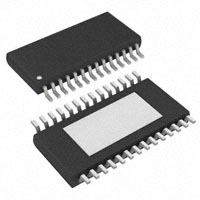
BUF16821 is offered in a HTSSOP-28 PowerPAD™
package, and is specified from –40°C to +85°C.
TFT-LCD REFERENCE DRIVERS
BKSEL
The final gamma and VCOM values can be stored in
the on-chip, nonvolatile memory. To allow for
programming errors or liquid crystal display (LCD)
panel rework, the BUF16821 supports up to 16 write
operations to the on-chip memory.
Analog
(9V to 20V)
1
RELATED PRODUCTS
OUT1
DAC Registers
¼
¼
¼
¼
¼
DAC Registers
16x Nonvolatile Memory BANK0
16x Nonvolatile Memory BANK1
OUT2
OUT15
OUT16
FEATURES
PRODUCT
22-Channel Gamma Correction Buffer
BUF22821
12-Channel Gamma Correction Buffer
BUF12800
18-/20-Channel Programmable Buffer, 10-Bit, VCOM
BUF20800
18-/20-Channel Programmable Buffer with Memory
BUF20820
Programmable VCOM Driver
BUF01900
18V Supply, Traditional Gamma Buffers
BUF11704
22V Supply, Traditional Gamma Buffers
BUF11705
VCOM1
VCOM2
SDA
SCL
Control IF
BUF16821
A0
1
2
3
4
Please be aware that an important notice concerning availability, standard warranty, and use in critical applications of Texas
Instruments semiconductor products and disclaimers thereto appears at the end of this data sheet.
PowerPAD is a trademark of Texas Instruments.
2
I C is a trademark of NXP Semiconductors.
All other trademarks are the property of their respective owners.
PRODUCTION DATA information is current as of publication date.
Products conform to specifications per the terms of the Texas
Instruments standard warranty. Production processing does not
necessarily include testing of all parameters.
Copyright © 2008–2011, Texas Instruments Incorporated
�BUF16821
SBOS428C – JULY 2008 – REVISED JULY 2011
www.ti.com
This integrated circuit can be damaged by ESD. Texas Instruments recommends that all integrated circuits be handled with
appropriate precautions. Failure to observe proper handling and installation procedures can cause damage.
ESD damage can range from subtle performance degradation to complete device failure. Precision integrated circuits may be more
susceptible to damage because very small parametric changes could cause the device not to meet its published specifications.
PACKAGE/ORDERING INFORMATION (1)
(1)
PRODUCT
PACKAGE
PACKAGE DESIGNATOR
BUF16821A
HTSSOP-28
PWP
PACKAGE MARKING
BUF16821
BUF16821B
HTSSOP-28
PWP
BUF16821B
For the most current package and ordering information see the Package Option Addendum at the end of this document, or see the TI
web site at www.ti.com.
ABSOLUTE MAXIMUM RATINGS (1)
Over operating free-air temperature range (unless otherwise noted).
BUF16821
UNIT
Supply Voltage
PARAMETER
VS
+22
V
Supply Voltage
VSD
+6
V
–0.5 to +6
V
±10
mA
(V–) – 0.5 to (V+) + 0.5
V
Digital Input Pins, SCL, SDA, AO, BKSEL: Voltage
Digital Input Pins, SCL, SDA, AO, BKSEL: Current
Output Pins, OUT1 through OUT16, VCOM1 and VCOM2 (2)
Output Short-Circuit (3)
Continuous
Ambient Operating Temperature
–40 to +95
°C
Ambient Storage Temperature
–65 to +150
°C
TJ
+125
°C
Human Body Model
(HBM)
3000
V
Charged Device Model
(CDM)
1000
V
(MM)
200
V
Junction Temperature
ESD Rating
Machine Model
(1)
(2)
(3)
2
Stresses above these ratings may cause permanent damage. Exposure to absolute maximum conditions for extended periods may
degrade device reliability. These are stress ratings only, and functional operation of the device at these or any other conditions beyond
those specified is not supported.
See the Output Protection section.
Short-circuit to ground, one amplifier per package.
Copyright © 2008–2011, Texas Instruments Incorporated
�BUF16821
SBOS428C – JULY 2008 – REVISED JULY 2011
www.ti.com
ELECTRICAL CHARACTERISTICS
Boldface limits apply over the specified temperature range, TA = –40°C to +85°C.
At TA = +25°C, VS = +18V, VSD = +2V, RL = 1.5kΩ connected to ground, and CL = 200pF, unless otherwise noted.
BUF16821
PARAMETER
CONDITIONS
MIN
TYP
17.7
17.85
MAX
UNIT
ANALOG GAMMA BUFFER CHANNELS
Reset Value
Code 512
OUT 1–16 Output Swing: High
Code = 1023, Sourcing 10mA
OUT 1–16 Output Swing: Low
Code = 0, Sinking 10mA
9
0.07
V
V
0.3
V
VCOM1, 2 Output Swing: High
BUF16821A
Code = 1023, Sourcing 100mA
BUF16821B (1)
Code = 511, Sourcing 100mA
13
16.2
V
8.96
V
VCOM1, 2 Output Swing: Low
BUF16821A
BUF16821B (1)
Continuous Output Current
Code = 0, Sinking 100mA
0.6
Code = 384, Sinking 100mA
6.75
V
30
mA
Note
(2)
±20
Output Accuracy
vs Temperature
Integral Nonlinearity
Code 512
INL
Differential Nonlinearity
DNL
Load Regulation, 10mA
REG
2
±50
mV
±25
μV/°C
0.3
LSB
0.3
Code 512 or VCC/2, IOUT = +5mA to –5mA Step
V
0.5
LSB
1.5
mV/mA
16
Cycles
OTP MEMORY
Number of OTP Write Cycles
Memory Retention
100
Years
ANALOG POWER SUPPLY
Operating Range
Total Analog Supply Current
9
IS
Outputs at Reset Values, No Load
12
Over Temperature
20
V
14
mA
18
mA
DIGITAL
Logic 1 Input Voltage
VIH
Logic 0 Input Voltage
VIL
Logic 0 Output Voltage
0.7 × VSD
VOL
ISINK = 3mA
Input Leakage
Clock Frequency
V
0.3 × VSD
fCLK
V
0.15
0.4
V
±0.01
±10
μA
Standard/Fast Mode
400
kHz
High-Speed Mode
3.4
MHz
DIGITAL POWER SUPPLY
Operating Range
Digital Supply Current (2)
VSD
ISD
2.0
Outputs at Reset Values, No Load, Two-Wire Bus Inactive
115
Over Temperature
5.5
V
150
μA
μA
115
TEMPERATURE RANGE
Specified Range
Junction Temperature < +125°C
Operating Range
Storage Range
Thermal Resistance (2)
+85
°C
–40
+95
°C
–65
+150
°C
θJA
HTSSOP-28
(1)
(2)
(3)
–40
See Note
(3)
40
°C/W
BUF16821B output swing is limited internally. Bits 9, 8, and 7 are fixed at '011'.
Observe maximum power dissipation.
Thermal pad attached to printed circuit board (PCB), 0lfm airflow, and 76mm × 76mm copper area.
Copyright © 2008–2011, Texas Instruments Incorporated
3
�BUF16821
SBOS428C – JULY 2008 – REVISED JULY 2011
www.ti.com
PIN CONFIGURATION
PWP PACKAGE
HTSSOP-28
(TOP VIEW)
VCOM2
1
28
VCOM1
OUT1
2
27
OUT16
OUT2
3
26
OUT15
OUT3
4
25
OUT14
OUT4
5
24
GNDA
OUT5
6
23
VS
OUT6
7
22
OUT13
(1)
GNDA
8
21
OUT12
VS
9
20
OUT11
OUT7
10
19
OUT10
OUT8
11
18
GNDD
OUT9
12
17
BKSEL
VSD
13
16
A0
SCL
14
15
SDA
PowerPAD
Lead-Frame
Die Pad
Exposed on
Underside
(must connect to
GNDA and GNDD)
(1)
(1)
NOTE: (1) GNDA and GNDD must be connected together.
4
Copyright © 2008–2011, Texas Instruments Incorporated
�BUF16821
SBOS428C – JULY 2008 – REVISED JULY 2011
www.ti.com
PIN DESCRIPTIONS
PIN #
NAME
DESCRIPTION
1
VCOM2
VCOM channel 2
2
OUT1
DAC output 1
3
OUT2
DAC output 2
4
OUT3
DAC output 3
5
OUT4
DAC output 4
6
OUT5
DAC output 5
7
OUT6
DAC output 6
8
GNDA
Analog ground; must be connected to digital ground (GNDD).
9
VS
10
OUT7
DAC output 7
11
OUT8
DAC output 8
12
OUT9
DAC output 9
13
VSD
Digital supply; connect to logic supply
14
SCL
Serial clock input; open-drain, connect to pull-up resistor.
15
SDA
Serial data I/O; open-drain, connect to pull-up resistor.
16
A0
17
BKSEL
Selects memory bank 0 or 1; connect to either logic 1 to select bank 1 or logic 0 to select bank 0.
18
GNDD
Digital ground; must be connected to analog ground at the BUF16821.
19
OUT10
DAC output 10
20
OUT11
DAC output 11
21
OUT12
DAC output 12
22
OUT13
DAC output 13
23
VS
VS connected to analog supply
A0 address pin for I2C address; connect to either logic 1 or logic 0. See Table 1.
VS connected to analog supply
24
GNDA
Analog ground; must be connected to digital ground (GNDD).
25
OUT14
DAC output 14
26
OUT15
DAC output 15
27
OUT16
DAC output 16
28
VCOM1
VCOM channel 1
Copyright © 2008–2011, Texas Instruments Incorporated
5
�BUF16821
SBOS428C – JULY 2008 – REVISED JULY 2011
www.ti.com
TYPICAL CHARACTERISTICS
At TA = +25°C, VS = +18V, VSD = +2V, RL = 1.5kΩ connected to ground, and CL = 200pF, unless otherwise noted.
18.0
17.5
17.0
16.5
16.0
15.5
15.0
OUTPUT VOLTAGE vs OUTPUT CURRENT
(Channels 1–16)
VCOM1
3.0
2.5
2.0
1.5
1.0
0.5
0
Output Voltage (V)
Output Voltage (V)
OUTPUT VOLTAGE vs OUTPUT CURRENT
(VCOM1 and VCOM2)
VCOM2
0
25
50
75
100
125
18.0
17.5
17.0
16.5
16.0
15.5
15.0
3.0
2.5
2.0
1.5
1.0
0.5
0
Output Swing High
Output Swing Low
150
0
25
50
Output Current (mA)
Figure 1.
125
100
150
Figure 2.
DIGITAL SUPPLY CURRENT vs TEMPERATURE
ANALOG SUPPLY CURRENT vs TEMPERATURE
120
11.0
118
10.5
Analog Supply Current (mA)
Digital Supply Current (mA)
75
Output Current (mA)
116
114
112
110
108
106
104
10.0
9.5
9.0
8.5
8.0
7.5
7.0
102
100
6.5
-50
-25
0
25
50
75
100
125
-50
-25
0
Temperature (°C)
25
50
75
100
125
Temperature (°C)
Figure 3.
Figure 4.
OUTPUT VOLTAGE vs TEMPERATURE
DIFFERENTIAL LINEARITY ERROR
9.020
0.15
10 Typical Units Shown
9.015
0.10
9.005
Error (LSB)
Initial Voltage (V)
9.010
9.000
8.995
0.05
0
-0.05
8.990
-0.10
8.985
8.980
-0.15
-50
-25
0
25
50
Temperature (°C)
Figure 5.
6
75
100
125
0
256
512
768
1024
Input Code
Figure 6.
Copyright © 2008–2011, Texas Instruments Incorporated
�BUF16821
SBOS428C – JULY 2008 – REVISED JULY 2011
www.ti.com
TYPICAL CHARACTERISTICS (continued)
At TA = +25°C, VS = +18V, VSD = +2V, RL = 1.5kΩ connected to ground, and CL = 200pF, unless otherwise noted.
INTEGRAL LINEARITY ERROR
BKSEL SWITCHING TIME DELAY
0.15
0.10
Error (LSB)
BKSEL (2V/div)
0.05
780ms
0
9V
-0.05
DAC Channel
(2V/div)
-0.10
5V
-0.15
0
256
768
512
1ms/div
1024
Input Code
Figure 7.
Figure 8.
Output Voltage (2V/div)
LARGE-SIGNAL STEP RESPONSE
Time (2ms/div)
Figure 9.
Copyright © 2008–2011, Texas Instruments Incorporated
7
�BUF16821
SBOS428C – JULY 2008 – REVISED JULY 2011
www.ti.com
APPLICATION INFORMATION
GENERAL
The BUF16821 programmable voltage reference
allows fast and easy adjustment of 16 programmable
gamma reference outputs and two VCOM outputs,
each with 10-bit resolution. The BUF16821 is
programmed through a high-speed, I2C interface. The
final gamma and VCOM values can be stored in the
onboard, nonvolatile memory. To allow for
programming errors or liquid crystal display (LCD)
panel rework, the BUF16821 supports up to 16 write
operations to the onboard memory. The BUF16821
has two separate memory banks, allowing
simultaneous storage of two different gamma curves
to facilitate dynamic switching between gamma
curves.
The BUF16821 can be powered using an analog
supply voltage from 9V to 20V, and a digital supply
from 2V to 5.5V. The digital supply must be applied
before the analog supply to avoid excessive current
and power consumption, or possibly even damage to
the device if left connected only to the analog supply
for extended periods of time. Figure 10 illustrates a
typical configuration of the BUF16821.
TWO-WIRE BUS OVERVIEW
The
BUF16821
communicates
over
an
industry-standard, two-wire interface to receive data
in slave mode. This standard uses a two-wire,
open-drain interface that supports multiple devices on
a single bus. Bus lines are driven to a logic low level
only. The device that initiates the communication is
called a master, and the devices controlled by the
master are slaves. The master generates the serial
clock on the clock signal line (SCL), controls the bus
access, and generates the START and STOP
conditions.
To address a specific device, the master initiates a
START condition by pulling the data signal line (SDA)
from a HIGH to a LOW logic level while SCL is HIGH.
All slaves on the bus shift in the slave address byte
on the rising edge of SCL, with the last bit indicating
whether a read or write operation is intended. During
the ninth clock pulse, the slave being addressed
responds to the master by generating an
Acknowledge and pulling SDA LOW.
Data transfer is then initiated and eight bits of data
are sent, followed by an Acknowledge bit. During
data transfer, SDA must remain stable while SCL is
HIGH. Any change in SDA while SCL is HIGH is
interpreted as a START or STOP condition.
Once all data have been transferred, the master
generates a STOP condition, indicated by pulling
SDA from LOW to HIGH while SCL is HIGH. The
BUF16821 can act only as a slave device; therefore,
it never drives SCL. SCL is an input only for the
BUF16821.
ADDRESSING THE BUF16821
The address of the BUF16821 is 111010x, where x is
the state of the A0 pin. When the A0 pin is LOW, the
device acknowledges on address 74h (1110100). If
the A0 pin is HIGH, the device acknowledges on
address 75h (1110101). Table 1 shows the A0 pin
settings and BUF16821 address options.
Other valid addresses are possible through a simple
mask change. Contact your TI representative for
information.
Table 1. Quick-Reference of BUF16821 Addresses
DEVICE/COMPONENT
BUF16821 Address
ADDRESS
A0 pin is LOW
(device acknowledges on address 74h)
1110100
A0 pin is HIGH
(device acknowledges on address 75h)
1110101
Table 2. Quick-Reference of Command Codes
8
COMMAND
CODE
General-Call Reset
Address byte of 00h followed by a data byte of 06h.
High-Speed Mode
00001xxx, with SCL ≤ 400kHz; where xxx are bits unique to the Hs-capable master. This
byte is called the Hs master code.
Copyright © 2008–2011, Texas Instruments Incorporated
�BUF16821
SBOS428C – JULY 2008 – REVISED JULY 2011
www.ti.com
BUF16821
(1)
(1)
VCOM2
1
VCOM2
VCOM1
28
2
OUT1
OUT16
27
3
OUT2
OUT15
26
4
OUT3
OUT14
25
5
OUT4
6
OUT5
7
OUT6
8
GNDA
VCOM1
(1)
(1)
(1)
(1)
(1)
(1)
Source
Driver
(1)
(1)
GNDA
(2)
24
VS
23
OUT13
22
OUT12
21
100nF
(1)
10mF
100nF
(2)
(1)
9
VS
OUT11
20
10
OUT7
OUT10
19
11
OUT8
12
OUT9
13
14
10mF
(1)
Source
Driver
(1)
(1)
Source
Driver
VS
(1)
(1)
VS
Source
Driver
GNDD
(2)
18
(1)
3.3V
1mF
100nF
BKSEL
17
VSD
A0
16
SCL
SDA
15
Timing
Controller
(1)
RC combination optional; see the Output Protection section.
(2)
GNDA and GNDD must be connected together.
Figure 10. Typical Application Configuration
Copyright © 2008–2011, Texas Instruments Incorporated
9
�BUF16821
SBOS428C – JULY 2008 – REVISED JULY 2011
www.ti.com
DATA RATES
OUTPUT VOLTAGE
The two-wire bus operates in one of three speed
modes:
• Standard: allows a clock frequency of up to
100kHz;
• Fast: allows a clock frequency of up to 400kHz;
and
• High-speed mode (also called Hs mode): allows a
clock frequency of up to 3.4MHz.
Buffer output values are determined by the analog
supply voltage (VS) and the decimal value of the
binary input code used to program that buffer. The
value is calculated using Equation 1:
CODE10
VOUT = VS ´
1024
The BUF16821 is fully compatible with all three
modes. No special action is required to use the
device in Standard or Fast modes, but High-speed
mode must be activated. To activate High-speed
mode, send a special address byte of 00001 xxx, with
SCL ≤ 400kHz, following the START condition; where
xxx are bits unique to the Hs-capable master, which
can be any value. This byte is called the Hs master
code. Table 2 provides a reference for the
High-speed mode command code. (Note that this
configuration is different from normal address
bytes—the low bit does not indicate read/write
status.) The BUF16821 responds to the High-speed
command regardless of the value of these last three
bits. The BUF16821 does not acknowledge this byte;
the
communication
protocol
prohibits
acknowledgment of the Hs master code. Upon
receiving a master code, the BUF16821 switches on
its Hs mode filters, and communicates at up to
3.4MHz. Additional high-speed transfers may be
initiated without resending the Hs mode byte by
generating a repeat START without a STOP. The
BUF16821 switches out of Hs mode with the next
STOP condition.
GENERAL-CALL RESET AND POWER-UP
The BUF16821 responds to a General-Call Reset,
which is an address byte of 00h (0000 0000) followed
by a data byte of 06h (0000 0110). The BUF16821
acknowledges both bytes. Table 2 provides a
reference for the General-Call Reset command code.
Upon receiving a General-Call Reset, the BUF16821
performs a full internal reset, as though it had been
powered off and then on. It always acknowledges the
General-Call address byte of 00h (0000 0000), but
does not acknowledge any General-Call data bytes
other than 06h (0000 0110).
When the BUF16821 powers up, it automatically
performs a reset. As part of the reset, the BUF16821
is configured for all outputs to change to the last
programmed nonvolatile memory values, or
1000000000 if the nonvolatile memory values have
not been programmed.
10
(1)
The BUF16821 outputs are capable of a full-scale
voltage output change in typically 5μs; no
intermediate steps are required.
UPDATING THE DAC OUTPUT VOLTAGES
Because the BUF16821 features a double-buffered
register structure, updating the digital-to-analog
converter (DAC) and/or the VCOM register is not the
same as updating the DAC and/or VCOM output
voltage. There are two methods for updating the
DAC/VCOM output voltages.
Method 1: Method 1 is used when it is desirable to
have the DAC/VCOM output voltage change
immediately after writing to a DAC register. For each
write transaction, the master sets data bit 15 to a '1'.
The DAC/VCOM output voltage update occurs after
receiving the 16th data bit for the currently-written
register.
Method 2: Method 2 is used when it is desirable to
have all DAC/VCOM output voltages change at the
same time. First, the master writes to the desired
DAC/VCOM channels with data bit 15 a '0'. Then,
when writing the last desired DAC/VCOM channel, the
master sets data bit 15 to a '1'. All DAC/VCOM
channels are updated at the same time after
receiving the 16th data bit.
NONVOLATILE MEMORY
BKSEL Pin
The BUF16821 has 16x rewrite capability of the
nonvolatile memory. Additionally, the BUF16821 has
the ability to store two distinct gamma curves in two
different nonvolatile memory banks, each of which
has 16x rewrite capability. One of the two available
banks is selected using the external input pin,
BKSEL. When this pin is low, BANK0 is selected;
when this pin is high, BANK1 is selected.
Copyright © 2008–2011, Texas Instruments Incorporated
�BUF16821
SBOS428C – JULY 2008 – REVISED JULY 2011
www.ti.com
When the BKSEL pin changes state, the BUF16821
acquires the last programmed DAC/VCOM values from
the nonvolatile memory associated with this newly
chosen bank. At power-up, the state of the BKSEL
pin determines which memory bank is selected.
The I2C master also has the ability to update
(acquire) the DAC registers with the last programmed
nonvolatile memory values using software control.
The bank to be acquired depends on the state of
BKSEL.
General Acquire Command
A general acquire command is used to update all
registers and DAC/VCOM outputs to the last
programmed values stored in nonvolatile memory. A
single-channel acquire command updates only the
register and DAC/VCOM output of the DAC/VCOM
corresponding to the DAC/VCOM address used in the
single-channel acquire command.
These are the steps of the sequence to initiate a
general channel acquire:
1. Be sure BKSEL is in its desired state and has
been stable for at least 1ms.
2. Send a START condition on the bus.
3. Send the appropriate device address (based on
A0) and the read/write bit = LOW. The BUF16821
acknowledges this byte.
4. Send a DAC/VCOM pointer address byte. Set bit
D7 = 1 and D6 = 0. Bits D5–D0 are any valid
DAC/VCOM address. Although the BUF16821
acknowledges 000000 through 010111, it stores
and returns data only from these addresses:
– 000000 through 001111
– 010010 and 010011
It returns 0000 for reads from 010000 and
010001, and 010100 through 010111. See
Table 4 for valid DAC/VCOM addresses.
5. Send a STOP condition on the bus.
Approximately 750μs (±80μs) after issuing this
command, all DAC/VCOM registers and DAC/VCOM
output voltages change to the respective, appropriate
nonvolatile memory values.
xxx
xxx
Single-Channel Acquire Command
These are the steps to initiate a single-channel
acquire:
1. Be sure BKSEL is in its desired state and has
been stable for at least 1ms.
2. Send a START condition on the bus.
3. Send the device address (based on A0) and
read/write bit = LOW. The BUF16821
acknowledges this byte.
4. Send a DAC/VCOM pointer address byte using the
DAC/VCOM address corresponding to the output
and register to update with the OTP memory
value. Set bit D7 = 0 and D6 = 1. Bits D5–D0 are
the DAC/VCOM address. Although the BUF16821
acknowledges 000000 through 010111, it stores
and returns data only from these addresses:
– 000000 through 001111
– 010010 and 010011
It returns 0000 reads from 010000 and 010001,
and 010100 through 010111. See Table 4 for
valid DAC/VCOM addresses.
5. Send a STOP condition on the bus.
Approximately 36μs (±4μs) after issuing this
command, the specified DAC/VCOM register and
DAC/VCOM output voltage change to the appropriate
OTP memory value.
MaxBank
The BUF16821 can provide the user with the number
of times the nonvolatile memory of a particular
DAC/VCOM channel nonvolatile memory has been
written to for the current memory bank. This
information is provided by reading the register at
pointer address 111111.
There are two ways to update the MaxBank register:
1. After initiating a single acquire command, the
BUF16821 updates the MaxBank register with a
code corresponding to how many times that
particular channel memory has been written to.
2. Following a general acquire command, the
BUF16821 updates the MaxBank register with a
code corresponding to the maximum number of
times the most used channel (OUT1–16 and
VCOMs) has been written to.
MaxBank is a read-only register and is only updated
by performing a general- or single-channel acquire.
Copyright © 2008–2011, Texas Instruments Incorporated
11
�BUF16821
SBOS428C – JULY 2008 – REVISED JULY 2011
www.ti.com
Table 3 shows the relationship between the number
of times the nonvolatile memory has been
programmed and the corresponding state of the
MaxBank Register.
Table 3. MaxBank Details
READ/WRITE OPERATIONS
Read and write operations can be done for a single
DAC/VCOM or for multiple DACs/VCOMs. Writing to a
DAC/VCOM register differs from writing to the
nonvolatile memory. Bits D15–D14 of the most
significant byte of data determines if data are written
to the DAC/VCOM register or the nonvolatile memory.
NUMBER OF TIMES WRITTEN TO
RETURNS CODE
0
0000
1
0000
Read/Write: DAC/VCOM Register (volatile memory)
2
0001
3
0010
4
0011
5
0100
6
0101
7
0110
8
0111
9
1000
The BUF16821 is able to read from a single
DAC/VCOM, or multiple DACs/VCOMs, or write to the
register of a single DAC/VCOM, or multiple
DACs/VCOMs in a single communication transaction.
DAC pointer addresses begin with 000000 (which
corresponds to OUT1) through 001111 (which
corresponds to OUT16). Addresses 010010 and
010011 are VCOM1 and VCOM2, respectively.
10
1001
11
1010
12
1011
13
1100
14
1101
15
1110
16
1111
Parity Error Correction
The BUF16821 provides single-bit parity error
correction for data stored in the nonvolatile memory
to provide increased reliability of the nonvolatile
memory. If a single bit of nonvolatile memory for a
channel fails, the BUF16821 corrects for it and
updates the appropriate DAC with the intended value
when its memory is acquired.
If more than one bit of nonvolatile memory for a
channel fails, the BUF16821 does not correct for it,
and updates the appropriate DAC/VCOM with the
default value of 1000000000.
DIE_ID AND DIE_REV REGISTERS
The user can verify the presence of the BUF16821 in
the system by reading from address 111101. When
read at this address, the BUF16821A returns
0101100100100111 and the BUF16821B returns
0101100100100100.
Write commands are performed by setting the
read/write bit LOW. Setting the read/write bit HIGH
performs a read transaction.
Writing: DAC/VCOM Register (Volatile Memory)
To write to a single DAC/VCOM register:
1. Send a START condition on the bus.
2. Send the device address and read/write bit =
LOW. The BUF16821 acknowledges this byte.
3. Send a DAC/VCOM pointer address byte. Set bit
D7 = 0 and D6 = 0. Bits D5–D0 are the
DAC/VCOM address. Although the BUF16821
acknowledges 000000 through 010111, it stores
and returns data only from these addresses:
– 000000 through 001111
– 010010 through 010011
It returns 0000 for reads from 010000 through
010001, and 010100 through 010111. See
Table 4 for valid DAC/VCOM addresses.
4. Send two bytes of data for the specified register.
Begin by sending the most significant byte first
(bits D15–D8, of which only bits D9 and D8 are
used, and bits D15–D14 must not be 01),
followed by the least significant byte (bits
D7–D0). The register is updated after receiving
the second byte.
5. Send a STOP or START condition on the bus.
The user can also determine the die revision of the
BUF16821 by reading from register 111100.
BUF16821 returns 0000000000000000 when a RevA
die is present. RevB would be designated by
0000000000000001 and so on.
12
Copyright © 2008–2011, Texas Instruments Incorporated
�BUF16821
www.ti.com
The BUF16821 acknowledges each data byte. If the
master terminates communication early by sending a
STOP or START condition on the bus, the specified
register is not updated. Updating the DAC/VCOM
register is not the same as updating the DAC/VCOM
output voltage; see the Updating the DAC Outputs
section.
The process of updating multiple DAC/VCOM registers
begins the same as when updating a single register.
However, instead of sending a STOP condition after
writing the addressed register, the master continues
to send data for the next register. The BUF16821
automatically and sequentially steps through
subsequent registers as additional data are sent. The
process continues until all desired registers have
been updated or a STOP or START condition is sent.
To write to multiple DAC/VCOM registers:
1. Send a START condition on the bus.
2. Send the device address and read/write bit =
LOW. The BUF16821 acknowledges this byte.
3. Send either the OUT1 pointer address byte to
start at the first DAC, or send the pointer address
byte for whichever DAC/VCOM is the first in the
sequence of DACs/VCOMs to be updated. The
BUF16821 begins with this DAC/VCOM and steps
through subsequent DACs/VCOMs in sequential
order.
4. Send the bytes of data; begin by sending the
most significant byte (bits D15–D8, of which only
bits D9 and D8 have meaning, and bits D15–D14
must not be 01), followed by the least significant
byte (bits D7–D0). The first two bytes are for the
DAC/VCOM addressed in the previous step. The
DAC/VCOM register is automatically updated after
receiving the second byte. The next two bytes are
for the following DAC/VCOM. That DAC/VCOM
register is updated after receiving the fourth byte.
This process continues until the registers of all
following DACs/VCOMs have been updated. The
BUF16821 continues to accept data for a total of
18 DACs; however, the two data sets following
the 16th data set are meaningless. The 19th and
20th data sets apply to VCOM1 and VCOM2. The
write disable bit cannot be accessed using this
method. It must be written to using the write to a
single DAC register procedure.
Copyright © 2008–2011, Texas Instruments Incorporated
SBOS428C – JULY 2008 – REVISED JULY 2011
5. Send a STOP or START condition on the bus.
The BUF16821 acknowledges each byte. To
terminate communication, send a STOP or START
condition on the bus. Only DAC registers that have
received both bytes of data are updated.
Reading: DAC/VCOM/OTHER Register (Volatile
Memory)
Reading a register returns the data stored in that
DAC/VCOM/OTHER register.
To read a single DAC/VCOM/OTHER register:
1. Send a START condition on the bus.
2. Send the device address and read/write bit =
LOW. The BUF16821 acknowledges this byte.
3. Send the DAC/VCOM/OTHER pointer address
byte. Set bit D7 = 0 and D6 = 0; bits D5–D0 are
the DAC/VCOM/OTHER address. NOTE: The
BUF16821 stores and returns data only from
these addresses:
– 000000 through 001111
– 010010
– 010011
– 111100 through 111111
It returns 0000 for reads from 010000 and
010001, and 010100 through 010111. See
Table 4 for valid DAC/VCOM/OTHER addresses.
4. Send a START or STOP/START condition.
5. Send the correct device address and read/write
bit = HIGH. The BUF16821 acknowledges this
byte.
6. Receive two bytes of data. They are for the
specified register. The most significant byte (bits
D15–D8) is received first; next is the least
significant byte (bits D7–D0). In the case of
DAC/VCOM channels, bits D15–D10 have no
meaning.
7. Acknowledge after receiving the first byte.
8. Send a STOP or START condition on the bus or
do not acknowledge the second byte to end the
read transaction.
13
�BUF16821
SBOS428C – JULY 2008 – REVISED JULY 2011
Communication may be terminated by sending a
premature STOP or START condition on the bus, or
by not acknowledging.
To read multiple registers:
1. Send a START condition on the bus.
2. Send the device address and read/write bit =
LOW. The BUF16821 acknowledges this byte.
3. Send either the OUT1 pointer address byte to
start at the first DAC, or send the pointer address
byte for whichever register is the first in the
sequence of DACs/VCOMs to be read. The
BUF16821 begins with this DAC/VCOM and steps
through subsequent DACs/VCOMs in sequential
order.
4. Send a START or STOP/START condition on the
bus.
5. Send the correct device address and read/write
bit = HIGH. The BUF16821 acknowledges this
byte.
6. Receive two bytes of data. They are for the
specified DAC/VCOM. The first received byte is the
most significant byte (bits D15–D8; only bits D9
and D8 have meaning), next is the least
significant byte (bits D7–D0).
7. Acknowledge after receiving each byte of data.
8. When all desired DACs have been read, send a
STOP or START condition on the bus.
Communication may be terminated by sending a
premature STOP or START condition on the bus, or
by not sending the acknowledge bit. The reading of
registers DieID, DieRev, and MaxBank is not
supported in this mode of operation (these values
must be read using the single register read method).
Write: Nonvolatile Memory for the DAC Register
The BUF16821 is able to write to the nonvolatile
memory of a single DAC/VCOM in a single
communication transaction. In contrast to the
BUF20820, writing to multiple nonvolatile memory
words in a single transaction is not supported. Valid
DAC/VCOM pointer addresses begin with 000000
(which corresponds to OUT1) through 001111 (which
corresponds to OUT16). Addresses 010010 and
010011 are VCOM1 and VCOM2, respectively.
When programming the nonvolatile memory, the
analog supply voltage must be between 9V and 20V.
Write commands are performed by setting the
read/write bit LOW.
14
www.ti.com
To write to a single nonvolatile register:
1. Send a START condition on the bus.
2. Send the device address and read/write bit =
LOW. The BUF16821 acknowledges this byte.
Although the BUF16821 acknowledges 000000
through 010111, it stores and returns data only
from these addresses:
– 000000 through 001111
– 010010 and 010011
It returns 0000 for reads from 010000 through
010001, and 010100 through 010111. See
Table 4 for DAC/VCOM addresses.
3. Send a DAC/VCOM pointer address byte. Set bit
D7 = 0 and D6 = 0. Bits D5–D0 are the
DAC/VCOM address.
4. Send two bytes of data for the nonvolatile register
of the specified DAC/VCOM. Begin by sending the
most significant byte first (bits D15–D8, of which
only bits D9 and D8 are data bits, and bits
D15–D14 must be 01), followed by the least
significant byte (bits D7–D0). The register is
updated after receiving the second byte.
5. Send a STOP condition on the bus.
The BUF16821 acknowledges each data byte. If the
master terminates communication early by sending a
STOP or START condition on the bus, the specified
nonvolatile register is not updated. Writing a
nonvolatile register also updates the DAC/VCOM
register and output voltage.
The DAC/VCOM register and DAC/VCOM output voltage
are updated immediately, while the programming of
the nonvolatile memory takes up to 250μs. Once a
nonvolatile register write command has been issued,
no communication with the BUF16821 should take
place for at least 250μs. Writing or reading over the
serial interface while the nonvolatile memory is being
written jeopardizes the integrity of the data being
stored.
Read: Nonvolatile Memory for the DAC Register
To read the data present in nonvolatile register for a
particular DAC/VCOM channel, the master must first
issue a general acquire command, or a single acquire
command with the appropriate DAC/VCOM channel
chosen. This action updates both the DAC/VCOM
register(s) and DAC/VCOM output voltage(s). The
master may then read from the appropriate
DAC/VCOM register as described earlier.
Copyright © 2008–2011, Texas Instruments Incorporated
�BUF16821
SBOS428C – JULY 2008 – REVISED JULY 2011
www.ti.com
Table 4. DAC Register Pointer Addresses
DAC REGISTER
POINTER ADDRESS
OUT1
000000
OUT2
000001
OUT3
000010
OUT4
000011
OUT5
000100
OUT6
000101
OUT7
000110
OUT8
000111
OUT9
001000
OUT10
001001
OUT11
001010
OUT12
001011
OUT13
001100
OUT14
001101
OUT15
001110
OUT16
001111
VCOM1
010010
VCOM2
010011
OTHER REGISTER
POINTER ADDRESS
Die_Rev
111100
Die_ID
111101
MaxBank
111111
Copyright © 2008–2011, Texas Instruments Incorporated
15
�16
Figure 11. Write DAC Register Timing
A6
A6
A6
SDA_In
Start
Device_Out
SCL
A4
A4
A3
A3
A5
A5
A4
A4
A5
A5
A4
A4
A3
A3
Device Address
A2
A2
A5
A5
A4
A4
A3
A3
Device Address
A2
A2
A1
A1
A1
A1
A3
A3
Device Address
Read multiple DAC registers. P4-P0 specify DAC address.
A6
SDA_In
Start
Device_Out
SCL
A5
A5
Read single DAC register. P4-P0 specify DAC address.
A6
A6
SDA_In
Start
Device_Out
SCL
A6
Device_Out
Device Address
A2
A2
A1
A1
A0
A0
A0
A0
A2
A2
W
W
Write
W
W
Write
A1
A1
A0
A0
A0
A0
D7
D7
Ackn
Ackn
Ackn
D7
D7
Read operation.
Ackn
Ackn
Ackn
W
W
Write
W
W
Write
Read operation.
Write multiple DAC registers. P4-P0 specify DAC address.
A6
SDA_In
SCL
Start
Write single DAC register. P4-P0 specify DAC address.
D7
D7
D7
D7
D5
D5
D6
D6
D5
D5
D5
D5
P4
P4
P3
P3
P2
P2
P4
D6
D6
D5
D5
P4
P4
P3
P3
P2
P2
P1
P1
P1
P1
P4
Start DAC address pointer. D7-D5 must be 000.
D6
D6
P4
P4
P3
P3
P2
P2
P0
P0
P0
P0
P3
P3
Ackn
Ackn
Ackn
Ackn
Ackn
Ackn
P2
P2
P1
P1
P1
P1
Start
Start
DAC address pointer. D7-D5 must be 000.
D6
D6
DAC address pointer. D7-D5 must be 000.
DAC address pointer. D7-D5 must be 000.
Ackn
Ackn
Ackn
Write Operation
Ackn
Ackn
Ackn
Write Operation
D14
D14
D15
D14
D14
A3
A3
A4
A3
A3
Device Address
A4
D14
D14
D15
D13
D13
D11
D11
D10
D10
D13
D13
D12
D12
D11
D11
D10
D10
DAC (pointer) MSbyte. D14 must be 0.
Device Address
A4
D12
D12
D9
D9
D8
D8
Ackn
Ackn
D7
D7
D9
D9
D8
D8
Ackn
Ackn
Ackn
D7
D7
A2
A2
A2
A2
A1
A1
A1
A1
A0
A0
A0
A0
D12
D12
D11
D11
D10
D10
D9
D9
D8
D8
R
R
Read
R
R
Ackn
Ackn
Ackn
Ackn
Ackn
Ackn
Ackn
D7
D7
D15
D15
D15
D11
D11
D10
D10
D9
D9
D6
D6
D6
D6
D8
D8
D13
D12
D12
D11
D11
D10
D10
D14
D6
D6
D14
D13
D5
D5
D13
D12
D11
D11
D4
D4
D3
D3
DAC 20 LSbyte.
D12
D10
D2
D2
D10
D4
D4
D3
D3
DAC LSbyte
D9
D9
Ackn
Ackn
Ackn
D5
D5
D9
D1
D1
D9
D0
D0
D8
D8
D8
D8
D4
D4
Ackn
D1
D1
D0
D0
Ackn
Ackn
Ackn
D2
D1
D1
D0
D0
Ackn
Ackn
D7
D7
D6
D6
D5
D5
D5
D5
D4
D4
D2
D2
D4
D4
D3
D3
DAC LSbyte.
D3
D3
DAC 20 LSbyte
is updated at this moment.
Stop
D2
D2
D1
D1
D15
D15
D1
D1
D14
D14
D0
D0
D0
D0
Stop
Stop
No Ackn
No Ackn
Ackn
Ackn
Ackn
D13
D13
DAC (pointer + 1) MSbyte. D14 must be 0.
The entire DAC register D9-D0
D2
Ackn
is updated at this moment.
The entire DAC register D9-D0
D2
D2
Stop
D6
D6
Ackn
Ackn
Ackn
Ackn
Ackn
Ackn
Ackn
Ackn
D7
D7
D3
D3
DAC (pointer) LSbyte
D5
D5
DAC (pointer) MSbyte. D15-D10 have no meaning.
D14
D13
DAC MSbyte. D15-D10 have no meaning.
D14
D12
D13
D15
D12
D13
Ackn
Ackn
D14
D15
Read
D14
D15
DAC 20 (VCOM OUT2) MSbyte. D14 must be 0.
If D15 = 1, all DACs are updated when the current DAC register is updated.
D15
A4
D13
D13
Ackn
If D15 = 1, all DACs are updated when the current DAC register is updated.
D15
D15
DAC MSbyte. D14 must be 0.
DAC 20 (VCOM OUT2) MSbyte. D15-D10 have no meaning.
A5
A5
A5
A5
Ackn
Ackn
Ackn
Ackn
Ackn
D15
A6
A6
A6
A6
P0
P0
P0
P0
Ackn
BUF16821
SBOS428C – JULY 2008 – REVISED JULY 2011
www.ti.com
Figure 12. Read Register Timing
Copyright © 2008–2011, Texas Instruments Incorporated
�A6
A6
SDA_In
Device_Out
SCL
Start
A5
A5
A4
A4
A3
A3
Device Address
A1
Figure 13. Write Nonvolatile Register Timing
Copyright © 2008–2011, Texas Instruments Incorporated
A0
W
W
Ackn
Ackn
D6
D6
D5
D5
P4
P4
P3
P3
P2
P2
A5
A5
A4
A4
A3
A3
Device address.
A2
A2
A1
A1
P1
A0
A0
P1
A6
A6
SDA_In
Device_Out
Start
A5
A5
A4
A4
A3
A3
Device address.
A2
A2
A1
A1
A0
A0
P0
P0
W
W
Write
W
W
Write
Single channel acquire command. P4-P0 must specify and valid DAC address.
A6
Start
Device_Out
SCL
D7
D7
DAC address pointer. D7-D0 must be 000.
General acquire command. P4-P0 must specify and valid DAC address.
A0
Ackn
Write operation.
A6
SCL
A1
Write
D15
D15
D7
D7
Ackn
Ackn
Ackn
D7
D7
Write Operation
Ackn
Ackn
Ackn
Write Operation
Ackn
Ackn
Ackn
D14
D14
D12
D12
D11
D11
D10
D10
D9
D9
D8
D8
D5
D5
P4
P4
P3
P3
P2
P2
D6
D6
D5
D5
P4
P4
P3
P3
P2
P2
DAC address pointer. D7-D5 must be 010.
D6
D6
DAC address pointer. D7-D5 must be 100.
D13
D13
DAC MSbyte. D15-D14 must be 01.
P1
P1
P1
P1
Ackn
Ackn
Ackn
P0
P0
P0
P0
D7
D6
D6
Ackn
Ackn
Ackn
Ackn
Ackn
Ackn
D7
D5
Stop
Stop
D5
D4
D4
D2
D2
D1
D1
D0
D0
Ackn
Ackn
Ackn
Stop
t2: minimum 100ms, maximum 2ms.
The OTP register (D9-D0) is updated at this moment.
t1: > 20ms before falling edge of clock.
D3
D3
DAC LSbyte.
t2
www.ti.com
SDA_In
A2
A2
Write single OTP register. P4-P0 specify DAC address.
Write supply active.
Write signal active.
t1
BUF16821
SBOS428C – JULY 2008 – REVISED JULY 2011
Figure 14. Acquire Operation Timing
17
�18
Figure 15. General-Call Reset Timing
SDA
SCL
SDA
SCL
Start
High-Speed Command
Start
General-Call Reset Command
Address Byte = 00h
Address Byte = 00001xxx (HS Master Code)
Ackn
Ackn
Device enters high-speed mode at ACK clock pulse.
Device exits high-speed mode with stop condition.
No Ackn
Device begins reset at arrow and is in reset until ACK clock pulse.
Then the device acquires memory, etc., as it does at power-up.
Address Byte = 06h
BUF16821
SBOS428C – JULY 2008 – REVISED JULY 2011
www.ti.com
Figure 16. High-Speed Mode Timing
Copyright © 2008–2011, Texas Instruments Incorporated
�BUF16821
SBOS428C – JULY 2008 – REVISED JULY 2011
www.ti.com
END-USER SELECTED GAMMA CONTROL
DYNAMIC GAMMA CONTROL
Because the BUF16821 has two banks of nonvolatile
memory, it is well-suited for providing two levels of
gamma control by using the BKSEL pin, as shown in
Figure 17. When the state of the BKSEL pin changes,
the BUF16821 updates all 18 programmable buffer
outputs simultaneously after 750μs (±80μs).
Dynamic gamma control is a technique used to
improve the picture quality in LCD television
applications. This technique typically requires
switching gamma curves between frames. Using the
BKSEL pin to switch between two gamma curves
does not often provide good results because of the
750μs required to transfer the data from the
nonvolatile memory to the DAC register. However,
dynamic gamma control can still be accomplished by
storing two gamma curves in an external EEPROM
and writing directly to the DAC register (volatile).
To update all 18 programmable output voltages
simultaneously via hardware, toggle the BKSEL pin to
switch between Gamma Curve 0 (stored in Bank0)
and Gamma Curve 1 (stored in Bank1).
All DAC/VCOM registers and output voltages are
updated simultaneously after approximately 750μs.
5V
BUF16821
BKSEL
OUT1
Change in
Output Voltages
BANK0
BANK1
Switch
OUT16
2
IC
The double register input structure saves
programming time by allowing updated DAC values to
be pre-stored into the first register bank. Storage of
this data can occur while a picture is still being
displayed. Because the data are only stored into the
first register bank, the DAC/VCOM output values
remain unchanged—the display is unaffected. At the
beginning or the end of a picture frame, the
DAC/VCOM outputs (and therefore, the gamma
voltages) can be quickly updated by writing a '1' in bit
15 of any DAC/VCOM register. For details on the
operation of the double register input structure, see
the Updating the DAC Outputs section.
To update all 18 programmable output voltages
simultaneously via software, perform the following
actions:
STEP 1: Write to registers 1–18 with bit 15 always '0'.
STEP 2: Write any DAC/VCOM register a second time
with identical data. Make sure that bit 15 is set to '1'.
All DAC/VCOM channels are updated simultaneously
after receiving the last bit of data.
Figure 17. Gamma Control
Copyright © 2008–2011, Texas Instruments Incorporated
19
�BUF16821
SBOS428C – JULY 2008 – REVISED JULY 2011
OUTPUT PROTECTION
The BUF16821 output stages can safely source and
sink the current levels indicated in Figure 1 and
Figure 2. However, there are other modes where
precautions must be taken to prevent to the output
stages from being damaged by excessive current
flow. The outputs (OUT1 through OUT16, VCOM1 and
VCOM2) include ESD protection diodes, as shown in
Figure 18. Normally, these diodes do not conduct and
are passive during typical device operation. Unusual
operating conditions can occur where the diodes may
conduct, potentially subjecting them to high, even
damaging current levels. These conditions are most
likely to occur when a voltage applied to an output
exceeds (VS) + 0.5V, or drops below GND – 0.5V.
One common scenario where this condition can occur
is when the output pin is connected to a sufficiently
large capacitor, and the BUF16821 power-supply
source (VS) is suddenly removed. Removing the
power-supply source allows the capacitor to
discharge through the current-steering diodes. The
energy released during the high current flow period
causes the power dissipation limits of the diode to be
20
www.ti.com
exceeded. Protection against the high current flow
may be provided by placing current-limiting resistors
in series with the output, as shown in Figure 10.
Select a resistor value that restricts the current level
to the maximum rating for the particular pin.
VS
BUF16821
ESD Current
Steering Diodes
OUTX
or
VCOMX
Figure 18. Output Pins ESD Protection
Current-Steering Diodes
Copyright © 2008–2011, Texas Instruments Incorporated
�BUF16821
SBOS428C – JULY 2008 – REVISED JULY 2011
www.ti.com
GENERAL POWERPAD DESIGN
CONSIDERATIONS
The BUF16821 is available in a thermally-enhanced
PowerPAD package. This package is constructed
using a downset leadframe upon which the die is
mounted; see Figure 19(a) and Figure 19(b). This
arrangement results in the lead frame being exposed
as a thermal pad on the underside of the package;
see Figure 19(c). This thermal pad has direct thermal
contact with the die; thus, excellent thermal
performance is achieved by providing a good thermal
path away from the thermal pad.
3.
The PowerPAD package allows for both assembly
and thermal management in one manufacturing
operation. During the surface-mount solder operation
(when the leads are being soldered), the thermal pad
must be soldered to a copper area underneath the
package. Through the use of thermal paths within this
copper area, heat can be conducted away from the
package into either a ground plane or other
heat-dissipating device. Soldering the PowerPAD to
the printed circuit board (PCB) is always required,
even with applications that have low power
dissipation. This technique provides the necessary
thermal and mechanical connection between the lead
frame die pad and the PCB.
5.
The PowerPAD must be connected to the most
negative supply voltage on the device, GNDA and
GNDD.
1. Prepare the PCB with a top-side etch pattern.
There should be etching for the leads as well as
etch for the thermal pad.
2. Place recommended holes in the area of the
thermal pad. Ideal thermal land size and thermal
via patterns for the HTSSOP-28 PWP package
can be seen in the technical brief, PowerPAD
Thermally-Enhanced
Package
(SLMA002),
available for download at www.ti.com. These
holes should be 13 mils (0,33mm) in diameter.
Keep them small, so that solder wicking through
the holes is not a problem during reflow. An
Copyright © 2008–2011, Texas Instruments Incorporated
4.
6.
7.
8.
example thermal land pattern mechanical drawing
is attached to the end of this data sheet.
Additional vias may be placed anywhere along
the thermal plane outside of the thermal pad area
to help dissipate the heat generated by the
BUF16821 IC. These additional vias may be
larger than the 13-mil diameter vias directly under
the thermal pad. They can be larger because
they are not in the thermal pad area to be
soldered; thus, wicking is not a problem.
Connect all holes to the internal plane that is at
the same voltage potential as the GND pins.
When connecting these holes to the internal
plane, do not use the typical web or spoke via
connection methodology. Web connections have
a high thermal resistance connection that is
useful for slowing the heat transfer during
soldering operations. This configuration makes
the soldering of vias that have plane connections
easier. In this application, however, low thermal
resistance is desired for the most efficient heat
transfer. Therefore, the holes under the
BUF16821 PowerPAD package should make
their connection to the internal plane with a
complete
connection
around
the
entire
circumference of the plated-through hole.
The top-side solder mask should leave the
terminals of the package and the thermal pad
area with its twelve holes exposed. The
bottom-side solder mask should cover the holes
of the thermal pad area. This masking prevents
solder from being pulled away from the thermal
pad area during the reflow process.
Apply solder paste to the exposed thermal pad
area and all of the IC terminals.
With these preparatory steps in place, simply
place the BUF16821 IC in position and run the
chip through the solder reflow operation as any
standard
surface-mount
component.
This
preparation results in a properly installed part.
21
�BUF16821
SBOS428C – JULY 2008 – REVISED JULY 2011
www.ti.com
DIE
Side View (a)
Thermal
Pad
DIE
End View (b)
Bottom View (c)
Figure 19. Views of Thermally-Enhanced PWP Package
(
)
(2)
Where:
PD = maximum power dissipation (W)
TMAX = absolute maximum junction temperature
(+125°C)
TA = free-ambient air temperature (°C)
5.0
Maximum Power Dissipation (W)
For a given θJA (listed in the Electrical
Characteristics), the maximum power dissipation is
shown in Figure 20 and calculated by Equation 2:
TMAX - TA
PD =
qJA
4.5
4.0
3.5
3.0
2.5
2.0
1.5
1.0
0.5
0
-40
-20
0
20
40
60
80
100
TA, Free-Air Temperature (°C)
Figure 20. Maximum Power Dissipation
vs Free-Air Temperature
(with PowerPAD soldered down)
22
Copyright © 2008–2011, Texas Instruments Incorporated
�BUF16821
SBOS428C – JULY 2008 – REVISED JULY 2011
www.ti.com
REVISION HISTORY
NOTE: Page numbers for previous revisions may differ from page numbers in the current version.
Changes from Revision B (May, 2009) to Revision C
•
Page
Corrected error in x-axis value for Figure 9 .......................................................................................................................... 7
Changes from Revision A (February, 2009) to Revision B
Page
•
Changed title of Figure 6 ...................................................................................................................................................... 6
•
Changed title of Figure 7 ...................................................................................................................................................... 7
Copyright © 2008–2011, Texas Instruments Incorporated
23
�PACKAGE OPTION ADDENDUM
www.ti.com
10-Dec-2020
PACKAGING INFORMATION
Orderable Device
Status
(1)
Package Type Package Pins Package
Drawing
Qty
Eco Plan
(2)
Lead finish/
Ball material
MSL Peak Temp
Op Temp (°C)
Device Marking
(3)
(4/5)
(6)
BUF16821AIPWPR
ACTIVE
HTSSOP
PWP
28
2000
RoHS & Green
NIPDAU
Level-2-260C-1 YEAR
-40 to 85
BUF16821
BUF16821BIPWPR
ACTIVE
HTSSOP
PWP
28
2000
RoHS & Green
NIPDAU
Level-2-260C-1 YEAR
-40 to 85
BUF16821B
(1)
The marketing status values are defined as follows:
ACTIVE: Product device recommended for new designs.
LIFEBUY: TI has announced that the device will be discontinued, and a lifetime-buy period is in effect.
NRND: Not recommended for new designs. Device is in production to support existing customers, but TI does not recommend using this part in a new design.
PREVIEW: Device has been announced but is not in production. Samples may or may not be available.
OBSOLETE: TI has discontinued the production of the device.
(2)
RoHS: TI defines "RoHS" to mean semiconductor products that are compliant with the current EU RoHS requirements for all 10 RoHS substances, including the requirement that RoHS substance
do not exceed 0.1% by weight in homogeneous materials. Where designed to be soldered at high temperatures, "RoHS" products are suitable for use in specified lead-free processes. TI may
reference these types of products as "Pb-Free".
RoHS Exempt: TI defines "RoHS Exempt" to mean products that contain lead but are compliant with EU RoHS pursuant to a specific EU RoHS exemption.
Green: TI defines "Green" to mean the content of Chlorine (Cl) and Bromine (Br) based flame retardants meet JS709B low halogen requirements of