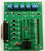
User's Guide
SBOU117A – September 2011 – Revised May 2016
BUF22821EVM-USB Evaluation Board and Software
Tutorial
This user's guide describes the characteristics, operation, and use of the BUF22821EVM-USB evaluation
board. It discusses how to set up and configure the software and hardware and reviews various aspects of
the program operation. Throughout this document, the terms evaluation board, evaluation module, and
EVM are synonymous with the BUF22821EVM-USB. This user's guide also includes information regarding
operating procedures and input/output connections, an electrical schematic, printed circuit board (PCB)
layout drawings, and a parts list for the EVM.
1
2
3
4
5
6
Contents
Overview ..................................................................................................................... 2
BUF22821EVM-USB Hardware Setup .................................................................................... 4
BUF22821EVM-USB Hardware............................................................................................ 6
BUF22821EVM-USB Features ........................................................................................... 12
BUF22821EVM-USB Software Setup ................................................................................... 15
BUF22821EVM-USB Documentation .................................................................................... 26
List of Figures
1
Hardware Included With BUF22821EVM-USB Kit ...................................................................... 3
2
BUF22821EVM-USB Hardware Setup .................................................................................... 4
3
BUF22821EVM-USB Board Block Diagram.............................................................................. 5
4
USB_DIG_Platform Block Diagram
5
Typical Hardware Connections for the BUF22821EVM-USB .......................................................... 7
6
Connecting External Power to the BUF22821EVM-USB ............................................................... 8
7
Connecting the USB Cable to the USB_DIG_Platform ................................................................. 9
8
Confirmation of USB_DIG_Platform Driver Installation ................................................................. 9
9
Default Jumper Locations for BUF22821EVM-USB ................................................................... 10
10
BKSEL Switch .............................................................................................................. 13
11
BUF22821EVM-USB Software Install Window ......................................................................... 15
12
BUF22821EVM-USB Software License Agreements.................................................................. 16
13
BUF22821EVM-USB Software Installation Progress .................................................................. 16
14
BUF22821EVM-USB Software About Button........................................................................... 16
15
BUF22821EVM-USB Software Interface ................................................................................ 17
16
Communication Error with USB_DIG_Platform
17
JMP5 Setting for Logic ‘0’ ................................................................................................. 18
18
JMP5 Setting for Logic ‘1’ ................................................................................................. 19
19
Measuring and Entering Power-Supply Voltage
20
Auto Write Feature Enabled .............................................................................................. 20
21
Save File Prompt ........................................................................................................... 21
22
Saved Data Format ........................................................................................................ 22
.......................................................................................
........................................................................
.......................................................................
6
18
19
PowerPAD is a trademark of Texas Instruments.
Microsoft, Windows are registered trademarks of Microsoft Corporation.
I2C is a trademark of NXP Semiconductors.
WinZIP is a registered trademark of WinZip International LLC.
All other trademarks are the property of their respective owners.
SBOU117A – September 2011 – Revised May 2016
Submit Documentation Feedback
BUF22821EVM-USB Evaluation Board and Software Tutorial
Copyright © 2011–2016, Texas Instruments Incorporated
1
�Overview
1
www.ti.com
23
Load File Prompt ........................................................................................................... 22
24
Run Batch Dialog........................................................................................................... 23
25
Control Panel Window ..................................................................................................... 24
26
Program OTP All Channels ............................................................................................... 25
27
BUF22821EVM-USB Board Schematic ................................................................................. 26
28
BUF22821EVM-USB PCB Top Layer (Component Layout) .......................................................... 27
Overview
The BUF22821 is a programmable gamma-voltage generator and VCOM calibrator. This device offers 22
programmable gamma channels, two programmable VCOM channels, and two static gamma channels,
making it ideal for 10-bit source TFT-LCD reference drivers.
The BUF22821EVM-USB is a platform for evaluating the performance of the BUF22821 under various
signal, reference, and supply conditions. This document gives a general overview of the BUF22821EVMUSB, and provides a general description of the features and functions to be considered while using this
evaluation module.
2
BUF22821EVM-USB Evaluation Board and Software Tutorial
SBOU117A – September 2011 – Revised May 2016
Submit Documentation Feedback
Copyright © 2011–2016, Texas Instruments Incorporated
�Overview
www.ti.com
1.1
BUF22821EVM-USB Kit Contents
Table 1 lists the contents of the BUF22821EVM-USB kit. Figure 1 shows all of the included hardware.
Contact the Texas Instruments Product Information Center nearest you if any component is missing. It is
highly recommended that you also check the BUF22821 product folder on the TI web site at www.ti.com to
verify that you have the latest versions of the related software.
Table 1. BUF22821EVM-USB Kit Contents
Item
Quantity
BUF22821EVM-USB PCB Test Board
1
USB_DIG_Platform PCB
1
USB Cable
1
Barrel plug cable assembly
1
User’s Guide CD-ROM
1
Figure 1. Hardware Included With BUF22821EVM-USB Kit
SBOU117A – September 2011 – Revised May 2016
Submit Documentation Feedback
BUF22821EVM-USB Evaluation Board and Software Tutorial
Copyright © 2011–2016, Texas Instruments Incorporated
3
�Overview
1.2
www.ti.com
Related Documentation from Texas Instruments
The following documents provide information regarding Texas Instruments' integrated circuits used in the
assembly of the BUF22821EVM-USB. This user's guide is available from the TI web site under literature
number SBOU116. Any letter appended to the literature number corresponds to the document revision
that is current at the time of the writing of this document. Newer revisions may be available from the TI
web site, or call the Texas Instruments' Literature Response Center at (800) 477-8924 or the Product
Information Center at (972) 644-5580. When ordering, identify the document by both title and literature
number.
Table 2. Related Documentation
Document
2
Literature Number
BUF22821 Product Data Sheet
SBOS399
USB_DIG_Platform User Guide
SBOU058
BUF22821EVM-USB Hardware Setup
This section discusses the overall system setup for the BUF22821EVM-USB. The PC runs software that
communicates with the USB_DIG_Platform. The USB_DIG_Platform generates the analog and digital
signals used to communicate with the BUF22821 test board. Connectors on the BUF22821 test board
allow the user to connect to the system under various test conditions and monitor the power, current, and
voltage. A block diagram of the overall hardware setup is shown in Figure 2.
+ 6 VDC
Wall Supply
BUF22821
Analog Supply
Measurement
Device
BUF22821EVM-USB
Test Board
Computer
Outputs
USB DIG Platform
Figure 2. BUF22821EVM-USB Hardware Setup
4
BUF22821EVM-USB Evaluation Board and Software Tutorial
SBOU117A – September 2011 – Revised May 2016
Submit Documentation Feedback
Copyright © 2011–2016, Texas Instruments Incorporated
�BUF22821EVM-USB Hardware Setup
www.ti.com
2.1
Theory of Operation for BUF22821 Hardware
Figure 3 shows the BUF22821 test board hardware setup. The functionality of the PCB is such that it
provides connections to the I2C™ and general-purpose inputs/outputs (GPIOs) on the USB_DIG_Platform
board. It also provides connection points for external connections of the shunt voltage, bus voltage, and
ground.
External BUF22821
Analog Power Supply
T1
VDUT Supply
(VSD Power Supply)
25-Pin Male
DSUB
J1
Test Outputs
TP1
BUF22821
Test Point
Header
2
I C Interface
2
I C A0 Address
Jumper
Figure 3. BUF22821EVM-USB Board Block Diagram
2.2
Signal Definitions of J1 (25-Pin Male DSUB)
Table 3 shows the various signals connected to J1 on the BUF22821 test board.
Table 3. J1 Signal Definition for BUF22821EVM-USB
(1)
Pin No on U1
Signal
BUF22821 Pin
1
N/C
No connection
2
N/C
No connection
3
N/C
No connection
4
N/C
No connection
5
N/C
No connection
6
N/C
No connection
7
N/C
No connection
8
N/C
No connection
9
I2C_SCK
No connection
10
I2C_SDA2
No connection
11
N/C
No connection
12
I2C_SCK_ISO
I2C clock signal (SCL) channel 1; can be
disconnected using a switch
13
I2C_SDA_ISO
I2C data signal (SDA) channel 1; can be
disconnected using a switch
14
N/C
No connection
15
N/C
No connection
16
N/C
No connection
17
VDUT
Switched 3-V/5-V power (1)
18
VCC
No connection
19
N/C
No connection
20
N/C
No connection
21
GND
Common ground connection
22
SPI_SCK
No connection
23
SPI_CS1
No connection
24
SPI_DOUT1
No connection
25
SPI_DIN1
No connection
When power is switched off, digital I/O is also switched off.
SBOU117A – September 2011 – Revised May 2016
Submit Documentation Feedback
BUF22821EVM-USB Evaluation Board and Software Tutorial
Copyright © 2011–2016, Texas Instruments Incorporated
5
�BUF22821EVM-USB Hardware
2.2.1
www.ti.com
Theory of Operation for USB_DIG_Platform
Figure 4 shows the block diagram for the USB_DIG_Platform. This platform is a general-purpose data
acquisition system that is used on several different Texas Instruments evaluation modules. The details of
its operation are included in a separate document, SBOU058 (available for download at www.ti.com). The
block diagram shown in Figure 4 gives a brief overview of the platform. The primary control device on the
USB_DIG_Platform is the TUSB3210. The barrel connector cable assembly included in the EVM kit can
be used to connect an external power supply to the USB DIG through J5.
3.3-V
Regulator
V_USB
5V
USB_DIG_Platform
VSmC
3.3V
TUSB3210
8052mC
with USB Interface
and UART
USB
From Computer
Reset Button
and
Power-On Reset
Adjustable
Regulator
Buffers and
Latches
2
I C, SPI
Control Bits and
Measure Bits
Calibration
EEPROM
8K Byte
EEPROM
VCC
(2.7 V to 5.5 V)
Power
Switching
VDUT
(2.7 V to 5.5 V)
Switched Power
External Power
(6 VDC)
Figure 4. USB_DIG_Platform Block Diagram
3
BUF22821EVM-USB Hardware
This section provides details about connecting the two PCBs of the BUF22821EVM-USB together,
applying power, connecting the USB cable, and setting the jumpers.
3.1
Electrostatic Discharge Warning
CAUTION
Many of the components on the BUF22821EVM-USB are susceptible to
damage by electrostatic discharge (ESD). Customers are advised to observe
proper ESD handling precautions when unpacking and handling the EVM,
including the use of a grounded wrist strap at an approved ESD workstation.
6
BUF22821EVM-USB Evaluation Board and Software Tutorial
SBOU117A – September 2011 – Revised May 2016
Submit Documentation Feedback
Copyright © 2011–2016, Texas Instruments Incorporated
�BUF22821EVM-USB Hardware
www.ti.com
3.2
Typical Hardware Connections
Setting up the BUF22821EVM-USB hardware involves connecting the BUF22821 test board and the
USB_DIG_Platform together via a 25-pin DSUB connector and then applying power. The external
connections may be connected to the real-world system that the BUF22821 is to be incorporated into.
Figure 5 shows the typical hardware connections.
Figure 5. Typical Hardware Connections for the BUF22821EVM-USB
3.3
Connecting the Hardware
To connect the BUF22821 Test Board and the USB_DIG_Platform together, gently push on both sides of
the DSUB connectors. Note that the USB_DIG_Platform board has two DSUB connectors; either DSUB
connector may be used. Make sure that the two connectors are completely pushed together; loose
connections may cause intermittent operation.
SBOU117A – September 2011 – Revised May 2016
Submit Documentation Feedback
BUF22821EVM-USB Evaluation Board and Software Tutorial
Copyright © 2011–2016, Texas Instruments Incorporated
7
�BUF22821EVM-USB Hardware
www.ti.com
Connecting Power
After the boards are conjoined, connect the +6-V wall supply to the USB_DIG_Platform board as shown in
Figure 6. Note that it is always necessary to connect the power to the DIG before connecting the USB
cable. If the USB cable is connected before the power, the computer may attempt communication to an
unpowered device that is unable to respond. In addition, the BUF22821 test board requires an external dc
power source. This source is not included with the kit, and its voltage may differ depending on your testing
needs. The source will be used to provide dc supply voltage to the BUF22821 test board.
Figure 6. Connecting External Power to the BUF22821EVM-USB
8
BUF22821EVM-USB Evaluation Board and Software Tutorial
SBOU117A – September 2011 – Revised May 2016
Submit Documentation Feedback
Copyright © 2011–2016, Texas Instruments Incorporated
�BUF22821EVM-USB Hardware
www.ti.com
Connecting the USB Cable to the USB_DIG_Platform
Once power is connected, the USB cable must be connected to the DIG, as shown in Figure 7.
Figure 7. Connecting the USB Cable to the USB_DIG_Platform
Note that the Test Board and USB_DIG_Platform must be powered on before connecting the USB cable.
Typically, the computer responds with a Found New Hardware, USB Device pop-up dialog. The popup
window typically changes to Found New Hardware, USB Human Interface Device. This pop-up window
indicates that the device is ready to be used. The USB_DIG_Platform uses the human interface device
drivers that are part of the Microsoft® Windows® operating system.
In some cases, the Windows Add Hardware wizard is shown. If this prompt appears, allow the system
device manager to install the human interface drivers by clicking Yes when requested to install drivers.
Windows then confirms installation of the drivers with the message shown in Figure 8.
Figure 8. Confirmation of USB_DIG_Platform Driver Installation
SBOU117A – September 2011 – Revised May 2016
Submit Documentation Feedback
BUF22821EVM-USB Evaluation Board and Software Tutorial
Copyright © 2011–2016, Texas Instruments Incorporated
9
�BUF22821EVM-USB Hardware
3.4
www.ti.com
BUF22821EVM-USB Default Jumper Settings
Figure 9 shows the default jumpers configuration for the BUF22821EVM-USB. In general, the jumper
settings of the USB_DIG_Platform do not need to be changed. You may want to change some of the
jumpers on the BUF22821 Test Board to match your specific configuration. For instance, you may wish to
set a specific I2C address.
Figure 9. Default Jumper Locations for BUF22821EVM-USB
10
BUF22821EVM-USB Evaluation Board and Software Tutorial
SBOU117A – September 2011 – Revised May 2016
Submit Documentation Feedback
Copyright © 2011–2016, Texas Instruments Incorporated
�BUF22821EVM-USB Hardware
www.ti.com
Table 4 summarizes the function of the BUF22821 Test Board jumpers. For most application, jumpers 2
through 5 are all set to the default positions.
Table 4. BUF22821 Test Board Jumper Functions
Jumper
Default
JMP1
INT
This jumper selects whether the VSD pin on the
BUF22821 is connected to the VDUT signal
generated from the USB_DIG_Platform or whether
the digital supply pin is connected to terminal T2,
allowing for an external supply to power the digital
circuitry. The default INT position connects the VSD
pin to the VDUT control signal.
JMP2
INT
This jumper selects whether the SCL pin on the
BUF22821 is connected to the I2C_SCK_ISO signal
generated from the USB_DIG_Platform or whether
the SCL pin is connected to terminal T5, allowing
for an external source to control the I2C clock line.
The default INT position connects the SCL pin to
the I2C_SCK_ISO control signal.
JMP3
INT
This jumper selects whether the SDA pin on the
BUF22821 is connected to the I2C_SDA_ISO signal
generated from the USB_DIG_Platform or whether
the SDA pin is connected to terminal T5, allowing
for an external source to control the I2C data line.
The default INT position connects the SDA pin to
the I2C_SDA_ISO control signal.
JMP4
INT
This jumper selects whether the BKSEL pin on the
BUF22821 is controlled by the manual switch
located on the BUF22821 EVM or whether the
BKSEL can be controlled by an external source
connected to terminal T3. The default INT position
allows the BKSEL pin to be controlled by the
manual switch.
JMP5
0
This jumper selects I2C A0 address selection. Two
separate I2C addresses can be selected, depending
on whether JMP6 is set to high or low.
JMP6
No Connection
This jumper selects whether or not the STATIN_H
pin on the BUF22821 is connected to the VS signal
generated by the external analog power supply
input at terminal T1, or whether the STATIN_H pin
is connected to a user-designated reference, which
is set using an external input at terminal T4 as well
as resistors R1 and R2. The default position leaves
the STATIN_H connection open.
JMP7
No Connection
This jumper selects whether or not the STATIN_L
pin on the BUF22821 is connected to ground or
whether the STATIN_L pin is connected to a userdesignated reference, which is set using an external
input at terminal T4 as well as resistors R3 and R4.
The default position leaves the STATIN_L
connection open.
SBOU117A – September 2011 – Revised May 2016
Submit Documentation Feedback
Purpose/Description
BUF22821EVM-USB Evaluation Board and Software Tutorial
Copyright © 2011–2016, Texas Instruments Incorporated
11
�BUF22821EVM-USB Features
www.ti.com
Table 5 summarizes the function of the USB_DIG_Platform jumpers. For most applications, the default
positions should be used. A separate document (SBOU058) provides details regarding the operation and
design of the USB_DIG_Platform.
Table 5. USB_DIG_Platform Jumper Functions
(1)
4
Jumper
Default
Purpose/Description
JUMP1
EXT
This jumper selects external power or bus power.
External power is applied on J5 or T3 (up to +9 V
DC). Bus power is +5 V from the USB. External
power is typically used because the USB bus power
introduces additional noise.
JUMP2
EXT
Same as JUMP1.
JUMP3
EE ON
JUMP4, JUMP5
L, L
This jumper sets the address for the
USB_DIG_Platform board. The only reason to
change from the default is if multiple boards are
being used.
JUMP9
5V
This jumper selects the voltage of the device under
test supply (VDUT = 5 V or 3 V). This jumper is
typically the only jumper that changes for most
applications.
JUMP10
WP ON
This write protects the firmware EEPROM.
JUMP11
WP ON
This write protects the calibration EEPROM.
JUMP13
REG
JUMP14
9V
JUMP17
BUS
While in the BUS position, VDUT operation is normal.
While in the VRAW position, the VDUT supply is
connected to an external source. This configuration
allows for any value of VDUT between 3 V and 5 V. (1)
JUMP18
VDUT
Connects the pull-up on GPIO to the VDUT supply or
the VCC supply.
This jumper determines where the TUSB3210 loads
the USB_DIG_Platform firmware upon power-up or
reset. The EE Off position is used for development
or firmware update.
Uses the regulator output to generate the VDUT
supply. The USB bus can be used as the VDUT
supply.
Uses the external power (9 V as opposed to the
bus)
Adjusting beyond this range damages the EVM.
BUF22821EVM-USB Features
This section describes some of the hardware features present on the BUF22821 Test Board.
JMP1: VSD Control Setting
Jumper JMP1 selects where the BUF22821 digital supply pin is connected. If JMP1 is set to the INT
position, the DVDD pin is connected to the switchable VDUT signal generated from the USB_DIG_Platform.
This voltage can be set to either +3.3 V or +5 V, depending on how JUMP9 on the USB_DIG_Platform is
set. While JMP1 is set to the INT position, the VSD Power button on the BUF22821 software is able to
control whether the VDUT supply voltage is turned on or off.
When JMP1 is set in the EXT position, an external supply connected to terminal T2 can be used to
provide the digital supply voltage for the BUF22821.
12
BUF22821EVM-USB Evaluation Board and Software Tutorial
SBOU117A – September 2011 – Revised May 2016
Submit Documentation Feedback
Copyright © 2011–2016, Texas Instruments Incorporated
�BUF22821EVM-USB Features
www.ti.com
JMP2: I2C SCL Control Setting
Jumper JMP2 selects where the BUF22821 I2C SCL pin is connected. If JMP2 is set to the INT position,
the I2C clock signal is generated from the I2C_SCK_ISO signal from the USB_DIG_Platform.
When JMP2 is set in the EXT position, an external source connected to SCL pin of terminal T5 can be
used to provide the I2C SCK signal to the BUF22821.
JMP3: I2C SDA Control Setting
Jumper JMP3 selects where the BUF22821 I2C SDA pin is connected. If JMP3 is set to the INT position,
the I2C data signal is generated from the I2C_SDA_ISO signal from the USB_DIG_Platform.
When JMP3 is set in the EXT position, an external source connected to SDA pin of terminal T5 can be
used to provide the I2C SDA signal for the BUF22821.
4.1
JMP4: BKSEL Control Setting
Jumper JMP4 determines how the OTP memory bank selection is controlled. There are two settings for
JMP4: position INT and position EXT. Position INT specifies that control of the BKSEL pin is handled on
the BUF22821 Test Board. For this jumper setting, the BKSEL switch controls whether the Bank0 or
Bank1 OTP is selected (as shown in Figure 10).
When JMP4 is set to the EXT position, an external control signal connected to terminal T3 determines the
selection of which OTP bank to be used.
Figure 10. BKSEL Switch
4.2
JMP5: I2C Address Hardware Setting
Jumper JMP5 sets the hardware configuration for the A0 I2C address pin on the BUF22821. Using JMP5,
the A0 address can be set to either a logic '1' or a logic '0' to allow for two unique I2C addresses. See
Section 5.0.1 on how to configure the BUF22821EVM-USB software to match the JMP5 hardware setting.
SBOU117A – September 2011 – Revised May 2016
Submit Documentation Feedback
BUF22821EVM-USB Evaluation Board and Software Tutorial
Copyright © 2011–2016, Texas Instruments Incorporated
13
�BUF22821EVM-USB Features
www.ti.com
JMP6: STATIN_H Control Setting
Jumper JMP6 is selects where the BUF22821 high reference supply pin STATIN_H is connected. If JMP6
is set to the INT position, STATIN_H is connected to VS, the external analog supply input at terminal T1.
When JMP6 is set to the EXT position, the reference voltage is then designated by the user with the
STATIN_H pin of terminal T4, along with resistors R1 and R2. An external power supply is connected to
the STATIN_H pin of terminal T4, and R1 and R2 act as a voltage-divider circuit; the user sets the values
of R1 and R2 to achieve the desired reference voltage using Equation 1:
R2
STATIN_L = VSUP_H
R1 + R2
(1)
(
(
Where VSUP_H is the input supply voltage seen at the STATIN_H pin of terminal T4.
JMP7: STATIN_L Control Setting
Jumper JMP7 is selects where the BUF22821 high reference supply pin STATIN_L is connected. If JMP8
is set to the INT position, STATIN_L is connected to ground.
When JMP7 is set to the EXT position, the reference voltage is then designated by the user with the
STATIN_L pin of terminal T4, along with resistors R3 and R4. An external power supply is connected to
the STATIN_L pin of terminal T4, and R3 and R4 act as a voltage-divider circuit; the user sets the values
of R3 and R4 to achieve the desired reference voltage using Equation 2:
R4
STATIN_L = VSUP_L
R3 + R4
(2)
(
(
Where VSUP_L is the input supply voltage seen at the STATIN_L pin of terminal T4.
BUF22821 Device Placement
The BUF22821EVM-USB provides two separate locations on the board where the BUF22821 test device
can be installed.
Location U1 allows for a BUF22821 device that is soldered down on a DIP adaptor board to be installed
on the BUF22821 Test Board. The output capability of the BUF22821 that is soldered on this adaptor
board can be fully evaluated. The PowerPAD™ of this soldered BUF22821 is connected correctly and
allows the device to dissipate the necessary power while being evaluated.
Location U2 on the BUF22821 Test Board is a 24-pin, QFN-package test socket that allows the user to
evaluate and program many devices very quickly. One drawback to this socket is that there is no
connection to the PowerPAD of the BUF22821. Because of this limitation, while the device is placed in this
socket, it cannot be operated to its full output capability as a result of thermal dissipation limitations.
CAUTION
Only one location should be populated at a time. The use of both locations
simultaneously will likely damage one or both of the devices under test.
Terminal Strip TP1
Terminal strip TP1 provides the individual output signals on a single row of headers as well as a row of
vias. This footprint offers the user multiple options to interface the output signals of the BUF22821 with an
available display panel (provided by the user). The user can also develop a custom cable to connect the
headers to this panel directly, or to solder the headers directly to the individual vias.
14
BUF22821EVM-USB Evaluation Board and Software Tutorial
SBOU117A – September 2011 – Revised May 2016
Submit Documentation Feedback
Copyright © 2011–2016, Texas Instruments Incorporated
�BUF22821EVM-USB Software Setup
www.ti.com
5
BUF22821EVM-USB Software Setup
This section discusses how to install the BUF22821EVM-USB software.
BUF22821EVM-USB Software Operating Systems
The BUF22821EVM-USB software has been tested on Microsoft Windows XP, Vista, and Windows7
operating systems (OS) with United States and European regional settings. The software should also
function on other Windows OS platforms.
BUF22821 Software Installation
The BUF22821EVM-USB software is included on the CD that is shipped with the EVM kit. It is also
available through the BUF22821EVM-USB product folder on the TI web site. To download the software to
your system, insert the disc into an available CD-ROM drive. Navigate to the drive contents and open the
BUF22821EVM-USB software folder. Locate the compressed file (BUF22821EVM-USB.zip) and open it.
Using WinZIP®® or a similar file compression program; extract the BUF22821EVM-USB files into a
specific BUF22821EVM-USB folder (for example, C:\BUF22821EVM-USB) on your hard drive.
Once the files are extracted, navigate to the BUF22821EVM-USB folder you created on your hard drive.
Locate the setup.exe file and execute it to start the installation. The BUF22821 software installer file then
opens to begin the installation process, as shown in Figure 11.
Figure 11. BUF22821EVM-USB Software Install Window
SBOU117A – September 2011 – Revised May 2016
Submit Documentation Feedback
BUF22821EVM-USB Evaluation Board and Software Tutorial
Copyright © 2011–2016, Texas Instruments Incorporated
15
�BUF22821EVM-USB Software Setup
www.ti.com
After the installation process initializes, the user is given the choice of selecting the directory to install the
program. Generally, defaulting to C:\Program Files\BUF22821\ and C:\Program Files\National Instruments\
is an acceptable choice. Following this option, two license agreements are presented that must be
accepted as shown in Figure 12.
Figure 12. BUF22821EVM-USB Software License Agreements
After accepting the Texas Instruments and National Instruments license agreements, the progress bar
opens and shows the installation of the software, as Figure 13 illustrates. Once the installation process is
completed, click Finish.
Figure 13. BUF22821EVM-USB Software Installation Progress
Software Description and Set-Up
The BUF22821EVM-USB software allows the user to read and write to all registers in the BUF22821
gamma correction buffer. Furthermore, it allows programming of the OTP register on the BUF22821. The
software also permits the user to select either I2C address. Press the About button to verify that you have
the latest version of the software; the contents of this window are shown in Figure 14 .
Figure 14. BUF22821EVM-USB Software About Button
16
BUF22821EVM-USB Evaluation Board and Software Tutorial
SBOU117A – September 2011 – Revised May 2016
Submit Documentation Feedback
Copyright © 2011–2016, Texas Instruments Incorporated
�BUF22821EVM-USB Software Setup
www.ti.com
BUF22821EVM-USB Software Overview
This section discusses how to use the BUF22821EVM-USB software.
Starting the BUF22821EVM-USB Software
The BUF22821EVM-USB software can be operated through the Start menu in Windows. From the Start
menu, select All Programs, and then select the BUF22821EVM-USB program to start the software.
Figure 15 shows how the software should appear if the BUF22821EVM-USB is functioning properly.
Figure 15. BUF22821EVM-USB Software Interface
SBOU117A – September 2011 – Revised May 2016
Submit Documentation Feedback
BUF22821EVM-USB Evaluation Board and Software Tutorial
Copyright © 2011–2016, Texas Instruments Incorporated
17
�BUF22821EVM-USB Software Setup
www.ti.com
Figure 16 shows an error that pops up if the computer cannot communicate with the EVM. If you receive
this error, first ensure that the USB cable is properly connected on both ends. This error can also occur if
you connect the USB cable before the USB_DIG_Platform power source. Another possible cause for this
error is a problem with the USB Human Interface Device Driver on the computer you are using. Make sure
that the device is recognized when the USB cable is plugged in; this action is indicated by a Windowsgenerated confirmation sound.
Figure 16. Communication Error with USB_DIG_Platform
Using the BUF22821 Software
5.0.1
I2C Address Selection
As mentioned previously (refer to Section 4.2), jumper JMP5 is used to set the I2C address pin of the
BUF22821. Figure 17 shows how the hardware and software must both be set to enable communication
between the BUF22821EVM-USB and the software. Without jumper JMP5 and the software address
button configured correctly, the software cannot communicate with the BUF22821 device.
Figure 17. JMP5 Setting for Logic ‘0’
18
BUF22821EVM-USB Evaluation Board and Software Tutorial
SBOU117A – September 2011 – Revised May 2016
Submit Documentation Feedback
Copyright © 2011–2016, Texas Instruments Incorporated
�BUF22821EVM-USB Software Setup
www.ti.com
When JMP5 and the software are set as shown in Figure 18, the second I2C address can be configured.
Figure 18. JMP5 Setting for Logic ‘1’
Measuring the Power Supply
You must measure the power supply (VS) with respect to the GND on the BUF22821 Test Board and enter
it in the Vsup field located in the top section of the software interface as shown in Figure 19.
Figure 19. Measuring and Entering Power-Supply Voltage
The voltage out of each digital-to-analog converter (DAC) is calculated according to the VS value entered.
Changing the value in the channel 6 cell as shown below, for instance, immediately changes the output of
channel 6 to 0.996 V. The calculation is performed according to Equation 3.
VDAC_CHANNEL = VS x Code_in_decimal
1024
(3)
SBOU117A – September 2011 – Revised May 2016
Submit Documentation Feedback
BUF22821EVM-USB Evaluation Board and Software Tutorial
Copyright © 2011–2016, Texas Instruments Incorporated
19
�BUF22821EVM-USB Software Setup
www.ti.com
For example:
Channel 6: Code 44 (hexadecimal) = 68 (decimal)
VDAC_CHANNEL = 15 V x 68 = 0.996 V
1024
(4)
Read DAC Button
By pressing the Read DAC button in the BUF22821EVM-USB software, all of the BUF22821 DAC
registers are read to obtain the respective current register contents. Once the read procedure is complete,
all of the corresponding text boxes are updated to show the current values present in the DAC registers.
Write DAC Button
The method used to write the values in the DAC registers is based on whether or not the Auto Write
feature is enabled. The BUF22821 has two methods of writing information into the DAC registers. The first
method allows for the output voltage to change immediately after the writing to the DAC register. In the
BUF22821EVM-USB software, this mode is configured by enabling the Auto Write feature found in the
Buffer Menu drop-down menu. In this mode, as an individual channel is written to, the output voltage
changes as soon as the user moves to a different text box in the software.
The second method of writing to the DAC registers allows for the user to write multiple channels and then
have all of the output voltages change at the same time, rather than each channel voltage changing as
soon as it is written to. Disabling the Auto Write feature in the software allows the user to enter all of the
desired values for all of the channels, and then press the Write DAC button to change all of the output
voltage of all of the channels at one time. When the Auto Write feature is enabled, no change occurs to
the output voltages when the Write DAC button is pressed. This action occurs because after the text box
for a given channel has been updated, as soon as another item in the software is clicked, the Auto Write
feature automatically performs a write command to the updated channel that then updates the output
voltage. When in the Auto Write enabled mode, the Write DAC button cannot be pressed with data in the
corresponding channel text boxes that are different than the values already stored in the DAC register; no
change to the DAC registers will occur. Figure 20 shows the location in the Buffer Menu with the Auto
Write feature enabled. Click the Auto Write feature again to enable/disable the feature, depending upon its
current state.
Figure 20. Auto Write Feature Enabled
20
BUF22821EVM-USB Evaluation Board and Software Tutorial
SBOU117A – September 2011 – Revised May 2016
Submit Documentation Feedback
Copyright © 2011–2016, Texas Instruments Incorporated
�BUF22821EVM-USB Software Setup
www.ti.com
Reset Button
Pressing the Reset button in the BUF22821EVM-USB software performs two functions. First, a GeneralCall Reset for the BUF22821 is performed. The status of the DAC registers after this General-Call Reset
default to 1000000000, or mid-supply. The second function performed after the Reset button is pressed is
that a Read DAC call is made to update the corresponding channel text boxes to the current value for
each channel.
Save to File Button
The register configurations of the BUF22821 DACs are displayed in both analog voltage and in
hexadecimal (refer to Figure 15). The DAC codes (that is, gamma voltages) can also be saved to a text
file (.txt) using the Save to File button.
Pressing the Save to File button opens a file-save dialog box similar to that shown in Figure 21. Pressing
the folder icon creates a new folder on your PC. It is a good idea to create a directory exclusively for
BUF22821 DAC code (gamma voltage) files. Enter a unique file name in the File name field to store your
BUF22821 register information. Press the OK button to save the file.
Figure 21. Save File Prompt
SBOU117A – September 2011 – Revised May 2016
Submit Documentation Feedback
BUF22821EVM-USB Evaluation Board and Software Tutorial
Copyright © 2011–2016, Texas Instruments Incorporated
21
�BUF22821EVM-USB Software Setup
www.ti.com
Saving the BUF22821 DAC codes (gamma voltages) creates a text file that can be opened in a text editor,
as illustrated in Figure 22.
Figure 22. Saved Data Format
Load From File Button
The BUF22821EVM-USB software is also able to load data saved from previous evaluations. A saved
register configuration can be loaded into the BUF22821 using the Load From File button, shown in
Figure 23. The program recalls where you saved the last register configuration. Simply select the desired
configuration and press Open.
Figure 23. Load File Prompt
22
BUF22821EVM-USB Evaluation Board and Software Tutorial
SBOU117A – September 2011 – Revised May 2016
Submit Documentation Feedback
Copyright © 2011–2016, Texas Instruments Incorporated
�BUF22821EVM-USB Software Setup
www.ti.com
Changing DAC Analog Voltage
The voltage of any of the DAC channels can be adjusted in several ways. One way is to change the
voltage by entering the desired voltage directly in the voltage text box. In order to be able to manually type
the voltage into the text box, first click on the cell to be edited. Click a second time and the cell turns from
blue to black and allows the updated voltage to be typed in the cell. The hexadecimal DAC codes can be
entered in the Code column in the same manner.
Another method of changing the voltage of a DAC channel is through the use of the slider on the main
software window (refer to Figure 15). There is only a single slider that is used for all channels. In order to
use the slider to adjust the voltage of a particular channel, the channel must first be selected. Clicking on
either the channel number, voltage, or code of a particular channel highlights the entire channel row and
makes it blue to indicate which channel is selected. Adjusting the slider bar then only updates the
highlighted channel.
The final method to change the DAC voltages is through the ±1 Code and ±5 Code buttons on the main
software window. These buttons allow for fine and coarse adjustments to the highlighted channel to allow
the user to quickly step the channel output up or down as needed, without having to manually enter the
changes in the Code column.
Run Batch Button
The Run Batch button (as indicated in Figure 24) enables the user to configure the BUF22821 to cycle
through different register configurations in a continuous loop. When connected to the end application, this
feature can be used to cycle through different gamma settings to determine what the optimal settings must
be for a given application.
Figure 24. Run Batch Dialog
When the Run Batch button is pressed, a new dialog box displays as Figure 24 shows. The delay time is
the amount of time between loading new configurations into the BUF22821.
Use the Single Step Up and Single Step Down buttons to step through the selected files manually. The
currently-selected file name is displayed in the lower left corner area of the dialog box. Double-click on the
file names to select them. Once the names have been selected, the check box turns dark. Double-click on
the file name again to unselect it from the batch run. In Figure 24, two configuration files are selected.
SBOU117A – September 2011 – Revised May 2016
Submit Documentation Feedback
BUF22821EVM-USB Evaluation Board and Software Tutorial
Copyright © 2011–2016, Texas Instruments Incorporated
23
�BUF22821EVM-USB Software Setup
www.ti.com
Control Panel Button
Pressing the Control Panel button brings up a display panel that allows you to adjust each channel using
a set of graphical sliders, as shown in Figure 25. Simply drag the slider to adjust the desired channel
output. The DAC code and corresponding output value of each channel changes automatically. This action
is similar to the slider present on the main BUF22821EVM-USB software window that changes based on
the channel that is highlighted.
Figure 25. Control Panel Window
24
BUF22821EVM-USB Evaluation Board and Software Tutorial
SBOU117A – September 2011 – Revised May 2016
Submit Documentation Feedback
Copyright © 2011–2016, Texas Instruments Incorporated
�BUF22821EVM-USB Software Setup
www.ti.com
Program OTP All Channels Button
As Figure 26 shows, pressing the Program OTP All Channels button allows you to program a gamma
curve into the nonvolatile memory in the BUF22821. All 22 channels (including the VCOM channels) are
then programmed simultaneously. The values are stored in the memory bank that is selected via the
BKSEL switch (see Section 4.1).
Figure 26. Program OTP All Channels
SBOU117A – September 2011 – Revised May 2016
Submit Documentation Feedback
BUF22821EVM-USB Evaluation Board and Software Tutorial
Copyright © 2011–2016, Texas Instruments Incorporated
25
�BUF22821EVM-USB Documentation
6
www.ti.com
BUF22821EVM-USB Documentation
This section contains the complete bill of materials and PCB layout for the BUF22821EVM-USB.
NOTE: These board layouts are not to scale. These image are intended to show how the board is
laid out; they are not intended to be used for manufacturing BUF22821EVM-USB PCBs.
BUF22821EVM-USB Board Schematic
Figure 27 shows the schematic for the BUF22821EVM-USB board.
Figure 27. BUF22821EVM-USB Board Schematic
26
BUF22821EVM-USB Evaluation Board and Software Tutorial
SBOU117A – September 2011 – Revised May 2016
Submit Documentation Feedback
Copyright © 2011–2016, Texas Instruments Incorporated
�BUF22821EVM-USB Documentation
www.ti.com
6.1
PCB Layout
Figure 28 shows the PCB layout of the BUF22821EVM-USB.
Figure 28. BUF22821EVM-USB PCB Top Layer (Component Layout)
SBOU117A – September 2011 – Revised May 2016
Submit Documentation Feedback
BUF22821EVM-USB Evaluation Board and Software Tutorial
Copyright © 2011–2016, Texas Instruments Incorporated
27
�BUF22821EVM-USB Documentation
6.2
www.ti.com
Bill of Materials
Table 6 lists the bill of materials for the BUF22821EVM-USB.
Table 6. BUF22821EVM-USB Test Board Bill of Materials
Item
No.
Qty
Value
Ref Des
1
4
Various
R1 to R4
2
1
249 kΩ
R5
3
2
4.7 μF
4
2
5
Description
Vendor/Mfr
Part Number
Resistor, 1/16W 5% 0603 SMD
Susumu Co Ltd
Various
Resistor, 249 kΩ, 1/16W 5% 0603
SMD
Susumu Co Ltd
RR0816P-2493-D-39D
C1, C2
Capacitor, tantalum, 4.7 μF 35 V
10% SMD
Vishay/Sprague
293D475X9035C2TE3
1 μF
C3, C4
Capacitor, ceramic, 1 μF 25 V Y5V
0603
Murata Electronics North
America
GRM188F51E105ZA12D
8
0.1 μF
C5 to C12
Capacitor ceramic, 0.1 μF 25 V
Y5V 0603
Kemet
C0603C104Z3VACTU
6
1
—
U1
Connector, Rcpt .100 in, 19-Pos
Gold T/H
Samtec
SS-119-G-2
7
2
—
U2
Socket, TSSOP 28-Pin ZIF
ENPLAS
OTS-38(44)-0.5-01
8
1
—
U3
IC Buffer, Schmitt Trigger, SOT235 Texas Instruments
SN74LVC1G17DBVR
9
1
DSUB25
J1
Connector, D-SUB Plug R/A 25Pos 30 Gold (with threaded inserts
and board locks)
AMP/Tyco Electronics
5747842-4
10
4
—
T1 to T4
Terminal block 5 MM 2 Pos
On-Shore Technology
Inc
ED300/2
11
1
—
T5
Terminal block 5 MM 3 Pos
On-Shore Technology
Inc
ED300/3
12
1
—
TP1
Connector, Header 26-Pos .100
in., SGL Gold
Samtec
TSW-126-07-G-S
13
7
—
All Test Points
(VS, VSD, SCL,
SDA, BKSEL,
GNDx2)
Connector, Header 1-Pos .100 in.,
SGL Gold
Samtec
TSW-101-07-G-S
14
4
Standoff
None
Standoffs, Hex , 4-40 Threaded,
0.500 in., length, 0.250 in. OD,
Aluminum Iridite Finish
Keystone
2203
15
4
Screw
None
Screw Machine Phillips, 4-40X1/4
SS
B & F Fastener Supply
PMSSS 440 0025 PH
16
1
SW1
SW1
Switch Toggle SPDT .4 VA PC
MNT
E-Switch
200AWMSP1T1A1M2RE
17
7
Strip cut to
size
(length is 3
pos.)
JMP1 to JMP7
Connector, Header 3-Pos .100 in.,
SGL Gold
Samtec
TSW-103-07-G-S
18
7
Jumper
JMP1 to JMP7
Shunt LP w/Handle 2-Pos 30AU
AMP/Tyco Electronics
881545-2
Revision History
NOTE: Page numbers for previous revisions may differ from page numbers in the current version.
Changes from Original (September 2011) to A Revision ............................................................................................... Page
•
•
•
28
Added new part to the BUF22821EVM-USB Kit Contents table. ................................................................... 3
Changed 'Hardware Included' image. .................................................................................................. 3
Added new language to the first paragraph of the Theory of Operation for USB_DIG_Platform section. ..................... 6
Revision History
SBOU117A – September 2011 – Revised May 2016
Submit Documentation Feedback
Copyright © 2011–2016, Texas Instruments Incorporated
�STANDARD TERMS AND CONDITIONS FOR EVALUATION MODULES
1.
Delivery: TI delivers TI evaluation boards, kits, or modules, including any accompanying demonstration software, components, or
documentation (collectively, an “EVM” or “EVMs”) to the User (“User”) in accordance with the terms and conditions set forth herein.
Acceptance of the EVM is expressly subject to the following terms and conditions.
1.1 EVMs are intended solely for product or software developers for use in a research and development setting to facilitate feasibility
evaluation, experimentation, or scientific analysis of TI semiconductors products. EVMs have no direct function and are not
finished products. EVMs shall not be directly or indirectly assembled as a part or subassembly in any finished product. For
clarification, any software or software tools provided with the EVM (“Software”) shall not be subject to the terms and conditions
set forth herein but rather shall be subject to the applicable terms and conditions that accompany such Software
1.2 EVMs are not intended for consumer or household use. EVMs may not be sold, sublicensed, leased, rented, loaned, assigned,
or otherwise distributed for commercial purposes by Users, in whole or in part, or used in any finished product or production
system.
2
Limited Warranty and Related Remedies/Disclaimers:
2.1 These terms and conditions do not apply to Software. The warranty, if any, for Software is covered in the applicable Software
License Agreement.
2.2 TI warrants that the TI EVM will conform to TI's published specifications for ninety (90) days after the date TI delivers such EVM
to User. Notwithstanding the foregoing, TI shall not be liable for any defects that are caused by neglect, misuse or mistreatment
by an entity other than TI, including improper installation or testing, or for any EVMs that have been altered or modified in any
way by an entity other than TI. Moreover, TI shall not be liable for any defects that result from User's design, specifications or
instructions for such EVMs. Testing and other quality control techniques are used to the extent TI deems necessary or as
mandated by government requirements. TI does not test all parameters of each EVM.
2.3 If any EVM fails to conform to the warranty set forth above, TI's sole liability shall be at its option to repair or replace such EVM,
or credit User's account for such EVM. TI's liability under this warranty shall be limited to EVMs that are returned during the
warranty period to the address designated by TI and that are determined by TI not to conform to such warranty. If TI elects to
repair or replace such EVM, TI shall have a reasonable time to repair such EVM or provide replacements. Repaired EVMs shall
be warranted for the remainder of the original warranty period. Replaced EVMs shall be warranted for a new full ninety (90) day
warranty period.
3
Regulatory Notices:
3.1 United States
3.1.1
Notice applicable to EVMs not FCC-Approved:
This kit is designed to allow product developers to evaluate electronic components, circuitry, or software associated with the kit
to determine whether to incorporate such items in a finished product and software developers to write software applications for
use with the end product. This kit is not a finished product and when assembled may not be resold or otherwise marketed unless
all required FCC equipment authorizations are first obtained. Operation is subject to the condition that this product not cause
harmful interference to licensed radio stations and that this product accept harmful interference. Unless the assembled kit is
designed to operate under part 15, part 18 or part 95 of this chapter, the operator of the kit must operate under the authority of
an FCC license holder or must secure an experimental authorization under part 5 of this chapter.
3.1.2
For EVMs annotated as FCC – FEDERAL COMMUNICATIONS COMMISSION Part 15 Compliant:
CAUTION
This device complies with part 15 of the FCC Rules. Operation is subject to the following two conditions: (1) This device may not
cause harmful interference, and (2) this device must accept any interference received, including interference that may cause
undesired operation.
Changes or modifications not expressly approved by the party responsible for compliance could void the user's authority to
operate the equipment.
FCC Interference Statement for Class A EVM devices
NOTE: This equipment has been tested and found to comply with the limits for a Class A digital device, pursuant to part 15 of
the FCC Rules. These limits are designed to provide reasonable protection against harmful interference when the equipment is
operated in a commercial environment. This equipment generates, uses, and can radiate radio frequency energy and, if not
installed and used in accordance with the instruction manual, may cause harmful interference to radio communications.
Operation of this equipment in a residential area is likely to cause harmful interference in which case the user will be required to
correct the interference at his own expense.
SPACER
SPACER
SPACER
SPACER
SPACER
SPACER
SPACER
SPACER
�FCC Interference Statement for Class B EVM devices
NOTE: This equipment has been tested and found to comply with the limits for a Class B digital device, pursuant to part 15 of
the FCC Rules. These limits are designed to provide reasonable protection against harmful interference in a residential
installation. This equipment generates, uses and can radiate radio frequency energy and, if not installed and used in accordance
with the instructions, may cause harmful interference to radio communications. However, there is no guarantee that interference
will not occur in a particular installation. If this equipment does cause harmful interference to radio or television reception, which
can be determined by turning the equipment off and on, the user is encouraged to try to correct the interference by one or more
of the following measures:
•
•
•
•
Reorient or relocate the receiving antenna.
Increase the separation between the equipment and receiver.
Connect the equipment into an outlet on a circuit different from that to which the receiver is connected.
Consult the dealer or an experienced radio/TV technician for help.
3.2 Canada
3.2.1
For EVMs issued with an Industry Canada Certificate of Conformance to RSS-210
Concerning EVMs Including Radio Transmitters:
This device complies with Industry Canada license-exempt RSS standard(s). Operation is subject to the following two conditions:
(1) this device may not cause interference, and (2) this device must accept any interference, including interference that may
cause undesired operation of the device.
Concernant les EVMs avec appareils radio:
Le présent appareil est conforme aux CNR d'Industrie Canada applicables aux appareils radio exempts de licence. L'exploitation
est autorisée aux deux conditions suivantes: (1) l'appareil ne doit pas produire de brouillage, et (2) l'utilisateur de l'appareil doit
accepter tout brouillage radioélectrique subi, même si le brouillage est susceptible d'en compromettre le fonctionnement.
Concerning EVMs Including Detachable Antennas:
Under Industry Canada regulations, this radio transmitter may only operate using an antenna of a type and maximum (or lesser)
gain approved for the transmitter by Industry Canada. To reduce potential radio interference to other users, the antenna type
and its gain should be so chosen that the equivalent isotropically radiated power (e.i.r.p.) is not more than that necessary for
successful communication. This radio transmitter has been approved by Industry Canada to operate with the antenna types
listed in the user guide with the maximum permissible gain and required antenna impedance for each antenna type indicated.
Antenna types not included in this list, having a gain greater than the maximum gain indicated for that type, are strictly prohibited
for use with this device.
Concernant les EVMs avec antennes détachables
Conformément à la réglementation d'Industrie Canada, le présent émetteur radio peut fonctionner avec une antenne d'un type et
d'un gain maximal (ou inférieur) approuvé pour l'émetteur par Industrie Canada. Dans le but de réduire les risques de brouillage
radioélectrique à l'intention des autres utilisateurs, il faut choisir le type d'antenne et son gain de sorte que la puissance isotrope
rayonnée équivalente (p.i.r.e.) ne dépasse pas l'intensité nécessaire à l'établissement d'une communication satisfaisante. Le
présent émetteur radio a été approuvé par Industrie Canada pour fonctionner avec les types d'antenne énumérés dans le
manuel d’usage et ayant un gain admissible maximal et l'impédance requise pour chaque type d'antenne. Les types d'antenne
non inclus dans cette liste, ou dont le gain est supérieur au gain maximal indiqué, sont strictement interdits pour l'exploitation de
l'émetteur
3.3 Japan
3.3.1
Notice for EVMs delivered in Japan: Please see http://www.tij.co.jp/lsds/ti_ja/general/eStore/notice_01.page 日本国内に
輸入される評価用キット、ボードについては、次のところをご覧ください。
http://www.tij.co.jp/lsds/ti_ja/general/eStore/notice_01.page
3.3.2
Notice for Users of EVMs Considered “Radio Frequency Products” in Japan: EVMs entering Japan may not be certified
by TI as conforming to Technical Regulations of Radio Law of Japan.
If User uses EVMs in Japan, not certified to Technical Regulations of Radio Law of Japan, User is required by Radio Law of
Japan to follow the instructions below with respect to EVMs:
1.
2.
3.
Use EVMs in a shielded room or any other test facility as defined in the notification #173 issued by Ministry of Internal
Affairs and Communications on March 28, 2006, based on Sub-section 1.1 of Article 6 of the Ministry’s Rule for
Enforcement of Radio Law of Japan,
Use EVMs only after User obtains the license of Test Radio Station as provided in Radio Law of Japan with respect to
EVMs, or
Use of EVMs only after User obtains the Technical Regulations Conformity Certification as provided in Radio Law of Japan
with respect to EVMs. Also, do not transfer EVMs, unless User gives the same notice above to the transferee. Please note
that if User does not follow the instructions above, User will be subject to penalties of Radio Law of Japan.
SPACER
SPACER
SPACER
SPACER
SPACER
�【無線電波を送信する製品の開発キットをお使いになる際の注意事項】 開発キットの中には技術基準適合証明を受けて
いないものがあります。 技術適合証明を受けていないもののご使用に際しては、電波法遵守のため、以下のいずれかの
措置を取っていただく必要がありますのでご注意ください。
1.
2.
3.
電波法施行規則第6条第1項第1号に基づく平成18年3月28日総務省告示第173号で定められた電波暗室等の試験設備でご使用
いただく。
実験局の免許を取得後ご使用いただく。
技術基準適合証明を取得後ご使用いただく。
なお、本製品は、上記の「ご使用にあたっての注意」を譲渡先、移転先に通知しない限り、譲渡、移転できないものとします。
上記を遵守頂けない場合は、電波法の罰則が適用される可能性があることをご留意ください。 日本テキサス・イ
ンスツルメンツ株式会社
東京都新宿区西新宿6丁目24番1号
西新宿三井ビル
3.3.3
Notice for EVMs for Power Line Communication: Please see http://www.tij.co.jp/lsds/ti_ja/general/eStore/notice_02.page
電力線搬送波通信についての開発キットをお使いになる際の注意事項については、次のところをご覧くださ
い。http://www.tij.co.jp/lsds/ti_ja/general/eStore/notice_02.page
SPACER
4
EVM Use Restrictions and Warnings:
4.1 EVMS ARE NOT FOR USE IN FUNCTIONAL SAFETY AND/OR SAFETY CRITICAL EVALUATIONS, INCLUDING BUT NOT
LIMITED TO EVALUATIONS OF LIFE SUPPORT APPLICATIONS.
4.2 User must read and apply the user guide and other available documentation provided by TI regarding the EVM prior to handling
or using the EVM, including without limitation any warning or restriction notices. The notices contain important safety information
related to, for example, temperatures and voltages.
4.3 Safety-Related Warnings and Restrictions:
4.3.1
User shall operate the EVM within TI’s recommended specifications and environmental considerations stated in the user
guide, other available documentation provided by TI, and any other applicable requirements and employ reasonable and
customary safeguards. Exceeding the specified performance ratings and specifications (including but not limited to input
and output voltage, current, power, and environmental ranges) for the EVM may cause personal injury or death, or
property damage. If there are questions concerning performance ratings and specifications, User should contact a TI
field representative prior to connecting interface electronics including input power and intended loads. Any loads applied
outside of the specified output range may also result in unintended and/or inaccurate operation and/or possible
permanent damage to the EVM and/or interface electronics. Please consult the EVM user guide prior to connecting any
load to the EVM output. If there is uncertainty as to the load specification, please contact a TI field representative.
During normal operation, even with the inputs and outputs kept within the specified allowable ranges, some circuit
components may have elevated case temperatures. These components include but are not limited to linear regulators,
switching transistors, pass transistors, current sense resistors, and heat sinks, which can be identified using the
information in the associated documentation. When working with the EVM, please be aware that the EVM may become
very warm.
4.3.2
EVMs are intended solely for use by technically qualified, professional electronics experts who are familiar with the
dangers and application risks associated with handling electrical mechanical components, systems, and subsystems.
User assumes all responsibility and liability for proper and safe handling and use of the EVM by User or its employees,
affiliates, contractors or designees. User assumes all responsibility and liability to ensure that any interfaces (electronic
and/or mechanical) between the EVM and any human body are designed with suitable isolation and means to safely
limit accessible leakage currents to minimize the risk of electrical shock hazard. User assumes all responsibility and
liability for any improper or unsafe handling or use of the EVM by User or its employees, affiliates, contractors or
designees.
4.4 User assumes all responsibility and liability to determine whether the EVM is subject to any applicable international, federal,
state, or local laws and regulations related to User’s handling and use of the EVM and, if applicable, User assumes all
responsibility and liability for compliance in all respects with such laws and regulations. User assumes all responsibility and
liability for proper disposal and recycling of the EVM consistent with all applicable international, federal, state, and local
requirements.
5.
Accuracy of Information: To the extent TI provides information on the availability and function of EVMs, TI attempts to be as accurate
as possible. However, TI does not warrant the accuracy of EVM descriptions, EVM availability or other information on its websites as
accurate, complete, reliable, current, or error-free.
SPACER
SPACER
SPACER
SPACER
SPACER
SPACER
�SPACER
6.
Disclaimers:
6.1 EXCEPT AS SET FORTH ABOVE, EVMS AND ANY WRITTEN DESIGN MATERIALS PROVIDED WITH THE EVM (AND THE
DESIGN OF THE EVM ITSELF) ARE PROVIDED "AS IS" AND "WITH ALL FAULTS." TI DISCLAIMS ALL OTHER
WARRANTIES, EXPRESS OR IMPLIED, REGARDING SUCH ITEMS, INCLUDING BUT NOT LIMITED TO ANY IMPLIED
WARRANTIES OF MERCHANTABILITY OR FITNESS FOR A PARTICULAR PURPOSE OR NON-INFRINGEMENT OF ANY
THIRD PARTY PATENTS, COPYRIGHTS, TRADE SECRETS OR OTHER INTELLECTUAL PROPERTY RIGHTS.
6.2 EXCEPT FOR THE LIMITED RIGHT TO USE THE EVM SET FORTH HEREIN, NOTHING IN THESE TERMS AND
CONDITIONS SHALL BE CONSTRUED AS GRANTING OR CONFERRING ANY RIGHTS BY LICENSE, PATENT, OR ANY
OTHER INDUSTRIAL OR INTELLECTUAL PROPERTY RIGHT OF TI, ITS SUPPLIERS/LICENSORS OR ANY OTHER THIRD
PARTY, TO USE THE EVM IN ANY FINISHED END-USER OR READY-TO-USE FINAL PRODUCT, OR FOR ANY
INVENTION, DISCOVERY OR IMPROVEMENT MADE, CONCEIVED OR ACQUIRED PRIOR TO OR AFTER DELIVERY OF
THE EVM.
7.
USER'S INDEMNITY OBLIGATIONS AND REPRESENTATIONS. USER WILL DEFEND, INDEMNIFY AND HOLD TI, ITS
LICENSORS AND THEIR REPRESENTATIVES HARMLESS FROM AND AGAINST ANY AND ALL CLAIMS, DAMAGES, LOSSES,
EXPENSES, COSTS AND LIABILITIES (COLLECTIVELY, "CLAIMS") ARISING OUT OF OR IN CONNECTION WITH ANY
HANDLING OR USE OF THE EVM THAT IS NOT IN ACCORDANCE WITH THESE TERMS AND CONDITIONS. THIS OBLIGATION
SHALL APPLY WHETHER CLAIMS ARISE UNDER STATUTE, REGULATION, OR THE LAW OF TORT, CONTRACT OR ANY
OTHER LEGAL THEORY, AND EVEN IF THE EVM FAILS TO PERFORM AS DESCRIBED OR EXPECTED.
8.
Limitations on Damages and Liability:
8.1 General Limitations. IN NO EVENT SHALL TI BE LIABLE FOR ANY SPECIAL, COLLATERAL, INDIRECT, PUNITIVE,
INCIDENTAL, CONSEQUENTIAL, OR EXEMPLARY DAMAGES IN CONNECTION WITH OR ARISING OUT OF THESE
TERMS ANDCONDITIONS OR THE USE OF THE EVMS PROVIDED HEREUNDER, REGARDLESS OF WHETHER TI HAS
BEEN ADVISED OF THE POSSIBILITY OF SUCH DAMAGES. EXCLUDED DAMAGES INCLUDE, BUT ARE NOT LIMITED
TO, COST OF REMOVAL OR REINSTALLATION, ANCILLARY COSTS TO THE PROCUREMENT OF SUBSTITUTE GOODS
OR SERVICES, RETESTING, OUTSIDE COMPUTER TIME, LABOR COSTS, LOSS OF GOODWILL, LOSS OF PROFITS,
LOSS OF SAVINGS, LOSS OF USE, LOSS OF DATA, OR BUSINESS INTERRUPTION. NO CLAIM, SUIT OR ACTION SHALL
BE BROUGHT AGAINST TI MORE THAN ONE YEAR AFTER THE RELATED CAUSE OF ACTION HAS OCCURRED.
8.2 Specific Limitations. IN NO EVENT SHALL TI'S AGGREGATE LIABILITY FROM ANY WARRANTY OR OTHER OBLIGATION
ARISING OUT OF OR IN CONNECTION WITH THESE TERMS AND CONDITIONS, OR ANY USE OF ANY TI EVM
PROVIDED HEREUNDER, EXCEED THE TOTAL AMOUNT PAID TO TI FOR THE PARTICULAR UNITS SOLD UNDER
THESE TERMS AND CONDITIONS WITH RESPECT TO WHICH LOSSES OR DAMAGES ARE CLAIMED. THE EXISTENCE
OF MORE THAN ONE CLAIM AGAINST THE PARTICULAR UNITS SOLD TO USER UNDER THESE TERMS AND
CONDITIONS SHALL NOT ENLARGE OR EXTEND THIS LIMIT.
9.
Return Policy. Except as otherwise provided, TI does not offer any refunds, returns, or exchanges. Furthermore, no return of EVM(s)
will be accepted if the package has been opened and no return of the EVM(s) will be accepted if they are damaged or otherwise not in
a resalable condition. If User feels it has been incorrectly charged for the EVM(s) it ordered or that delivery violates the applicable
order, User should contact TI. All refunds will be made in full within thirty (30) working days from the return of the components(s),
excluding any postage or packaging costs.
10. Governing Law: These terms and conditions shall be governed by and interpreted in accordance with the laws of the State of Texas,
without reference to conflict-of-laws principles. User agrees that non-exclusive jurisdiction for any dispute arising out of or relating to
these terms and conditions lies within courts located in the State of Texas and consents to venue in Dallas County, Texas.
Notwithstanding the foregoing, any judgment may be enforced in any United States or foreign court, and TI may seek injunctive relief
in any United States or foreign court.
Mailing Address: Texas Instruments, Post Office Box 655303, Dallas, Texas 75265
Copyright © 2015, Texas Instruments Incorporated
spacer
�IMPORTANT NOTICE
Texas Instruments Incorporated and its subsidiaries (TI) reserve the right to make corrections, enhancements, improvements and other
changes to its semiconductor products and services per JESD46, latest issue, and to discontinue any product or service per JESD48, latest
issue. Buyers should obtain the latest relevant information before placing orders and should verify that such information is current and
complete. All semiconductor products (also referred to herein as “components”) are sold subject to TI’s terms and conditions of sale
supplied at the time of order acknowledgment.
TI warrants performance of its components to the specifications applicable at the time of sale, in accordance with the warranty in TI’s terms
and conditions of sale of semiconductor products. Testing and other quality control techniques are used to the extent TI deems necessary
to support this warranty. Except where mandated by applicable law, testing of all parameters of each component is not necessarily
performed.
TI assumes no liability for applications assistance or the design of Buyers’ products. Buyers are responsible for their products and
applications using TI components. To minimize the risks associated with Buyers’ products and applications, Buyers should provide
adequate design and operating safeguards.
TI does not warrant or represent that any license, either express or implied, is granted under any patent right, copyright, mask work right, or
other intellectual property right relating to any combination, machine, or process in which TI components or services are used. Information
published by TI regarding third-party products or services does not constitute a license to use such products or services or a warranty or
endorsement thereof. Use of such information may require a license from a third party under the patents or other intellectual property of the
third party, or a license from TI under the patents or other intellectual property of TI.
Reproduction of significant portions of TI information in TI data books or data sheets is permissible only if reproduction is without alteration
and is accompanied by all associated warranties, conditions, limitations, and notices. TI is not responsible or liable for such altered
documentation. Information of third parties may be subject to additional restrictions.
Resale of TI components or services with statements different from or beyond the parameters stated by TI for that component or service
voids all express and any implied warranties for the associated TI component or service and is an unfair and deceptive business practice.
TI is not responsible or liable for any such statements.
Buyer acknowledges and agrees that it is solely responsible for compliance with all legal, regulatory and safety-related requirements
concerning its products, and any use of TI components in its applications, notwithstanding any applications-related information or support
that may be provided by TI. Buyer represents and agrees that it has all the necessary expertise to create and implement safeguards which
anticipate dangerous consequences of failures, monitor failures and their consequences, lessen the likelihood of failures that might cause
harm and take appropriate remedial actions. Buyer will fully indemnify TI and its representatives against any damages arising out of the use
of any TI components in safety-critical applications.
In some cases, TI components may be promoted specifically to facilitate safety-related applications. With such components, TI’s goal is to
help enable customers to design and create their own end-product solutions that meet applicable functional safety standards and
requirements. Nonetheless, such components are subject to these terms.
No TI components are authorized for use in FDA Class III (or similar life-critical medical equipment) unless authorized officers of the parties
have executed a special agreement specifically governing such use.
Only those TI components which TI has specifically designated as military grade or “enhanced plastic” are designed and intended for use in
military/aerospace applications or environments. Buyer acknowledges and agrees that any military or aerospace use of TI components
which have not been so designated is solely at the Buyer's risk, and that Buyer is solely responsible for compliance with all legal and
regulatory requirements in connection with such use.
TI has specifically designated certain components as meeting ISO/TS16949 requirements, mainly for automotive use. In any case of use of
non-designated products, TI will not be responsible for any failure to meet ISO/TS16949.
Products
Applications
Audio
www.ti.com/audio
Automotive and Transportation
www.ti.com/automotive
Amplifiers
amplifier.ti.com
Communications and Telecom
www.ti.com/communications
Data Converters
dataconverter.ti.com
Computers and Peripherals
www.ti.com/computers
DLP® Products
www.dlp.com
Consumer Electronics
www.ti.com/consumer-apps
DSP
dsp.ti.com
Energy and Lighting
www.ti.com/energy
Clocks and Timers
www.ti.com/clocks
Industrial
www.ti.com/industrial
Interface
interface.ti.com
Medical
www.ti.com/medical
Logic
logic.ti.com
Security
www.ti.com/security
Power Mgmt
power.ti.com
Space, Avionics and Defense
www.ti.com/space-avionics-defense
Microcontrollers
microcontroller.ti.com
Video and Imaging
www.ti.com/video
RFID
www.ti-rfid.com
OMAP Applications Processors
www.ti.com/omap
TI E2E Community
e2e.ti.com
Wireless Connectivity
www.ti.com/wirelessconnectivity
Mailing Address: Texas Instruments, Post Office Box 655303, Dallas, Texas 75265
Copyright © 2016, Texas Instruments Incorporated
�