User's Guide
SBOU053 – September 2007
BUF22821EVM Evaluation Board and Software Tutorial
This user's guide describes the characteristics, operation, and use of the BUF22821EVM evaluation
board. It discusses how to set up and configure the software and hardware, and reviews various aspects
of the program operation. Throughout this document, the terms evaluation board, evaluation module, and
EVM are synonymous with the BUF22821EVM. This user's guide also includes information regarding
operating procedures and input/output connections, an electrical schematic, PCB layout drawings, and a
parts list for the EVM. Project collateral discussed in this application report can be downloaded from the
following URL: http://www.ti.com/lit/zip/SBOU053.
1
2
3
4
5
6
Contents
Overview .............................................................................................................................................................. 2
Unpacking the EVM .............................................................................................................................................. 2
BUF22821EVM Software ..................................................................................................................................... 2
EVM Operation ..................................................................................................................................................... 4
Using the BUF22821EVM Software ..................................................................................................................... 8
Hardware and Schematic ................................................................................................................................... 18
List of Figures
1
2
3
4
5
6
7
8
9
10
11
12
13
14
15
16
17
18
19
20
21
22
23
24
25
BUF22821EVM Software Installation ..................................................................................... 2
COM Port Selection and Dialog Window ................................................................................. 3
BUF22821EVM Software About Button................................................................................... 3
BUF22821EVM Switch and Jumper Locations .......................................................................... 4
BKSEL Switch................................................................................................................ 5
BUF22821EVM Jumper JP1 Set for Logic '1' ............................................................................ 5
BUF22821EVM Jumper JP1 Set for Logic '0' ............................................................................ 5
BUF22821EVM Jumper JP2 Set for BKSEL Switching................................................................. 6
BUF22821EVM Jumper JP2 Set for External Signal Switching ....................................................... 6
STATOUTH Settings ........................................................................................................ 7
BUF22821EVM Software GUI ............................................................................................. 8
Power Supply Measurement and Recording ............................................................................. 9
Reset and Read DAC Buttons............................................................................................ 10
Save to File Dialog Box ................................................................................................... 11
Working with a Saved BUF22821 Data File ............................................................................ 12
Load From File Button ..................................................................................................... 13
Changing the DAC Analog Voltage ...................................................................................... 14
Run Batch Dialog Box ..................................................................................................... 15
Control Panel Button and Graphical Sliders ............................................................................ 16
Program OTP All Channels Button ...................................................................................... 17
Program OTP Out Button and Write OTP Reg Dialog ................................................................ 17
Max Bank Field ............................................................................................................ 18
BUF22821EVM Schematic................................................................................................ 19
BUF22821EVM PCB Top Layer (Component Side) ................................................................... 20
BUF22821EVM PCB Bottom Layer (Solder Side) ..................................................................... 21
Pentium is a registered trademark of Intel Corporation.
2
Windows is a registered trademark of Microsoft Corporation. I C
is a trademark of NXP Semiconductors, Inc.
WinZIP is a registered trademark of WinZip Computing, Inc.
All other trademarks are the property of their respective owners.
SBOU053 – September 2007
Submit Documentation Feedback
BUF22821EVM Evaluation Board and Software Tutorial
1
�www.ti.com
Overview
1
Overview
The BUF2281 is a programmable gamma-voltage generator and VCOM calibrator with integrated two-bank
memory. This device offers 22 programmable gamma channels, two programmable VCOM channels, and
two static gamma channels, making it ideal for 10-bit source TFT-LCD reference drivers. The
BUF22821EVM is a platform for evaluating the performance of the BUF22821 under various signal,
reference, and supply conditions.
This document gives a general overview of the BUF22821EVM, and provides a general description of the
features and functions to be considered while using this evaluation module.
2
Unpacking the EVM
Upon opening the BUF22821EVM kit, please check to make sure that the following items are included:
• One BUF22821EVM printed circuit board (PCB);
• One serial connection cable with RS-232/RJ-45 plug connector;
• One CD containing the BUF22821EVM software, and electronic copies of the BUF22821 product data
sheet and this user's guide;
If any of these items are missing, please contact the Texas Instruments Product Information Center
nearest you to inquire about a replacement.
3
BUF22821EVM Software
3.1
Hardware Requirements
The minimum hardware requirements for the BUF22821EVM sofware are:
• IBM PC-compatible computer running Microsoft Windows® 98/ME/NT/2000/XP operating system
• Pentium® or equivalent processor
• 64MB of RAM
• Hard disk drive with at least 100MB free space
• Available COM port
• Mouse
• VGA adapter card and monitor
3.2
Installation
The BUF22821EVM software is included on the CD that is shipped with the EVM. It is also available
through the BUF22821EVM product folder on the TI web site. To download the software to your system,
insert the disc into an an available CD-ROM drive. Navigate to the drive contents and open the
BUF22821EVM software folder. Locate the compressed file (BUF22821EVM.zip) and open it. Using
WinZIP®, unzip the BUF22821EVM files into a specific BUF22821 folder on your hard drive.
Once the files are unzipped, navigate to the BUF22821 folder that you created on your hard drive. Locate
the setup.exe file; click the file to start the installation process, as shown in Figure 1.
Figure 1. BUF22821EVM Software Installation
2
BUF22821EVM Evaluation Board and Software Tutorial
SBOU053 – September 2007
Submit Documentation Feedback
�www.ti.com
BUF22821EVM Software
Follow all on-screen commands to finish installing the software.
3.3
Software Description and Set-Up
The EVM software is controlled through a graphical user interface (GUI). The software communicates with
the EVM through an available COM or other serial port on the PC. Pressing the COM Setting button
brings up a panel that allows you to change the serial port number through which the PC communicates
with the BUF22821EVM, as shown in Figure 2. COM1 is an appropriate choice for most PCs. You can
also set the appropriate baud rate through the same dialog box.
Figure 2. COM Port Selection and Dialog Window
The BUF22821EVM software allows the user to read and write to all registers in the BUF22821 gamma
correction buffer. Furthermore, it allows programming of the OTP register on the BUF22821. The software
also permits the user to select either I2C™ address.
Press the About button as shown in Figure 3 to verify that you have the latest version of the software.
Figure 3. BUF22821EVM Software About Button
SBOU053 – September 2007
Submit Documentation Feedback
BUF22821EVM Evaluation Board and Software Tutorial
3
�www.ti.com
EVM Operation
4
EVM Operation
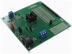
Figure 4 shows the BUF22821EVM with the test point, switch, and jumper locations noted.
Figure 4. BUF22821EVM Switch and Jumper Locations
4
BUF22821EVM Evaluation Board and Software Tutorial
SBOU053 – September 2007
Submit Documentation Feedback
�www.ti.com
EVM Operation
4.1
BKSEL
The BKSEL switch (illustrated in Figure 5) selects the memory bank to be used when operating the EVM.
Bank 1 selects the gamma curve that is stored in Bank_0 of the BUF22821. Bank 2 selects the gamma
curve that is stored in Bank_1 of the BUF22821.
The SCL and SDA jumpers must be installed on the EVM in order to allow communication between the
board and the BUF22821. The communications cable must be connected to COM1 or another COM port
on your PC.
Figure 5. BKSEL Switch
4.2
JP1
Jumper JP1 is used to set the I2C address pin of the BUF22821 to logic high or logic low. When J1 is in
the position shown in Figure 6, A0 on the BUF22821 is connected to DVDD (logic '1'). Note that the
software Change Address button must be as shown in Figure 6 for A0 = '1'.
Figure 6. BUF22821EVM Jumper JP1 Set for Logic '1'
When JP1 is in the position shown in Figure 7, A0 on the BUF22821 is connected to GND (logic '0'). Note
that the software must be as shown in Figure 7 for an address of A0 = '0'.
Figure 7. BUF22821EVM Jumper JP1 Set for Logic '0'
SBOU053 – September 2007
Submit Documentation Feedback
BUF22821EVM Evaluation Board and Software Tutorial
5
�www.ti.com
EVM Operation
4.3
JP2
Jumper JP2 selects either the BKSEL switch on the EVM or an external signal to switch between the two
nonvolatile memory banks of the BUF22821. When JP2 is in the position shown in Figure 8, the BKSEL
switch is used to switch between the memory banks
Figure 8. BUF22821EVM Jumper JP2 Set for BKSEL Switching
When JP2 is in the position shown in Figure 9, the memory banks are switched according to the external
signal applied via the connector.
Figure 9. BUF22821EVM Jumper JP2 Set for External Signal Switching
6
BUF22821EVM Evaluation Board and Software Tutorial
SBOU053 – September 2007
Submit Documentation Feedback
�www.ti.com
EVM Operation
4.4
STATOUTH
The output of STATOUTH is preset with resistors R9 and R10, as shown in Figure 10. These resistors
form a voltage divider from VS to GND. STATOUTL is preset with resistors R7 and R8.
All four resistors are installed on the EVM at the factory.
Note: Resistors R7 through R10 are installed at the factory.
Figure 10. STATOUTH Settings
SBOU053 – September 2007
Submit Documentation Feedback
BUF22821EVM Evaluation Board and Software Tutorial
7
�www.ti.com
Using the BUF22821EVM Software
5
Using the BUF22821EVM Software
Figure 11 shows the EVM software interface.
Figure 11. BUF22821EVM Software GUI
8
BUF22821EVM Evaluation Board and Software Tutorial
SBOU053 – September 2007
Submit Documentation Feedback
�www.ti.com
Using the BUF22821EVM Software
5.1
Change Address Button
Pressing the Change Address button (located near the top of the interface) changes the I2C address that
the software writes to. In Figure 11, the address is A0 = '0'. Pressing the button changes it to A0 = '1'.
Note that the Change Address button is color-coded to help you quickly identify the current address. Red
indicates that the address is A0 = '0'.
The interface also displays the last power-supply value used for the new address. This feature is helpful
when changing back to an address that was previously used.
Whenever the address is changed, a Read DAC command is automatically performed so that all the DAC
output displays are updated.
5.2
Measuring the Power Supply
You must measure the power supply (VS) value against GND, and then enter it in the Vsup field of the
software interface, as shown in Figure 12. The voltage out of each DAC is calculated according to the VS
value entered.
Figure 12. Power Supply Measurement and Recording
Measure VS at the location indicated in Figure 4.
SBOU053 – September 2007
Submit Documentation Feedback
BUF22821EVM Evaluation Board and Software Tutorial
9
�www.ti.com
Using the BUF22821EVM Software
For example, changing the value in the DAC 19 cell immediately changes the output of DAC19 to 0.996V.
The calculation is performed according to Equation 1.
VDAC_CHANNEL = VS ξ Code_in_decimal
1024
(1)
For example:
DAC 19: Code 44 (hexadecimal) = 68 (decimal)
VDAC_CHANNEL = 15V ξ 68 / 1024 = 0.996V
5.3
Reset and Read DAC Buttons
Push the ReadDAC button to read the binary value in the DAC output registers of the BUF22821. Pushing
the Reset button forces an I2C general call reset and causes all registers in the BUF22821 to reset to the
respective default values (mid-code or VS/2). Figure 13 illustrates the Reset and Read DAC buttons.
Figure 13. Reset and Read DAC Buttons
5.4
Save to File
The register configurations of the BUF22821 DACs are displayed in both analog voltage and in
hexadecimal (see Figure 12). The DAC codes (that is, gamma voltages) can be saved into a text file using
the Save to File button.
10
BUF22821EVM Evaluation Board and Software Tutorial
SBOU053 – September 2007
Submit Documentation Feedback
�www.ti.com
Using the BUF22821EVM Software
Pressing the Save to File button opens a file-save dialog box similar to that shown in Figure 14. Pressing
the folder icon creates a new folder on your PC. It is a good idea to create a directory exclusively for
BUF22821 DAC code (gamma voltage) files. Enter a unique file name in the File name field to store your
BUF22821 register information. Press the Open button to save the file.
Figure 14. Save to File Dialog Box
SBOU053 – September 2007
Submit Documentation Feedback
BUF22821EVM Evaluation Board and Software Tutorial
11
�www.ti.com
Using the BUF22821EVM Software
Saving the BUF22821 DAC codes (gamma voltages) creates a text file that can be opened in a
spreadsheet program or text editor, as illustrated in Figure 15.
Figure 15. Working with a Saved BUF22821 Data File
The first entry in the file is the power-supply value. Fields 2 through 19 contain the DAC codes (decimal)
for Outputs 1 through 18. Fields 20 and 21 contain the DAC codes (decimal) for VCOM1 and VCOM2. Fields
22 through 25 contain the DAC codes (decimal) for Outputs 19 through 22.
12
BUF22821EVM Evaluation Board and Software Tutorial
SBOU053 – September 2007
Submit Documentation Feedback
�www.ti.com
Using the BUF22821EVM Software
5.5
Loading a Saved Data File
The BUF22821EVM software is also able to load data saved from previous evaluations. A saved register
configuration can be loaded into the BUF22821 using the Load From File button, shown in Figure 16. The
program remembers where you saved the last register configuration. Simply select the desired
configuration and press Open.
Figure 16. Load From File Button
SBOU053 – September 2007
Submit Documentation Feedback
BUF22821EVM Evaluation Board and Software Tutorial
13
�www.ti.com
Using the BUF22821EVM Software
5.6
Changing the DAC Analog Voltage
The analog voltage of any DAC can be directly edited, as Figure 17 shows.
Figure 17. Changing the DAC Analog Voltage
14
BUF22821EVM Evaluation Board and Software Tutorial
SBOU053 – September 2007
Submit Documentation Feedback
�www.ti.com
Using the BUF22821EVM Software
Note, however, that the hexadecimal value associated with the DAC updates according to changes in the
analog voltage, but it cannot be directly edited.
If you select a DAC and click on the up arrow control, the DAC register increases by one count.
Conversely, clicking on the down arrow control decreases the DAC register by one count.
5.7
Run Batch Button
The Run Batch button (as noted in Figure 18) enables the user to configure the BUF22821 to cycle
through different register configurations in a continuous loop. When connected to the end application, this
feature can be used to cycle through different gamma settings to determine what the optimal settings must
be for a given application.
When the Run Batch button is pressed, a new dialog box displays, as shown in Figure 18. The delay time
is the amount of time in between loading new configurations into the BUF22821.
Figure 18. Run Batch Dialog Box
Use the Single Step Up and Single Step Down buttons to step through the selected files manually. The
currently-selected file name is displayed in the lower left corner area of the dialog box. Press the
key and click on the files you want to select. In Figure 18, two configuration files are selected.
SBOU053 – September 2007
Submit Documentation Feedback
BUF22821EVM Evaluation Board and Software Tutorial
15
�www.ti.com
Using the BUF22821EVM Software
5.8
Control Panel
Pressing the Control Panel button brings up a display panel that allows you to adjust each channel using a
set of graphical sliders, as shown in Figure 19. Simply drag the slider to adjust the desired channel output.
The DAC output value changes automatically.
Figure 19. Control Panel Button and Graphical Sliders
16
BUF22821EVM Evaluation Board and Software Tutorial
SBOU053 – September 2007
Submit Documentation Feedback
�www.ti.com
Using the BUF22821EVM Software
5.9
Program OTP All Channels Button
As Figure 20 shows, pressing the Program OTP All Channels button allows you to program a gamma
curve into the nonvolatile memory in the BUF22821. All 22 channels (including the VCOM channels) are
then programmed simultaneously. The values are stored in the memory bank that is selected via the
BKSEL switch (see Section 4.1). Note that Bank 1 corresponds to Bank_0 inside the BUF22821, while
Bank 2 corresponds to Bank_1.
Figure 20. Program OTP All Channels Button
5.10 Program OTP Out Button
Pressing the Program OTP Out button (illustrated in Figure 21) allows you to store the value of a specific
channel into the nonvolatile memory in the BUF22821. This feature is useful when the VCOM channels
must be programmed at different times. The values are stored in the memory bank that is selected via the
BKSEL switch. The Write OTP Reg dialog box appears.
Figure 21. Program OTP Out Button and Write OTP Reg Dialog
In the example shown in Figure 21, to program 0.996V into the nonvolatile memory of channel 19, use the
up and down arrows to select channel 19. Then press the Write Selected Reg to OTP button.
SBOU053 – September 2007
Submit Documentation Feedback
BUF22821EVM Evaluation Board and Software Tutorial
17
�www.ti.com
Hardware and Schematic
5.11 Max Bank Field
The Max Bank field at the top of the software interface (see Figure 22) shows how many times the
memory of the most-programmed channel of the selected memory bank has been previously written.
• None: Max bank shows 0.
• Once: Max Bank shows 0.
• Twice: Max bank shows 1.
• Three times: Max bank shows 2.
• 16 times: Max bank shows 15.
Figure 22. Max Bank Field
6
Hardware and Schematic
This section contains the complete bill of materials, schematic diagram, and PCB layouts for the
BUF22821EVM.
Note: Board layouts are not to scale. These are intended to show how the board is laid out; they
are not intended to be used for manufacturing BUF22821EVM PCBs.
18
BUF22821EVM Evaluation Board and Software Tutorial
SBOU053 – September 2007
Submit Documentation Feedback
�SBOU053 – September 2007
Submit Documentation Feedback
J4
Vsd
Vs
8
7
6
5
4
3
2
1
.1uF
C12
J2
1
2
+
0.1uF
C14
S1
1
F5
F4
F3
F2
F1
R19
10k
1
Vin
U6
C11
U7
Adj
Vout
10k
250k
R6
C4 +
Vsd
10k
R1
1.5uF
0.1uF
C19
2
C3
U5
5.76k
R21
10uF
R20
4
5
+
Vsd
10uF
C10 +
R5 (Optional- Not populated)
Vin
TPS79901-DDC
Com
Vout
3
/Tab Vsd
UA78M33 REGULATOR
10uF
C9
4 uH
L1
1.5uF
Vsd
4
0.1uF
C13
Vsd 2.0V
Vs
1
2
3
4
5
6
7
8
9
10
11
12
13
14
U2
Texas
Instruments
MAX3238
10uF
C2 + C1
JP2
0.1uF
C18
Vsd 2.0V
28
27
26
25
24
23
22
21
20
19
18
17
16
15
0.1uF
Vs
C5
.22uF
C16
0.1uF
1.5uF
C6 +
1k
1
2
3
4
5
6
7
8
9
10
11
12
13
14
15
16
17
18
19
STATINH
TP STATINH
R10
1
2
3
1
2
3
U4
U3
4
5
4
5
38
37
36
35
34
33
32
31
30
29
28
27
26
25
24
23
22
21
20
Vs
TP STATINL
C8
0.1uF
R3
R2
Vsd Vsd 2.0V
STATINL
1k 75k
C7
0.1uF
BUF22821
U1
75k
R9 R8 R7
Vs
4.7k
4.7k
JP6
JP5
SCL
TP SCL
SDA TP SDA
Vsd 2.0V
1
2
L
3 H JP1
A0
R11 1k
RA-RZ are all 0.0 Ohms
RZ
RY
RX
RW
RV
RU
RT
RS
RR
RQ
RP
RO
RN
RM
RL
RK
RJ
RI
RH
RG
RF
RE
RD
RC
RB
RA
1
2
3
J1
SDA
SCL
BKSEL
Parts Optional- Not Populated
Vs
TP Gnd
26
25
24
23
22
21
20
19
18
17
16
15
14
13
12
11
10
9
8
7
6
5
4
3
2
1
JP3
TP Vs
6.1
Vsd 2.0V
Vs
Gnd
L2
www.ti.com
Hardware and Schematic
Schematic
Figure 23 shows the schematic for the BUF22821EVM.
+
Figure 23. BUF22821EVM Schematic
BUF22821EVM Evaluation Board and Software Tutorial
19
�www.ti.com
Hardware and Schematic
6.2
PCB Layouts
Figure 24 and Figure 25 show the PCB layout of the BUF22821EVM.
Figure 24. BUF22821EVM PCB Top Layer (Component Side)
20
BUF22821EVM Evaluation Board and Software Tutorial
SBOU053 – September 2007
Submit Documentation Feedback
�www.ti.com
Hardware and Schematic
Figure 25. BUF22821EVM PCB Bottom Layer (Solder Side)
SBOU053 – September 2007
Submit Documentation Feedback
BUF22821EVM Evaluation Board and Software Tutorial
21
�www.ti.com
Hardware and Schematic
6.3
Bill of Materials
Table 1 lists the bill of materials for this EVM.
Table 1. Bill of Materials
Count
9
22
RefDes
Description
C1, C7–C8,
C12–C14, C16,
C18–C19
Capacitor, Ceramic, 0.1μF, 603 size
2
C2, C11
3
C3, C4, C6
1
Part Number
MFR
C1608X7R1E104K
TDK
Capacitor, Tantalum, 10μF, 10V, SMT 3216 "A"
T491A106K010AT
Kemet
Capacitor, Tantalum, 1.5μF, 16V, SMT 3216 "A"
T491A155K016AT
Kemet
C5
Capacitor, Ceramic, 0.22μF, 1206
C1608X7R1C224K
TDK
2
C9, C10
Capacitor, Tantalum, 10μF, 20V, SMT 3528 "B"
B45196H4106M209
Kemet
5
F1–F6
Ferrite Bead, 600Ω at 100MHz, SM 0603
HZ0603C601R-10
Steward
1
J1
Terminal Strip, 3-Position, Cage Clamp, 45°,
Dove-tailed
ED300/3
On-Shore
Technology Inc
1
J2
Terminal Strip, 2-Position, Cage Clamp, 45°,
Dove-tailed
ED300/2
On-Shore
Technology Inc
1
J4
Connector, Modular Receptacle, RJ-45, Side Entry,
8 position/ 8 contact
5520426-4
AMP Tyco
Electronics
1
L1
Inductor, 150μH, 1210 SMD 10%
ELJ-FA151KF
Panasonic
1
L2
Inductor, 3.9μH, 1210 SMD 10%
ELJ-FA3R9KF
Panasonic
1
R1
Resistor, 10kΩ, 603 size
CRCW060310K0FKEA
Vishay/Dale
2
R19, R20
Resistor, 10kΩ, 1206 size
CRCW120610K0FKEA
Vishay/Dale
2
R2, R3
Resistor, 4.7kΩ, 603 size
CRCW06034K70FKEA
Vishay/Dale
1
R21
Resistor, 6.81kΩ, 1206 size
CRCW12066K81FKEA
Vishay/Dale
0
R5
Resistor, 603 size.
OPTIONAL; NOT NORMALLY INSTALLED.
1
R6
Resistor, 249kΩ, 603 size
CRCW0603249KFKEA
Vishay/Dale
2
R7, R9
Resistor, 75kΩ, 1206 size
CRCW120675K0FKEA
Vishay/Dale
3
R8, R10, R11
Resistor, 1kΩ, 1206 size
CRCW12061K00FKEA
Vishay/Dale
Vishay/Dale
26
RA–RZ
Resistor, 0.0Ω, 603 size
CRCW06030000Z0EA
1
S1
Switch, Toggle, SPDT, .4VA, PC Mount
200AWMSP1T1A1M2RE
E-Switch
1
JP3
Terminal Strip, 26 position, .100 centers, .025 square
pins
TSW-126-07-G-S
Samtec
2
JP1, JP2
Terminal Strip, 3 position, .100 centers, .025 square
pins
TSW-103-07-G-S
Samtec
2
JP5, JP6
Terminal Strip, 2 position, .100 centers, .025 square
pins
TSW-102-07-G-S
Samtec
9
XXXXX TP (All)
Terminal Strip, 1 position, .100 centers, .025 square
pins
TSW-101-07-G-S
Samtec
1
U1
Socket, TSSOP 38-Pin ZIF
OTS-38(44)-0.5-01
ENPLAS
1
U2
IC, 3V to 5.5V MultiChannel RS-232 Line
Driver/Receiver, TSSOP-28
MAX3238CPWR
Texas Instruments
2
U3, U4
IC, Single Buffer/Driver w/Open Drain Out, SOT23-5
SN74LVC1G07DB
Texas Instruments
1
U5
IC, Single Buffer, Schmitt Trigger, SOT23-5
SN74LVC1G17DB
Texas Instruments
1
U6
IC, Voltage Regulator, 3.3V, SOT223-4
UA78M33CDCYR
Texas Instruments
1
U7
IC, Voltage Regulator, Adjustable, TSOT23-5
TPS79901DDC
Texas Instruments
4
Standoff, Hex 4-40 Aluminum. 0.500in
2203
Keystone
Electronics
4
Screw, Machine, Phillips, 4-40X1/4 SS
PMSSS 440 0025 PH
Building Fasteners
4
Shunt, w/ handle, 2 pos, 0.100in
881545-2
AMP Tyco
Electronics
BUF22821EVM Evaluation Board and Software Tutorial
SBOU053 – September 2007
Submit Documentation Feedback
�EVALUATION BOARD/KIT IMPORTANT NOTICE
Texas Instruments (TI) provides the enclosed product(s) under the following conditions:
This evaluation board/kit is intended for use for ENGINEERING DEVELOPMENT, DEMONSTRATION, OR EVALUATION PURPOSES
ONLY and is not considered by TI to be a finished end-product fit for general consumer use. Persons handling the product(s) must have
electronics training and observe good engineering practice standards. As such, the goods being provided are not intended to be complete
in terms of required design-, marketing-, and/or manufacturing-related protective considerations, including product safety and environmental
measures typically found in end products that incorporate such semiconductor components or circuit boards. This evaluation board/kit does
not fall within the scope of the European Union directives regarding electromagnetic compatibility, restricted substances (RoHS), recycling
(WEEE), FCC, CE or UL, and therefore may not meet the technical requirements of these directives or other related directives.
Should this evaluation board/kit not meet the specifications indicated in the User’s Guide, the board/kit may be returned within 30 days from
the date of delivery for a full refund. THE FOREGOING WARRANTY IS THE EXCLUSIVE WARRANTY MADE BY SELLER TO BUYER
AND IS IN LIEU OF ALL OTHER WARRANTIES, EXPRESSED, IMPLIED, OR STATUTORY, INCLUDING ANY WARRANTY OF
MERCHANTABILITY OR FITNESS FOR ANY PARTICULAR PURPOSE.
The user assumes all responsibility and liability for proper and safe handling of the goods. Further, the user indemnifies TI from all claims
arising from the handling or use of the goods. Due to the open construction of the product, it is the user’s responsibility to take any and all
appropriate precautions with regard to electrostatic discharge.
EXCEPT TO THE EXTENT OF THE INDEMNITY SET FORTH ABOVE, NEITHER PARTY SHALL BE LIABLE TO THE OTHER FOR ANY
INDIRECT, SPECIAL, INCIDENTAL, OR CONSEQUENTIAL DAMAGES.
TI currently deals with a variety of customers for products, and therefore our arrangement with the user is not exclusive.
TI assumes no liability for applications assistance, customer product design, software performance, or infringement of patents or
services described herein.
Please read the User’s Guide and, specifically, the Warnings and Restrictions notice in the User’s Guide prior to handling the product. This
notice contains important safety information about temperatures and voltages. For additional information on TI’s environmental and/or
safety programs, please contact the TI application engineer or visit www.ti.com/esh.
No license is granted under any patent right or other intellectual property right of TI covering or relating to any machine, process, or
combination in which such TI products or services might be or are used.
FCC Warning
This evaluation board/kit is intended for use for ENGINEERING DEVELOPMENT, DEMONSTRATION, OR EVALUATION PURPOSES
ONLY and is not considered by TI to be a finished end-product fit for general consumer use. It generates, uses, and can radiate radio
frequency energy and has not been tested for compliance with the limits of computing devices pursuant to part 15 of FCC rules, which are
designed to provide reasonable protection against radio frequency interference. Operation of this equipment in other environments may
cause interference with radio communications, in which case the user at his own expense will be required to take whatever measures may
be required to correct this interference.
EVM WARNINGS AND RESTRICTIONS
It is important to operate this EVM within the input voltage range of 9V (min) to 20V (max) and the output voltage range of 9V (min) to 20V
(max).
Exceeding the specified input range may cause unexpected operation and/or irreversible damage to the EVM. If there are questions
concerning the input range, please contact a TI field representative prior to connecting the input power.
Applying loads outside of the specified output range may result in unintended operation and/or possible permanent damage to the EVM.
Please consult the EVM User's Guide prior to connecting any load to the EVM output. If there is uncertainty as to the load specification,
please contact a TI field representative.
During normal operation, some circuit components may have case temperatures greater than +25°C. The EVM is designed to operate
properly with certain components above +25°C as long as the input and output ranges are maintained. These components include but are
not limited to linear regulators, switching transistors, pass transistors, and current sense resistors. These types of devices can be identified
using the EVM schematic located in the EVM User's Guide. When placing measurement probes near these devices during operation,
please be aware that these devices may be very warm to the touch.
Mailing Address: Texas Instruments, Post Office Box 655303, Dallas, Texas 75265
Copyright © 2007, Texas Instruments Incorporated
�IMPORTANT NOTICE AND DISCLAIMER
TI PROVIDES TECHNICAL AND RELIABILITY DATA (INCLUDING DATASHEETS), DESIGN RESOURCES (INCLUDING REFERENCE
DESIGNS), APPLICATION OR OTHER DESIGN ADVICE, WEB TOOLS, SAFETY INFORMATION, AND OTHER RESOURCES “AS IS”
AND WITH ALL FAULTS, AND DISCLAIMS ALL WARRANTIES, EXPRESS AND IMPLIED, INCLUDING WITHOUT LIMITATION ANY
IMPLIED WARRANTIES OF MERCHANTABILITY, FITNESS FOR A PARTICULAR PURPOSE OR NON-INFRINGEMENT OF THIRD
PARTY INTELLECTUAL PROPERTY RIGHTS.
These resources are intended for skilled developers designing with TI products. You are solely responsible for (1) selecting the appropriate
TI products for your application, (2) designing, validating and testing your application, and (3) ensuring your application meets applicable
standards, and any other safety, security, or other requirements. These resources are subject to change without notice. TI grants you
permission to use these resources only for development of an application that uses the TI products described in the resource. Other
reproduction and display of these resources is prohibited. No license is granted to any other TI intellectual property right or to any third
party intellectual property right. TI disclaims responsibility for, and you will fully indemnify TI and its representatives against, any claims,
damages, costs, losses, and liabilities arising out of your use of these resources.
TI’s products are provided subject to TI’s Terms of Sale (www.ti.com/legal/termsofsale.html) or other applicable terms available either on
ti.com or provided in conjunction with such TI products. TI’s provision of these resources does not expand or otherwise alter TI’s applicable
warranties or warranty disclaimers for TI products.
Mailing Address: Texas Instruments, Post Office Box 655303, Dallas, Texas 75265
Copyright © 2019, Texas Instruments Incorporated
�