User’s Guide
SNLU103—May2012
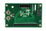
C185EKV01 User’s Guide
CONTENTS
1.
INTRODUCTION........................................................................................................ 2
2.
SETUP ....................................................................................................................... 3
3.
BOARD LAYOUT ...................................................................................................... 6
4.
SCHEMATIC ............................................................................................................ 10
LIST OF FIGURES
Figure 1: Default Jumper Settings ................................................................................................................................3
Figure 2: LVDS Output Connections ............................................................................................................................4
Figure 3: LVCMOS Input Connections .........................................................................................................................5
Figure 4: Top Assembly Layer ......................................................................................................................................7
Figure 5: Top Layer Routing .........................................................................................................................................8
Figure 6: Bottom Layer Routing ....................................................................................................................................9
Figure 7: C185EV01 Schematic Page 1 .....................................................................................................................10
Figure 8: C185EV01 Schematic Page 1 .....................................................................................................................11
LIST OF TABLES
Table 1: Device and Package Configurations...............................................................................................................2
Table 2: C185EV01 Bill of Materials ...........................................................................................................................12
TRI-STATE is a registered trademark of Texas Instruments
SNLU103-May 2012
Submit Documentation Feedback
C185EVK01 User’s Guide
1
�Introduction
1.
Introduction
The Texas Instruments C185EVK01 evaluation module (EVK) helps designers evaluate the operation and
performance of the DS90C185 Low Power 1.8V FPD-Link (LVDS) Serializer. The device operates off of a
single 1.8V supply and supports input pixel clocks from 25 MHz to 105 MHz.
1.8V
LVCMOS
GPU
R7-R0
G7-G0
B7-B0
1.8V
DS90C185
FPD-Link
SERIALIZER
LVDS0+/LVDS1+/LVDS2+/LVDSC+/LVDS3+/-
HSync
VSync
DE
GPO/CNTL(L/R)
CLK
FPD-Link
4D+C
LVDS
DISPLAY MODULE
SXGA+ Resolution
TCON
w/ LVDS Interface
PDB
The EVM contains one Low Power 1.8V FPD-Link (LVDS) Serializer (See Table 1).
Table 1: Device and Package Configurations
SERIALIZER
U1
2
C185EVK01 User’s Guide
IC
DS90C185SQ
PACKAGE
SQF48A
SNLU103-May 2012
Submit Documentation Feedback
�Setup
2.
Setup
This section describes the jumpers and connectors on the EVK as well and how to properly connect, set up
and use the C185EVK01.
2.1. Input/Output Connector Description
JP1 – PDB is the jumper used to enable the Serializer. Power Down Bar (PDB) set to logic HIGH enables the
device, while connecting this jumper to logic LOW will disable the device.
JP2 – VODSEL is the jumper that controls the differential output voltage. When VODSEL is set to logic
HIGH, the output launch amplitude of the LVDS drivers will be set to have a larger output swing. If this jumper
is set to logic LOW, then the LVDS drivers will be configured to have a power saving smaller output swing.
JP3 – RFB is the jumper that selects the clock edge that the input LVCMOS data will be sampled on. If RFB
is logic HIGH, the input data is latched on the RISING EDGE of the pixel clock. If RFB is set to logic LOW,
the input data is latched on the FALLING EDGE of the pixel clock.
Figure 1: Falling Edge Data Strobe
Figure 2: Rising Edge Data Strobe
JP4 – 18B_MODE is the jumper used to enable a power saving mode for 18-bit color applications. When this
jumper is set to logic LOW, all data inputs will be sampled, serialized and driven out through the LVDS drivers
to support 24-bit color applications or 28-bit generic data buses. If this jumper is set to logic HIGH, the device
will enter a power saving mode that will power down the circuitry that feeds the 4th LVDS driver. In this mode
the 4th LVDS driver, TxOUT3+/- will be TRI-STATE®.
Figure 3: Default Jumper Settings
SNLU103-May 2012
Submit Documentation Feedback
H
C185EVK01 User’s Guide
3
�Setup
J1 – LVDS OUTPUTS are brought out to a 2 x10 bank of header pins. Note that each LVDS output is
separated from adjacent LVDS signals by one ground pin. By default, 100 ohm termination resistors are
soldered onto the EVM to allow for easy measuring and probing of the LVDS signals. If a cable is
connected to J1, these termination resistors (R57, R58, R62, R63, R64) must be removed or the
differential voltage swing will be reduced.
Figure 4: LVDS Output Connections (J1)
J2 – LVCMOS INPUTS are connected to the 2 x 30 bank of header pins. Note that each LVCMOS signal is
paired with a ground signal. When attaching external test equipment or other hardware to this board it is
important that there be sufficient ground connections to ensure good signal integrity for the input clock and
data waveforms. There is a provision to populate 50 ohm terminations if needed.
4
C185EVK01 User’s Guide
SNLU103-May 2012
Submit Documentation Feedback
�Setup
Figure 5: LVCMOS Input Connections (J2)
J3 – VDD is the terminal where 1.8V power should be applied.
J4 – GND is the terminal where ground should be applied.
2.2. System Setup
The input power jack (J3) should receive a voltage within the range of 1.71 V to 1.89 V. Once, power has
been applied to the board, the PDB pin can be set to logic HIGH. After setting the PDB pin to HIGH, 1.8V
clock and data can be transmitted to the EVM. If a cable is connected to J1, the termination resistors
(R57, R58, R62, R63, R64) should be removed.
SNLU103-May 2012
Submit Documentation Feedback
C185EVK01 User’s Guide
5
�Setup
2.3. Operation
For proper operation of the DS90C185, JP1, JP2, JP3 and JP4 should be properly configured by using
shorting blocks (jumpers); see Figure 3.
JP1 to HIGH, after power on
JP2 to LOW for reduced VOD swing or HIGH for large VOD swing
JP3 to LOW for falling clock edge strobe or HIGH for rising clock edge strobe
JP4 to LOW for 24-bit color (28-bit data bus) or to HIGH for 18-bit color (21-bit data bus)
After applying power and setting JP1 to HIGH, a clock signal can be sent to the DS90C185. When the clock
signal is detected, the DS90C185 will power on and begin to transmit serialized LVDS data.
.
3.
Board Layout
Figure 4, Figure 5 and Figure 6 show the board layout for the C185EV01 printed circuit board. The EVM
offers jumpers to configure and power on/off the DS90C185. Resistor pads are provided so that 50 ohm
shunt terminations can be implemented when interfacing with external video (data) generators with 50 ohm
signal sources. 100 ohm differential termination resistors are populated by default to allow for probing of the
LVDS outputs at J1.
6
C185EVK01 User’s Guide
SNLU103-May 2012
Submit Documentation Feedback
�Board Layout
Figure 6: Top Assembly Layer
SNLU103-May 2012
Submit Documentation Feedback
C185EVK01 User’s Guide
7
�Board Layout
Figure 7: Top Layer Routing
8
C185EVK01 User’s Guide
SNLU103-May 2012
Submit Documentation Feedback
�Board Layout
Figure 8: Bottom Layer Routing
SNLU103-May 2012
Submit Documentation Feedback
C185EVK01 User’s Guide
9
�2
GND
2 1
49
R57
100
0201
DAP
R58
100
0201
J1
TxOUT0+
2 1
GND0
24
15
13
VDDPLL
TxOUT2TxOUT2+
TxCLKOUTTxCLKOUT+
VODSEL
TxOUT1TxOUT1+
32
31
TxOUT2TxOUT2+
30
29
TxCLKOUTTxCLKOUT+
28
27
TxOUT3TxOUT3+
TxOUT2+
TxCLKOUT+
2 1
34
33
R63
100
0201
TxOUT3+
JP1
TxOUT2TxCLKOUTTxOUT3-
GND
VDD
1
2
3
VDD
RFB
GND
1
2
3
VDD
18B_MODE
GND
1
2
3
VDD
JP4
PDB
GND
VODSEL
GND
VODSEL
18B_MODE
PDB
TxOUT1-
JP3
1
2
3
JP2
RFB
TxOUT0-
R64
100
0201
39
26
18B_MODE
TxOUT3TxOUT3+
TxOUT0TxOUT0+
R62
100
0201
2
4
6
8
10
12
14
16
18
20
2 1
TxOUT1TxOUT1+
36
35
TxOUT1+
1
3
5
7
9
11
13
15
17
19
1
TxOUT0TxOUT0+
23
DS90C185
GND1
VDD
48
CLK
D0
D1
D2
D3
D4
D5
D6
D7
D8
D9
D10
D11
D12
D13
D14
D15
D16
D17
D18
D19
D20
D21
D22
D23
D24
D25
D26
D27
PDB
6
38
40
41
42
43
44
45
46
47
1
2
3
4
5
7
8
9
10
11
12
14
16
17
18
19
20
21
22
RFB
CLK
D0
D1
D2
D3
D4
D5
D6
D7
D8
D9
D10
D11
D12
D13
D14
D15
D16
D17
D18
D19
D20
D21
D22
D23
D24
D25
D26
D27
37
CLK
D0
D1
D2
D3
D4
D5
D6
D7
D8
D9
D10
D11
D12
D13
D14
D15
D16
D17
D18
D19
D20
D21
D22
D23
D24
D25
D26
D27
VDD
U1
25
VDDTX
Schematic
VDDTX
4.
VDDPLL
Schematic
Figure 9: C185EVK01 Schematic Page 1
10
C185EVK01 User’s Guide
SNLU103-May 2012
Submit Documentation Feedback
�Schematic
C11
1 201 R312
49.9ohm_open
1 201 R302
49.9ohm_open
1 201 R292
49.9ohm_open
1 201 R282
49.9ohm_open
1 201 R272
49.9ohm_open
1 201 R262
49.9ohm_open
1 201 R252
49.9ohm_open
1
C12
CLK
D0
D1
D2
D3
D4
D5
D6
D7
D8
D9
D10
D11
D12
D13
D14
D15
D16
D17
D18
D19
D20
D21
D22
D23
D24
D25
D26
D27
GND
VDDTX
1
1 201 R242
49.9ohm_open
1 201 R232
49.9ohm_open
1 201 R222
49.9ohm_open
1 201 R212
49.9ohm_open
1 201 R202
49.9ohm_open
2
R1
1
0 Ohm,0402
1
VDD_b
1 201 R192
49.9ohm_open
1 201 R182
49.9ohm_open
1 201 R172
49.9ohm_open
1 201 R162
49.9ohm_open
1 201 R152
49.9ohm_open
1 201 R142
49.9ohm_open
1 201 R132
49.9ohm_open
1 201 R122
49.9ohm_open
1 201 R112
49.9ohm_open
1 201 R102
49.9ohm_open
1 201
R92
49.9ohm_open
1 201
R82
49.9ohm_open
1 201
R72
49.9ohm_open
GND
1 201 R322
49.9ohm_open
CLK
D0
D1
D2
D3
D4
D5
D6
D7
D8
D9
D10
D11
D12
D13
D14
D15
D16
D17
D18
D19
D20
D21
D22
D23
D24
D25
D26
D27
2
4
6
8
10
12
14
16
18
20
22
24
26
28
30
32
34
36
38
40
42
44
46
48
50
52
54
56
58
60
1 201
R62
49.9ohm_open
2
4
6
8
10
12
14
16
18
20
22
24
26
28
30
32
34
36
38
40
42
44
46
48
50
52
54
56
58
60
1 201
R52
49.9ohm_open
1
3
5
7
9
11
13
15
17
19
21
23
25
27
29
31
33
35
37
39
41
43
45
47
49
51
53
55
57
59
1 201
R42
49.9ohm_open
1
3
5
7
9
11
13
15
17
19
21
23
25
27
29
31
33
35
37
39
41
43
45
47
49
51
53
55
57
59
HEADER 30x2
J2
+
C10
22uF
2
2
2
0.01uF 0.1uF
GND
C2
+
C3
VDD_b
+
2
R2
1
0 Ohm,0402
C15
+
C13
22uF
0.01uF 0.1uF
GND
2
GND
C14
0.1uF
2
1
2.2uF
2
1
2
22uF
2
J4
VDD
1
+
1
C1
2
BANANA
1
VDD_b
1
1
1
1
1
J3
C18
1
2
R3
1
0 Ohm,0402
1
VDD_b
VDDPLL
1
BANANA
C17
+
C16
22uF
2
2
2
0.01uF 0.1uF
GND
Figure 10: C185EVK01 Schematic Page 1
SNLU103-May 2012
Submit Documentation Feedback
C185EVK01 User’s Guide
11
�Schematic
Table 2: C185EVK01 Bill of Materials
Quantity
1
1
1
3
3
3
4
1
1
2
3
29
5
1
12
Reference Designator
C1
C2
C3
C10,C13,C16
C11,C14,C17
C12,C15,C18
JP1,JP2,JP3,JP4
J1
J2
J3,J4
R1,R2,R3
Part
22uF
2.2uF
0.1uF
22uF
0.1uF
0.01uF
3-Pin Header
2X10 Pin Header
30x2 Pin Header
BANANA
0 Ohm, 0402
Vendor
Nichicon
KEMET
KEMET
Kemet
Panasonic
KEMET
AMP/Tyco
3M
AMP/Tyco
Johnson
Panasonic
Part number
F931E226MNC
T491B225K020AT
C1206C104K5RACTU
T494B226M016AT
ECJ-1VB1E104K
C0603C103K1RACTU
87224-3
N2520-6002RB
3-87215-0
108-0740-001
ERJ-2GEJ0R00X
R4,R5,R6,R7,R8,R9,R10,R11,R12
,R13,R14,R15,R16,R17,R18,R19,
R20,R21,R22,R23,R24,R25,R26,
R27,R28,R29,R30,R31,R32
R57,R58,R62,R63,R64
U1
49.9ohm_open
100 ohm
DS90C185
Panasonic
Susumu
TI
ERJ-1GEF49R9C_open
RR0306P-101-D
DS90C185SQ
C185EVK01 User’s Guide
SNLU103-May 2012
Submit Documentation Feedback
�FCC Warning
This evaluation board/kit is intended for use for ENGINEERING DEVELOPMENT, DEMONSTRATION, OR EVALUATION
PURPOSES ONLY and is not considered by TI to be a finished end-product fit for general customer use. It generates, uses, and can radiate
radio frequency energy and has not been tested for compliance with the limits of computing devices pursuant to part 15 of FCC rules, which are
designed to provide reasonable protection against radio frequency interference. Operation of this equipment in other environments may cause
interference with radio communications, in which case the user at his own expense will be required to take whatever measures may be required
to correct this interference.
EVALUATION BOARD/KIT IMPORTANT NOTICE
Texas Instruments (TI) provides the enclosed product(s) under the following conditions:
This evaluation board/kit is intended for use for ENGINEERING DEVELOPMENT, DEMONSTRATION, OR EVALUATION PURPOSES ONLY
and is not considered by TI to be a finished end-product fit for general consumer use. Persons handling the product(s) must have electronics
training and observe good engineering practice standards. As such, the goods being provided are not intended to be complete in terms of
required design-, marketing-, and/or manufacturing-related protective considerations, including product safety and environmental measures
typically found in end products that incorporate such semiconductor components or circuit boards. This evaluation board/kit does not fall within
the scope of the European Union directives regarding electromagnetic compatibility, restricted substances (RoHS), recycling (WEEE), FCC, CE
or UL, and therefore may not meet the technical requirements of these directives or other related directives.
Should this evaluation board/kit not meet the specifications indicated in the User’s Guide, the board/kit may be returned within 30 days from the
date of delivery for a full refund. THE FOREGOING WARRANTY IS THE EXCLUSIVE WARRANTY MADE BY SELLER TO BUYER AND IS IN
LIEU OF ALL OTHER WARRANTIES, EXPRESSED, IMPLIED, OR STATUTORY, INCLUDING ANY WARRANTY OF MERCHANTABILITY OR
FITNESS FOR ANY PARTICULAR PURPOSE.
The user assumes all responsibility and liability for proper and safe handling of the goods. Further, the user indemnifies TI from all claims arising
from the handling or use of the goods. Due to the open construction of the product, it is the user’s responsibility to take any and all appropriate
precautions with regard to electrostatic discharge.
EXCEPT TO THE EXTENT OF THE INDEMNITY SET FORTH ABOVE, NEITHER PARTY SHALL BE LIABLE TO THE OTHER FOR ANY
INDIRECT, SPECIAL, INCIDENTAL, OR CONSEQUENTIAL DAMAGES.
TI currently deals with a variety of customers for products, and therefore our arrangement with the user is not exclusive.
TI assumes no liability for applications assistance, customer product design, software performance, or infringement of patents or
services described herein.
Please read the User’s Guide and, specifically, the Warnings and Restrictions notice in the User’s Guide prior to handling the product. This
notice contains important safety information about temperatures and voltages. For additional information on TI’s environmental and/or safety
programs, please contact the TI application engineer or visit www.ti.com/esh.
No license is granted under any patent right or other intellectual property right of TI covering or relating to any machine, process, or combination
in which such TI products or services might be or are used.
EVM WARNINGS AND RESTRICTIONS
It is important to operate this EVM within the input voltage range of -0.3 V to 48 V and the output voltage range of 0.9 V to 18 V.
Exceeding the specified input range may cause unexpected operation and/or irreversible damage to the EVM. If there are questions concerning
the input range, please contact a TI field representative prior to connecting the input power.
Applying loads outside of the specified output range may result in unintended operation and/or possible permanent damage to the EVM. Please
consult the EVM User's Guide prior to connecting any load to the EVM output. If there is uncertainty as to the load specification, please contact a
TI field representative.
During normal operation, some circuit components may have case temperatures greater than 85° C. The EVM is designed to operate properly
with certain components above 60° C as long as the input and output ranges are maintained. These components include but are not limited to
linear regulators, switching transistors, pass transistors, and current sense resistors. These types of devices can be identified using the EVM
schematic located in the EVM User's Guide. When placing measurement probes near these devices during operation, please be aware that
these devices may be very warm to the touch.
Mailing Address: Texas Instruments, Post Office Box 655303, Dallas, Texas 75265
Copyright © 2012, Texas Instruments Incorporated
�NOTES
�IMPORTANT NOTICE
Texas Instruments Incorporated and its subsidiaries (TI) reserve the right to make corrections, modifications,
enhancements, improvements, and other changes to its products and services at any time and to discontinue any
product or service without notice. Customers should obtain the latest relevant information before placing orders and
should verify that such information is current and complete. All products are sold subject to TI’s terms and conditions
of sale supplied at the time of order acknowledgment.
TI warrants performance of its hardware products to the specifications applicable at the time of sale in accordance
with TI’s standard warranty. Testing and other quality control techniques are used to the extent TI deems necessary
to support this warranty. Except where mandated by government requirements, testing of all parameters of each
product is not necessarily performed.
TI assumes no liability for applications assistance or customer product design. Customers are responsible for their
products and applications using TI components. To minimize the risks associated with customer products and
applications, customers should provide adequate design and operating safeguards.
TI does not warrant or represent that any license, either express or implied, is granted under any TI patent right,
copyright, mask work right, or other TI intellectual property right relating to any combination, machine, or process in
which TI products or services are used. Information published by TI regarding third-party products or services does
not constitute a license from TI to use such products or services or a warranty or endorsement thereof. Use of such
information may require a license from a third party under the patents or other intellectual property of the third party,
or a license from TI under the patents or other intellectual property of TI. Reproduction of information in TI data
books or data sheets is permissible only if reproduction is without alteration and is accompanied by all associated
warranties, conditions, limitations, and notices.
Reproduction of this information with alteration is an unfair and deceptive business practice. TI is not responsible or
liable for such altered documentation. Resale of TI products or services with statements different from or beyond the
parameters stated by TI for that product or service voids all express and any implied warranties for the associated TI
product or service and is an unfair and deceptive business practice. TI is not responsible or liable for any such
statements.
TI products are not authorized for use in safety-critical applications (such as life support) where a failure of the TI
product would reasonably be expected to cause severe personal injury or death, unless officers of the parties have
executed an agreement specifically governing such use. Buyers represent that they have all necessary expertise in
the safety and regulatory ramifications of their applications, and acknowledge and agree that they are solely
responsible for all legal, regulatory and safety-related requirements concerning their products and any use of TI
products in such safety-critical applications, notwithstanding any applications-related information or support that may
be provided by TI. Further, Buyers must fully indemnify TI and its representatives against any damages arising out of
the use of TI products in such safety-critical applications.
TI products are neither designed nor intended for use in military/aerospace applications or environments unless the
TI products are specifically designated by TI as military-grade or "enhanced plastic." Only products designated by TI
as military-grade meet military specifications. Buyers acknowledge and agree that any such use of TI products which
TI has not designated as military-grade is solely at the Buyer's risk, and that they are solely responsible for
compliance with all legal and regulatory requirements in connection with such use.
TI products are neither designed nor intended for use in automotive applications or environments unless the specific
TI products are designated by TI as compliant with ISO/TS 16949 requirements. Buyers acknowledge and agree
that, if they use any non-designated products in automotive applications, TI will not be responsible for any failure to
meet such requirements.
Following are URLs where you can obtain information on other Texas Instruments products and application
solutions:
Products
Amplifiers
Data Converters
DSP
Interface
Logic
Power Mgmt
Microcontrollers
RFID
Low Power
Wireless
amplifier.ti.com
dataconverter.ti.com
dsp.ti.com
interface.ti.com
logic.ti.com
power.ti.com
microcontroller.ti.com
www.ti-rfid.com
www.ti.com/lpw
Applications
Audio
Automotive
Broadband
Digital Control
Military
Optical Networking
Security
Telephony
Video & Imaging
Wireless
www.ti.com/audio
www.ti.com/automotive
www.ti.com/broadband
www.ti.com/digitalcontrol
www.ti.com/military
www.ti.com/opticalnetwork
www.ti.com/security
www.ti.com/telephony
www.ti.com/video
www.ti.com/wireless
Mailing Address: Texas Instruments, Post Office Box 655303, Dallas, Texas 75265
Copyright © 2012, Texas Instruments Incorporated
�